EP1878778A1 - Fluoreszenzstoff, fluoreszenzstoffblatt und verfahren zur herstellung dafür sowie auf dem fluoreszenzstoff basierende lumineszenzvorrichtung - Google Patents
Fluoreszenzstoff, fluoreszenzstoffblatt und verfahren zur herstellung dafür sowie auf dem fluoreszenzstoff basierende lumineszenzvorrichtung Download PDFInfo
- Publication number
- EP1878778A1 EP1878778A1 EP06730704A EP06730704A EP1878778A1 EP 1878778 A1 EP1878778 A1 EP 1878778A1 EP 06730704 A EP06730704 A EP 06730704A EP 06730704 A EP06730704 A EP 06730704A EP 1878778 A1 EP1878778 A1 EP 1878778A1
- Authority
- EP
- European Patent Office
- Prior art keywords
- phosphor
- emission
- firing
- light
- wavelength
- Prior art date
- Legal status (The legal status is an assumption and is not a legal conclusion. Google has not performed a legal analysis and makes no representation as to the accuracy of the status listed.)
- Withdrawn
Links
- 238000000034 method Methods 0.000 title claims description 46
- 239000000126 substance Substances 0.000 title description 7
- 230000008569 process Effects 0.000 title description 2
- OAICVXFJPJFONN-UHFFFAOYSA-N Phosphorus Chemical compound [P] OAICVXFJPJFONN-UHFFFAOYSA-N 0.000 claims abstract description 485
- 239000000203 mixture Substances 0.000 claims abstract description 135
- IJGRMHOSHXDMSA-UHFFFAOYSA-N Atomic nitrogen Chemical compound N#N IJGRMHOSHXDMSA-UHFFFAOYSA-N 0.000 claims abstract description 80
- 229910052760 oxygen Inorganic materials 0.000 claims abstract description 63
- 230000005284 excitation Effects 0.000 claims abstract description 59
- QVGXLLKOCUKJST-UHFFFAOYSA-N atomic oxygen Chemical compound [O] QVGXLLKOCUKJST-UHFFFAOYSA-N 0.000 claims abstract description 53
- 239000001301 oxygen Substances 0.000 claims abstract description 53
- 238000000295 emission spectrum Methods 0.000 claims abstract description 49
- 229910052757 nitrogen Inorganic materials 0.000 claims abstract description 47
- 239000012190 activator Substances 0.000 claims abstract description 17
- 238000010304 firing Methods 0.000 claims description 117
- 239000002994 raw material Substances 0.000 claims description 109
- 239000013078 crystal Substances 0.000 claims description 86
- 238000002156 mixing Methods 0.000 claims description 68
- 239000002245 particle Substances 0.000 claims description 55
- 239000007789 gas Substances 0.000 claims description 51
- 239000000843 powder Substances 0.000 claims description 42
- 238000004519 manufacturing process Methods 0.000 claims description 35
- 238000002441 X-ray diffraction Methods 0.000 claims description 33
- 238000009877 rendering Methods 0.000 claims description 28
- 229910052712 strontium Inorganic materials 0.000 claims description 28
- QGZKDVFQNNGYKY-UHFFFAOYSA-N Ammonia Chemical compound N QGZKDVFQNNGYKY-UHFFFAOYSA-N 0.000 claims description 27
- 229910052782 aluminium Inorganic materials 0.000 claims description 25
- 239000012298 atmosphere Substances 0.000 claims description 24
- 229910052788 barium Inorganic materials 0.000 claims description 20
- 229910052791 calcium Inorganic materials 0.000 claims description 19
- 229910052710 silicon Inorganic materials 0.000 claims description 19
- 239000011347 resin Substances 0.000 claims description 16
- 229920005989 resin Polymers 0.000 claims description 16
- 229910021529 ammonia Inorganic materials 0.000 claims description 12
- 229910052749 magnesium Inorganic materials 0.000 claims description 12
- 150000004767 nitrides Chemical class 0.000 claims description 12
- 239000011164 primary particle Substances 0.000 claims description 11
- 229910052693 Europium Inorganic materials 0.000 claims description 8
- 229910052761 rare earth metal Inorganic materials 0.000 claims description 8
- 230000002596 correlated effect Effects 0.000 claims description 7
- 229910052733 gallium Inorganic materials 0.000 claims description 7
- 238000010298 pulverizing process Methods 0.000 claims description 7
- 229910001873 dinitrogen Inorganic materials 0.000 claims description 6
- 229910052738 indium Inorganic materials 0.000 claims description 6
- 229910052748 manganese Inorganic materials 0.000 claims description 6
- 229910052725 zinc Inorganic materials 0.000 claims description 6
- 229910052739 hydrogen Inorganic materials 0.000 claims description 4
- 239000001257 hydrogen Substances 0.000 claims description 4
- 229910052719 titanium Inorganic materials 0.000 claims description 4
- 238000005303 weighing Methods 0.000 claims description 4
- 229910052727 yttrium Inorganic materials 0.000 claims description 4
- 229910052684 Cerium Inorganic materials 0.000 claims description 3
- UFHFLCQGNIYNRP-UHFFFAOYSA-N Hydrogen Chemical compound [H][H] UFHFLCQGNIYNRP-UHFFFAOYSA-N 0.000 claims description 3
- 229910052777 Praseodymium Inorganic materials 0.000 claims description 3
- 229910052771 Terbium Inorganic materials 0.000 claims description 3
- 229910052787 antimony Inorganic materials 0.000 claims description 3
- 229910052785 arsenic Inorganic materials 0.000 claims description 3
- 229910052797 bismuth Inorganic materials 0.000 claims description 3
- 229910052804 chromium Inorganic materials 0.000 claims description 3
- 229910052732 germanium Inorganic materials 0.000 claims description 3
- 239000011521 glass Substances 0.000 claims description 3
- 229910052735 hafnium Inorganic materials 0.000 claims description 3
- 229910052745 lead Inorganic materials 0.000 claims description 3
- 229910052750 molybdenum Inorganic materials 0.000 claims description 3
- 229910052716 thallium Inorganic materials 0.000 claims description 3
- 229910052718 tin Inorganic materials 0.000 claims description 3
- 229910052723 transition metal Inorganic materials 0.000 claims description 3
- 229910052721 tungsten Inorganic materials 0.000 claims description 3
- 229910052726 zirconium Inorganic materials 0.000 claims description 3
- 229910052769 Ytterbium Inorganic materials 0.000 claims description 2
- 230000000052 comparative effect Effects 0.000 description 52
- 239000012071 phase Substances 0.000 description 46
- 238000005286 illumination Methods 0.000 description 45
- 238000005259 measurement Methods 0.000 description 42
- 229910052581 Si3N4 Inorganic materials 0.000 description 33
- 239000012535 impurity Substances 0.000 description 30
- 229910000018 strontium carbonate Inorganic materials 0.000 description 26
- RSEIMSPAXMNYFJ-UHFFFAOYSA-N europium(III) oxide Inorganic materials O=[Eu]O[Eu]=O RSEIMSPAXMNYFJ-UHFFFAOYSA-N 0.000 description 25
- LEDMRZGFZIAGGB-UHFFFAOYSA-L strontium carbonate Chemical compound [Sr+2].[O-]C([O-])=O LEDMRZGFZIAGGB-UHFFFAOYSA-L 0.000 description 25
- 238000004458 analytical method Methods 0.000 description 24
- 239000000463 material Substances 0.000 description 19
- 230000006866 deterioration Effects 0.000 description 14
- 239000004570 mortar (masonry) Substances 0.000 description 14
- 230000003247 decreasing effect Effects 0.000 description 13
- PNEYBMLMFCGWSK-UHFFFAOYSA-N aluminium oxide Inorganic materials [O-2].[O-2].[O-2].[Al+3].[Al+3] PNEYBMLMFCGWSK-UHFFFAOYSA-N 0.000 description 11
- 229910052593 corundum Inorganic materials 0.000 description 11
- 229910001845 yogo sapphire Inorganic materials 0.000 description 11
- KLZUFWVZNOTSEM-UHFFFAOYSA-K Aluminium flouride Chemical compound F[Al](F)F KLZUFWVZNOTSEM-UHFFFAOYSA-K 0.000 description 10
- VYPSYNLAJGMNEJ-UHFFFAOYSA-N Silicium dioxide Chemical compound O=[Si]=O VYPSYNLAJGMNEJ-UHFFFAOYSA-N 0.000 description 10
- NUJOXMJBOLGQSY-UHFFFAOYSA-N manganese dioxide Chemical compound O=[Mn]=O NUJOXMJBOLGQSY-UHFFFAOYSA-N 0.000 description 10
- 239000012299 nitrogen atmosphere Substances 0.000 description 10
- BVKZGUZCCUSVTD-UHFFFAOYSA-L Carbonate Chemical compound [O-]C([O-])=O BVKZGUZCCUSVTD-UHFFFAOYSA-L 0.000 description 9
- 230000004907 flux Effects 0.000 description 9
- 125000004430 oxygen atom Chemical group O* 0.000 description 9
- 238000006243 chemical reaction Methods 0.000 description 8
- 239000000470 constituent Substances 0.000 description 8
- 230000002829 reductive effect Effects 0.000 description 8
- 229910052582 BN Inorganic materials 0.000 description 7
- PZNSFCLAULLKQX-UHFFFAOYSA-N Boron nitride Chemical compound N#B PZNSFCLAULLKQX-UHFFFAOYSA-N 0.000 description 7
- 238000003991 Rietveld refinement Methods 0.000 description 7
- 230000002950 deficient Effects 0.000 description 7
- 230000000694 effects Effects 0.000 description 7
- 239000000654 additive Substances 0.000 description 6
- 230000002542 deteriorative effect Effects 0.000 description 6
- 238000000695 excitation spectrum Methods 0.000 description 6
- 230000006872 improvement Effects 0.000 description 6
- 230000000717 retained effect Effects 0.000 description 6
- 238000001228 spectrum Methods 0.000 description 6
- 230000000996 additive effect Effects 0.000 description 5
- 229910001626 barium chloride Inorganic materials 0.000 description 5
- WDIHJSXYQDMJHN-UHFFFAOYSA-L barium chloride Chemical compound [Cl-].[Cl-].[Ba+2] WDIHJSXYQDMJHN-UHFFFAOYSA-L 0.000 description 5
- 230000008901 benefit Effects 0.000 description 5
- 229910052681 coesite Inorganic materials 0.000 description 5
- 229910052906 cristobalite Inorganic materials 0.000 description 5
- 239000002223 garnet Substances 0.000 description 5
- 239000011159 matrix material Substances 0.000 description 5
- 239000000377 silicon dioxide Substances 0.000 description 5
- 238000004088 simulation Methods 0.000 description 5
- 229910052682 stishovite Inorganic materials 0.000 description 5
- 229910001631 strontium chloride Inorganic materials 0.000 description 5
- AHBGXTDRMVNFER-UHFFFAOYSA-L strontium dichloride Chemical compound [Cl-].[Cl-].[Sr+2] AHBGXTDRMVNFER-UHFFFAOYSA-L 0.000 description 5
- FVRNDBHWWSPNOM-UHFFFAOYSA-L strontium fluoride Chemical compound [F-].[F-].[Sr+2] FVRNDBHWWSPNOM-UHFFFAOYSA-L 0.000 description 5
- 229910001637 strontium fluoride Inorganic materials 0.000 description 5
- 229910052905 tridymite Inorganic materials 0.000 description 5
- 125000004429 atom Chemical group 0.000 description 4
- 229910052799 carbon Inorganic materials 0.000 description 4
- 230000000875 corresponding effect Effects 0.000 description 4
- 238000011156 evaluation Methods 0.000 description 4
- YBMRDBCBODYGJE-UHFFFAOYSA-N germanium dioxide Chemical compound O=[Ge]=O YBMRDBCBODYGJE-UHFFFAOYSA-N 0.000 description 4
- 239000011261 inert gas Substances 0.000 description 4
- 238000002844 melting Methods 0.000 description 4
- 230000008018 melting Effects 0.000 description 4
- 238000003746 solid phase reaction Methods 0.000 description 4
- 238000000859 sublimation Methods 0.000 description 4
- 230000008022 sublimation Effects 0.000 description 4
- OKTJSMMVPCPJKN-UHFFFAOYSA-N Carbon Chemical compound [C] OKTJSMMVPCPJKN-UHFFFAOYSA-N 0.000 description 3
- XUIMIQQOPSSXEZ-UHFFFAOYSA-N Silicon Chemical compound [Si] XUIMIQQOPSSXEZ-UHFFFAOYSA-N 0.000 description 3
- 229910052796 boron Inorganic materials 0.000 description 3
- 238000004140 cleaning Methods 0.000 description 3
- 239000011248 coating agent Substances 0.000 description 3
- 238000000576 coating method Methods 0.000 description 3
- 230000008020 evaporation Effects 0.000 description 3
- 238000001704 evaporation Methods 0.000 description 3
- XLYOFNOQVPJJNP-UHFFFAOYSA-M hydroxide Chemical compound [OH-] XLYOFNOQVPJJNP-UHFFFAOYSA-M 0.000 description 3
- 150000002500 ions Chemical class 0.000 description 3
- 229910052742 iron Inorganic materials 0.000 description 3
- 229910052751 metal Inorganic materials 0.000 description 3
- 229910052759 nickel Inorganic materials 0.000 description 3
- QJGQUHMNIGDVPM-UHFFFAOYSA-N nitrogen group Chemical group [N] QJGQUHMNIGDVPM-UHFFFAOYSA-N 0.000 description 3
- 238000000634 powder X-ray diffraction Methods 0.000 description 3
- 238000010791 quenching Methods 0.000 description 3
- 230000000171 quenching effect Effects 0.000 description 3
- 230000009467 reduction Effects 0.000 description 3
- 238000007789 sealing Methods 0.000 description 3
- 239000010703 silicon Substances 0.000 description 3
- 239000010936 titanium Substances 0.000 description 3
- ZOXJGFHDIHLPTG-UHFFFAOYSA-N Boron Chemical compound [B] ZOXJGFHDIHLPTG-UHFFFAOYSA-N 0.000 description 2
- 229910014780 CaAl2 Inorganic materials 0.000 description 2
- VTYYLEPIZMXCLO-UHFFFAOYSA-L Calcium carbonate Chemical compound [Ca+2].[O-]C([O-])=O VTYYLEPIZMXCLO-UHFFFAOYSA-L 0.000 description 2
- 229910002601 GaN Inorganic materials 0.000 description 2
- VEXZGXHMUGYJMC-UHFFFAOYSA-N Hydrochloric acid Chemical compound Cl VEXZGXHMUGYJMC-UHFFFAOYSA-N 0.000 description 2
- 229910002226 La2O2 Inorganic materials 0.000 description 2
- 229910052772 Samarium Inorganic materials 0.000 description 2
- 239000005084 Strontium aluminate Substances 0.000 description 2
- QAOWNCQODCNURD-UHFFFAOYSA-N Sulfuric acid Chemical compound OS(O)(=O)=O QAOWNCQODCNURD-UHFFFAOYSA-N 0.000 description 2
- 239000002253 acid Substances 0.000 description 2
- 230000003213 activating effect Effects 0.000 description 2
- AYJRCSIUFZENHW-UHFFFAOYSA-L barium carbonate Chemical compound [Ba+2].[O-]C([O-])=O AYJRCSIUFZENHW-UHFFFAOYSA-L 0.000 description 2
- QVQLCTNNEUAWMS-UHFFFAOYSA-N barium oxide Inorganic materials [Ba]=O QVQLCTNNEUAWMS-UHFFFAOYSA-N 0.000 description 2
- 238000004364 calculation method Methods 0.000 description 2
- 230000008859 change Effects 0.000 description 2
- 230000000295 complement effect Effects 0.000 description 2
- 150000001875 compounds Chemical class 0.000 description 2
- 230000001276 controlling effect Effects 0.000 description 2
- 229910052802 copper Inorganic materials 0.000 description 2
- 230000007613 environmental effect Effects 0.000 description 2
- QZQVBEXLDFYHSR-UHFFFAOYSA-N gallium(III) oxide Inorganic materials O=[Ga]O[Ga]=O QZQVBEXLDFYHSR-UHFFFAOYSA-N 0.000 description 2
- 229910052909 inorganic silicate Inorganic materials 0.000 description 2
- 229910052746 lanthanum Inorganic materials 0.000 description 2
- 239000007788 liquid Substances 0.000 description 2
- 238000004020 luminiscence type Methods 0.000 description 2
- 238000000691 measurement method Methods 0.000 description 2
- QSHDDOUJBYECFT-UHFFFAOYSA-N mercury Chemical compound [Hg] QSHDDOUJBYECFT-UHFFFAOYSA-N 0.000 description 2
- 229910052753 mercury Inorganic materials 0.000 description 2
- 239000002184 metal Substances 0.000 description 2
- 230000001590 oxidative effect Effects 0.000 description 2
- 239000004065 semiconductor Substances 0.000 description 2
- 238000005245 sintering Methods 0.000 description 2
- 238000012935 Averaging Methods 0.000 description 1
- 239000005132 Calcium sulfide based phosphorescent agent Substances 0.000 description 1
- VEXZGXHMUGYJMC-UHFFFAOYSA-M Chloride anion Chemical compound [Cl-] VEXZGXHMUGYJMC-UHFFFAOYSA-M 0.000 description 1
- 239000004593 Epoxy Substances 0.000 description 1
- PXGOKWXKJXAPGV-UHFFFAOYSA-N Fluorine Chemical compound FF PXGOKWXKJXAPGV-UHFFFAOYSA-N 0.000 description 1
- 229910052688 Gadolinium Inorganic materials 0.000 description 1
- 229910017623 MgSi2 Inorganic materials 0.000 description 1
- GRYLNZFGIOXLOG-UHFFFAOYSA-N Nitric acid Chemical compound O[N+]([O-])=O GRYLNZFGIOXLOG-UHFFFAOYSA-N 0.000 description 1
- 229910002795 Si–Al–O–N Inorganic materials 0.000 description 1
- 229910006360 Si—O—N Inorganic materials 0.000 description 1
- 229910003669 SrAl2O4 Inorganic materials 0.000 description 1
- RTAQQCXQSZGOHL-UHFFFAOYSA-N Titanium Chemical compound [Ti] RTAQQCXQSZGOHL-UHFFFAOYSA-N 0.000 description 1
- 230000001133 acceleration Effects 0.000 description 1
- 230000015572 biosynthetic process Effects 0.000 description 1
- 229910000019 calcium carbonate Inorganic materials 0.000 description 1
- CETPSERCERDGAM-UHFFFAOYSA-N ceric oxide Chemical compound O=[Ce]=O CETPSERCERDGAM-UHFFFAOYSA-N 0.000 description 1
- 229910000422 cerium(IV) oxide Inorganic materials 0.000 description 1
- 229910019990 cerium-doped yttrium aluminum garnet Inorganic materials 0.000 description 1
- 230000008602 contraction Effects 0.000 description 1
- 230000006735 deficit Effects 0.000 description 1
- 238000001739 density measurement Methods 0.000 description 1
- 238000013461 design Methods 0.000 description 1
- 239000006185 dispersion Substances 0.000 description 1
- 238000010894 electron beam technology Methods 0.000 description 1
- 239000003822 epoxy resin Substances 0.000 description 1
- 230000001747 exhibiting effect Effects 0.000 description 1
- 239000010419 fine particle Substances 0.000 description 1
- 229910052731 fluorine Inorganic materials 0.000 description 1
- 239000011737 fluorine Substances 0.000 description 1
- 230000020169 heat generation Effects 0.000 description 1
- 238000010438 heat treatment Methods 0.000 description 1
- 150000002431 hydrogen Chemical class 0.000 description 1
- 230000001678 irradiating effect Effects 0.000 description 1
- 230000001788 irregular Effects 0.000 description 1
- 238000007561 laser diffraction method Methods 0.000 description 1
- XGZVUEUWXADBQD-UHFFFAOYSA-L lithium carbonate Chemical compound [Li+].[Li+].[O-]C([O-])=O XGZVUEUWXADBQD-UHFFFAOYSA-L 0.000 description 1
- 229910052808 lithium carbonate Inorganic materials 0.000 description 1
- 229910017604 nitric acid Inorganic materials 0.000 description 1
- 125000004433 nitrogen atom Chemical group N* 0.000 description 1
- 239000003960 organic solvent Substances 0.000 description 1
- 238000007254 oxidation reaction Methods 0.000 description 1
- 230000002165 photosensitisation Effects 0.000 description 1
- 229920000647 polyepoxide Polymers 0.000 description 1
- 238000002360 preparation method Methods 0.000 description 1
- 230000001737 promoting effect Effects 0.000 description 1
- 150000002910 rare earth metals Chemical class 0.000 description 1
- 150000003839 salts Chemical class 0.000 description 1
- 238000005070 sampling Methods 0.000 description 1
- 238000000790 scattering method Methods 0.000 description 1
- 239000007787 solid Substances 0.000 description 1
- 239000006104 solid solution Substances 0.000 description 1
- 239000000243 solution Substances 0.000 description 1
- 239000002904 solvent Substances 0.000 description 1
- 229910052950 sphalerite Inorganic materials 0.000 description 1
- 238000003756 stirring Methods 0.000 description 1
- 238000004381 surface treatment Methods 0.000 description 1
- 229910019655 synthetic inorganic crystalline material Inorganic materials 0.000 description 1
- 238000004017 vitrification Methods 0.000 description 1
- XLYOFNOQVPJJNP-UHFFFAOYSA-N water Substances O XLYOFNOQVPJJNP-UHFFFAOYSA-N 0.000 description 1
- 229910052984 zinc sulfide Inorganic materials 0.000 description 1
Images


Classifications
-
- C—CHEMISTRY; METALLURGY
- C09—DYES; PAINTS; POLISHES; NATURAL RESINS; ADHESIVES; COMPOSITIONS NOT OTHERWISE PROVIDED FOR; APPLICATIONS OF MATERIALS NOT OTHERWISE PROVIDED FOR
- C09K—MATERIALS FOR MISCELLANEOUS APPLICATIONS, NOT PROVIDED FOR ELSEWHERE
- C09K11/00—Luminescent, e.g. electroluminescent, chemiluminescent materials
- C09K11/08—Luminescent, e.g. electroluminescent, chemiluminescent materials containing inorganic luminescent materials
- C09K11/77—Luminescent, e.g. electroluminescent, chemiluminescent materials containing inorganic luminescent materials containing rare earth metals
- C09K11/7715—Luminescent, e.g. electroluminescent, chemiluminescent materials containing inorganic luminescent materials containing rare earth metals containing cerium
- C09K11/77218—Silicon Aluminium Nitrides or Silicon Aluminium Oxynitrides
-
- C—CHEMISTRY; METALLURGY
- C09—DYES; PAINTS; POLISHES; NATURAL RESINS; ADHESIVES; COMPOSITIONS NOT OTHERWISE PROVIDED FOR; APPLICATIONS OF MATERIALS NOT OTHERWISE PROVIDED FOR
- C09K—MATERIALS FOR MISCELLANEOUS APPLICATIONS, NOT PROVIDED FOR ELSEWHERE
- C09K11/00—Luminescent, e.g. electroluminescent, chemiluminescent materials
- C09K11/08—Luminescent, e.g. electroluminescent, chemiluminescent materials containing inorganic luminescent materials
- C09K11/0883—Arsenides; Nitrides; Phosphides
-
- C—CHEMISTRY; METALLURGY
- C09—DYES; PAINTS; POLISHES; NATURAL RESINS; ADHESIVES; COMPOSITIONS NOT OTHERWISE PROVIDED FOR; APPLICATIONS OF MATERIALS NOT OTHERWISE PROVIDED FOR
- C09K—MATERIALS FOR MISCELLANEOUS APPLICATIONS, NOT PROVIDED FOR ELSEWHERE
- C09K11/00—Luminescent, e.g. electroluminescent, chemiluminescent materials
- C09K11/08—Luminescent, e.g. electroluminescent, chemiluminescent materials containing inorganic luminescent materials
- C09K11/55—Luminescent, e.g. electroluminescent, chemiluminescent materials containing inorganic luminescent materials containing beryllium, magnesium, alkali metals or alkaline earth metals
-
- C—CHEMISTRY; METALLURGY
- C09—DYES; PAINTS; POLISHES; NATURAL RESINS; ADHESIVES; COMPOSITIONS NOT OTHERWISE PROVIDED FOR; APPLICATIONS OF MATERIALS NOT OTHERWISE PROVIDED FOR
- C09K—MATERIALS FOR MISCELLANEOUS APPLICATIONS, NOT PROVIDED FOR ELSEWHERE
- C09K11/00—Luminescent, e.g. electroluminescent, chemiluminescent materials
- C09K11/08—Luminescent, e.g. electroluminescent, chemiluminescent materials containing inorganic luminescent materials
- C09K11/77—Luminescent, e.g. electroluminescent, chemiluminescent materials containing inorganic luminescent materials containing rare earth metals
- C09K11/7728—Luminescent, e.g. electroluminescent, chemiluminescent materials containing inorganic luminescent materials containing rare earth metals containing europium
- C09K11/77347—Silicon Nitrides or Silicon Oxynitrides
-
- C—CHEMISTRY; METALLURGY
- C09—DYES; PAINTS; POLISHES; NATURAL RESINS; ADHESIVES; COMPOSITIONS NOT OTHERWISE PROVIDED FOR; APPLICATIONS OF MATERIALS NOT OTHERWISE PROVIDED FOR
- C09K—MATERIALS FOR MISCELLANEOUS APPLICATIONS, NOT PROVIDED FOR ELSEWHERE
- C09K11/00—Luminescent, e.g. electroluminescent, chemiluminescent materials
- C09K11/08—Luminescent, e.g. electroluminescent, chemiluminescent materials containing inorganic luminescent materials
- C09K11/77—Luminescent, e.g. electroluminescent, chemiluminescent materials containing inorganic luminescent materials containing rare earth metals
- C09K11/7728—Luminescent, e.g. electroluminescent, chemiluminescent materials containing inorganic luminescent materials containing rare earth metals containing europium
- C09K11/77348—Silicon Aluminium Nitrides or Silicon Aluminium Oxynitrides
-
- C—CHEMISTRY; METALLURGY
- C09—DYES; PAINTS; POLISHES; NATURAL RESINS; ADHESIVES; COMPOSITIONS NOT OTHERWISE PROVIDED FOR; APPLICATIONS OF MATERIALS NOT OTHERWISE PROVIDED FOR
- C09K—MATERIALS FOR MISCELLANEOUS APPLICATIONS, NOT PROVIDED FOR ELSEWHERE
- C09K11/00—Luminescent, e.g. electroluminescent, chemiluminescent materials
- C09K11/08—Luminescent, e.g. electroluminescent, chemiluminescent materials containing inorganic luminescent materials
- C09K11/77—Luminescent, e.g. electroluminescent, chemiluminescent materials containing inorganic luminescent materials containing rare earth metals
- C09K11/7728—Luminescent, e.g. electroluminescent, chemiluminescent materials containing inorganic luminescent materials containing rare earth metals containing europium
- C09K11/7737—Phosphates
- C09K11/7738—Phosphates with alkaline earth metals
- C09K11/7739—Phosphates with alkaline earth metals with halogens
-
- H—ELECTRICITY
- H01—ELECTRIC ELEMENTS
- H01L—SEMICONDUCTOR DEVICES NOT COVERED BY CLASS H10
- H01L2224/00—Indexing scheme for arrangements for connecting or disconnecting semiconductor or solid-state bodies and methods related thereto as covered by H01L24/00
- H01L2224/01—Means for bonding being attached to, or being formed on, the surface to be connected, e.g. chip-to-package, die-attach, "first-level" interconnects; Manufacturing methods related thereto
- H01L2224/42—Wire connectors; Manufacturing methods related thereto
- H01L2224/47—Structure, shape, material or disposition of the wire connectors after the connecting process
- H01L2224/48—Structure, shape, material or disposition of the wire connectors after the connecting process of an individual wire connector
- H01L2224/4805—Shape
- H01L2224/4809—Loop shape
- H01L2224/48091—Arched
-
- H—ELECTRICITY
- H01—ELECTRIC ELEMENTS
- H01L—SEMICONDUCTOR DEVICES NOT COVERED BY CLASS H10
- H01L2224/00—Indexing scheme for arrangements for connecting or disconnecting semiconductor or solid-state bodies and methods related thereto as covered by H01L24/00
- H01L2224/01—Means for bonding being attached to, or being formed on, the surface to be connected, e.g. chip-to-package, die-attach, "first-level" interconnects; Manufacturing methods related thereto
- H01L2224/42—Wire connectors; Manufacturing methods related thereto
- H01L2224/47—Structure, shape, material or disposition of the wire connectors after the connecting process
- H01L2224/48—Structure, shape, material or disposition of the wire connectors after the connecting process of an individual wire connector
- H01L2224/481—Disposition
- H01L2224/48151—Connecting between a semiconductor or solid-state body and an item not being a semiconductor or solid-state body, e.g. chip-to-substrate, chip-to-passive
- H01L2224/48221—Connecting between a semiconductor or solid-state body and an item not being a semiconductor or solid-state body, e.g. chip-to-substrate, chip-to-passive the body and the item being stacked
- H01L2224/48245—Connecting between a semiconductor or solid-state body and an item not being a semiconductor or solid-state body, e.g. chip-to-substrate, chip-to-passive the body and the item being stacked the item being metallic
- H01L2224/48247—Connecting between a semiconductor or solid-state body and an item not being a semiconductor or solid-state body, e.g. chip-to-substrate, chip-to-passive the body and the item being stacked the item being metallic connecting the wire to a bond pad of the item
-
- H—ELECTRICITY
- H01—ELECTRIC ELEMENTS
- H01L—SEMICONDUCTOR DEVICES NOT COVERED BY CLASS H10
- H01L2224/00—Indexing scheme for arrangements for connecting or disconnecting semiconductor or solid-state bodies and methods related thereto as covered by H01L24/00
- H01L2224/01—Means for bonding being attached to, or being formed on, the surface to be connected, e.g. chip-to-package, die-attach, "first-level" interconnects; Manufacturing methods related thereto
- H01L2224/42—Wire connectors; Manufacturing methods related thereto
- H01L2224/47—Structure, shape, material or disposition of the wire connectors after the connecting process
- H01L2224/48—Structure, shape, material or disposition of the wire connectors after the connecting process of an individual wire connector
- H01L2224/481—Disposition
- H01L2224/48151—Connecting between a semiconductor or solid-state body and an item not being a semiconductor or solid-state body, e.g. chip-to-substrate, chip-to-passive
- H01L2224/48221—Connecting between a semiconductor or solid-state body and an item not being a semiconductor or solid-state body, e.g. chip-to-substrate, chip-to-passive the body and the item being stacked
- H01L2224/48245—Connecting between a semiconductor or solid-state body and an item not being a semiconductor or solid-state body, e.g. chip-to-substrate, chip-to-passive the body and the item being stacked the item being metallic
- H01L2224/48257—Connecting between a semiconductor or solid-state body and an item not being a semiconductor or solid-state body, e.g. chip-to-substrate, chip-to-passive the body and the item being stacked the item being metallic connecting the wire to a die pad of the item
-
- H—ELECTRICITY
- H01—ELECTRIC ELEMENTS
- H01L—SEMICONDUCTOR DEVICES NOT COVERED BY CLASS H10
- H01L2224/00—Indexing scheme for arrangements for connecting or disconnecting semiconductor or solid-state bodies and methods related thereto as covered by H01L24/00
- H01L2224/80—Methods for connecting semiconductor or other solid state bodies using means for bonding being attached to, or being formed on, the surface to be connected
- H01L2224/85—Methods for connecting semiconductor or other solid state bodies using means for bonding being attached to, or being formed on, the surface to be connected using a wire connector
- H01L2224/85909—Post-treatment of the connector or wire bonding area
- H01L2224/8592—Applying permanent coating, e.g. protective coating
-
- H—ELECTRICITY
- H01—ELECTRIC ELEMENTS
- H01L—SEMICONDUCTOR DEVICES NOT COVERED BY CLASS H10
- H01L2924/00—Indexing scheme for arrangements or methods for connecting or disconnecting semiconductor or solid-state bodies as covered by H01L24/00
- H01L2924/15—Details of package parts other than the semiconductor or other solid state devices to be connected
- H01L2924/181—Encapsulation
-
- H—ELECTRICITY
- H01—ELECTRIC ELEMENTS
- H01L—SEMICONDUCTOR DEVICES NOT COVERED BY CLASS H10
- H01L33/00—Semiconductor devices having potential barriers specially adapted for light emission; Processes or apparatus specially adapted for the manufacture or treatment thereof or of parts thereof; Details thereof
- H01L33/48—Semiconductor devices having potential barriers specially adapted for light emission; Processes or apparatus specially adapted for the manufacture or treatment thereof or of parts thereof; Details thereof characterised by the semiconductor body packages
- H01L33/50—Wavelength conversion elements
- H01L33/501—Wavelength conversion elements characterised by the materials, e.g. binder
- H01L33/502—Wavelength conversion materials
Definitions
- the present invention relates to a phosphor containing nitrogen, a phosphor mixture, and a phosphor sheet, used for a cathode-ray tube (CRT), a display such as a field emission display (FED) and a plasma display (PDP), and an illumination device such as a fluorescent lamp and a fluorescent display tube, and an illumination device such as a crystal liquid back light and a method of manufacturing therefore, and also to a light emission device such as a white LED illumination in which, a semiconductor light emitting element (LED) and this phosphor are combined.
- CTR cathode-ray tube
- FED field emission display
- PDP plasma display
- an illumination device such as a fluorescent lamp and a fluorescent display tube
- an illumination device such as a crystal liquid back light and a method of manufacturing therefore
- a light emission device such as a white LED illumination in which, a semiconductor light emitting element (LED) and this phosphor are combined.
- LED semiconductor light emitting element
- a discharge type fluorescent lamp and an incandescent bulb used as the illumination device involve problems that a harmful substance such as mercury is contained, and life span is short.
- a high luminescence LED emitting light of near ultraviolet/ultraviolet to blue color has been developed in sequence, and the white LED illumination for the practical application of the next generation has been actively studied and developed, in which the white light is created by mixing the light of the near ultraviolet/ultraviolet to blue color generated from the LED and the light generated from the phosphor having an excitation band in a wavelength region thereof.
- the white LED illumination is put to practical use, since efficiency of converting electric energy into light is improved, less heat is generated and it is constituted of the LED and a phosphor, the white LED has advantages of good life span without burn-out of a filament like a conventional incandescent bulb and the harmful substance such as mercury is not contained, and miniaturization of the illumination device is realized, thus realizing an ideal illumination device.
- a white LED illumination system creating white light by combining the high luminance LED and the phosphor is called one chip system.
- This one chip system has an advantage that it has excellent color rendering properties and can be manufactured at a low cost, compared to a multi-chip type system which creates white color by using three primary color LEDs such as high luminance red LED, green LED, and blue LED, and is focused as an illumination of the next generation.
- the white LED illumination of the one chip system there is one that combines the high luminance blue LED and the phosphor emitting yellow light under an excitation of blue emitting light generated from the LED, and for example, which is obtained by combining the high luminance blue LED, in which an InGaN material is used, and garnet yellow phosphors such as (Y, Gd) 3 (Al, Ga) 5 O 12 : Ce(YAG : Ce), Tb 3 Al 5 O 12 : Ce, and Ca 3 Sc 2 Si 3 O 12 :Ce.
- white LED illumination white color is obtained by using a complementary relation between blue emission of the LED and yellow emission of the phosphor.
- the problem of the white LED illumination is that the emission on the long-wavelength side of visible light range, specifically the emission of red color component is insufficient although the white LED illumination has a high luminance, thereby deteriorating in the color rendering properties which are essential factors of illumination.
- the nitrogen-containing phosphor having an excitation spectrum with a peak in the wavelength range from yellow color to red color, and having an emission spectrum with a peak in a broad range, and also having a good excitation band in a range from near ultraviolet/ultraviolet to blue color, has been developed in sequence. Then, by adding such a phosphor, the color rendering properties are improved.
- a white LED illumination system is actively studied.
- white color is obtained by using the light in a mixed state of the near ultraviolet/ultraviolet emitting LED and the red (R) color emitting phosphor, the green (G) color emitting phosphor, and the blue (B) color emitting phosphor obtained by being excited by the light of the near ultraviolet/ultraviolet light generated from the LED.
- This system has an advantage that an arbitrary emission color can be obtained in addition to white light by the combination of the R, G, B, and the mixing ratio, white emission is obtained not by the complementary relation of light but by the mixing state of light, and by using the R, G, B and other phosphors having broad emission spectra, the emission spectrum which is approximated the spectrum of the sun-light is obtained compared to the white LED system obtained by combining the high luminance blue LED and the garnet yellow phosphor, and the color rendering properties are possibly improved.
- the white LED illumination with excellent color rendering properties and small in variance of the color tone can be prepared.
- Patent document 1 Japanese Patent Laid-Open No.2003-96446
- the nitrogen-containing phosphor of the aforementioned patent document 1 has the emission spectrum with a broad peak, the emission intensity under the excitation of the excitation light of near ultraviolet/ultraviolet does not meet a satisfactory level, and therefore a sufficient emission intensity and luminance can not be obtained. Thus, the phosphor of the patent document 1 is considered to be inadequate to be used in the light emission device.
- an object of the present invention is to provide a phosphor having a broad emission spectrum in a range of blue color (in a peak wavelength range from 400 nm to 500 nm), having a flat broad excitation band in the range of the near ultraviolet/ultraviolet, and having an excellent emission efficiency, emission intensity, and luminance, a method of manufacturing therefore, and a light emission device such as white LED illumination using the phosphor.
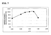
- the phosphor according to the first aspect is provided, which is given as the composition formula expressed by 0.0 ⁇ a/m ⁇ 2.0, 4.0 ⁇ b/m ⁇ 8. 0, 6.0 ⁇ (a + b) /m ⁇ 8.0, 0 ⁇ o/m ⁇ 3.0.
- the phosphor according to any one of the first to third aspects is provided, wherein under excitation by a monochromatic light in the wavelength range from 350nm to 430nm, when a maximum emission intensity in the wavelength range from 400nm to 500nm is defined as P max , and a minimum emission intensity is defined as P min in this range, P min /P max is ⁇ 0.3.
- the phosphor according to any of the first to fourth aspects wherein an element M is more than one kind of element selected from the group consisting of Mg, Ca, Sr, Ba, Zn and rare earth elements having bivalent valency, an element A is more than one kind of element selected from the group consisting of A1, Ga, In, Tl, Y, Sc, P, As, Sb, and Bi, the element B is more than one kind of element selected from the group consisting of Si, Ge, Sn, Ti, Hf, Mo, W, Cr, Pb, Zr, and the element Z is more than one kind of element selected from the group consisting of rare earth elements and transitional metal elements.
- an element M is more than one kind of element selected from the group consisting of Mg, Ca, Sr, Ba, Zn and rare earth elements having bivalent valency
- an element A is more than one kind of element selected from the group consisting of A1, Ga, In, Tl, Y, Sc, P, As, Sb, and Bi
- the element B is more
- the phosphor according to any one of the first to fifth aspects wherein the element M is more than one kind of element selected from the group consisting of Mg, Ca, Sr, Ba, Zn, the element A is more than one kind of element selected from the group consisting of Al, Ga, In, the element B is Si and/or Ge, and the element Z is more than one kind of element selected from the group consisting of Eu, Ce, Pr, Tb, and Mn.
- the phosphor according to any one of first to sixth aspects is provided, wherein the element M is Sr, the element A is Al, the element B is Si, and the element Z is Eu.
- the phosphor according to any one of the first to seventh aspects is provided, wherein when the general formula is expressed by MmAaBbOoNn:Zz, the value of z/(m + z), which is a molar ratio of the element M to the element Z, is 0.0001 or more and 0.5 or less.
- the phosphor according to any one of the first to eighth aspects is provided, containing Sr of 16.0 to 25.0 wt%, Al of 2.0 to 9.0wt%, O of 0.5 to 11.5 wt%, N of 23.0 to 32.0 wt%, and Eu of 0 to 3.5 wt%, wherein when the phosphor is irradiated with the light in the wavelength range from 250nm to 430nm, the maximum peak wavelength in the emission spectrum is in a range from 400nm to 500nm.
- the phosphor according to any one of the first to ninth aspects is provided, wherein in an X-ray diffraction pattern by a powder method using CoK ⁇ ray, a diffraction peak with highest intensity is shown in a Bragg angle (2 ⁇ ) range from 35° to 37°, and further in the Bragg angle (2 ⁇ ) range from 23.6° to 25.6°, 33° to 35°, 39.7° to 40.7°, and 43° to 44° of an X-ray diffraction pattern by the powder method, two, two, one, and one characteristic diffraction peaks are shown, respectively and when a relative intensity of the diffraction peak with highest intensity observed in the Bragg angle (2 ⁇ ) range from 35° to 37° is defined as 100%, the relative intensity of the diffraction peaks is not less than 2.0 %, and not more than 40 %.
- the phosphor according to any one of the first to tenth aspects is provided, wherein a crystal of a product phase contained in this phosphor has a structure of an orthorhombic system.
- the phosphor according to any one of the first to eleventh aspects is provided, wherein a unit volume of a crystal lattice of the product phase contained in this phosphor is not less than 345 ⁇ 3 and not more than 385 ⁇ 3 .
- the phosphor according to any one of the first to eleventh aspects is provided, wherein the unit volume of the crystal lattice of the product phase contained in this phosphor is not less than 353 ⁇ 3 and not more than 385 ⁇ 3 .
- the phosphor according to any one of the first to thirteenth aspects is provided, wherein lattice constants of the crystal lattice of the product phase contained in this phosphor are defined as that a is in a range from 7.85 ⁇ to 8.28 ⁇ , b is in a range from 9.26 ⁇ to 9.58 ⁇ , and c is in a range from 4.80 ⁇ to 4.92 ⁇ .
- the phosphor according to any one of the first to fourteenth aspects is provided, wherein a crystallite size (Dx) of the product phase contained in this phosphor particle is 50nm or more.
- the phosphor according to any one of the first to fourteenth aspects is provided, wherein the crystallite size (Dx) of the product phase contained in this phosphor particle is 80nm or more.
- the phosphor according to any one of the first to sixteenth aspects is provided, containing a primary particle with particle size of 50 ⁇ m or less and aggregates in which the primary particle agglutinates, wherein an average particle size (D50) of the powdery phosphor containing the primary particle and the aggregates is 1.0 ⁇ m or more and 50.0 ⁇ m or less.
- D50 average particle size
- a method of manufacturing the phosphor according to any one of the first to seventeenth aspects including the steps of obtaining a mixture by weighing and mixing powdery raw materials of this phosphor; obtaining a fired product by firing the mixture in a firing furnace; and obtaining the phosphor by pulverizing the fired product, wherein in the step of obtaining the fired product by firing the mixture, any one of nitrogen, inert gas such as rare gas, ammonia, mixed gas of ammonia and nitrogen, or mixed gas of nitrogen and hydrogen is used as atmosphere gas during firing.
- nitrogen, inert gas such as rare gas, ammonia, mixed gas of ammonia and nitrogen, or mixed gas of nitrogen and hydrogen is used as atmosphere gas during firing.
- the method of manufacturing the phosphor according to the eighteenth aspect wherein gas containing 80% or more of nitrogen gas is used as the atmosphere gas in the firing furnace.
- the method of manufacturing the phosphor according to the eighteenth aspect or the nineteenth aspect wherein in the step of obtaining the fired product by firing the mixture in the firing furnace, firing of the mixture is performed twice, and between firings, pulverizing and mixing of a fired mixture is performed.
- the method of manufacturing the phosphor according to any one of the eighteenth to twentieth aspects is provided, wherein in the step of obtaining the fired product by firing the mixture in the firing furnace, the firing is performed while circulating the atmosphere gas in the firing furnace set at 0.1ml/min or more.
- the method of manufacturing the phosphor according to the twenty-first aspect wherein first, firing is performed while circulating the atmosphere gas in the firing furnace set at 0.1ml/min or more, and next, firing is performed without circulating the atmosphere gas in the firing furnace.
- the method of manufacturing the phosphor according to any one of the eighteenth to twenty-second aspects wherein in the step of obtaining the fired product by firing the mixture in the firing furnace, the atmosphere gas in the firing furnace is set in a pressurization state of 0. 001MPa or more and 1.0MPa or less.
- the method of manufacturing the phosphor according to any one of the eighteenth to twenty-third aspects is provided, wherein a crucible composed of nitride is used as a firing crucible.
- a phosphor sheet is provided, wherein the phosphor according to any one of the first to seventeenth aspects is dispersed in a resin or glass.
- an emission device having the phosphor of any one of the first to seventeenth aspects or the phosphor sheet of the twenty-fifth aspect, and an emission part emitting light with a first wavelength, for emitting light with the wavelength different from the first wavelength from the phosphor, with a part or all of the light with the first wavelength as an excitation light.
- the emission device according to the twenty-sixth aspect is provided, wherein the first wavelength is the wavelength from 250nm to 430nm.
- the emission device according to the twenty-sixth or twenty-seventh aspect is provided, wherein the correlated color temperature of the emission device is in a range from 10000K to 2000K.
- the emission device according to the twenty-sixth or twenty-seventh aspect is provided, wherein a correlated color temperature of the emission device is in a range from 7000K to 2500K.
- the emission device according to any one of the twenty-sixth to twenty-ninth aspect is provided, wherein an average color rendering index Ra of the emission device is 80 or more.
- the emission device according to any one of the twenty-sixth to thirtieth aspect is provided, wherein a special color rendering index R15 of the emission device is 80 or more.
- the emission device according to any one of the twenty-sixth to thirty-first aspect is provided, wherein the special color rendering index R9 of the emission device is 60 or more.
- the emission device according to any one of the twenty-sixth to thirty-second aspect is provided, wherein the emission part emitting light with the first wavelength is a light emission device (LED).
- LED light emission device
- the phosphor has a high efficient excitation band in the rage of near ultraviolet/ultraviolet, and when the phosphor is excited by the light in the range of the near ultraviolet/ultraviolet, the phosphor has the emission spectrum in the range of blue color (with a peak wavelength in the range from 400nm to 500nm). Therefore, the phosphor having excellent emission efficiency, emission intensity, and luminance can be provided.
- the obtained phosphor is in a powdery state. Therefore, pulverizing is easy and the phosphor can be applied to various places as a paste.
- the average particle size (D50) of this phosphor is not less than 1.0 ⁇ m and not more than 50.0 ⁇ m, and therefore an application density can be increased and an application film with high emission intensity and luminance can be obtained.
- the phosphor of any one of the eighteenth to twenty-fourth aspect can be easily manufactured at a low manufacturing cost.
- various emission devices can be easily manufactured by combining the phosphor sheet and various emission parts.
- the emission device of any one of the twenty-sixth to thirty-third aspects the emission device with high emission intensity, luminance, and high efficiency, having desired emission color can be obtained.
- a phosphor according to this embodiment has a matrix composition given as a general formula expressed by MmAaBbOoNn:Z.
- element M is more than one kind of element selected from the elements having bivalent valency in the phosphor.
- the element A is more than one kind of element having tervalent valency
- element B is more than one kind of element having tetravalent valency
- O is oxygen
- N is nitrogen
- element Z is the element acting as the activator in the phosphor and is more than one kind of elements selected from rare earth elements or transition metal elements.
- the phosphor of this embodiment having the aforementioned characteristics has a high efficient excitation band in the range of the near ultraviolet/ultraviolet, and has an emission spectrum with a broad peak under an excitation of a part or the whole part of light having a wavelength range from 250 nm to 430 nm, with a maximum peak wavelength in the range from 400 nm to 500 nm, whereby a high efficient light emission can be obtained. Therefore, by mixing the phosphor and the phosphor of other suitable color, and by combining with the light emitting part such as the near ultraviolet/ultraviolet LED, the high efficient light emission device having a desired emission color and high emission intensity and luminance can be obtained.
- the phosphor of this embodiment has not only the excellent emission intensity and luminance compared to a phosphor La 1-x Si 3 N 5 :Ce x containing nitrogen as has been reported heretofore (for example, see patent document 1), but also exhibits excellent emission characteristics, when compared to BAM : Eu, Sr 5 (PO 4 ) 3 Cl:Eu, ZnS:Ag, (Sr, Ca, Ba, Mg) 10 (PO 4 ) 6 Cl 2 :Eu, which are used as a white LED illuminating blue phosphor at present, to thereby make it possible to manufacture the white LED illumination having further high luminance.
- An oxide phosphor BAM:Eu and a halophosphate phosphor SCAP:Eu used at present have excitation bands which rapidly fall, on the longer wavelength side of the wavelength of 380 nm or more, which is the near ultraviolet/ultraviolet region.
- the phosphor of this example contains nitrogen and therefore has a large ratio of covalent bonding compared to the oxide phosphor, and has an excellent excitation band up to the longer wavelength side, compared to the oxide phosphor and the halophosphate phosphor used at present. Therefore, when the white LED illumination is manufactured by combining with the near ultraviolet/ultraviolet LED, the variance in the color tone of the white light can be suppressed.
- the phosphor of this embodiment has the high efficient excitation band in the range of the near ultraviolet/ultraviolet, and has the emission spectrum with a broad peak, with the maximum peak wavelength in the range from 400 nm to 500 nm, under the excitation of the light in the wavelength range from 250 nm to 430 nm, whereby the high efficient light emission can be obtained.
- the activator serving as the center of light emission can regularly exist in a distance not allowing concentration quenching to occur in a crystal structure of the phosphor, and an excitation energy used for light emission, which is given by the excitation light, is efficiently transferred. This contributes to improving the emission efficiency.
- the phosphor when the phosphor is thus constituted, chemically stable composition is thereby realized. Therefore, an impurity phase not contributing to light emission is hardly generated, and it appears that deterioration in emission intensity is suppressed. In other words, when a plurality of impurity phases are generated, the phosphor per unit area is decreased, and further the emission efficiency is deteriorated and the high emission intensity is not obtained, when the impurity phases thus generated absorb the excitation light and the light generated from the phosphor.
- the element M is the element having bivalent valency
- the element A is the element having tervalent valency
- element B is the element having tetravalent valency
- the element M takes an ideal structure surrounded by the tetrahedral [SiN 4 ] or [(Al, Si)(O,N) 4 ]. This contributes to improving the emission efficiency as the phosphor and is preferable.
- x is in a range satisfying 0 ⁇ x ⁇ 2, and more preferably satisfying 0 ⁇ x ⁇ 1.0.
- P min /P max is preferably 30% or more. This is because when 30% or more of P min /P max is maintained, it is possible to obtain the phosphor capable of emitting efficiently stably emitting the light with the prescribed wavelength, even if various excitation sources emitting light of ultraviolet or near ultraviolet with the wavelength range from 350nm to 430nm or the emission wavelength of the emission element is varied or fluctuated.
- the element M is more than one kind of element selected from a group consisting of Mg, Ca, Sr, Ba, Zn, and rare earth elements having bivalent valency, more preferably is more than one kind of element selected from the group consisting of Mg, Ca, Sr, Ba, and Zn, and most preferably is Sr or Ba. In any case, preferably the element M contains Sr.
- the element A is more than one kind of element selected from a group consisting of Al, Ga, In, Tl, Y, Sc, P, As, Sb, and Bi, more preferably is more than one kind of element selected from the group consisting of Al, Ga, and In, and most preferably is Al.
- Al AlN, which is nitride, is used as a general thermoelectric material and structural material, and is easily available at a low cost with a small environmental load.
- the element B is more than one kind of element selected from the group consisting of Si, Ge, Sn, Ti, Hf, Mo, W, Cr, Pb, Zr, more preferably is Si and/or Ge, and most preferably is Si.
- Si Si 3 N 4 , which is nitride, is used as a general thermoelectric material and structural material, and is easily available at a low cost with a small environmental load.
- the element Z is more than one kind of element selected from the group consisting of the rare earth elements or transition metal elements, which is blended in the form of replacing a part of the element M in a matrix structure of the phosphor. From the viewpoint of exhibiting a sufficient color rendering properties by various light sources such as a white LED illumination using the phosphor of this embodiment, it is preferable that the half value width of the peak in the emission spectrum of this phosphor is broad. From this viewpoint, preferably the element Z is more than one kind of element selected from the group consisting of Eu, Ce, Pr, Tb, Yb, and Mn. Among these elements, when Eu is used as the element Z, the phosphor exhibits a blue and broad emission spectrum with high emission intensity. Therefore, Eu is preferable as the activator of each kind of light source such as the white LED illumination.
- the value of the z /(m + z) is in the range of not less than 0.001 and not more than 0.30.
- an optimal value of the range of the value of the z/ (m + z) is slightly fluctuated according to the kind of the activator (element Z) and the kind of the element M.
- the peak wavelength of the emission of the phosphor can be set to be shifted, and this is effective when adjusting the luminance and chromaticity in the light source to be obtained.
- the peak wavelength of the light emission in the phosphor of this embodiment can be varied, and by activating with a different plurality of elements Z, the peak wavelength can be varied and further the emission intensity and luminance can be improved by a photosensitizing effect.
- the phosphor contains Sr of 16.0wt% to 25.0wt%, Al of 2.0wt% to 9.0wt%, O of 0.5wt% to 11.5wt%, N of 23.0wt% to 32.0wt%, and Eu of 0 to 3.5wt%.
- an analysis error of ⁇ 2.0wt% is estimated in Sr and Al, and remaining weight is Si and other elements.
- the concentration of each element of Fe, Ni, and Co in the phosphor is preferably 100ppm or less, and the concentration of B (boron) and C (carbon) is 0.1wt% or less.
- FIG.2 shows the powder X-ray diffraction pattern by CoK ⁇ ray of the phosphor according to examples 2, 4, 6, and a comparative example 2 as will be described as an example of the phosphor according to the present invention, wherein the Bragg angle (2 ⁇ ) of a main peak and the intensity are compared.
- the diffraction pattern shown in the lowermost part is the diffraction pattern of Sr 2 Al 2 Si 10 O 9 N 14 described in the JCPDS card (53-0636), and a non-patent document J.Mater.Chem.,1999,9 1019-1022 .
- an overall patter of a main diffraction peak of the phosphor thus obtained has a resemblance to the pattern of the diffraction peak of Sr 2 Al 2 Si 10 O 4 N 14 which is reported in JCPDS card.
- the peak of the phosphor of the present invention shifts in a direction of enlarging the Bragg angle (2 ⁇ ), compared to a main peak of Sr2Al 2 Si 10 O 4 N 14 crystal reported in the JCPDS card. Therefore, although there is a resemblance between both patterns, it appears that they have different crystal structures with different crystal face interval.
- the difference in oxygen amount present in both crystal structures, and the fact that a part of Sr is replaced with Eu in the phosphor of the present invention, can be considered as factors of giving aforementioned difference between crystal structures of both patterns.
- the overall pattern of the main peak is similar to each other, it appears that the crystal of the product phase of the phosphor of the present invention has a crystal system of a hexagonal crystal system shown by space group Imm2 in the same way as the Sr 2 Al 2 Si 10 O 4 N 14 crystal reported in the JCPDS card.
- the phosphor of the present invention is similar to the Sr 2 Al 2 Si 10 O 4 N 14 crystal reported in the JCPDS card, it has a new crystal structure with different crystal face interval. Therefore, the structure of the phosphor of the present invention having such a new crystal structure is defined by the X-ray diffraction pattern shown by the phosphor, a length (lattice constant) of a crystal axis and a unit volume of the crystal lattice.
- a diffraction peak with highest intensity is shown in a Bragg angle (2 ⁇ ) range from 35° to 37°, and further in the Bragg angle (2 ⁇ ) range from 23.6° to 25.6°, 33° to 35°, 39.7° to 40.7°, and 43° to 44° of an X-ray diffraction pattern by the powder method, two, two, one, and one characteristic diffraction peaks are shown, respectively and when a relative intensity of the diffraction peak with highest intensity observed in the Bragg angle (2 ⁇ ) range from 35° to 37° is defined as 100%, the relative intensity of the diffraction peaks is not less than 2.0 %, and not more than 40 %.
- the diffraction peak with 10 % or more relative intensity in the Bragg angle (2 ⁇ ) range from 26° to 33°, 38.7° to 39.7°, and 42.0° to 42.8°, when the relative intensity of the diffraction peak with highest intensity which is observed in the Bragg angle (2 ⁇ ) range from 35° to 37° is defined as 100 %.
- the diffraction peak observed in the aforementioned range is caused by an impurity phase different from the phase having the emission spectrum with a peak in the wavelength range from 400 nm to 500 nm.
- this impurity phase when this impurity phase is insufficient, it is possible to prevent the deterioration of the emission efficiency caused by absorbing the excitation light or the light emitted from the phosphor by the generated impurity phase, thus making it possible to obtain high emission intensity.
- the diffraction peak with highest intensity in the Bragg angle (2 ⁇ ) range from 35° to 37° is focused. Then, it is found that by containing Al in constituent elements, there are two peaks (see X-ray diffraction pattern of examples 2, 4, 6 and examples 13, 20, 45, 49, 52 in FIG.2 and FIG.8 as will be described later). Then, it was found that the phosphor having the X-ray diffraction pattern with two peaks (in the aforementioned range) by adding Al, is liable to have a more excellent emission characteristic.
- the inventors of the present invention performed crystal structure analysis of a phosphor sample by using a Rietveld method based on the powder X-ray measurement result.
- the Rietveld method is a method of comparing a measurement diffraction intensity of the X-ray obtained from an actual measurement and a diffraction intensity of the X-ray obtained by calculation logically from a crystal structure model assembled by estimating this crystal structure, and making various structure parameters in the latter model more precise by a minimum square method to make the difference between the above-described both diffraction intensities, thereby introducing a model of more precise crystal structure.
- a program "RIETAN-2000" is used for the Rietveld analysis, and the crystal structure of Sr 2 Al 2 Si 10 O 4 N 14 reported in the JCPDS card 53-0636 is used as a reference crystal structure.
- the inventors of the present invention reaches a viewpoint that since the crystal lattice and the volume of the crystal structure are related to Al and an amount of oxygen contained in the crystal structure, the emission characteristic such as emission efficiency of the phosphor is influenced by the Al and the amount of oxygen. Also, since the Al and the amount of oxygen defines the volume of the crystal lattice, the inventors of the present invention reaches the viewpoint that there is the volume of the crystal lattice capable of obtaining the phosphor having the excellent emission efficiency, and founds that the volume of this crystal phosphor is 345 ⁇ 3 to 385 ⁇ 3 , further preferably the volume is 353 ⁇ 3 to 385 ⁇ 3 .
- the inventors of the present invention reach the point that there is the lattice constant of the crystal lattice capable of obtaining the phosphor having excellent emission efficiency, and founds that this lattice constant is defined so that "a” is 7.85 ⁇ to 8.28 ⁇ , "b” is 9.26 ⁇ to 9.58, and "c” is 4.80 ⁇ to 4.92 ⁇ .
- the a-axis, b-axis, and c-axis are taken with reference to the JCPDS card. Accordingly, depending on how to take the axes, the order of the a-axis, b-axis, and c-axis may be replaced, without changing the meaning.
- crystallite size As the crystallite size becomes larger, crystallinity of the manufactured phosphor particle is excellent, and the improvement of the emission efficiency is expected. From this point of view, it is found by the inventors of the present invention that when the crystallite size is 20nm or more, preferably 50nm or more, and further preferably 80nm or more, sufficient emission intensity can be obtained when this phosphor is used as the emission device.
- the average particle size of this phosphor is set at 50 ⁇ m or less. This is because it appears that emission mainly occurs on the surface of the particle in the phosphor powder, and therefore by setting the average particle size (note that in the present invention, the average particle size refers to a median diameter (D50).) at 50 ⁇ m or less, the surface area per unit weight of the powder can be secured, thus making it possible to prevent the deterioration of the luminance. Further, when the powder is formed into a paste and applied to a light emitting element, etc, density of this powder can be improved, and from this viewpoint also, the deterioration of the luminance can be prevented.
- D50 median diameter
- the average particle size is preferably set at 1.0 ⁇ m or more, from the viewpoint of the emission efficiency of the phosphor powder.
- the average particle size of the phosphor powder according to the present invention is preferably set at 1.0 ⁇ m to 50 ⁇ m, and further preferably set at 5.0 ⁇ m to 30 ⁇ m.
- the average particle size (D50) here is the value measured by LS230 (a laser diffraction and scattering method) by Beckman Coulter, Inc.
- the specific surface area (BET) of the phosphor powder of the present invention is preferably set at 0.05m 2 /g to 5.00m 2 /g.
- the phosphor of this embodiment has the emission spectrum with a peak in the range from 400 nm to 500 nm with a broad peak shape, has an excellent emission intensity and luminance, and therefore is suitable for the white LED illuminating phosphor. Further, the phosphor of this embodiment has the emission spectrum with an excellent excitation band in the range of the near ultraviolet/ultraviolet, and therefore, it can be used in a condition which is closer to a maximum emission intensity, when used in the white LED illumination system in which white color is obtained by using a mixed state of the light obtained from the R, G, B and other phosphor, by combining the LED emitting the near ultraviolet/ultraviolet light (near the wavelength range from 380 to 410 nm) proposed as the one-chip type white LED illumination and the red (R) color emitting phosphor, the green (G) color emitting phosphor, and the blue (B) color emitting phosphor excited by the near ultraviolet/ultraviolet light generated from the LED. Specifically, by combining
- a phosphor mixture containing the phosphor of this embodiment is prepared, and by combining with the light emitting part for emitting light with the wavelength range from 250 nm to 450 nm, preferably the wavelength range from 350 nm to 430 nm, various kinds of illumination devices and mainly a backlight for a display apparatus can be manufactured.
- red phosphor to be combined with Y 2 O 2 S:Eu, La 2 O 2 S:Eu, 3.5MgO.0.5MgF 2 .GeO 2 :Mn, (La, Mn, Sm) 2 O 2 S.Ga 2 O 3 :Eu, SrS:Eu, CaS:Eu, Sr 2 Si 5 N 8 :Eu, (Ca, Sr) 2 Si 5 N 8 :Eu, (Ba, Sr, Ca) 3 MgSi 2 O 8 :Eu, Mn, CaAlSiN 3 :Eu are given as examples, however this is not limited thereto.
- the LED light emitting element for emitting light in the wavelength range from ultraviolet to near ultraviolet and a discharge lamp generating ultraviolet light can be used.
- the phosphor mixture containing the phosphor of this embodiment is combined with the discharge lamp generating ultraviolet light, the LED light emitting element, the fluorescent lamps, the illumination unit, and the display device can be manufactured.
- the illumination unit and the display device can be manufactured.
- the display device can be manufactured.
- a method of combining the phosphor mixture of this embodiment and the light emitting part may be performed by the publicly-known method.
- the light emission device can be manufactured as will be described below. The light emission device using the LED in the light emitting part will be explained hereunder, with reference to the drawings.
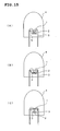
- FIG. 15 (A) to FIG. 15 (C) are schematic sectional views of general type LED light emission devices
- FIG.16(A)to FIG. 16 (E) are schematic sectional views of reflective type LED light emission devices. Note that the same signs and numerals are assigned to the corresponding part in each drawing, and explanation is omitted in some cases.
- an LED light emitting element 2 is set in a cup case 5 provided on the point of a lead frame 3, and is molded by a translucent resin 4.
- the cup case 5 is totally buried with the phosphor mixture and a mixture obtained by dispersing the phosphor mixture in a translucent resin such as silicon and epoxy.
- a dispersed material of light such as SiO 2 and Al 2 O 3 may be preferably contained in the resin.
- FIG.15(B) explanation will be given to an example of a different light emission device.
- a mixture 1 is applied on the cup case 5 and the upper surface of the LED light emitting element 2.
- FIG.15(C) explanation will be given to an example of a further different light emission device.
- the phosphor mixture 1 is set on the upper part of the LED light emitting element 2.
- the light emission device can be prepared by the same method.
- the reflective type LED light emission device is provided, in which a reflecting surface and a reflecting board are formed in a light releasing direction of the LED light emitting element 2, and the light released from the light emitting element 2 is reflected by the reflecting surface and emitted outside. Therefore, by using FIG.16(A) to FIG.16(E), explanation will be given to the light emission device in which the reflective type LED light emission device and the phosphor mixture of this embodiment are combined.
- the reflective type LED light emission device in which the reflective type LED light emission device is used in the light emitting part, with the reflective type LED light emission device and the phosphor mixture of this embodiment combined.
- the LED light emitting element 2 is set on the tip end of one lead frame 3, and the light is emitted from the LED light emitting element 2, directing downward, then reflected by a reflecting surface 8, which is then released from the upper part.
- the mixture 1 is applied on the reflecting surface 8. Note that a recessed portion formed by the reflecting surface 8 is sometimes filled with a transparent mold material 9 for protecting the LED light emitting element 2.
- FIG.16(B) explanation will be given to an example of a different light emission device.
- the mixture 1 is set at a lower part of the LED light emitting element 2.
- FIG.16(c) explanation will be given to an example of the different light emission device.
- the recessed portion formed by the reflecting surface 8 is filled with the mixture 1.
- FIG.16(D) explanation will be given to an example of the different light emission device.
- the mixture 1 is applied on the upper part of the transparent mold material 9 for protecting the LED light emitting element 2.
- FIG.16(E) explanation will be given to an example of the different light emission device.
- the mixture 1 is applied on the surface of the LED light emitting element 2.
- the general type LED light emission device and the reflective type LED light emission device may be used selectively depending on the application.
- the reflective type LED light emission device has an advantage that it can be made thin, a light emitting area can be made large, and use efficiency of the light can be improved.
- the light emission device thus explained is used as an illuminating light source with high color rendering properties, it is necessary to have the emission spectrum with excellent color rendering properties. Therefore, by using an evaluation method of JIS Z 8726, the color rendering properties of the light emission device incorporating the phosphor mixture containing the phosphor of this embodiment was evaluated.
- the evaluation of the JIS Z 8726 when a general color rendering index value Ra of the light source is set at 80 or more, the light source is regarded as an excellent light emission device.
- a special color rendering index value R15 which is an index showing a skin color component of a Japanese woman, is set at 80 or more, the light source is regarded as the excellent light emission device.
- the aforementioned index may not be satisfied, depending on the application not requiring the color rendering properties and a different purpose. Therefore, the light emission device was manufactured, by which the phosphor mixture containing the phosphor of this embodiment was irradiated with the light from the light emitting part which emits light with the wavelength range from 250 nm to 430 nm, to cause the phosphor mixture to emit light. Note that an ultraviolet LED for emitting light of 405 nm wavelength was used as the light emitting part.
- the color rendering properties of the light source incorporating the phosphor mixture containing the phosphor of this embodiment exhibited improved values such as Ra set at 80 or more, further preferably R15 set at 80 or more, and R9 set at 60 or more in the range of correlated color temperature from 10000K to 2000K (further preferably 7000K to 2500K), and it was found that the light emission device thus explained was regarded as an excellent light source with high luminance and significantly improved color rendering properties.
- a phosphor sheet may be formed by dispersing the phosphor mixture of the present invention in the resin.
- a material being a medium, used for manufacturing the phosphor sheet, each kind of resin such as epoxy resin and silicon resin, or glass, etc, can be taken into consideration.
- the phosphor sheet and a light source performing suitable emission are combined, and a specific emission can be performed.
- the excitation light whereby the phosphor sheet is excited may be the light in the wavelength range from 250nm to 430nm, and an ultraviolet ray light source by Hg discharge and a light source by laser may be used.
- the mixing amount is preferably adjusted by each firing condition. Therefore, as a matter of convenience, the composition formula calculated by the blending ratio of the phosphor raw materials is shown in the explanation hereunder. Accordingly, in this embodiment, the manufacturing method will be explained, with the phosphor expressed by the composition formula SrAlSi 6.5 O 1.25 N 9.50 :Eu, during mixing of the raw materials.
- z/ (m + z) and Eu/(Sr + Eu) have the same meaning. Note that only slight amount of oxygen is contained in the raw materials of an activator element during mixing, and therefore such an oxygen amount is ignored.
- a plurality of phosphors are manufactured by a solid phase reaction, and the manufacturing method of the phosphor of this embodiment can also be obtained by the solid phase reaction.
- the manufacturing method is not limited thereto.
- Each raw material of the element M, the element A, and the element B may be a commercially available material such as nitride, oxide, carbonate, hydroxide, basic carbonate. However, higher purity is preferable and the raw material with 2N or more, more preferably with 3N or more is therefore prepared.
- the particle size of each particle of the raw materials is generally a fine particle from the viewpoint of accelerating reaction. However, the particle size and the shape of the phosphor obtained are changed according to the particle size and the shape of the raw material.
- the nitride raw material having the particle size approximating to that of the phosphor thus finally obtained may be prepared.
- the raw material having a particle size of 50 ⁇ m or less is preferably used, and the raw material having a particle size of 0.1 ⁇ m to 10.0 ⁇ m is further preferably used.
- the raw material of the element Z also, the commercially available raw material such as nitride, oxide, carbonate, hydroxide, basic carbonate, or simple substance metal is preferable. Of course, higher purity is preferable, and therefore the raw material preferably with the purity of 2N or more, more preferably with the purity of 3N or more is prepared.
- the carbonate is used as the raw material of the element M, an effect of flux can be preferably obtained, without adding the compound composed of the element not contained in the constituent element of the phosphor of this embodiment as the flux (reaction promotor).
- SrCO 3 (3N), Al 2 O 3 (3N), AlN(3N), Si 3 N 4 (3N) may be prepared as the raw materials of the element M, the element A, and the element B, and Eu 2 O 3 (3N) may be prepared as the element Z.
- the raw materials thus prepared are weighed and mixed so as to obtain the mixing ratio of each raw material set at 0.970 mol of SrCO 3 , 0.25/3 mol of Al 2 O 3 , (1.0 - 0.25/3 x 2) mol of AlN, 6.5/3 mol of Si 3 N 4 , and 0.030/2 mol of Eu 2 O 3 respectively.
- the carbonate is used as the Sr raw material.
- an oxide raw material has a high melting point, and therefore the effect of the flux can not be expected, meanwhile, when the raw material having a low melting point such as carbonate is used, the raw material itself acts as the flux, thereby promoting the reaction and improving the emission characteristic.
- a slight amount of C (carbon) may be added to the raw material to improve reducibility during firing.
- the concentration of C contained in the sample after firing needs to be adjusted so as to be 0.1wt% or less.
- another substance may be added as the flux, to obtain the effect of the flux.
- the flux becomes the impurity, thereby posing the possibility of deteriorating the characteristic of the phosphor.
- the weighing and mixing may be performed in an atmospheric air, however the nitride of each raw material element is easily influenced by humidity, and therefore the inert gas from which the humidity is sufficiently removed is preferably used, to operate in a glove box.
- a mixing system may be either way of a wet type or a dry type. However, when pure water is used as the solvent of the wet type mixing, the raw material is decomposed, and therefore proper organic solvent or liquid nitrogen needs to be selected.
- a usual device such as a ball mill or a mortar may be used. Note that this flux effect will be explained in an example.
- the raw materials thus mixed are put in a crucible, retained and fired at 1600°C or more, more preferably at 1700°C to 2000°C, for 30 minutes or more, while flowing atmosphere gas into the firing furnace.
- the firing temperature is set at 1600°C or more, the solid reaction progresses preferably and the phosphor having the excellent emission characteristic can be obtained.
- the raw materials are fired at 2000°C or less, excessive sintering and melting can be prevented from occurring.
- the higher the firing temperature is the more rapidly the firing is advanced, and the retaining time can therefore be shortened.
- the target emission characteristics can be obtained by maintaining the temperature for a long time.
- the longer the firing time is, the more rapidly particle growth is advanced, and the particle size becomes large. Therefore, the firing time may be set in accordance with the target particle size.
- An atmosphere gas flown into the firing furnace is not limited to nitrogen, and any one of the gases of inert gas such as rare gas, ammonia, mixed gas of the ammonia and nitrogen, or mixed gas of the nitrogen and hydrogen may be used.
- the oxygen is contained in the atmosphere gas, oxidizing reaction of the phosphor particle occurs. Therefore, the oxygen contained as the impurity is reduced as much as possible, and is preferably reduced to 100ppm or less.
- the humidity contained as the impurity is reduced as much as possible, and is preferably reduced to 100ppm or less, for example.
- the ammonia when a single gas is used as the atmosphere gas, nitrogen gas is preferable. Although firing by independent use of the ammonia gas is possible, the ammonia gas is more expensive than the nitrogen gas in terms of cost and is corrosive gas. Therefore, a special treatment is needed in a device and an exhaustion method at a low temperature. Accordingly, when the ammonia is used, preferably the ammonia is set in a low concentration such as being mixed with nitrogen. For example, when the mixed gas of the nitrogen gas and the ammonia is used, 80% or more of the nitrogen and 20% or less of the ammonia are preferably used.
- an inactive or a reductive gas containing 80% or more of nitrogen may be preferably used.
- firing is performed with the aforementioned gas atmosphere being kept flowing in the furnace at a flow rate of 0.1 ml/min or more.
- gas is generated from the raw material during firing, by flowing the atmosphere containing one or more kind of gas selected from the aforementioned inert gas such as nitrogen and rare gas, ammonia, mixed gas of the ammonia and the nitrogen, or the mixed gas of the nitrogen and hydrogen, the furnace can be prevented from being filled with the gas generated from the raw materials, resulting in having an influence on the reaction, and consequently the deterioration in the emission characteristic of the phosphor can be prevented.
- the raw material which is decomposed into oxides at high temperature such as carbonate, hydroxide, and basic carbonate is used, a large amount of gas is generated. Therefore, preferably by flowing the gas in a firing furnace, generated gas is exhausted.
- the pressure in the firing furnace is preferably set in a pressurized state so as not allow the oxygen in the atmospheric air to be mixed into the furnace.
- this pressure exceeds 1.0MPa (in the present invention, an in-furnace pressure means a pressurized amount from the atmospheric air.)
- the pressurized amount is preferably 1.0MPa or less in consideration of productivity.
- the in-furnace pressure during firing is preferably set at 1.0MPa or less, and further preferably set at 0.001MPa to 0.1MPa.
- the crucible may be used, such as an Al 2 O 3 crucible, a Si 3 N 4 crucible, an A1N crucible, a sialon crucible, a C (carbon) crucible, and a BN (boron nitride) crucible, which can be used in the aforementioned gas atmosphere.
- the crucible composed of nitride is preferable, and when the BN crucible is used, intrusion of impurities from the crucible can be averted and this is preferable.
- 0.1wt% or less of B(boron) and/or C is contained as an amount of impurities after firing, the emission characteristic is not inhibited and this is preferable.
- a fired matter is taken out from the crucible. Then, by using a pulverizing means such as the mortar and the ball mill or the like, the fired matter is pulverized to obtain a prescribed average particle size, and the phosphor expressed by the composition formula SrAl 0.8 Si 5.2 O 1.8 N 7.2 :Eu can be manufactured.
- the phosphor thus obtained is subjected to cleaning, classifying, surface treatment, and heat treatment as needed.
- cleaning in an acid solution using fluorinated acid, hydrochloric acid, sulfuric acid, and nitric acid is preferable, because metal atom such as Fe adhered to the surface of the particle and a raw material particle which is unreacted and remained can be resolved.
- amounts of Fe, Ni, and Co contained in the phosphor thus obtained are preferably 100ppm or less.
- the phosphor can be manufactured by the same manufacturing method as that described above, by adjusting the blending amount of each raw material during mixing to a predetermined composition ratio.
- a firing condition evaporation or sublimation of raw materials occurs during firing, and therefore mixing/firing of the raw materials is performed in consideration of the mixing composition of the raw materials by an amount of such evaporation/sublimation.
- example 1 The present invention will be more specifically explained, based on examples.
- the example 1 was manufactured by the following procedure.
- the composition formula thus obtained is calculated from the blending ratio of the raw materials used. Accordingly, the sublimation of Si and the reduction of oxygen occur during firing. Therefore, in a phosphor product after firing, the composition of less amount of Si or oxygen than the blending ratio of the raw materials (mixing composition ratio) can be considered.
- the emission peak wavelength and the emission intensity were measured.
- the measurement result is shown in table 1 and FIG.1.
- the emission peak wavelength refers to the wavelength shown by a maximum peak value of the spectrum of the light released by the phosphor, when the phosphor is irradiated with the light of some wavelength or energy
- the emission intensity refers to an intensity in the peak wavelength of this emission. Note that the emission spectrum and an excitation spectrum as will be described later were measured by using a spectrofluorometer FP-6500 by JASCO Corporation.
- FIG.1 is a graph showing the relative intensity of the emission intensity of the phosphor sample taken on the ordinate axis, and showing the value of the b/m ratio taken on the abscissa axis.
- the X-ray diffraction pattern by a powder method was measured, for the samples of the examples 2, 4, 6, and the comparative example 2. Further, a Rietveld analysis was performed to the sample of the example 4.
- FIG.2 the X-ray diffraction pattern is shown in an order of comparative example 2, examples 2, 4, 6, a Rietveld analysis result and the diffraction pattern of the JCPDS card (53-0636) from upside.
- the sample with the value of the b/m ratio set at 3 or less according to the comparative examples 1 and 2 was an orange phosphor having the emission spectrum with a peak in the vicinity of the wavelength of 630nm, not having the peak of the emission spectrum in the wavelength range from 400nm to 500nm.
- the phosphor to be measured was pulverized up to a predetermined (preferably from 1.0 ⁇ m to 50.0 ⁇ m) average particle size by using pulverizing means such as the mortar and the ball mill after firing. Then, a titanium holder was filled with the phosphor thus pulverized to form a flat surface, and the X-ray diffraction pattern was measured by an XRD apparatus by RIGAKU DENNKI INC., "RINT 2000". The measurement result is shown below.
- the deviation of the Bragg angle (2 ⁇ ) is caused by a not flat sample surface to be irradiated with X-ray, a measurement condition of the X-ray, and particularly by the difference in scan speed or the like. Therefore, a slight deviation is considered to be allowable in the range where a characteristic diffraction peak is observed.
- the scan speed is set at 0.3°/min and then Si is mixed in the phosphor sample, and the deviation of the Si peak is corrected after X-ray measurement, to thereby obtain the Bragg angle (2 ⁇ ) and a surface interval d( ⁇ ).
- the same measurement was performed for the sample of examples 13, 20, 45, 49, 52, and the samples of an example 45 and the comparative example 3 as shown in FIG.13.
- the X-ray diffraction pattern of example 4 showing strong emission intensity and the X-ray diffraction pattern of the comparative example 2 not having the emission peak in the wavelength range from 400nm to 500nm, and the X-ray diffraction pattern of the examples 2 and 6 having smaller emission peak than the emission peak of the example 4 are compared. Then, in the comparative example 2 and the examples 2 and 6, many diffraction peaks can be confirmed in the Bragg angle (2 ⁇ ) in which no diffraction peak is observed in the example 4.
- the diffraction peaks can be confirmed in the Bragg angle (2 ⁇ ) range from 26° to 33°, 38.7° to 42.8°.
- the diffraction pattern of the comparative example 2 although the diffraction pattern similar to the example 4 can be observed, its generation ratio is about 40% of an entire phosphor product phase, and it is found that other many product phases considered to be yellow phosphors are contained. Namely, it appears that the diffraction peak in the Bragg angle (2 ⁇ ) range from 26° to 33°, 38.7° to 42.8° is caused by a different phase (impurity phase) from the phase showing the peak of the emission spectrum in the wavelength range from 400nm to 500nm.
- the phosphor having the peak of the emission spectrum in the wavelength range from 400nm to 500nm and strong emission intensity Preferably, 50% or more of the above-described product phases (the phases similar to SrAl x Si 6-x O 1+x N 8-x ) are contained and the phosphor does not have the diffraction peak shown by these impurity phases.
- Fig.2 shows the diffraction pattern simulated based on the crystal structure of Sr 2 Al 2 Si 10 O 4 N 14 reported in the JCPDS card (53-0636), and a simulation result obtained by subjecting the X-ray diffraction pattern of the example 4 to Rietbeld analysis based on the crystal structure of the Sr 2 Al 2 Si 10 O 4 N 14 .
- the SrSi 6 N 8 crystal structure reported in the non-patent document Z.Anorg.Allg.Chem.,2004,630,1729 has a orthorhombic crystal structure similar to the Sr 2 Al 2 Si 10 O 4 N 14 crystal reported in the JCPDS card.
- the phosphor of the present invention has a similar crystal structure as that of the Sr 2 Al 2 Si 10 O 4 N 14 reported in the JCPDS card and the SrSi 6 N 8 reported in the Z.Anorg.Allg.Chem.,2004,630,1729, this phosphor is a new phosphor having a new crystal structure of different crystal face interval and having the composition formula expressed by SrAl x Si 6-x O 1+x N 8-x , by changing an existence amount of the Al or oxygen atom.
- the volume of the crystal lattice must be between the crystal structure of Sr 2 Al 2 Si 10 O 4 N 14 and the crystal structure of SrSi 6 N 8 , namely, a crystal volume must be 345 ⁇ 3 or more and 385 ⁇ 3 or less.
- x is preferably in a range of 0 ⁇ x ⁇ 2, and is preferably 0 ⁇ x ⁇ 1.0 with smaller lattice constant and unit constant.
- the diffraction pattern is close to the diffraction pattern obtained from the analysis result, and no diffraction peak of the impurity phase exists, which is observed in the Bragg angle range from 26° to 33°, 38.7° to 39.7°, and 42.0° to 42.8°.
- the aforementioned impurity peak is 10.0% or less, when the relative intensity of the diffraction peak with strongest intensity observed in a range of 35° to 37° is set at 100%.
- a replacement amount of Si by Al preferably an amount of Si is also changed to have a suitable structure for emission.
- the amount of Si is changed correspondingly to the replacement amount of the changed Al, to have a suitable structure for emission.
- the mixing composition of Si and the amount of oxygen during weighing/mixing of the raw materials are changed, and the mixing composition and a target composition for obtaining the phosphor having the strong emission intensity were examined.
- the examples 7 to 15 were manufactured in the following procedure.
- the peak wavelength and the emission intensity were measured for the manufactured samples of the examples 7 to 15. This measurement result is shown in table 2 and FIG.3.
- the relative intensity of the emission intensity of the phosphor sample is taken on the ordinate axis, and the o/m ratio is taken on the abscissa axis.
- the light with the wavelength of 405nm was used as the excitation light.
- the examples 16 to 24 were manufactured by the following procedure.
- the peak wavelength and the emission intensity were measured for the manufactured samples of the examples 16 to 24. This measurement result is shown in table 3 and FIG.4.
- the relative intensity of the emission intensity of the phosphor sample is taken on the ordinate axis, and the o/m ratio is taken on the abscissa axis.
- the light with the wavelength of 405nm was used as the excitation light.
- the examples 25 to 30 were manufactured by the following procedure.
- Commercially available SrCO 3 (3N), Al 2 O 3 (3N), A1N(3N), Si 3 N 4 (3N), and Eu 2 O 3 (3N) were prepared as the raw materials, and in the same way as the example 1, the phosphor sample was manufactured excepting that the mixing ratio of each raw material was adjusted so that each raw material had a prescribed a/m ratio.
- the raw material mixing amount and a measurement result of the phosphor sample of the examples 25 to 30 are shown in table 4 and FIG.5.
- FIG.5 shows a graph in which the emission intensity of the phosphor samples of the examples 25 to 30 is plotted, with the relative intensity of the emission intensity of the phosphor samples taken on the ordinate axis, and the a/m ratio taken on the abscissa axis.
- the impurity phase having the emission peak in the vicinity of the wavelength of 600nm is considered to correspond to a Sr-Al-Si-O-N:Eu based phosphor shown in the patent application No.2005-61627.
- the blue phosphor of the present invention and the yellow and orange phosphor generated as the impurity phases are simultaneously generated and mixed. Therefore, by irradiating the phosphor with the excitation light with the wavelength from 250nm to 430nm, the lights of the blue color and yellow color are mixed, thereby obtaining the emission color of white. Therefore, this phosphor can be used as the phosphor for the emission device showing white emission individually.
- the examples 31 to 35 were manufactured by the following procedure.
- Table 5 and FIG.6 show the raw material mixing amount and the measurement result of the phosphor samples of the examples 31 to 35.
- FIG. 6 shows a graph in which the emission intensity of the phosphor samples of the examples 31 to 35 is plotted, with the relative intensity of the emission intensity of the phosphor samples taken on the ordinate axis, and the value of Eu/ (Sr + Eu) taken on the abscissa axis.
- the sample of adding MnO 2 SrF 2 , BaCl 2 , AlF 3 , BaO, SrCl 2 , GaN, and Li 2 CO 3 to the phosphor sample having the composition of the example 20 was manufactured, and the average particle size (D50), the specific surface area (BET), and the emission characteristic (the emission intensity and the peak wavelength) of the obtained phosphor were measured.
- the examples 36 to 44 were manufactured by the following procedure.
- the commercially available SrCO 3 (3N), AlN(3N), Al 2 O 3 , Si 3 N 4 (3N), and Eu 2 O 3 (3N) were prepared as the raw materials, and commercially available SrF 2 , BaCl 2 , AlF 3 , MnO 2 , BaO, SrCl 2 , GaN, LiCO 3 were prepared as additives.
- each raw material was weighed to obtain a mixed raw material. 1.0wt% of each additive was added to the mixed raw material before firing and mixed therein by using the mortar under the atmospheric air.
- MnO 2 was added in the example 37
- SrF 2 was added in the example 38
- BaCl 2 was added in the example 39
- AlF 3 was added in the example 40
- BaO was added in the example 41
- SrCl 2 was added in the example 42
- GaN was added in the example 43
- LiCO 3 was added in the example 44, respectively.
- No additive was added to the example 36, and the example 36 and the example 20 have the same composition.
- the raw materials thus mixed were put in the BN crucible, and after vacuously exhausting the inside of the furnace once, temperature was increased at 15°C/min up to 1800°C with the pressure in the furnace set at 0.05 MPa in the nitrogen atmosphere (flow state at 20.0 L/min), and the raw materials were retained/fired at 1800°C for 3 hours, then, the temperature was decreased from 1800°C to 50°C to cool the raw materials for 90 minutes. Thereafter, a fired sample was pulverized by using the mortar up to a proper particle size in the atmospheric air, to thereby obtain the phosphor sample of the examples 36 to 44.
- the average particle size (D50) and the specific surface area (BET) were measured, for the phosphor sample of the samples 36 to 44, and these phosphor samples were irradiated with the light with the wavelength of 405nm, to measure the peak wavelength and the emission intensity. Then, the emission intensity was measured, with the emission intensity at the peak wavelength of the example 36 standardized as 100%. The measurement result is shown in table 6.
- the example 38 added with SrF 2 being the salt of the constituent element of the phosphor of the present invention and the example 40 added with AlF 3 are the phosphor powder with low BET (or large average particle size D50) while maintaining high emission characteristic, if compared with an additive-free example 36.
- any one of the samples has a smooth particle surface.
- the particle surface is smooth, a dense film can be manufactured when a phosphor film is manufactured by using the aforementioned particle.
- this phosphor film is used as a coating type phosphor film such as a display, the film with high luminance can be obtained.
- the phosphor and the phosphor film with high luminance can be obtained.
- the example 39 added with BaCl 2 and the example 37 added with MnO 2 are compared with the additive-free example 36, it is found that the peak wavelength of the emission spectrum is shifted to the longer wavelength side by about 5.0nm by addition of this additive.
- the peak wavelength of the emission spectrum can be shifted to the longer wavelength side when Ba and Mn are brought into a solid-solution into a phosphor matrix, because the result is obtained such that 2.0wt% of Ba is contained in the example 39 and 1.2wt% of Mn is contained in the example 37.
- the emission spectrum is shifted to the longer wavelength side where naked-eye visibility is high, and therefore for example the luminance of the white LED in which this phosphor is assembled can be improved, and the white LED of various color white LED can be manufactured.
- the emission intensity is substantially not changed when compared with the additive-free example 36, and the phosphor powder with small particle size is obtained.
- chloride, oxide, and nitride are used as the additive, it is found that the phosphor with high luminance due to a peak shift and a fine phosphor film due to a smaller particle size can be obtained in some cases.
- the examples 45 to 50 were manufactured by the following procedure.
- the change of the characteristic was checked, when the o/m ratio (oxygen concentration) of the example 45 was set in the range from 0.5 to 1.5.
- SrCO 3 (3N) and SiO 2 (3N) were prepared as the raw materials for supplying oxygen, other than the commercially available Sr 3 N 2 (2N), Si 3 N 4 (3N), and Eu 2 O 3 (3N), and the sample was manufacture in the same way as the example 45, other than a part of N (nitrogen) of the example 45 was replaced with O (oxygen) by mixing each raw material with a prescribed molar ratio.
- 0.50mol of SrCO 3 , (0.970 - 0.50)/3mol of Sr 3 N 2 , 7/3mol of Si 3 N 4 , and 0.030/2mol of Eu 2 O 3 may be weighed, and in the example 49, 0.970mol of SrCO 3 , (1.25 - 1.00)/2mol of SiO 2 , (7 - (1.25 - 1.00)/2)/3mol of Si 3 N 4 , and 0.030/2mol of Eu 2 O 3 may be weighed.
- the manufactured phosphor samples of the examples 45 to 50 were irradiated with the light with the wavelength of 405nm as the excitation light, and the peak wavelength and the emission intensity were measured. This measurement result is shown in table 7 and FIG.7.
- the o/m ratio becomes larger than 1.25
- the sample is vitrified, and the structure around Eu ion, which is the center of the light emission, is formed irregular, thereby generating variance in distance between luminescence centers, resulting in deterioration in the emission intensity.
- the crystal structure is optimized and the phosphor having the excellent emission characteristic can be obtained.
- the composition analysis result of the phosphor after firing shown in table 7 a tendency that Si and O were reduced from the mixing composition formula was observed.
- the phosphor having a new structure of SrSi 6 N 8 O:Eu with a composition of x 0 not conventionally reported, being the structure of SrSi 6 N 8 :Eu with SrSi 6 N 8 having small amount of Si as the matrix, or the structure of SrAl x Si 6-x O 1+x N 8-x is generated.
- an object is to make the oxygen concentration uniform and realize a uniform dispersion of the Eu element in the phosphor sample, and in a firing step, firing was performed divided into multiple numbers of times.
- the raw materials thus mixed were put in the BN crucible, and after vacuously exhausting the inside of the furnace once, temperature was increased at 15°C/min up to 1600°C with the pressure in the furnace set at 0.05 MPa in the nitrogen atmosphere (flow state at 20.0 L/min), and the raw materials were retained/fired at 1600°C for 3 hours, then, the temperature was decreased from 1600°C to 50°C to cool the raw materials for 90 minutes.
- a fired sample was taken out from the furnace and was pulverized by using the mortar up to a proper particle size in the atmospheric air, and was put in the crucible again and set in the firing furnace. Then, after vacuously exhausting the inside of the furnace once, temperature was increased at 15°C/min up to 1800°C with the pressure in the furnace set at 0.05 MPa in the nitrogen atmosphere (flow state at 20.0 L/min), and the raw materials were retained/fired at 1800°C for 3 hours, then, the temperature was decreased from 1800°C to 50°C to cool the raw materials for 90 minutes, and the fired sample was taken out from the furnace. The obtained sample was pulverized by using the mortar up to a proper particle size in the atmospheric air, to thereby obtain the phosphor of the example 51.
- the firing condition was the same as that of the example 51, firing was performed by air-tightly closing the inside of the furnace without allowing the nitrogen atmosphere to circulate therein, and the sample was manufactured.
- the peak wavelength and the emission intensity of the emission as the emission characteristics were measured for the manufactured samples 51 and 52. This measurement result is shown in table 8. Note that in measuring the emission intensity, the value of the emission intensity in the peak wavelength of the example 20 is standardized as 100%. Note that the monochromatic light with the wavelength of 405nm was used as the excitation light.
- the firing step by performing firing divided into multiple numbers of times, it was found that the emission intensity of the phosphor sample was improved by 10% or more. This is because by mixing/stirring the phosphor sample after first firing and performing second firing or thereafter for the phosphor sample, the composition of the phosphor sample is further made to be uniform and the emission characteristic is improved.
- the oxygen concentration in the phosphor samples is adjusted to the amount of oxygen necessary for maintaining the proper phosphor composition.
- a sample for determining the oxygen concentration in the phosphor sample was manufactured, and an optimal oxygen concentration was obtained by performing the first firing under each condition.
- a sealing method of the firing furnace a method of putting a lid on the crucible filled with the phosphor samples is easy and preferable.
- a sealing effect can be obtained. Therefore, by the method of stopping the circulation of the atmosphere gas for a prescribed time also, the effect of sealing can be similarly obtained.
- Examples 53 to 57 are the same as the phosphor samples of the example 20. However, the phosphor samples were manufactured, with element Ca and element Ba employed as alternatives of element Sr of the phosphor samples.
- the composition of the element M in a phosphor sample composition formula was changed.
- one or more kinds of element M were mixed and used, they were mixed by being adjusted so that the number of moles for the sum total of the element M containing such plurality of elements was constant.
- the blending ratio of the element M of the example 20 was set to be Sr1.0
- the blending ration is adjusted to obtain Sr0.75 : Ba0.25 for the sample of the example 53, Sr0.5 : Ba0.5 for the sample of the example 54, Sr0.25 : Ba0.75 for the sample of the example 55, Ba1.0 for the sample of the example 56, and Ca0.25 : Sr0.75 for the sample of the example 57.
- the manufacturing method of the phosphor sample was performed in the same way as that of the example 20, and the emission intensity and the luminance of the phosphor samples of the examples 53 to 57 were measured.
- the measurement result was explained with reference to the table 9. Note that in measuring the emission intensity and the luminance, the value of the emission intensity and the luminance in the peak wavelength of the emission of the phosphor sample of the example 20 was standardized as 100%. Note that the light with the wavelength of 405nm was used as the excitation light.
- each phosphor of the examples 13, 20, 45, 49, 52 shows the diffraction peak with strongest intensity in the Bragg angle (2 ⁇ ) range from 35° to 37° in the X-ray diffraction pattern by the powder method using the CoK ⁇ ray.
- 2, 2, 1, 1 characteristic diffraction peaks are observed in the Bragg angle range from 23.6° to 25.6°, 33° to 35°, 39.7° to 40.7°, 43° to 44° of the X-ray diffraction pattern, respectively, and when the relative intensity of the diffraction peaks with strongest intensity observed in the Bragg angle range (2 ⁇ ) from 35° to 37° is set at 100%, the relative intensity of these diffraction peaks show 2.0% or more and 40% or less diffraction peaks.
- FIG.9(A) shows a photograph with magnification of 250
- FIG.9(B) shows a photograph with magnification of 1000.
- measurement error or the impurities mixed therein during manufacturing the phosphor can be considered.
- Si 3 N 4 present as the impurity in the sample it can be so considered that the ratio of Sr and Al is seemingly made smaller.
- the generated sample possibly has an oxygen deficit composition, or a composition with less amount of oxygen than the theoretical composition. Accordingly, when the amount of oxygen in the phosphor sample can be properly adjusted by controlling the manufacturing condition, the phosphor with further optimized crystal structure and higher efficiency would be obtained. Note that the analysis result is that the concentration of elements Fe, Ni, Co is 100ppm or less and the concentration of C and B is 200ppm or less in any one of the samples of the examples 13, 20, 42, 52, and an element concentration to deteriorate the emission characteristic is extremely small.
- the average particle size (D50) is measured by a laser Doppler measurement method for the samples of the examples 13, 20, 49, 52, any one of the sample of these examples is sized at not less than 1.0 ⁇ m and not more than 50.0 ⁇ m. Then, when the above samples are formed into a paste and applied on various places, the coating density can be increased, to thereby realize a coating film having high emission intensity and luminance.
- the phosphor powder thus obtained contains a primary particle with particle size of 50.0 ⁇ m or less, and an aggregate in which the primary particles are aggregated each other. Thus, it is found that the aforementioned phosphor powder contains the primary particle and the aggregate thereof. Note that as the primary particle grows, formation of plate-shaped particles is observed. Therefore, from the point of the improvement of crystallinity and the improvement of the emission characteristic, the plate-shaped particles are preferably contained in the first primary particle.
- each phosphor shows the numerical value in the vicinity of 3.42g/cc.
- an Ultrapycnometer 1000 by QUANTACHROME INC., was used.
- the true density shows the numerical value in the vicinity of 3. 60g/cc.
- the true density of this phosphor is a lower value than an ideal value. This is because the generated phosphor sample is more deficient of oxygen than the theoretical composition as shown in the composition analysis result, or has a composition with smaller amount of oxygen than the theoretical composition.
- the true density of the phosphor of the present invention is preferably in the range from 3.40g/cc to 3.65g/cc.
- the emission characteristic is improved with the increase of the crystal lattice volume.
- the crystal lattice volume is preferably 353 ⁇ 3 or more.
- the phosphor powder obtained by the example 52 has a small deficient amount of the oxygen atoms of the 2b site, compared to the phosphor powder obtained by the examples 13, 20, 49, and from the composition analysis result shown in the table 10, the oxygen concentration in the phosphor powder is slightly high. Accordingly, in the phosphor powder obtained by the example 52, it appears that by replenishing the oxygen atoms to an oxygen deficient site in the crystal lattice so as to be further optimized, the crystal lattice volume is increased and the emission characteristic is improved.
- Table 12 and FIG.10 show the result of measuring the temperature characteristic of the emission intensity at temperature from 25°C to 300°C, for the samples of the examples 13, 20, 49, 52.
- emission intensity P 25 at the temperature of 25°C and emission intensity P T at the temperature of T°C, and a measurement of a variation of the emission intensity.
- the aforementioned emission intensity P 25 is obtained by measuring the spectrum of the light emitted by an emitter when the phosphor is placed in an environment of 25°C and is irradiated with the excitation light with a prescribed wavelength as will be described later.
- the peak having a maximum intensity in this measurement spectrum is defined as the maximum peak
- the value of the relative intensity of this peak is defined as P 25
- this value is defined as 1.0.
- this phosphor is placed in an environment of T°C, by increasing the temperature from 25°C, and is irradiated with the excitation light in the same way as the measurement at 25°C, to thereby measure the spectrum of the light emitted by the phosphor.
- the relative intensity of the peak corresponding to the peak which is defined as the maximum peak during measurement at 25°C is obtained and the value thus obtained is defined as P T .
- Table 12 shows the result of changing the temperature of the samples by using the light with the wavelength of 405nm as the excitation light
- FIG.10 is a graph in which the measurement temperature T°C is taken on the abscissa axis, and the relative intensity of the emission intensity is taken on the ordinate axis. Note that as described above, the relative intensity of the emission intensity of the ordinate axis of the graph according to FIG.10 shows 25°C, 50°C, 100°C, 150°C, 200°C, 250°C, and 300°C, with each sample P 25 as a reference as described above.
- the example 13 is plotted by thin solid line
- the example 20 is plotted by thin broken line
- the example 49 is plotted by thick solid line
- the example 52 is plotted by one dot chain line.
- the phosphors of the examples 13, 20, 49, and 52 are capable of obtaining emission with few changes in color tone while maintaining high emission intensity and high luminance, because the deterioration of the emission intensity is small even when the temperature of the phosphor is increased by heat generation of the light emitting part (in the white LED illumination, the temperature would be increased up to the vicinity of 100°C to 200°C), and the aforementioned phosphors are considered to be suitable for the phosphor used in the illumination device.
- a deterioration rate of the emission intensity of the phosphor at the temperature from the room temperature to 200°C is 50% or less ((P 25 - P 200 )/P 25 ⁇ 0.50), and further preferably the deterioration rate thereof is 15% or less ((P 25 - P 200 ) /P 25 ⁇ 0.15).
- the examples 13, 20, 52 containing Al in the constituent elements are more improved than the example 49 not containing Al in the constituent elements, and it is found that particularly the example 52 with large oxygen concentration in the composition of the phosphor out of the examples 13, 20, 52 are improved in the temperature characteristic also, in addition to the emission characteristic. This is because by optimizing the oxygen concentration in the phosphor composition, an entire body of the crystal structure of the phosphor is optimized, and a stable and strong crystal structure is formed, against the variation of an ambient temperature.
- the comparative example 3 will be explained.
- the comparative example 3 provides the phosphor considered to be corresponding to the phosphor SrSi 7 N 10 :Eu obtained by replacing Ba with Sr in the phosphor BaSi 7 N 10 :Eu described in a publication " On new rare-earth doped M-Si-Al-O-N materials" written by Van Krevel, TU Eindhoven 2000, ISBN 90-386-2711-4 , and the patent publication No.2003-515655 .
- the phosphor having the composition formula BaSi 7 N 10 :Eu is fired and manufactured at 1400°C to 1565°C, and the red phosphor having the emission spectrum with a peak in the wavelength range from 640nm to 680nmis manufactured. Therefore, the phosphor sample, having the same composition, fired at a temperature of 1600°C was manufactured and is set as the comparative example 3.
- the comparative examples 4 and 5 will be explained.
- the comparative example 4 provides the commercially available phosphor BaMgAl 10 O 17 : Eu (BAM: Eu) phosphor used as the blue phosphor of the white LED illumination manufactured by combining the near-ultraviolet/ultraviolet LED, R.G.B and other phosphors at present.
- the comparative example 5 provides the commercially available phosphor (Sr, Ca, Ba, Mg) 10 (PO 4 ) 6 Cl 2 :Eu used as the blue phosphor of the white LED illumination manufactured by combining the near-ultraviolet/ultraviolet LED, R.G.B and other phosphors at present.
- the peak wavelength and the emission intensity were measured for the manufactured samples of the comparative examples 3 to 5, and the excitation spectrum was measured for the samples of the comparative examples 4 and 5.
- the measurement result is shown in table 13, the emission spectrum is shown in FIG.11, and the excitation spectrum is shown in FIG. 12, together with the samples of the examples 13, 20, 49, 51, 52.
- the example 13 is shown by thick solid line
- the example 20 is shown by thin solid line
- the example 49 is shown by thick broken line
- the example 51 is shown by thick one dot chain line
- the example 52 is shown by long broken line
- the comparative example 3 is shown by thin broken line
- the comparative example 4 is shown by thin one dot chain line
- the comparative example 5 is shown by thin two dot chain line.
- the measurement result of the X-ray diffraction pattern by the powder method of the example 45 and the comparative example 3 is shown in FIG.13.
- the example 45 and the comparative example 3 will be examined.
- the peak of the emission spectrum is observed in the wavelength range from 400nm to 500nm.
- the peak of the emission spectrum can not be confirmed in the wavelength range from 400nm to 500nm, and the peak of the emission spectrum is observed in the vicinity of the wavelength of 625nm.
- a typical diffraction peak of the phase showing the emission spectrum with a peak in the wavelength range from 400 nm to 500 nm as shown in the example 45 can not be confirmed from the diffraction pattern of the comparative example 3, or even if it can be confirmed, the intensity is significantly weak. Accordingly, when the firing temperature is 1600°C or less, it is so considered that the phase of the phosphor of the present invention having the emission spectrum with a peak in the wavelength range from 400nm to 500nm is not generated.
- each phosphor of the examples 13, 20, 49, 51, 52 has a stronger emission intensity by about 40%, compared to the comparative example 3 and BaMgAl 10 O 17 :Eu(BAM:Eu) of the comparative example 4 and (Sr, Ca, Ba, Mg) 10 (PO 4 ) 6 Cl 2 :Eu of the comparative example 5 used as the blue phosphor of the LED illumination at present, and has the excitation band with a larger proportion of a covalent bond compared to the comparative example 4, being an oxide phosphor, and the comparative example 5, being a halophosphate phosphor, therefore has an excellent excitation band up to slightly the longer wavelength side, and has the excellent excitation band in particularly the wavelength range from 300nm to 430nm. Therefore, by using the blue phosphor of the white LED illumination manufactured by combining the near ultraviolet/ul
- each phosphor of the examples 13, 20, 49, 51, 52 has a flat and excellent excitation band up to the longer wavelength side, compared to the oxide phosphor of the comparative example 4 and the halophosphate phosphor of the comparative example 5, and has the excellent excitation band particularly in the wavelength range from 300nm to 430nm.
- the blue phosphor having the maximum emission peak in the wavelength range from 400nm to 500nm is used in the emission device using the light with the wavelength of 350nm or more or the wavelength of the ultraviolet or near ultraviolet as an excitation source
- the maximum emission intensity of the emission spectrum in the wavelength range from 400nm to 500nm is defined as P max
- the minimum emission intensity is defined as P min
- P min /P max satisfies 30% or more.
- the phosphor of the examples 13, 20, 49, 51, 52 being the blue phosphor having the excitation spectrum in the wavelength range of 250nm or more and having the maximum emission peak in the wavelength range from 400nm to 500nm shows 30% or more of P min /P max as shown in table 10, and can be used as the phosphor efficiently and stably emitting light even when a wavelength variation of the light emitting elements emitting the excitation light occurs, thus making it possible to suppress the variation of color tone of the white light.
- the value of the P min /P max of the comparative examples 4, 5 shows 22% or less, and it is found that the variation of the color tone of the white light can hardly be suppressed when the wavelength variation occurs to the light emitting elements emitting the excitation light.
- the phosphor mixture emitting light having the correlated color temperature of 5200K when excited by the light emitting element (LED) emitting light at the wavelength of 405nm was manufactured, and the emission characteristic and the color rendering property of this phosphor mixture was evaluated.
- the blue phosphor SrAl 0.8 Si 5.2 O 1.8 N 7.2 :Eu (the phosphor of the example 20) was manufactured and prepared by the method explained in the embodiment.
- the green phosphor Sr 2 Al 2 Si 10 ON 16 :Ce was manufactured by the following method.
- the temperature of the raw materials thus mixed was increased at a temperature increasing rate of 15°C/min up to 1800°C in a nitrogen atmosphere, with the raw materials in a powdery state, and the raw materials were fired with the temperature maintained at 1800°C for 3 hours, then the temperature was decreased from 1800°C to 200°C to cool the raw materials for 1 hour, whereby the phosphor of the composition formula Sr 2 Al 2 Si 10 ON 16 :Ce was obtained.
- the sample thus obtained was pulverized and classified. Also, a red phosphor CaAlSiN 3 : Eu was manufactured by the following method.
- the temperature of the raw materials thus mixed was increased at a temperature increasing rate of 15°C/min up to 1500°C in the nitrogen atmosphere, and the raw materials were fired with the temperature maintained at 1500°C for 3 hours, then the temperature was decreased from 1500°C to 200°C to cool the raw materials for 1 hour, whereby the phosphor of the composition formula CaAlSiN 3 :Eu was obtained.
- the sample thus obtained was pulverized and classified.
- the emission spectrum was measured when each of the three kinds of the phosphors SrAl 0.8 Si 5.2 O 1.8 N 7.2 :Eu, Sr 2 Ai 2 Si 10 ON 16 :Ce, and CaAlSiN 3 : Eu was irradiated with the excitation light with the wavelength of 403.5 nm, and a relative mixing ratio whereby the correlated color temperature of the phosphor mixture became 5200K was obtained from the emission spectrum by simulation.
- a desirable mixing ratio is sometimes deviated from the result of the simulation. In such a case, by properly adjusting the mixing ratio, an actual emission spectrum shape may be arranged.
- a mixture of the phosphor mixture and resin was placed on the LED, with the LED (with emission wavelength of 403.5 nm) of ultraviolet light having a nitride semiconductor set as the light emitting part.
- the mixing ratio of the phosphor and the resin was adjusted to obtain daytime white color corresponding to color temperature of 5200K based on the result, and the white LED illumination (light emitting device) was manufactured by combining with the light emitting part of the LED by the publicly-known method.
- the emission spectrum at the time of feeding power of 20mA to the light emitting element of the white LED illumination is shown in Fig.14.
- Fig.14 is a graph showing the relative emission intensity taken on the ordinate axis, and the emission wavelength (nm) taken on the abscissa axis.
- the white LED illumination could be obtained.
- This white LED illumination emits light under the excitation of the ultraviolet light emitted from the light emitting part and emits white light having the emission spectrum with a broad peak in the wavelength range from 400 nm to 700 nm.
- the average color rendering index value (Ra) of the white LED illumination was 91, and the special color rendering index value R9 was 74, R10 was 80, R11 was 90, R12 was 78, R13 was 91, R14 was 95, and R15 was 91.
- emission color having different color temperature could also be obtained.
- a list of measurement data of the chromaticity, color rendering index value, and color temperature or the like of the example 58 is described in table 14.
- the phosphor sheet was manufactured, with the phosphor mixture manufactured in the example 58 dispersed in the resin, and the white LED was manufactured by combining the phosphor sheet and the LED element.
- a silicon-based resin was used as a resin, being a medium, and 10wt% of phosphor mixture of the example 58 was dispersed in the resin and the phosphor sheet was thereby manufactured.
- the LED set on the LED element emitting the light with the wavelength of 405nm with the phosphor sheet was manufactured. Then, when this LED was emitted, similarly to the example 58, the white light can be emitted.
Landscapes
- Chemical & Material Sciences (AREA)
- Inorganic Chemistry (AREA)
- Engineering & Computer Science (AREA)
- Materials Engineering (AREA)
- Organic Chemistry (AREA)
- Luminescent Compositions (AREA)
- Led Device Packages (AREA)
Applications Claiming Priority (4)
| Application Number | Priority Date | Filing Date | Title |
|---|---|---|---|
| JP2005102427 | 2005-03-31 | ||
| JP2005257169 | 2005-09-05 | ||
| JP2005380323 | 2005-12-28 | ||
| PCT/JP2006/306756 WO2006106883A1 (ja) | 2005-03-31 | 2006-03-30 | 蛍光体、蛍光体シートおよびその製造方法、並びに当該蛍光体を用いた発光装置 |
Publications (2)
| Publication Number | Publication Date |
|---|---|
| EP1878778A1 true EP1878778A1 (de) | 2008-01-16 |
| EP1878778A4 EP1878778A4 (de) | 2012-04-04 |
Family
ID=37073438
Family Applications (1)
| Application Number | Title | Priority Date | Filing Date |
|---|---|---|---|
| EP06730704A Withdrawn EP1878778A4 (de) | 2005-03-31 | 2006-03-30 | Fluoreszenzstoff, fluoreszenzstoffblatt und verfahren zur herstellung dafür sowie auf dem fluoreszenzstoff basierende lumineszenzvorrichtung |
Country Status (6)
| Country | Link |
|---|---|
| US (1) | US8048338B2 (de) |
| EP (1) | EP1878778A4 (de) |
| JP (1) | JPWO2006106883A1 (de) |
| KR (1) | KR20080009198A (de) |
| TW (1) | TW200700536A (de) |
| WO (1) | WO2006106883A1 (de) |
Cited By (9)
| Publication number | Priority date | Publication date | Assignee | Title |
|---|---|---|---|---|
| EP2067840A1 (de) * | 2006-09-29 | 2009-06-10 | DOWA Electronics Materials Co., Ltd. | Fluoreszenzstoff, fluoreszenzfolien, verfahren zur herstellung des fluoreszenzstoffs sowie von dem stoff gebrauch machende leuchtvorrichtung |
| WO2010057745A1 (de) * | 2008-11-20 | 2010-05-27 | Osram Gesellschaft mit beschränkter Haftung | Rot emittierender sr2s15n8 leuchtstoff und lichtquelle mit derartigem leuchtstoff sowie verfahrer zur herstellung des leuchtstoff |
| EP2297277A1 (de) * | 2008-05-19 | 2011-03-23 | Intematix Corporation | Nitridbasierte rote leuchtstoffe |
| EP2463353A1 (de) * | 2009-08-06 | 2012-06-13 | Showa Denko K.K. | Fluoreszierende substanz, verfahren zu ihrer herstellung und lumineszierende vorrichtung damit |
| US8329060B2 (en) | 2008-10-22 | 2012-12-11 | General Electric Company | Blue-green and green phosphors for lighting applications |
| US8703016B2 (en) | 2008-10-22 | 2014-04-22 | General Electric Company | Phosphor materials and related devices |
| EP2730637A1 (de) * | 2011-07-05 | 2014-05-14 | Panasonic Corporation | Fluoreszierende seltenerd-aluminium-granatsubstanz und daraus hergestellte lichtemittierende vorrichtung |
| US8951440B2 (en) | 2008-05-19 | 2015-02-10 | Intematix Corporation | Nitride-based red-emitting phosphors in RGB (red-green-blue) lighting systems |
| US9115855B2 (en) | 2011-03-15 | 2015-08-25 | Kabushiki Kaisha Toshiba | White light source |
Families Citing this family (44)
| Publication number | Priority date | Publication date | Assignee | Title |
|---|---|---|---|---|
| US7138756B2 (en) | 2004-08-02 | 2006-11-21 | Dowa Mining Co., Ltd. | Phosphor for electron beam excitation and color display device using the same |
| JP4524470B2 (ja) * | 2004-08-20 | 2010-08-18 | Dowaエレクトロニクス株式会社 | 蛍光体およびその製造方法、並びに当該蛍光体を用いた光源 |
| PE20060665A1 (es) * | 2004-09-20 | 2006-07-19 | Atlas Copco Mai Gmbh | Perno para roca con flexion regulable |
| JP4956732B2 (ja) * | 2006-05-18 | 2012-06-20 | Dowaエレクトロニクス株式会社 | 電子線励起用の蛍光体およびカラー表示装置 |
| JP2008135725A (ja) * | 2006-10-31 | 2008-06-12 | Toshiba Corp | 半導体発光装置 |
| CN101536199A (zh) * | 2006-11-10 | 2009-09-16 | 皇家飞利浦电子股份有限公司 | 包括单片陶瓷发光转换器的照明系统 |
| DE102006053141B3 (de) * | 2006-11-10 | 2008-06-19 | Atlas Copco Mai Gmbh | Verbesserter Gleitanker |
| JP5322053B2 (ja) | 2007-01-12 | 2013-10-23 | 独立行政法人物質・材料研究機構 | 蛍光体、その製造方法および発光器具 |
| EP2109652B1 (de) * | 2007-02-06 | 2017-10-04 | Philips Intellectual Property & Standards GmbH | Rotlicht emittierendes lumineszierendes material |
| WO2008096301A1 (en) * | 2007-02-07 | 2008-08-14 | Philips Intellectual Property & Standards Gmbh | Illumination system comprising composite monolithic ceramic luminescence converter |
| EP2163595B1 (de) * | 2007-05-22 | 2018-07-11 | National Institute for Materials Science | Fluoreszenzstoff, herstellungsverfahren dafür sowie davon gebrauch machende leuchtvorrichtung |
| EP2247827B1 (de) * | 2008-02-29 | 2011-08-31 | Atlas Copco Mai GmbH | Verbesserter gleitanker |
| WO2010002015A1 (ja) | 2008-07-02 | 2010-01-07 | ソニー株式会社 | 赤色蛍光体、赤色蛍光体の製造方法、白色光源、照明装置、および液晶表示装置 |
| WO2010098141A1 (ja) | 2009-02-26 | 2010-09-02 | 日亜化学工業株式会社 | 蛍光体及びその製造方法並びにこれを用いた発光装置 |
| WO2010119800A1 (ja) * | 2009-04-13 | 2010-10-21 | 日本化学工業株式会社 | 赤色蛍光体及びその製造方法 |
| US8384114B2 (en) | 2009-06-27 | 2013-02-26 | Cooledge Lighting Inc. | High efficiency LEDs and LED lamps |
| FR2949165B1 (fr) * | 2009-08-11 | 2011-10-07 | Oberthur Technologies | Carte a microcircuit comprenant une diode electroluminescente |
| US9480133B2 (en) | 2010-01-04 | 2016-10-25 | Cooledge Lighting Inc. | Light-emitting element repair in array-based lighting devices |
| US8653539B2 (en) | 2010-01-04 | 2014-02-18 | Cooledge Lighting, Inc. | Failure mitigation in arrays of light-emitting devices |
| WO2011142770A1 (en) * | 2010-05-14 | 2011-11-17 | Lightscape Materials, Inc. | Carbonitride based phosphors and light emitting devices using the same |
| KR101372084B1 (ko) | 2010-06-29 | 2014-03-07 | 쿨레지 라이팅 인크. | 항복형 기판을 갖는 전자 장치 |
| JP5076017B2 (ja) | 2010-08-23 | 2012-11-21 | 株式会社東芝 | 発光装置 |
| US20120043569A1 (en) * | 2010-08-23 | 2012-02-23 | Kabushiki Kaisha Toshiba | Light emitting device and manufacturing method thereof |
| JP5127940B2 (ja) * | 2010-08-31 | 2013-01-23 | 株式会社東芝 | 蛍光体の製造方法 |
| EP2646523B1 (de) * | 2010-12-01 | 2015-11-25 | Koninklijke Philips N.V. | Rotlicht emittierende lumineszierende materialien |
| JP5695968B2 (ja) * | 2010-12-28 | 2015-04-08 | デクセリアルズ株式会社 | 赤色蛍光体、赤色蛍光体の製造方法、白色光源、照明装置、および液晶表示装置 |
| US8785222B2 (en) | 2011-05-09 | 2014-07-22 | Hong Kong Applied Science and Technology Research Institute Company Limited | Phosphor ink composition |
| JP2012241025A (ja) * | 2011-05-14 | 2012-12-10 | Sony Chemical & Information Device Corp | 赤色蛍光体、赤色蛍光体の製造方法、白色光源、照明装置、および液晶表示装置 |
| JP6034557B2 (ja) * | 2011-05-14 | 2016-11-30 | デクセリアルズ株式会社 | 赤色蛍光体の製造方法 |
| JP2012241026A (ja) * | 2011-05-14 | 2012-12-10 | Sony Chemical & Information Device Corp | 赤色蛍光体、赤色蛍光体の製造方法、白色光源、照明装置、および液晶表示装置 |
| JP2012241027A (ja) * | 2011-05-14 | 2012-12-10 | Sony Chemical & Information Device Corp | 赤色蛍光体、赤色蛍光体の製造方法、白色光源、照明装置、および液晶表示装置 |
| US8877561B2 (en) | 2012-06-07 | 2014-11-04 | Cooledge Lighting Inc. | Methods of fabricating wafer-level flip chip device packages |
| JP6036055B2 (ja) * | 2012-09-12 | 2016-11-30 | 日亜化学工業株式会社 | 蛍光体及びこれを用いた発光装置 |
| TWI464236B (zh) * | 2013-03-27 | 2014-12-11 | Chi Mei Corp | 螢光體粒子與發光裝置 |
| TWI464238B (zh) * | 2013-03-27 | 2014-12-11 | Chi Mei Corp | 螢光體與發光裝置 |
| CN105392746A (zh) * | 2013-07-19 | 2016-03-09 | 中央硝子株式会社 | 荧光体分散玻璃和其制造方法 |
| US9410664B2 (en) * | 2013-08-29 | 2016-08-09 | Soraa, Inc. | Circadian friendly LED light source |
| SE538335C2 (sv) * | 2014-09-25 | 2016-05-24 | Northern Mining Products Ab | Energiupptagande bergbult för ingjutning samt förfarande förtillverkning av en sådan bergbult |
| CN107002978B (zh) * | 2014-11-11 | 2020-03-31 | 亮锐控股有限公司 | 具有陶瓷石榴石的照明设备 |
| KR102490444B1 (ko) * | 2015-08-07 | 2023-01-20 | 삼성디스플레이 주식회사 | 표면 개질된 형광체 및 이를 포함하는 발광 장치 |
| JP2016028158A (ja) * | 2015-10-07 | 2016-02-25 | デクセリアルズ株式会社 | 赤色蛍光体、赤色蛍光体の製造方法、白色光源、照明装置、および液晶表示装置 |
| JP6867614B2 (ja) * | 2016-12-15 | 2021-04-28 | 国立研究開発法人物質・材料研究機構 | 蛍光体及び発光装置 |
| US10600604B2 (en) | 2017-06-23 | 2020-03-24 | Current Lighting Solutions, Llc | Phosphor compositions and lighting apparatus thereof |
| KR102130817B1 (ko) * | 2018-01-25 | 2020-07-08 | 지엘비텍 주식회사 | 고연색성 백색 발광 소자 |
Citations (11)
| Publication number | Priority date | Publication date | Assignee | Title |
|---|---|---|---|---|
| JP2002363554A (ja) * | 2001-06-07 | 2002-12-18 | National Institute For Materials Science | 希土類元素を付活させた酸窒化物蛍光体 |
| EP1278250A2 (de) * | 2001-07-16 | 2003-01-22 | Patent-Treuhand-Gesellschaft für elektrische Glühlampen mbH | Beleuchtungseinheit mit mindestens einer LED als Lichtquelle |
| EP1296383A2 (de) * | 2001-09-20 | 2003-03-26 | Patent-Treuhand-Gesellschaft für elektrische Glühlampen mbH | Beleuchtungseinheit mit mindestens einer LED als Lichtquelle |
| EP1296376A2 (de) * | 2001-09-25 | 2003-03-26 | Patent-Treuhand-Gesellschaft für elektrische Glühlampen mbH | Beleuchtungseinheit mit mindestens einer LED als Lichtquelle |
| JP2004067837A (ja) * | 2002-08-06 | 2004-03-04 | Toyota Central Res & Dev Lab Inc | α−サイアロン蛍光体 |
| WO2004029177A1 (en) * | 2002-09-24 | 2004-04-08 | Osram Opto Semiconductors Gmbh | Luminescent material and light emitting diode using the same |
| WO2004055910A1 (en) * | 2002-12-13 | 2004-07-01 | Philips Intellectual Property & Standards Gmbh | Illumination system comprising a radiation source and a fluorescent material |
| JP2004235598A (ja) * | 2002-06-27 | 2004-08-19 | Nichia Chem Ind Ltd | 発光装置 |
| EP1630220A2 (de) * | 2004-08-27 | 2006-03-01 | Dowa Mining Co., Ltd. | Leuchtstoffmischung und diese verwendende lichtemittierende Vorrichtung |
| US20070029525A1 (en) * | 2004-08-02 | 2007-02-08 | Dowa Mining Co., Ltd. | Phosphor and phosphor film for electron beam excitation and color display apparatus using the same |
| EP1867697A1 (de) * | 2005-03-04 | 2007-12-19 | Dowa Mining Co., Ltd. | Fluoreszierende substanz und herstellungsverfahren dafür sowie davon gebrauch machende lichtemittierende vorrichtung |
Family Cites Families (12)
| Publication number | Priority date | Publication date | Assignee | Title |
|---|---|---|---|---|
| TW383508B (en) * | 1996-07-29 | 2000-03-01 | Nichia Kagaku Kogyo Kk | Light emitting device and display |
| JP3643868B2 (ja) | 2001-09-21 | 2005-04-27 | 独立行政法人物質・材料研究機構 | セリウムイオンの付活したランタン窒化ケイ素蛍光体 |
| US6809781B2 (en) * | 2002-09-24 | 2004-10-26 | General Electric Company | Phosphor blends and backlight sources for liquid crystal displays |
| JP2005048105A (ja) * | 2003-07-30 | 2005-02-24 | Matsushita Electric Ind Co Ltd | 蛍光体組成物およびそれを用いた発光装置 |
| JP4834827B2 (ja) | 2003-10-03 | 2011-12-14 | 独立行政法人物質・材料研究機構 | 酸窒化物蛍光体 |
| JP4414821B2 (ja) * | 2004-06-25 | 2010-02-10 | Dowaエレクトロニクス株式会社 | 蛍光体並びに光源およびled |
| JP4524470B2 (ja) * | 2004-08-20 | 2010-08-18 | Dowaエレクトロニクス株式会社 | 蛍光体およびその製造方法、並びに当該蛍光体を用いた光源 |
| JP4356563B2 (ja) * | 2004-08-31 | 2009-11-04 | 昭栄化学工業株式会社 | 酸窒化物蛍光体、酸窒化物蛍光体の製造方法及び白色発光素子 |
| JP4543253B2 (ja) * | 2004-10-28 | 2010-09-15 | Dowaエレクトロニクス株式会社 | 蛍光体混合物および発光装置 |
| JP2006137902A (ja) * | 2004-11-15 | 2006-06-01 | Shoei Chem Ind Co | 窒化物蛍光体、窒化物蛍光体の製造方法及び白色発光素子 |
| US7445730B2 (en) * | 2005-03-31 | 2008-11-04 | Dowa Electronics Materials Co., Ltd. | Phosphor and manufacturing method of the same, and light emitting device using the phosphor |
| US7443094B2 (en) * | 2005-03-31 | 2008-10-28 | Dowa Electronics Materials Co., Ltd. | Phosphor and manufacturing method of the same, and light emitting device using the phosphor |
-
2006
- 2006-03-30 US US11/887,654 patent/US8048338B2/en not_active Expired - Fee Related
- 2006-03-30 EP EP06730704A patent/EP1878778A4/de not_active Withdrawn
- 2006-03-30 JP JP2007512901A patent/JPWO2006106883A1/ja active Pending
- 2006-03-30 KR KR1020077025296A patent/KR20080009198A/ko active IP Right Grant
- 2006-03-30 WO PCT/JP2006/306756 patent/WO2006106883A1/ja active Application Filing
- 2006-03-31 TW TW095111455A patent/TW200700536A/zh not_active IP Right Cessation
Patent Citations (11)
| Publication number | Priority date | Publication date | Assignee | Title |
|---|---|---|---|---|
| JP2002363554A (ja) * | 2001-06-07 | 2002-12-18 | National Institute For Materials Science | 希土類元素を付活させた酸窒化物蛍光体 |
| EP1278250A2 (de) * | 2001-07-16 | 2003-01-22 | Patent-Treuhand-Gesellschaft für elektrische Glühlampen mbH | Beleuchtungseinheit mit mindestens einer LED als Lichtquelle |
| EP1296383A2 (de) * | 2001-09-20 | 2003-03-26 | Patent-Treuhand-Gesellschaft für elektrische Glühlampen mbH | Beleuchtungseinheit mit mindestens einer LED als Lichtquelle |
| EP1296376A2 (de) * | 2001-09-25 | 2003-03-26 | Patent-Treuhand-Gesellschaft für elektrische Glühlampen mbH | Beleuchtungseinheit mit mindestens einer LED als Lichtquelle |
| JP2004235598A (ja) * | 2002-06-27 | 2004-08-19 | Nichia Chem Ind Ltd | 発光装置 |
| JP2004067837A (ja) * | 2002-08-06 | 2004-03-04 | Toyota Central Res & Dev Lab Inc | α−サイアロン蛍光体 |
| WO2004029177A1 (en) * | 2002-09-24 | 2004-04-08 | Osram Opto Semiconductors Gmbh | Luminescent material and light emitting diode using the same |
| WO2004055910A1 (en) * | 2002-12-13 | 2004-07-01 | Philips Intellectual Property & Standards Gmbh | Illumination system comprising a radiation source and a fluorescent material |
| US20070029525A1 (en) * | 2004-08-02 | 2007-02-08 | Dowa Mining Co., Ltd. | Phosphor and phosphor film for electron beam excitation and color display apparatus using the same |
| EP1630220A2 (de) * | 2004-08-27 | 2006-03-01 | Dowa Mining Co., Ltd. | Leuchtstoffmischung und diese verwendende lichtemittierende Vorrichtung |
| EP1867697A1 (de) * | 2005-03-04 | 2007-12-19 | Dowa Mining Co., Ltd. | Fluoreszierende substanz und herstellungsverfahren dafür sowie davon gebrauch machende lichtemittierende vorrichtung |
Non-Patent Citations (5)
| Title |
|---|
| KREVEL VAN J W H ET AL: "LUMINESCENCE PROPERTIES OF TERBIUM-, CERIUM-, OR EUROPIUM-DOPED ALPHA-SIALON MATERIALS", JOURNAL OF SOLID STATE CHEMISTRY, ORLANDO, FL, US, vol. 165, no. 1, 1 April 2002 (2002-04-01) , pages 19-24, XP001157540, ISSN: 0022-4596, DOI: 10.1006/JSSC.2001.9484 * |
| KREVEL VAN: "LUMINESCENCE PROPERTIES OF RARE EARTH DOPED ALPHA-SIALON MATERIALS", ON NEW RARE-EARTH DOPED M-SI-AL-O-N MATERIALS, XX, XX, 1 January 2000 (2000-01-01), pages 145-157, XP008060386, * |
| MANDAL H ET AL: "CEO2 DOPED ALPHA-SIALON CERAMICS", JOURNAL OF MATERIALS SCIENCE LETTERS, CHAPMAN AND HALL LTD. LONDON, GB, vol. 15, 1 January 1996 (1996-01-01), pages 1435-1438, XP008074097, ISSN: 0261-8028, DOI: 10.1007/BF00275299 * |
| See also references of WO2006106883A1 * |
| XIE R-J ET AL: "PREPARATION AND LUMINESCENCE SPECTRA OF CALCIUM- AND RARE-EARTH (R = EU, TB, AND PR)-CODOPED ALPHA-SIALON CERAMICS", JOURNAL OF THE AMERICAN CERAMIC SOCIETY, BLACKWELL PUBLISHING, MALDEN, MA, US, vol. 85, no. 5, 1 October 2000 (2000-10-01), pages 1229-1234, XP001151981, ISSN: 0002-7820 * |
Cited By (15)
| Publication number | Priority date | Publication date | Assignee | Title |
|---|---|---|---|---|
| EP2067840A1 (de) * | 2006-09-29 | 2009-06-10 | DOWA Electronics Materials Co., Ltd. | Fluoreszenzstoff, fluoreszenzfolien, verfahren zur herstellung des fluoreszenzstoffs sowie von dem stoff gebrauch machende leuchtvorrichtung |
| US8303847B2 (en) | 2006-09-29 | 2012-11-06 | Dowa Electronics Materials Co., Ltd. | Phosphor, manufacturing method of phosphor sheet and phosphor, and light emitting device using the phosphor |
| EP2067840A4 (de) * | 2006-09-29 | 2010-09-01 | Dowa Electronics Materials Co Ltd | Fluoreszenzstoff, fluoreszenzfolien, verfahren zur herstellung des fluoreszenzstoffs sowie von dem stoff gebrauch machende leuchtvorrichtung |
| EP2297277A1 (de) * | 2008-05-19 | 2011-03-23 | Intematix Corporation | Nitridbasierte rote leuchtstoffe |
| EP2297277A4 (de) * | 2008-05-19 | 2012-01-18 | Intematix Corp | Nitridbasierte rote leuchtstoffe |
| US8951440B2 (en) | 2008-05-19 | 2015-02-10 | Intematix Corporation | Nitride-based red-emitting phosphors in RGB (red-green-blue) lighting systems |
| US8329060B2 (en) | 2008-10-22 | 2012-12-11 | General Electric Company | Blue-green and green phosphors for lighting applications |
| US8703016B2 (en) | 2008-10-22 | 2014-04-22 | General Electric Company | Phosphor materials and related devices |
| WO2010057745A1 (de) * | 2008-11-20 | 2010-05-27 | Osram Gesellschaft mit beschränkter Haftung | Rot emittierender sr2s15n8 leuchtstoff und lichtquelle mit derartigem leuchtstoff sowie verfahrer zur herstellung des leuchtstoff |
| US8896006B2 (en) | 2008-11-20 | 2014-11-25 | Osram Gesellschaft mit beschränkter Haftung | Red-emitting SR2S15N8 luminescent material and light source having a luminescent material of such kind as well as a method for producing the luminescent material |
| EP2463353A1 (de) * | 2009-08-06 | 2012-06-13 | Showa Denko K.K. | Fluoreszierende substanz, verfahren zu ihrer herstellung und lumineszierende vorrichtung damit |
| EP2463353A4 (de) * | 2009-08-06 | 2014-05-28 | Nat Inst For Materials Science | Fluoreszierende substanz, verfahren zu ihrer herstellung und lumineszierende vorrichtung damit |
| US9115855B2 (en) | 2011-03-15 | 2015-08-25 | Kabushiki Kaisha Toshiba | White light source |
| EP2730637A1 (de) * | 2011-07-05 | 2014-05-14 | Panasonic Corporation | Fluoreszierende seltenerd-aluminium-granatsubstanz und daraus hergestellte lichtemittierende vorrichtung |
| EP2730637A4 (de) * | 2011-07-05 | 2014-12-03 | Panasonic Corp | Fluoreszierende seltenerd-aluminium-granatsubstanz und daraus hergestellte lichtemittierende vorrichtung |
Also Published As
| Publication number | Publication date |
|---|---|
| WO2006106883A1 (ja) | 2006-10-12 |
| TW200700536A (en) | 2007-01-01 |
| EP1878778A4 (de) | 2012-04-04 |
| KR20080009198A (ko) | 2008-01-25 |
| US8048338B2 (en) | 2011-11-01 |
| JPWO2006106883A1 (ja) | 2008-09-11 |
| US20090026915A1 (en) | 2009-01-29 |
| TWI354013B (de) | 2011-12-11 |
Similar Documents
| Publication | Publication Date | Title |
|---|---|---|
| US8048338B2 (en) | Phosphor, phosphor sheet, and manufacturing method therefore, and light emission device using the phosphor | |
| US7445730B2 (en) | Phosphor and manufacturing method of the same, and light emitting device using the phosphor | |
| US7443094B2 (en) | Phosphor and manufacturing method of the same, and light emitting device using the phosphor | |
| EP1867697B1 (de) | Fluoreszierende substanz und herstellungsverfahren dafür sowie davon gebrauch machende lichtemittierende vorrichtung | |
| US7524437B2 (en) | Phosphor and manufacturing method of the same, and light emitting device using the phosphor | |
| JP5245411B2 (ja) | 蛍光体およびその製造方法、並びに該蛍光体を用いた発光装置 | |
| US7476336B2 (en) | Phosphor and manufacturing method for the same, and light emitting device using the phosphor | |
| KR101624390B1 (ko) | 형광체의 제조 방법 | |
| EP1630219B1 (de) | Leuchtstoff, Verfahren zu seiner Herstellung und diesen Leuchtstoff verwendende Lichtquelle | |
| KR101168177B1 (ko) | 형광체와 그 제조방법 및 발광기구 | |
| JP4565141B2 (ja) | 蛍光体と発光器具 | |
| US8066910B2 (en) | Phosphor and manufacturing method for the same, and light source | |
| EP2067840B1 (de) | Fluoreszenzstoff, fluoreszenzfolien, verfahren zur herstellung des fluoreszenzstoffs sowie von dem stoff gebrauch machende leuchtvorrichtung |
Legal Events
| Date | Code | Title | Description |
|---|---|---|---|
| PUAI | Public reference made under article 153(3) epc to a published international application that has entered the european phase |
Free format text: ORIGINAL CODE: 0009012 |
|
| 17P | Request for examination filed |
Effective date: 20071022 |
|
| AK | Designated contracting states |
Kind code of ref document: A1 Designated state(s): DE FR GB |
|
| DAX | Request for extension of the european patent (deleted) | ||
| RBV | Designated contracting states (corrected) |
Designated state(s): DE FR GB |
|
| RAP1 | Party data changed (applicant data changed or rights of an application transferred) |
Owner name: MITSUBISHI CHEMICAL CORPORATION |
|
| A4 | Supplementary search report drawn up and despatched |
Effective date: 20120301 |
|
| RIC1 | Information provided on ipc code assigned before grant |
Ipc: C09K 11/64 20060101ALI20120224BHEP Ipc: H01L 33/00 20100101ALI20120224BHEP Ipc: C09K 11/08 20060101ALI20120224BHEP Ipc: C09K 11/59 20060101AFI20120224BHEP |
|
| RAP1 | Party data changed (applicant data changed or rights of an application transferred) |
Owner name: MITSUBISHI CHEMICAL CORPORATION |
|
| RIC1 | Information provided on ipc code assigned before grant |
Ipc: C09K 11/08 20060101ALI20121031BHEP Ipc: H01L 33/00 20100101ALI20121031BHEP Ipc: C09K 11/64 20060101ALI20121031BHEP Ipc: C09K 11/59 20060101AFI20121031BHEP |
|
| STAA | Information on the status of an ep patent application or granted ep patent |
Free format text: STATUS: THE APPLICATION IS DEEMED TO BE WITHDRAWN |
|
| 18D | Application deemed to be withdrawn |
Effective date: 20130604 |