EP1878584A2 - Corps multicouche à micro-optique - Google Patents
Corps multicouche à micro-optique Download PDFInfo
- Publication number
- EP1878584A2 EP1878584A2 EP07013569A EP07013569A EP1878584A2 EP 1878584 A2 EP1878584 A2 EP 1878584A2 EP 07013569 A EP07013569 A EP 07013569A EP 07013569 A EP07013569 A EP 07013569A EP 1878584 A2 EP1878584 A2 EP 1878584A2
- Authority
- EP
- European Patent Office
- Prior art keywords
- optical
- multilayer body
- layer
- micro
- body according
- Prior art date
- Legal status (The legal status is an assumption and is not a legal conclusion. Google has not performed a legal analysis and makes no representation as to the accuracy of the status listed.)
- Granted
Links
- 230000003287 optical effect Effects 0.000 claims abstract description 57
- 238000007639 printing Methods 0.000 claims abstract description 36
- 238000000034 method Methods 0.000 claims abstract description 32
- 230000000694 effects Effects 0.000 claims abstract description 21
- 239000010410 layer Substances 0.000 claims description 67
- 239000004922 lacquer Substances 0.000 claims description 28
- 239000011241 protective layer Substances 0.000 claims description 11
- 238000004519 manufacturing process Methods 0.000 claims description 7
- 239000002105 nanoparticle Substances 0.000 claims description 7
- 239000002184 metal Substances 0.000 claims description 5
- 229910052751 metal Inorganic materials 0.000 claims description 5
- 239000011248 coating agent Substances 0.000 claims description 4
- 238000000576 coating method Methods 0.000 claims description 4
- 238000003825 pressing Methods 0.000 claims description 3
- 150000002739 metals Chemical class 0.000 claims description 2
- 150000003839 salts Chemical class 0.000 claims description 2
- 229910001092 metal group alloy Inorganic materials 0.000 claims 1
- 239000002245 particle Substances 0.000 claims 1
- 239000000758 substrate Substances 0.000 description 16
- 239000003973 paint Substances 0.000 description 12
- 238000007646 gravure printing Methods 0.000 description 8
- 238000010030 laminating Methods 0.000 description 7
- 239000012790 adhesive layer Substances 0.000 description 6
- 239000000976 ink Substances 0.000 description 6
- 238000003475 lamination Methods 0.000 description 6
- 239000000463 material Substances 0.000 description 6
- 238000003491 array Methods 0.000 description 4
- 229920000642 polymer Polymers 0.000 description 3
- 230000015572 biosynthetic process Effects 0.000 description 2
- 238000011109 contamination Methods 0.000 description 2
- 238000004049 embossing Methods 0.000 description 2
- 239000011159 matrix material Substances 0.000 description 2
- 230000000737 periodic effect Effects 0.000 description 2
- 230000010363 phase shift Effects 0.000 description 2
- 239000004033 plastic Substances 0.000 description 2
- 238000002310 reflectometry Methods 0.000 description 2
- 239000002966 varnish Substances 0.000 description 2
- 239000004831 Hot glue Substances 0.000 description 1
- 238000005299 abrasion Methods 0.000 description 1
- 239000013078 crystal Substances 0.000 description 1
- 239000011888 foil Substances 0.000 description 1
- 239000005338 frosted glass Substances 0.000 description 1
- 239000011521 glass Substances 0.000 description 1
- PCHJSUWPFVWCPO-UHFFFAOYSA-N gold Chemical compound [Au] PCHJSUWPFVWCPO-UHFFFAOYSA-N 0.000 description 1
- 239000010931 gold Substances 0.000 description 1
- 229910052737 gold Inorganic materials 0.000 description 1
- 238000001093 holography Methods 0.000 description 1
- 238000010348 incorporation Methods 0.000 description 1
- 239000004973 liquid crystal related substance Substances 0.000 description 1
- 230000007774 longterm Effects 0.000 description 1
- 238000001465 metallisation Methods 0.000 description 1
- 239000002114 nanocomposite Substances 0.000 description 1
- 239000000049 pigment Substances 0.000 description 1
- 239000002985 plastic film Substances 0.000 description 1
- 229920006255 plastic film Polymers 0.000 description 1
- 230000003252 repetitive effect Effects 0.000 description 1
- 238000007650 screen-printing Methods 0.000 description 1
Images

Classifications
-
- B—PERFORMING OPERATIONS; TRANSPORTING
- B42—BOOKBINDING; ALBUMS; FILES; SPECIAL PRINTED MATTER
- B42D—BOOKS; BOOK COVERS; LOOSE LEAVES; PRINTED MATTER CHARACTERISED BY IDENTIFICATION OR SECURITY FEATURES; PRINTED MATTER OF SPECIAL FORMAT OR STYLE NOT OTHERWISE PROVIDED FOR; DEVICES FOR USE THEREWITH AND NOT OTHERWISE PROVIDED FOR; MOVABLE-STRIP WRITING OR READING APPARATUS
- B42D25/00—Information-bearing cards or sheet-like structures characterised by identification or security features; Manufacture thereof
- B42D25/40—Manufacture
- B42D25/405—Marking
- B42D25/43—Marking by removal of material
-
- B—PERFORMING OPERATIONS; TRANSPORTING
- B41—PRINTING; LINING MACHINES; TYPEWRITERS; STAMPS
- B41M—PRINTING, DUPLICATING, MARKING, OR COPYING PROCESSES; COLOUR PRINTING
- B41M1/00—Inking and printing with a printer's forme
- B41M1/10—Intaglio printing ; Gravure printing
-
- B—PERFORMING OPERATIONS; TRANSPORTING
- B41—PRINTING; LINING MACHINES; TYPEWRITERS; STAMPS
- B41M—PRINTING, DUPLICATING, MARKING, OR COPYING PROCESSES; COLOUR PRINTING
- B41M3/00—Printing processes to produce particular kinds of printed work, e.g. patterns
- B41M3/14—Security printing
-
- B—PERFORMING OPERATIONS; TRANSPORTING
- B42—BOOKBINDING; ALBUMS; FILES; SPECIAL PRINTED MATTER
- B42D—BOOKS; BOOK COVERS; LOOSE LEAVES; PRINTED MATTER CHARACTERISED BY IDENTIFICATION OR SECURITY FEATURES; PRINTED MATTER OF SPECIAL FORMAT OR STYLE NOT OTHERWISE PROVIDED FOR; DEVICES FOR USE THEREWITH AND NOT OTHERWISE PROVIDED FOR; MOVABLE-STRIP WRITING OR READING APPARATUS
- B42D25/00—Information-bearing cards or sheet-like structures characterised by identification or security features; Manufacture thereof
- B42D25/40—Manufacture
- B42D25/45—Associating two or more layers
-
- B42D2035/44—
Definitions
- the invention relates to a method for producing a multilayer body having microoptical structures, to a multilayer body produced by the method, and to a security document having said multilayer body.
- micromirror array which is transferable to a paper or plastic substrate by printing with ink or lacquer.
- the period of the micromirrors is typically 30 to 60 ⁇ m.
- the micromirrors can be used both in transmitted and reflected light. In this way, a two-channel tilting image can be formed.
- the invention is based on the object, a simple and inexpensive method for producing a multilayer body with micro-optical structures, to be listed in the register for other security features, such as OVDs and pictorial representations, as well as such a multilayer body.
- the object of the invention is achieved by a method for producing a multilayer body having a first layer formed from microoptical structures, which at least partially covers one or more further layers, the image areas and / or effect areas, which form an optical effect in that the micro-optical structures are applied by intaglio printing to the layer lying below the first layer or introduced into the first layer.
- the object is further achieved by a multilayer body having a first layer formed from micro-optical structures, which at least partially covers one or more further layers, the image areas and / or effect areas, which form an optical effect, wherein it is provided that the micro-optical structures are applied by intaglio printing on the underlying layer of the first layer or incorporated in the first layer.
- the object is further achieved by a security document with the multilayer body according to the invention.
- the invention provides to apply micro-optical structures, such as microlens arrays or Blazegitter, by intaglio printing.
- the multilayer body may be both a transfer film applied to a security document or the security document itself or a security document with transfer film.
- micro-optical structure applied in an endless, repetitive pattern on the multilayer body or in the Multi-layer body is introduced without standing in the register to other micro-optical structures.
- the multilayer body according to the invention is characterized in that micro-optical structures can be produced which are not molded into a film layer. This avoids all the problems that can arise when microoptical structures are transferred in a roll-to-roll process into a transfer film and subsequently transferred to other security features in the register for other features. Another advantage is that a micro-optic structure formed of interconnected optical elements can not be removed and transferred without destroying the structure.
- the arrangement of the micro-optical structures in the register further increases the security against forgery of the multilayer body according to the invention.
- the multi-layer body may have a particularly strict register, because the effort to adjust the individual matched objects arises only once.
- micro-optical structures and the image areas and / or effect areas are applied by gravure printing.
- the image areas may, for example, be monochrome or multicolor images, such as alphanumeric characters, logos or the like.
- the effect areas may, for example, be OVDs, such as a hologram, KINEGRAM®, blaze grid or the like.
- the effect areas can also be tactile detectable effect areas, which, for example, make the value imprint of a bank note tangible in a suitable form. Tactile detectable areas may further provide protection against abrasion and / or contamination to other areas.
- optical effects for example colored imprints, in particular by means of effect pigments
- the register accuracy achieved with the method according to the invention can be achieved later only with great effort, so that the proposed method has a very high security against counterfeiting. It is also not possible to procure individual components and to unify them, because individual components, such as transfer films or the like, do not physically exist. Further advantages result from the fact that the microoptical structures and / or the image areas and / or the effect areas can at least partially overlap one another, as a result of which the security against counterfeiting is further increased.
- an optical paint is transferred by intaglio printing on the other layers.
- a layer formed from the optical lacquer is applied to the further layers and then the microoptical structures are molded into the layer formed from the optical lacquer by pressing on an intaglio printing plate which is at least partially color-free.
- the gravure plate at least partially as To use stamp and to press the gravure plate under high pressure on the layer formed from the optical paint, so that the optical paint completely filled in the surface of the gravure plate wells and thus the surface profile of the intaglio plate is molded into the lacquer layer. It is therefore provided in this embodiment, without printing ink.
- a large number of paints are available for the process according to the invention, for example also colored optical paints and for forming the image areas and / or the effect areas the entire range of gravure printing inks.
- the layer formed from the optical lacquer is transferred to the further layers by means of a transfer film.
- the optical lacquer can be, for example, a photopolymer lacquer whose viscosity can be adjusted by irradiation with UV light.
- the photopolymer coating must be cured after application by means of UV light.
- the Intaglio printing plate is heated at least in the color-free areas.
- the Intaglio printing plate is heated to 90 ° C to 100 ° C.
- micro-optical structures of the multilayer body are, as stated above, formed of hemispherical or pyramidal or prismatic or cylindrical optical elements with a flat base, which are transferred by intaglio pressure on the multilayer body.
- the said optical elements may be formed, for example, from an optical paint or the like, or from an ink or from any other printable material.
- the optical elements can also be formed by embossing by means of the pressure plate, that is to say without material transfer from the depressions of the gravure printing plate to the surface of the multilayer body.
- the micro-optical structures have a period spacing of 100 microns to 0.3 microns, preferably have a period spacing of 20 microns to 2 microns.
- the micro-optical structures can have a depth of 50 ⁇ m to 1 ⁇ m. It can therefore be provided that the optical elements of which the micro-optical structures are formed, have a height of 50 microns to 1 micron.
- depth-to-width ratios and aspect ratios can be formed in a wide range.
- very high aspect ratios can lead to mechanically unstable structures.
- such high aspect ratios are not required to form the currently known micro-optical structures.
- the micro-optical structure contains hidden information.
- the hidden information may be readable in reflected light and / or transmitted light, as explained in detail below.
- the micro-optical structure is designed as a computer-generated hologram. It may be at the micro-optical structure may also be a grating, in particular a blazed grating, and / or a micro lens array and / or a hologram and / or a KINEGRAM ® or the like.
- periodic structures in the range of a period length of 5 .mu.m to 0.3 .mu.m are preferred, it is also possible to use periodic structures with a period length of> 5 .mu.m, moth-eye structures, in particular in the form of sinusoidal high aspect ratio cross gratings and / or stochastic Structures act.
- the micro-optical structure has pixels of different depth, the depth of the pixels encoding the hidden information.
- the hidden information in the reflected light and / or transmitted light can be read out.
- the reading of the hidden information by means of a laser is possible by the laser beam is directed to the micro-optical structure and the light reflected from the micro-optical structure or transmitted light is detected and evaluated by means of a sensor. Further, it is possible that the laser light reflected or transmitted by the micro-optical structure is projected on a screen and evaluated by a viewer.
- the micro-optical structure may have pixel-shaped partial regions with different depth, the depth of the pixel-shaped partial regions encoding the hidden information.
- the micro-optical structure is formed as a computer-generated holographic structure having a plurality of optical elements with different heights.
- the pixel depth is ⁇ 1.5 ⁇ m.
- 8 to 256 different pixel depths may be provided.
- the pixels have a cross-sectional area of approximately 1 ⁇ m ⁇ 1 ⁇ m. It can be provided that the pixels have side lengths of 0.4 ⁇ m to 4 ⁇ m.
- the hidden information can be read out by transmitted light, for example with laser light.
- the laser beam passes through the micro-optical structure and an image of the micro-optical structure can be collected on a screen.
- the image may be text, such as "OK," or an image or the like, such as an eagle's drawing.
- a laser light source for example, a laser pointer can be used.
- N 64 for a so-called kinoform.
- the laser beam is reflected by the surface of the micro-optical structure and the image can be collected, for example, on a transparent screen arranged in front of the micro-optical structure, for example on a frosted glass screen.
- the picture of the "air side" of the surface relief should be considered.
- the image may again be a text, such as "OK,” or an image or the like, such as the drawing of an eagle.
- a high refractive index material or a uniformly reflective material should be used for the microoptical structure.
- optical elements of the micro-optical structures are formed from an optical lacquer.
- the optical lacquer is a high refractive optical lacquer.
- a high refractive index can improve the reflectivity of the paint.
- the optical lacquer has a refractive index> 1.9.
- a photopolymer applied in the said gravure printing process may be used as the optical paint.
- the optical lacquer is doped with nanoparticles.
- the optical paint is doped with color flakes.
- a reflective material is obtained from the optical paint.
- the nanoparticles include metals in crystal form or metal salts in colloidal form, for example CdS.
- incorporation of PbS into a polymer matrix can raise the refractive index value to 2.5 to 3.0.
- Nanocomposites of polymers and gold nanoparticles have already been designed with real components as low as 0.96.
- the micro-optical structure may be an OVD, such as a hologram showing the letters "AB", and may be gravure printed or embossed on the surface of the multi-layer body.
- the surface relief of the gravure printing plate can be produced, for example, by 2D or 3D holography or by using a dot-matrix machine. If that is the case Surface relief of the multilayer body is an undoped plastic surface relief exposed to air, the reflectivity of the OVD may be less brilliant than when HRI material or metal is used as usual, but the optical effects are present, albeit weakened.
- the brilliance of the OVD can be increased.
- micro-optical structures having first layer of the multilayer body is coated with a protective layer.
- This protective layer may typically be screen printed.
- the protective layer has a refractive index ⁇ 1.5.
- the combination of a low-refractive-index protective layer with a high-index micro-optical structure or a micro-optical structure with an HRI surface can produce particularly good reflection at the micro-optical structure.
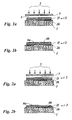
- FIG. 1a shows a carrier substrate 1, which in the exemplary embodiment shown is a banknote on which a multilayer body 2 is applied, which is formed from an adhesive layer 2k and a laminating layer 2l and, for example, as part of the transfer layer of a hot stamping foil Carrier substrate 1 is applied.
- the multilayer body 2 is designed as a transparent multilayer body, so that the multilayer body 2 releases the view of the carrier substrate 1 arranged below it.
- On the carrier substrate 1 facing away from the top of the lamination 21 is transferred by means of a gravure plate 3, an optical paint 4, which is introduced into depressions of the intaglio printing plate 3 is.
- the intaglio printing plate 3 is moved in the direction of the arrows 5 with a high contact pressure against a backing plate located behind the backing substrate and brought into contact with the lamination 2l, wherein the introduced into the wells of the intaglio printing plate 3 optical lacquer dissolves 4 of the wells and on the Top of the lamination 2l adheres. It forms in this way micro-optical structures 6a and 6b (FIG. 1b).
- the optical varnish 4 has a refractive index of about 1.5, because the micro-optical structures 6a and 6b formed by the varnish adjoin air.
- the micro-optical structure 6a is a microlens array
- the micro-optical structure 6b is an asymmetrical relief structure, for example a blazed grating.
- the microlens array may be provided to optically magnify a pictorial representation or alphanumeric characters printed on the carrier substrate.
- the blaze grating may be provided to form an interesting optical effect.
- the boundary contours of the Blaze grid can be designed, for example, as a logo or as an alphanumeric character.
- the intaglio printing plate 3 may be a plate-shaped body or a cylindrical body or a curved plate arranged on a printing cylinder. It can be provided that on a printing cylinder or the like more gravure plates are arranged, for example, register in the register with the micro-optical structures 6a and 6b color layers on the lamination 2, which may form, for example, a background pattern that partially or completely through the micro-optical structures 6a and 6b is covered.
- FIGS. 2a and 2b now show a second embodiment of the method according to the invention.
- FIG. 2 a shows the multilayer body 2 from FIG. 1 a, which is applied to the carrier substrate 1.
- the multilayer body 2 has the adhesive layer 2k and the laminating layer 2l.
- the intaglio printing plate 3 is now used only as an embossing tool with which the micro-optical structures 6a and 6b are molded into the laminating layer 2l under application pressure 5 (see FIG. 2b).
- the micro-optical Structures 6a and 6b may simultaneously constitute a tactile detectable security feature.
- FIGS. 3a to 3c now show a third embodiment of the method according to the invention.
- FIG. 3 a shows a multilayer body 32 that is applied to the carrier substrate 1.
- the multi-layer body 32 like the multi-layer body 2, has the adhesive layer 2k and the lamination layer 2l, on whose side facing away from the adhesive layer an optical lacquer layer 34 is applied.
- the optical structures 6a and 6b are molded by means of the intaglio printing plate 3 under contact pressure 5.
- the multilayer body 32 now has a protective layer 7 applied to the surface of the lacquer layer 34.
- the protective layer 7 is formed with a low refractive index, for example with a refractive index ⁇ 1.5, preferably with a refractive index ⁇ 1.
- the protective layer 7 is a normal resist having a refractive index of about 1.5 and applied by screen printing.
- the optical lacquer layer 34 advantageously has a high refractive index, for example> 1.9. It may be doped to form the high refractive index, for example with nanoparticles.
- the protective layer 7 increases the long-term stability of the molded in the lacquer layer 34 micro-optical structures 6a and 6b and protects them from contamination and / or wear.
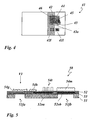
- a banknote 41 carries on its front side a film strip 42 having an OVD 42o and a latent image 42l.
- the latent image 42l is formed in this embodiment of interleaved Blazegittern, resulting in a tilted image.
- Another latent image 41l is executed as a color printed image and printed on the not covered by the film strip 42 surface of the banknote 41.
- the latent images 41l and 42l are in that shown in FIG. 4 illustrated embodiment arranged in alignment with each other in a spaced-apart.
- the latent image 42l shows the letter "O" and the latent image 41l shows the letter "K".
- the latent images are visible only at a predetermined viewing angle. They are invisible from all other points of view, ie latent.
- another OVD 43 is applied to the surface of the banknote 41 not covered by the film strip 42.
- the banknote 41 further has a microlens array 44, which is arranged above an image area 45 in the register.
- the OVDs 42o and 43 are also arranged in register with the microlens array 44 and are partially covered by the microlens array 44.
- any other security document can also be provided.
- the banknote 41 may optionally have a window 46, which projects at least partially into the region of the microlens array.
- a window bank note 50 shown in a schematic sectional view has a carrier substrate 51 which is formed with window-like openings 51fa and 51fb.
- the carrier substrate 51 may be, for example, a paper suitable for banknotes or a plastic film.
- a laminating layer 52 includes optically variable elements (OVD) 52oa and 52ob, which may be, for example, a KINEGRAM®.
- the KINEGRAM® can be fully metallised, demetallised or with a through the aspect ratio of the Surface reliefs may be carried out certain metallization, run with HRI layer or as a multilayer, or designed as a system with color change effects, and there may be a (crosslinked) liquid crystal layer integrated into the system.
- the OVD 52ob is arranged in the window opening 51fb and can therefore be viewed both in reflected light and in transmitted light.
- the OVD 52oa is disposed outside the window openings 51fa and 51fb, and therefore, can only be viewed in reflected light from the front of the sill 50.
- the laminating layer 52 may be formed as a transparent film or as a semitransparent film, for example as a colored film.
- the laminating layer 52 has on its underside an adhesive layer 53, by means of which it is connected to the carrier substrate 51.
- the adhesive layer may be a hot melt adhesive.
- the top of the laminating layer 52 is now printed with different security elements. It is a computer-generated hologram 54g provided with hidden information; a hologram 54h which can effectively represent, for example, alphanumeric characters such as a value impression; tactile features 54t, which may provide, for example, tactile information about the value of the bill; and a microlens array 54m, which in this embodiment is registered in register with the OVD 52ob disposed in the window aperture 51fb.
- the microlens array 54m when viewed from the front of the window banknote 50, produces an optically magnified image of the optical information stored in the OVD 52ob.
- the microlens array 54m when viewing the back side of the sill 50, the microlens array 54m is not optically effective, so that the optical information stored in the OVD 52ob appears to be all natural.
- the holograms 54g and 54h, the tactile feature 54t and the microlens array 54m are applied in intaglio pressure in one operation and therefore arranged in a strict register relative to one another.
- the microlens array 54m is deposited in register with the OVD 52ob, then the other printed elements are also in register with the OVD 52ob and any other elements incorporated in the register in the lamination layer, such as the OVD 52oa.
- the computer generated hologram 54g has pixel areas of different depths.
- the maximum pixel depth in the exemplary embodiment illustrated in FIG. 5 is 1 ⁇ m, the pixels have a size of 1 ⁇ m ⁇ 1 ⁇ m.
- the hidden information is encoded in the pixel depth, which causes a change in the phase angle of the incident light. For example, 8 to 256 different depths may be provided, i. Depending on the number of different depths in a pixel, information from 8 bits to 256 bits can be stored.
Landscapes
- Engineering & Computer Science (AREA)
- Manufacturing & Machinery (AREA)
- Credit Cards Or The Like (AREA)
- Printing Methods (AREA)
- Laminated Bodies (AREA)
Applications Claiming Priority (1)
| Application Number | Priority Date | Filing Date | Title |
|---|---|---|---|
| DE102006032660A DE102006032660A1 (de) | 2006-07-13 | 2006-07-13 | Mehrschichtkörper mit Mikrooptik |
Publications (4)
| Publication Number | Publication Date |
|---|---|
| EP1878584A2 true EP1878584A2 (fr) | 2008-01-16 |
| EP1878584A3 EP1878584A3 (fr) | 2008-07-23 |
| EP1878584B1 EP1878584B1 (fr) | 2014-04-30 |
| EP1878584B2 EP1878584B2 (fr) | 2019-10-23 |
Family
ID=38543781
Family Applications (1)
| Application Number | Title | Priority Date | Filing Date |
|---|---|---|---|
| EP07013569.4A Active EP1878584B2 (fr) | 2006-07-13 | 2007-07-11 | Corps multicouche à micro-optique |
Country Status (7)
| Country | Link |
|---|---|
| US (1) | US20080024846A1 (fr) |
| EP (1) | EP1878584B2 (fr) |
| CA (1) | CA2593340C (fr) |
| DE (1) | DE102006032660A1 (fr) |
| DK (1) | DK1878584T4 (fr) |
| ES (1) | ES2486341T5 (fr) |
| RU (1) | RU2435675C2 (fr) |
Cited By (10)
| Publication number | Priority date | Publication date | Assignee | Title |
|---|---|---|---|---|
| WO2009083146A2 (fr) * | 2007-12-21 | 2009-07-09 | Giesecke & Devrient Gmbh | Procédé de réalisation d'une microstructure |
| DE102008036482A1 (de) | 2008-08-05 | 2010-02-11 | Giesecke & Devrient Gmbh | Verfahren zum Herstellen von Mikrolinsen |
| WO2010054671A1 (fr) * | 2008-11-12 | 2010-05-20 | Nivatex Limited | Support de données à microcontours et son procédé de fabrication |
| WO2011015384A1 (fr) | 2009-08-04 | 2011-02-10 | Giesecke & Devrient Gmbh | Dispositif de sécurité |
| WO2011029602A3 (fr) * | 2009-09-11 | 2011-05-05 | Ovd Kinegram Ag | Corps multicouche |
| FR3030362A1 (fr) * | 2014-12-17 | 2016-06-24 | Oberthur Technologies | Dispositif de securite |
| EP3124285A1 (fr) * | 2015-07-27 | 2017-02-01 | Giesecke & Devrient GmbH | Outil d'estampage destine a fabriquer un element de securite ayant une structure optique variable |
| WO2018060308A1 (fr) * | 2016-09-29 | 2018-04-05 | Fraunhofer-Gesellschaft zur Förderung der angewandten Forschung e.V. | Unité d'accumulation d'énergie électrique à tôle de déflexion structurée et procédé pour structurer une tôle de déflexion d'une unité d'accumulation d'énergie électrique |
| EP3366474A1 (fr) | 2017-02-22 | 2018-08-29 | KBA-NotaSys SA | Presse à imprimer avec dispositif de coulée en ligne pour la réplication et la formation d'une structure micro-optique |
| WO2020177923A1 (fr) | 2019-03-06 | 2020-09-10 | Giesecke+Devrient Currency Technology Gmbh | Pigment de lentille, procédé de fabrication de celui-ci, document de valeur et encre d'impression |
Families Citing this family (15)
| Publication number | Priority date | Publication date | Assignee | Title |
|---|---|---|---|---|
| DE102009007779C5 (de) | 2009-02-04 | 2017-07-27 | Bundesdruckerei Gmbh | Verfahren zur Herstellung eines ohne technische Hilfsmittel visuell wahrnehmbaren Sicherheitsmerkmals, Sicherheitsmerkmal für kunststoffbasierendes Wert- oder Sicherheitsdokument sowie Dokument mit wenigstens einem solchen Sicherheitsmerkmal |
| DE102010019766A1 (de) * | 2010-05-07 | 2011-11-10 | Giesecke & Devrient Gmbh | Verfahren zur Erzeugung einer Mikrostruktur auf einem Träger |
| RU2480550C1 (ru) * | 2011-12-23 | 2013-04-27 | Федеральное Государственное Унитарное Предприятие "Гознак" (Фгуп "Гознак") | Полимерный многослойный комбинированный защитный элемент и способ его изготовления |
| DE102012204340A1 (de) * | 2012-03-19 | 2013-09-19 | Bundesdruckerei Gmbh | Sicherheitsdokument mit einem Perforationsfenster und Verfahren zu dessen Herstellung |
| GB201208137D0 (en) * | 2012-05-10 | 2012-06-20 | Rue De Int Ltd | Security devices and methods of manufacture therefor |
| CN103847289B (zh) * | 2012-11-29 | 2016-03-23 | 中钞特种防伪科技有限公司 | 具有再现隐藏图像的光学防伪元件及用其制成的产品 |
| DE102013016775A1 (de) * | 2013-10-09 | 2015-04-09 | Giesecke & Devrient Gmbh | Verfahren zur Herstellung eines tragbaren Datenträgers |
| DE102013016776A1 (de) * | 2013-10-09 | 2015-04-09 | Giesecke & Devrient Gmbh | Verfahren zur Herstellung einer Linsenstruktur |
| DE102014018512A1 (de) | 2014-12-12 | 2016-06-16 | Giesecke & Devrient Gmbh | Optisch variables Sicherheitselement |
| US20170123112A1 (en) * | 2015-10-28 | 2017-05-04 | Joel Scott Scarbrough | Multilayered Press Stable Lens Array Film |
| GB2580069B (en) * | 2018-12-20 | 2022-06-15 | De La Rue Int Ltd | Security documents and methods of manufacture thereof |
| DE102019111647A1 (de) * | 2019-05-06 | 2020-11-12 | HELLA GmbH & Co. KGaA | Beleuchtungsvorrichtung für ein Fahrzeug sowie Verfahren zur Herstellung einer Beleuchtungsvorrichtung für ein Fahrzeug |
| AU2020279844A1 (en) | 2019-05-20 | 2021-12-23 | Crane & Co., Inc. | Use of nanoparticles to tune index of refraction of layers of a polymeric matrix to optimize microoptic (MO) focus |
| PL3888929T3 (pl) | 2020-03-31 | 2023-01-16 | Pentacomp Pte. Ltd. | Sposób wytwarzania dyskretyzowanej optycznej mikrostruktury zabezpieczającej na podłożu i podkładka do stosowania w tym sposobie |
| AU2021339052A1 (en) * | 2020-09-11 | 2023-04-13 | De La Rue International Limited | Security devices and methods of manufacture thereof |
Citations (2)
| Publication number | Priority date | Publication date | Assignee | Title |
|---|---|---|---|---|
| EP0429782A1 (fr) | 1989-12-01 | 1991-06-05 | Landis & Gyr Technology Innovation AG | Dispositif pour modifier la protection contre la falsification d'un document de valeur |
| WO2002091041A1 (fr) | 2001-05-08 | 2002-11-14 | Commonwealth Scientific And Industrial Research Organisation | Dispositif optique et ses procedes de fabrication |
Family Cites Families (14)
| Publication number | Priority date | Publication date | Assignee | Title |
|---|---|---|---|---|
| US5105125A (en) * | 1990-08-06 | 1992-04-14 | Yang Tai Her | Device for alternating bulb polarities of a DC lighting system |
| GB9309673D0 (en) * | 1993-05-11 | 1993-06-23 | De La Rue Holographics Ltd | Security device |
| AUPO484797A0 (en) * | 1997-01-29 | 1997-02-20 | Securency Pty Ltd | Printed matter producing reflective intaglio effect |
| DE10008851A1 (de) * | 2000-02-25 | 2001-08-30 | Giesecke & Devrient Gmbh | Verfahren zur Herstellung laserbeschriftbarer Datenträger und damit hergestellte Datenträger |
| DE10032128A1 (de) * | 2000-07-05 | 2002-01-17 | Giesecke & Devrient Gmbh | Sicherheitspapier und daraus hergestelltes Wertdokument |
| US7357077B2 (en) * | 2000-09-08 | 2008-04-15 | Giesecke & Devrient Gmbh | Data carrier, method for the production thereof and gravure printing plate |
| DE10201032A1 (de) * | 2002-01-11 | 2003-07-24 | Giesecke & Devrient Gmbh | Stahltiefdruckverfahren zum Herstellen eines Sicherheitsdokuments sowie Stahltiefdruckplatte und Halbzeuge dafür und Verfahren zu deren Herstellung |
| CA2405249A1 (fr) * | 2002-09-24 | 2004-03-24 | Canadian Bank Note Company, Limited | Dispositif et methode de securite par impression |
| JP4391102B2 (ja) * | 2002-10-01 | 2009-12-24 | 大日本印刷株式会社 | 真偽判定体 |
| CA2501478A1 (fr) * | 2002-10-07 | 2004-04-15 | Note Printing Australia Limited | Dispositifs estampes a couleurs changeantes |
| JP4170774B2 (ja) * | 2003-01-09 | 2008-10-22 | 大日本印刷株式会社 | 真偽判定体用転写箔 |
| JP4304001B2 (ja) * | 2003-05-22 | 2009-07-29 | 大日本印刷株式会社 | 真偽判定体 |
| GB0401370D0 (en) † | 2004-01-21 | 2004-02-25 | Rue De Int Ltd | Security device |
| SI1765600T1 (sl) * | 2004-06-30 | 2009-06-30 | Kxo Ag | Pred ponarejanjem varen zavarovani predmet in postopek za njegovo izdelavo ter verifikacijo |
-
2006
- 2006-07-13 DE DE102006032660A patent/DE102006032660A1/de not_active Withdrawn
-
2007
- 2007-07-10 CA CA2593340A patent/CA2593340C/fr active Active
- 2007-07-11 EP EP07013569.4A patent/EP1878584B2/fr active Active
- 2007-07-11 DK DK07013569.4T patent/DK1878584T4/da active
- 2007-07-11 ES ES07013569T patent/ES2486341T5/es active Active
- 2007-07-12 RU RU2007126660/12A patent/RU2435675C2/ru active
- 2007-07-12 US US11/827,453 patent/US20080024846A1/en not_active Abandoned
Patent Citations (2)
| Publication number | Priority date | Publication date | Assignee | Title |
|---|---|---|---|---|
| EP0429782A1 (fr) | 1989-12-01 | 1991-06-05 | Landis & Gyr Technology Innovation AG | Dispositif pour modifier la protection contre la falsification d'un document de valeur |
| WO2002091041A1 (fr) | 2001-05-08 | 2002-11-14 | Commonwealth Scientific And Industrial Research Organisation | Dispositif optique et ses procedes de fabrication |
Cited By (26)
| Publication number | Priority date | Publication date | Assignee | Title |
|---|---|---|---|---|
| US8685488B2 (en) | 2007-12-21 | 2014-04-01 | Giesecke & Devrient Gmbh | Method for producing a microstructure |
| WO2009083146A3 (fr) * | 2007-12-21 | 2009-12-30 | Giesecke & Devrient Gmbh | Procédé de réalisation d'une microstructure |
| WO2009083146A2 (fr) * | 2007-12-21 | 2009-07-09 | Giesecke & Devrient Gmbh | Procédé de réalisation d'une microstructure |
| DE102008036482A1 (de) | 2008-08-05 | 2010-02-11 | Giesecke & Devrient Gmbh | Verfahren zum Herstellen von Mikrolinsen |
| WO2010054671A1 (fr) * | 2008-11-12 | 2010-05-20 | Nivatex Limited | Support de données à microcontours et son procédé de fabrication |
| WO2011015384A1 (fr) | 2009-08-04 | 2011-02-10 | Giesecke & Devrient Gmbh | Dispositif de sécurité |
| CN102497995A (zh) * | 2009-09-11 | 2012-06-13 | Ovd基尼格拉姆股份公司 | 多层体 |
| JP2013504451A (ja) * | 2009-09-11 | 2013-02-07 | オーファウデー キネグラム アーゲー | 多層体 |
| US9994062B2 (en) | 2009-09-11 | 2018-06-12 | Ovd Kinegram Ag | Multilayer body |
| RU2549069C2 (ru) * | 2009-09-11 | 2015-04-20 | Овд Кинеграм Аг | Многослойное тело защитного элемента для защиты ценных документов |
| CN102497995B (zh) * | 2009-09-11 | 2015-09-09 | Ovd基尼格拉姆股份公司 | 多层体 |
| WO2011029602A3 (fr) * | 2009-09-11 | 2011-05-05 | Ovd Kinegram Ag | Corps multicouche |
| US11077700B2 (en) | 2009-09-11 | 2021-08-03 | Ovd Kinegram Ag | Multilayer body |
| FR3030362A1 (fr) * | 2014-12-17 | 2016-06-24 | Oberthur Technologies | Dispositif de securite |
| EP3124285A1 (fr) * | 2015-07-27 | 2017-02-01 | Giesecke & Devrient GmbH | Outil d'estampage destine a fabriquer un element de securite ayant une structure optique variable |
| EP3124285B1 (fr) | 2015-07-27 | 2020-06-17 | Giesecke+Devrient Currency Technology GmbH | Outil d'estampage destine a fabriquer un element de securite ayant une structure optique variable |
| WO2018060308A1 (fr) * | 2016-09-29 | 2018-04-05 | Fraunhofer-Gesellschaft zur Förderung der angewandten Forschung e.V. | Unité d'accumulation d'énergie électrique à tôle de déflexion structurée et procédé pour structurer une tôle de déflexion d'une unité d'accumulation d'énergie électrique |
| EP3366474A1 (fr) | 2017-02-22 | 2018-08-29 | KBA-NotaSys SA | Presse à imprimer avec dispositif de coulée en ligne pour la réplication et la formation d'une structure micro-optique |
| EP3366475A1 (fr) | 2017-02-22 | 2018-08-29 | KBA-NotaSys SA | Presse à imprimer ayant un dispositif de coulée en ligne pour la réplication et la formation d'une structure micro-optique |
| WO2018153839A1 (fr) | 2017-02-22 | 2018-08-30 | Kba-Notasys Sa | Presse à imprimer avec dispositif de coulée en ligne permettant la duplication et la formation d'une structure micro-optique |
| WO2018153840A1 (fr) | 2017-02-22 | 2018-08-30 | Kba-Notasys Sa | Presse à imprimer avec dispositif de coulée en ligne pour la réplication et la formation d'une structure micro-optique |
| AU2018223136B2 (en) * | 2017-02-22 | 2019-08-22 | De La Rue International Limited | Printing press with in-line casting device for the replication and formation of a micro-optical structure |
| US11383507B2 (en) | 2017-02-22 | 2022-07-12 | Kba-Notasys Sa | Printing press with in-line casting device for the replication and formation of a micro-optical structure |
| US11772374B2 (en) | 2017-02-22 | 2023-10-03 | Kba-Notasys Sa | Printing press with in-line casting device for the replication and formation of a micro-optical structure |
| WO2020177923A1 (fr) | 2019-03-06 | 2020-09-10 | Giesecke+Devrient Currency Technology Gmbh | Pigment de lentille, procédé de fabrication de celui-ci, document de valeur et encre d'impression |
| US11618276B2 (en) | 2019-03-06 | 2023-04-04 | Giesecke+Devrient Currency Technology Gmbh | Lens pigment, method for producing the same, valuable document and printing ink |
Also Published As
| Publication number | Publication date |
|---|---|
| CA2593340A1 (fr) | 2008-01-13 |
| EP1878584B2 (fr) | 2019-10-23 |
| RU2007126660A (ru) | 2009-01-20 |
| DK1878584T4 (da) | 2020-02-03 |
| EP1878584B1 (fr) | 2014-04-30 |
| RU2435675C2 (ru) | 2011-12-10 |
| US20080024846A1 (en) | 2008-01-31 |
| ES2486341T3 (es) | 2014-08-18 |
| EP1878584A3 (fr) | 2008-07-23 |
| DK1878584T3 (da) | 2014-07-07 |
| ES2486341T5 (es) | 2020-05-22 |
| CA2593340C (fr) | 2015-10-20 |
| DE102006032660A1 (de) | 2008-01-17 |
Similar Documents
| Publication | Publication Date | Title |
|---|---|---|
| EP1878584B1 (fr) | Méthode pour la fabrication d'un corps multicouche à micro-optique | |
| EP3216620B1 (fr) | Élement de securite, document de valeur dote d'un tel element de securite ainsi que procede de fabrication d'un element de securite | |
| EP1966769B2 (fr) | Elément de sécurité à variation d'aspect et son procédé de fabrication | |
| EP1853763B1 (fr) | Element de securite et procede de production de cet element | |
| EP1747100B1 (fr) | Element de securite se presentant sous la forme d'un corps en pellicule multicouche | |
| EP1786632B2 (fr) | Element de securite metallise | |
| EP2303594B1 (fr) | Élément de sécurité | |
| EP1800271B1 (fr) | Document de securite | |
| EP2225110B1 (fr) | Élément de sécurité | |
| CH704944B1 (de) | Sicherheitsdokument mit integrierter Sicherheitsvorrichtung und Herstellungsverfahren. | |
| DE102008036482A1 (de) | Verfahren zum Herstellen von Mikrolinsen | |
| DE112011102365T5 (de) | Optisch variable Einrichtung | |
| DE102006050047A1 (de) | Durchsichtssicherheitselement mit Mikrostrukturen | |
| DE112017001373T5 (de) | Mikrooptische Vorrichtung mit doppelseitigem optischem Effekt | |
| EP3750717B1 (fr) | Procédé de fabrication d'un élément de sécurité ainsi qu'un élément de sécurité | |
| EP2768660B1 (fr) | Procédé de réalisation de micro-miroirs creux | |
| EP3034315B1 (fr) | Élement de securite, son procede de fabrication et support de donnees dote d'un element de securite | |
| EP2593310B1 (fr) | Élément de sécurité et structures d'hologrammes | |
| DE112021000368T5 (de) | Optische effekte erzeugende vorrichtung | |
| EP3406458A1 (fr) | Élément de sécurité à zone de surface réfléchissante | |
| DE112017003672T5 (de) | Prägewerkzeug und Verfahren zur Minimierung der Blasenbildung in Prägestrukturen |
Legal Events
| Date | Code | Title | Description |
|---|---|---|---|
| PUAI | Public reference made under article 153(3) epc to a published international application that has entered the european phase |
Free format text: ORIGINAL CODE: 0009012 |
|
| AK | Designated contracting states |
Kind code of ref document: A2 Designated state(s): AT BE BG CH CY CZ DE DK EE ES FI FR GB GR HU IE IS IT LI LT LU LV MC MT NL PL PT RO SE SI SK TR |
|
| AX | Request for extension of the european patent |
Extension state: AL BA HR MK YU |
|
| PUAL | Search report despatched |
Free format text: ORIGINAL CODE: 0009013 |
|
| AK | Designated contracting states |
Kind code of ref document: A3 Designated state(s): AT BE BG CH CY CZ DE DK EE ES FI FR GB GR HU IE IS IT LI LT LU LV MC MT NL PL PT RO SE SI SK TR |
|
| AX | Request for extension of the european patent |
Extension state: AL BA HR MK RS |
|
| 17P | Request for examination filed |
Effective date: 20090122 |
|
| 17Q | First examination report despatched |
Effective date: 20090226 |
|
| AKX | Designation fees paid |
Designated state(s): AT BE BG CH CY CZ DE DK EE ES FI FR GB GR HU IE IS IT LI LT LU LV MC MT NL PL PT RO SE SI SK TR |
|
| R17C | First examination report despatched (corrected) |
Effective date: 20090226 |
|
| RAP1 | Party data changed (applicant data changed or rights of an application transferred) |
Owner name: OVD KINEGRAM AG Owner name: KBA-GIORI S.A. |
|
| RAP1 | Party data changed (applicant data changed or rights of an application transferred) |
Owner name: KBA-NOTASYS SA Owner name: OVD KINEGRAM AG |
|
| REG | Reference to a national code |
Ref country code: DE Ref legal event code: R079 Ref document number: 502007013033 Country of ref document: DE Free format text: PREVIOUS MAIN CLASS: B41M0001100000 Ipc: B41M0003140000 |
|
| GRAP | Despatch of communication of intention to grant a patent |
Free format text: ORIGINAL CODE: EPIDOSNIGR1 |
|
| RIC1 | Information provided on ipc code assigned before grant |
Ipc: B41M 3/14 20060101AFI20131031BHEP Ipc: B41M 1/10 20060101ALI20131031BHEP |
|
| INTG | Intention to grant announced |
Effective date: 20131128 |
|
| GRAS | Grant fee paid |
Free format text: ORIGINAL CODE: EPIDOSNIGR3 |
|
| GRAA | (expected) grant |
Free format text: ORIGINAL CODE: 0009210 |
|
| AK | Designated contracting states |
Kind code of ref document: B1 Designated state(s): AT BE BG CH CY CZ DE DK EE ES FI FR GB GR HU IE IS IT LI LT LU LV MC MT NL PL PT RO SE SI SK TR |
|
| REG | Reference to a national code |
Ref country code: GB Ref legal event code: FG4D Free format text: NOT ENGLISH Ref country code: CH Ref legal event code: EP |
|
| REG | Reference to a national code |
Ref country code: AT Ref legal event code: REF Ref document number: 664830 Country of ref document: AT Kind code of ref document: T Effective date: 20140515 |
|
| REG | Reference to a national code |
Ref country code: IE Ref legal event code: FG4D Free format text: LANGUAGE OF EP DOCUMENT: GERMAN |
|
| REG | Reference to a national code |
Ref country code: CH Ref legal event code: NV Representative=s name: FIAMMENGHI-FIAMMENGHI, CH |
|
| REG | Reference to a national code |
Ref country code: DE Ref legal event code: R096 Ref document number: 502007013033 Country of ref document: DE Effective date: 20140612 |
|
| REG | Reference to a national code |
Ref country code: DK Ref legal event code: T3 Effective date: 20140704 Ref country code: RO Ref legal event code: EPE |
|
| REG | Reference to a national code |
Ref country code: SE Ref legal event code: TRGR |
|
| REG | Reference to a national code |
Ref country code: ES Ref legal event code: FG2A Ref document number: 2486341 Country of ref document: ES Kind code of ref document: T3 Effective date: 20140818 |
|
| REG | Reference to a national code |
Ref country code: LT Ref legal event code: MG4D |
|
| REG | Reference to a national code |
Ref country code: NL Ref legal event code: VDEP Effective date: 20140430 |
|
| PG25 | Lapsed in a contracting state [announced via postgrant information from national office to epo] |
Ref country code: CY Free format text: LAPSE BECAUSE OF FAILURE TO SUBMIT A TRANSLATION OF THE DESCRIPTION OR TO PAY THE FEE WITHIN THE PRESCRIBED TIME-LIMIT Effective date: 20140430 Ref country code: FI Free format text: LAPSE BECAUSE OF FAILURE TO SUBMIT A TRANSLATION OF THE DESCRIPTION OR TO PAY THE FEE WITHIN THE PRESCRIBED TIME-LIMIT Effective date: 20140430 Ref country code: IS Free format text: LAPSE BECAUSE OF FAILURE TO SUBMIT A TRANSLATION OF THE DESCRIPTION OR TO PAY THE FEE WITHIN THE PRESCRIBED TIME-LIMIT Effective date: 20140830 Ref country code: BG Free format text: LAPSE BECAUSE OF FAILURE TO SUBMIT A TRANSLATION OF THE DESCRIPTION OR TO PAY THE FEE WITHIN THE PRESCRIBED TIME-LIMIT Effective date: 20140730 Ref country code: NL Free format text: LAPSE BECAUSE OF FAILURE TO SUBMIT A TRANSLATION OF THE DESCRIPTION OR TO PAY THE FEE WITHIN THE PRESCRIBED TIME-LIMIT Effective date: 20140430 Ref country code: LT Free format text: LAPSE BECAUSE OF FAILURE TO SUBMIT A TRANSLATION OF THE DESCRIPTION OR TO PAY THE FEE WITHIN THE PRESCRIBED TIME-LIMIT Effective date: 20140430 Ref country code: GR Free format text: LAPSE BECAUSE OF FAILURE TO SUBMIT A TRANSLATION OF THE DESCRIPTION OR TO PAY THE FEE WITHIN THE PRESCRIBED TIME-LIMIT Effective date: 20140731 |
|
| PG25 | Lapsed in a contracting state [announced via postgrant information from national office to epo] |
Ref country code: LV Free format text: LAPSE BECAUSE OF FAILURE TO SUBMIT A TRANSLATION OF THE DESCRIPTION OR TO PAY THE FEE WITHIN THE PRESCRIBED TIME-LIMIT Effective date: 20140430 Ref country code: PL Free format text: LAPSE BECAUSE OF FAILURE TO SUBMIT A TRANSLATION OF THE DESCRIPTION OR TO PAY THE FEE WITHIN THE PRESCRIBED TIME-LIMIT Effective date: 20140430 |
|
| PG25 | Lapsed in a contracting state [announced via postgrant information from national office to epo] |
Ref country code: PT Free format text: LAPSE BECAUSE OF FAILURE TO SUBMIT A TRANSLATION OF THE DESCRIPTION OR TO PAY THE FEE WITHIN THE PRESCRIBED TIME-LIMIT Effective date: 20140901 |
|
| REG | Reference to a national code |
Ref country code: DE Ref legal event code: R026 Ref document number: 502007013033 Country of ref document: DE |
|
| PG25 | Lapsed in a contracting state [announced via postgrant information from national office to epo] |
Ref country code: SK Free format text: LAPSE BECAUSE OF FAILURE TO SUBMIT A TRANSLATION OF THE DESCRIPTION OR TO PAY THE FEE WITHIN THE PRESCRIBED TIME-LIMIT Effective date: 20140430 Ref country code: CZ Free format text: LAPSE BECAUSE OF FAILURE TO SUBMIT A TRANSLATION OF THE DESCRIPTION OR TO PAY THE FEE WITHIN THE PRESCRIBED TIME-LIMIT Effective date: 20140430 Ref country code: EE Free format text: LAPSE BECAUSE OF FAILURE TO SUBMIT A TRANSLATION OF THE DESCRIPTION OR TO PAY THE FEE WITHIN THE PRESCRIBED TIME-LIMIT Effective date: 20140430 |
|
| PLBI | Opposition filed |
Free format text: ORIGINAL CODE: 0009260 |
|
| PG25 | Lapsed in a contracting state [announced via postgrant information from national office to epo] |
Ref country code: LU Free format text: LAPSE BECAUSE OF FAILURE TO SUBMIT A TRANSLATION OF THE DESCRIPTION OR TO PAY THE FEE WITHIN THE PRESCRIBED TIME-LIMIT Effective date: 20140711 |
|
| PLAX | Notice of opposition and request to file observation + time limit sent |
Free format text: ORIGINAL CODE: EPIDOSNOBS2 |
|
| 26 | Opposition filed |
Opponent name: GIESECKE & DEVRIENT GMBH Effective date: 20150129 |
|
| PG25 | Lapsed in a contracting state [announced via postgrant information from national office to epo] |
Ref country code: IT Free format text: LAPSE BECAUSE OF FAILURE TO SUBMIT A TRANSLATION OF THE DESCRIPTION OR TO PAY THE FEE WITHIN THE PRESCRIBED TIME-LIMIT Effective date: 20140430 |
|
| REG | Reference to a national code |
Ref country code: DE Ref legal event code: R026 Ref document number: 502007013033 Country of ref document: DE Effective date: 20150129 |
|
| REG | Reference to a national code |
Ref country code: IE Ref legal event code: MM4A |
|
| PLAF | Information modified related to communication of a notice of opposition and request to file observations + time limit |
Free format text: ORIGINAL CODE: EPIDOSCOBS2 |
|
| PG25 | Lapsed in a contracting state [announced via postgrant information from national office to epo] |
Ref country code: SI Free format text: LAPSE BECAUSE OF FAILURE TO SUBMIT A TRANSLATION OF THE DESCRIPTION OR TO PAY THE FEE WITHIN THE PRESCRIBED TIME-LIMIT Effective date: 20140430 |
|
| PG25 | Lapsed in a contracting state [announced via postgrant information from national office to epo] |
Ref country code: IE Free format text: LAPSE BECAUSE OF NON-PAYMENT OF DUE FEES Effective date: 20140711 |
|
| REG | Reference to a national code |
Ref country code: AT Ref legal event code: MM01 Ref document number: 664830 Country of ref document: AT Kind code of ref document: T Effective date: 20140711 |
|
| PLBB | Reply of patent proprietor to notice(s) of opposition received |
Free format text: ORIGINAL CODE: EPIDOSNOBS3 |
|
| PG25 | Lapsed in a contracting state [announced via postgrant information from national office to epo] |
Ref country code: AT Free format text: LAPSE BECAUSE OF NON-PAYMENT OF DUE FEES Effective date: 20140711 |
|
| PG25 | Lapsed in a contracting state [announced via postgrant information from national office to epo] |
Ref country code: MC Free format text: LAPSE BECAUSE OF FAILURE TO SUBMIT A TRANSLATION OF THE DESCRIPTION OR TO PAY THE FEE WITHIN THE PRESCRIBED TIME-LIMIT Effective date: 20140430 |
|
| PG25 | Lapsed in a contracting state [announced via postgrant information from national office to epo] |
Ref country code: MT Free format text: LAPSE BECAUSE OF FAILURE TO SUBMIT A TRANSLATION OF THE DESCRIPTION OR TO PAY THE FEE WITHIN THE PRESCRIBED TIME-LIMIT Effective date: 20140430 |
|
| REG | Reference to a national code |
Ref country code: FR Ref legal event code: PLFP Year of fee payment: 10 |
|
| PG25 | Lapsed in a contracting state [announced via postgrant information from national office to epo] |
Ref country code: BE Free format text: LAPSE BECAUSE OF FAILURE TO SUBMIT A TRANSLATION OF THE DESCRIPTION OR TO PAY THE FEE WITHIN THE PRESCRIBED TIME-LIMIT Effective date: 20140731 Ref country code: HU Free format text: LAPSE BECAUSE OF FAILURE TO SUBMIT A TRANSLATION OF THE DESCRIPTION OR TO PAY THE FEE WITHIN THE PRESCRIBED TIME-LIMIT; INVALID AB INITIO Effective date: 20070711 |
|
| REG | Reference to a national code |
Ref country code: FR Ref legal event code: PLFP Year of fee payment: 11 |
|
| PLBP | Opposition withdrawn |
Free format text: ORIGINAL CODE: 0009264 |
|
| REG | Reference to a national code |
Ref country code: FR Ref legal event code: PLFP Year of fee payment: 12 |
|
| REG | Reference to a national code |
Ref country code: CH Ref legal event code: PK Free format text: BERICHTIGUNGEN |
|
| RAP2 | Party data changed (patent owner data changed or rights of a patent transferred) |
Owner name: OVD KINEGRAM AG Owner name: KBA-NOTASYS SA |
|
| RIC2 | Information provided on ipc code assigned after grant |
Ipc: B41M 3/14 20060101AFI20190527BHEP Ipc: B41M 1/10 20060101ALI20190527BHEP Ipc: B42D 25/00 20140101ALI20190527BHEP |
|
| PUAH | Patent maintained in amended form |
Free format text: ORIGINAL CODE: 0009272 |
|
| STAA | Information on the status of an ep patent application or granted ep patent |
Free format text: STATUS: PATENT MAINTAINED AS AMENDED |
|
| REG | Reference to a national code |
Ref country code: CH Ref legal event code: AELC |
|
| 27A | Patent maintained in amended form |
Effective date: 20191023 |
|
| AK | Designated contracting states |
Kind code of ref document: B2 Designated state(s): AT BE BG CH CY CZ DE DK EE ES FI FR GB GR HU IE IS IT LI LT LU LV MC MT NL PL PT RO SE SI SK TR |
|
| REG | Reference to a national code |
Ref country code: DE Ref legal event code: R102 Ref document number: 502007013033 Country of ref document: DE |
|
| REG | Reference to a national code |
Ref country code: SE Ref legal event code: RPEO |
|
| REG | Reference to a national code |
Ref country code: DK Ref legal event code: T4 Effective date: 20200129 |
|
| REG | Reference to a national code |
Ref country code: ES Ref legal event code: DC2A Ref document number: 2486341 Country of ref document: ES Kind code of ref document: T5 Effective date: 20200522 |
|
| PGFP | Annual fee paid to national office [announced via postgrant information from national office to epo] |
Ref country code: TR Payment date: 20220704 Year of fee payment: 16 Ref country code: SE Payment date: 20220721 Year of fee payment: 16 Ref country code: RO Payment date: 20220701 Year of fee payment: 16 Ref country code: GB Payment date: 20220725 Year of fee payment: 16 Ref country code: ES Payment date: 20220819 Year of fee payment: 16 Ref country code: DK Payment date: 20220721 Year of fee payment: 16 |
|
| PGFP | Annual fee paid to national office [announced via postgrant information from national office to epo] |
Ref country code: FR Payment date: 20220725 Year of fee payment: 16 |
|
| PGFP | Annual fee paid to national office [announced via postgrant information from national office to epo] |
Ref country code: CH Payment date: 20230801 Year of fee payment: 17 |
|
| PGFP | Annual fee paid to national office [announced via postgrant information from national office to epo] |
Ref country code: DE Payment date: 20230622 Year of fee payment: 17 |
|
| REG | Reference to a national code |
Ref country code: DK Ref legal event code: EBP Effective date: 20230731 |
|
| REG | Reference to a national code |
Ref country code: SE Ref legal event code: EUG |
|
| GBPC | Gb: european patent ceased through non-payment of renewal fee |
Effective date: 20230711 |
|
| PG25 | Lapsed in a contracting state [announced via postgrant information from national office to epo] |
Ref country code: RO Free format text: LAPSE BECAUSE OF NON-PAYMENT OF DUE FEES Effective date: 20230711 Ref country code: GB Free format text: LAPSE BECAUSE OF NON-PAYMENT OF DUE FEES Effective date: 20230711 |