EP1876582A2 - Organic light emitting display and driving method thereof - Google Patents
Organic light emitting display and driving method thereof Download PDFInfo
- Publication number
- EP1876582A2 EP1876582A2 EP07251686A EP07251686A EP1876582A2 EP 1876582 A2 EP1876582 A2 EP 1876582A2 EP 07251686 A EP07251686 A EP 07251686A EP 07251686 A EP07251686 A EP 07251686A EP 1876582 A2 EP1876582 A2 EP 1876582A2
- Authority
- EP
- European Patent Office
- Prior art keywords
- drive current
- column lines
- period
- drive
- light emitting
- Prior art date
- Legal status (The legal status is an assumption and is not a legal conclusion. Google has not performed a legal analysis and makes no representation as to the accuracy of the status listed.)
- Withdrawn
Links
Images
Classifications
-
- G—PHYSICS
- G09—EDUCATION; CRYPTOGRAPHY; DISPLAY; ADVERTISING; SEALS
- G09G—ARRANGEMENTS OR CIRCUITS FOR CONTROL OF INDICATING DEVICES USING STATIC MEANS TO PRESENT VARIABLE INFORMATION
- G09G3/00—Control arrangements or circuits, of interest only in connection with visual indicators other than cathode-ray tubes
- G09G3/20—Control arrangements or circuits, of interest only in connection with visual indicators other than cathode-ray tubes for presentation of an assembly of a number of characters, e.g. a page, by composing the assembly by combination of individual elements arranged in a matrix no fixed position being assigned to or needed to be assigned to the individual characters or partial characters
- G09G3/22—Control arrangements or circuits, of interest only in connection with visual indicators other than cathode-ray tubes for presentation of an assembly of a number of characters, e.g. a page, by composing the assembly by combination of individual elements arranged in a matrix no fixed position being assigned to or needed to be assigned to the individual characters or partial characters using controlled light sources
- G09G3/30—Control arrangements or circuits, of interest only in connection with visual indicators other than cathode-ray tubes for presentation of an assembly of a number of characters, e.g. a page, by composing the assembly by combination of individual elements arranged in a matrix no fixed position being assigned to or needed to be assigned to the individual characters or partial characters using controlled light sources using electroluminescent panels
- G09G3/32—Control arrangements or circuits, of interest only in connection with visual indicators other than cathode-ray tubes for presentation of an assembly of a number of characters, e.g. a page, by composing the assembly by combination of individual elements arranged in a matrix no fixed position being assigned to or needed to be assigned to the individual characters or partial characters using controlled light sources using electroluminescent panels semiconductive, e.g. using light-emitting diodes [LED]
- G09G3/3208—Control arrangements or circuits, of interest only in connection with visual indicators other than cathode-ray tubes for presentation of an assembly of a number of characters, e.g. a page, by composing the assembly by combination of individual elements arranged in a matrix no fixed position being assigned to or needed to be assigned to the individual characters or partial characters using controlled light sources using electroluminescent panels semiconductive, e.g. using light-emitting diodes [LED] organic, e.g. using organic light-emitting diodes [OLED]
- G09G3/3275—Details of drivers for data electrodes
- G09G3/3283—Details of drivers for data electrodes in which the data driver supplies a variable data current for setting the current through, or the voltage across, the light-emitting elements
-
- G—PHYSICS
- G09—EDUCATION; CRYPTOGRAPHY; DISPLAY; ADVERTISING; SEALS
- G09G—ARRANGEMENTS OR CIRCUITS FOR CONTROL OF INDICATING DEVICES USING STATIC MEANS TO PRESENT VARIABLE INFORMATION
- G09G3/00—Control arrangements or circuits, of interest only in connection with visual indicators other than cathode-ray tubes
- G09G3/20—Control arrangements or circuits, of interest only in connection with visual indicators other than cathode-ray tubes for presentation of an assembly of a number of characters, e.g. a page, by composing the assembly by combination of individual elements arranged in a matrix no fixed position being assigned to or needed to be assigned to the individual characters or partial characters
- G09G3/22—Control arrangements or circuits, of interest only in connection with visual indicators other than cathode-ray tubes for presentation of an assembly of a number of characters, e.g. a page, by composing the assembly by combination of individual elements arranged in a matrix no fixed position being assigned to or needed to be assigned to the individual characters or partial characters using controlled light sources
- G09G3/30—Control arrangements or circuits, of interest only in connection with visual indicators other than cathode-ray tubes for presentation of an assembly of a number of characters, e.g. a page, by composing the assembly by combination of individual elements arranged in a matrix no fixed position being assigned to or needed to be assigned to the individual characters or partial characters using controlled light sources using electroluminescent panels
-
- G—PHYSICS
- G09—EDUCATION; CRYPTOGRAPHY; DISPLAY; ADVERTISING; SEALS
- G09G—ARRANGEMENTS OR CIRCUITS FOR CONTROL OF INDICATING DEVICES USING STATIC MEANS TO PRESENT VARIABLE INFORMATION
- G09G3/00—Control arrangements or circuits, of interest only in connection with visual indicators other than cathode-ray tubes
- G09G3/20—Control arrangements or circuits, of interest only in connection with visual indicators other than cathode-ray tubes for presentation of an assembly of a number of characters, e.g. a page, by composing the assembly by combination of individual elements arranged in a matrix no fixed position being assigned to or needed to be assigned to the individual characters or partial characters
-
- G—PHYSICS
- G09—EDUCATION; CRYPTOGRAPHY; DISPLAY; ADVERTISING; SEALS
- G09G—ARRANGEMENTS OR CIRCUITS FOR CONTROL OF INDICATING DEVICES USING STATIC MEANS TO PRESENT VARIABLE INFORMATION
- G09G3/00—Control arrangements or circuits, of interest only in connection with visual indicators other than cathode-ray tubes
- G09G3/20—Control arrangements or circuits, of interest only in connection with visual indicators other than cathode-ray tubes for presentation of an assembly of a number of characters, e.g. a page, by composing the assembly by combination of individual elements arranged in a matrix no fixed position being assigned to or needed to be assigned to the individual characters or partial characters
- G09G3/22—Control arrangements or circuits, of interest only in connection with visual indicators other than cathode-ray tubes for presentation of an assembly of a number of characters, e.g. a page, by composing the assembly by combination of individual elements arranged in a matrix no fixed position being assigned to or needed to be assigned to the individual characters or partial characters using controlled light sources
- G09G3/30—Control arrangements or circuits, of interest only in connection with visual indicators other than cathode-ray tubes for presentation of an assembly of a number of characters, e.g. a page, by composing the assembly by combination of individual elements arranged in a matrix no fixed position being assigned to or needed to be assigned to the individual characters or partial characters using controlled light sources using electroluminescent panels
- G09G3/32—Control arrangements or circuits, of interest only in connection with visual indicators other than cathode-ray tubes for presentation of an assembly of a number of characters, e.g. a page, by composing the assembly by combination of individual elements arranged in a matrix no fixed position being assigned to or needed to be assigned to the individual characters or partial characters using controlled light sources using electroluminescent panels semiconductive, e.g. using light-emitting diodes [LED]
-
- G—PHYSICS
- G09—EDUCATION; CRYPTOGRAPHY; DISPLAY; ADVERTISING; SEALS
- G09G—ARRANGEMENTS OR CIRCUITS FOR CONTROL OF INDICATING DEVICES USING STATIC MEANS TO PRESENT VARIABLE INFORMATION
- G09G3/00—Control arrangements or circuits, of interest only in connection with visual indicators other than cathode-ray tubes
- G09G3/20—Control arrangements or circuits, of interest only in connection with visual indicators other than cathode-ray tubes for presentation of an assembly of a number of characters, e.g. a page, by composing the assembly by combination of individual elements arranged in a matrix no fixed position being assigned to or needed to be assigned to the individual characters or partial characters
- G09G3/22—Control arrangements or circuits, of interest only in connection with visual indicators other than cathode-ray tubes for presentation of an assembly of a number of characters, e.g. a page, by composing the assembly by combination of individual elements arranged in a matrix no fixed position being assigned to or needed to be assigned to the individual characters or partial characters using controlled light sources
- G09G3/30—Control arrangements or circuits, of interest only in connection with visual indicators other than cathode-ray tubes for presentation of an assembly of a number of characters, e.g. a page, by composing the assembly by combination of individual elements arranged in a matrix no fixed position being assigned to or needed to be assigned to the individual characters or partial characters using controlled light sources using electroluminescent panels
- G09G3/32—Control arrangements or circuits, of interest only in connection with visual indicators other than cathode-ray tubes for presentation of an assembly of a number of characters, e.g. a page, by composing the assembly by combination of individual elements arranged in a matrix no fixed position being assigned to or needed to be assigned to the individual characters or partial characters using controlled light sources using electroluminescent panels semiconductive, e.g. using light-emitting diodes [LED]
- G09G3/3208—Control arrangements or circuits, of interest only in connection with visual indicators other than cathode-ray tubes for presentation of an assembly of a number of characters, e.g. a page, by composing the assembly by combination of individual elements arranged in a matrix no fixed position being assigned to or needed to be assigned to the individual characters or partial characters using controlled light sources using electroluminescent panels semiconductive, e.g. using light-emitting diodes [LED] organic, e.g. using organic light-emitting diodes [OLED]
- G09G3/3216—Control arrangements or circuits, of interest only in connection with visual indicators other than cathode-ray tubes for presentation of an assembly of a number of characters, e.g. a page, by composing the assembly by combination of individual elements arranged in a matrix no fixed position being assigned to or needed to be assigned to the individual characters or partial characters using controlled light sources using electroluminescent panels semiconductive, e.g. using light-emitting diodes [LED] organic, e.g. using organic light-emitting diodes [OLED] using a passive matrix
-
- H—ELECTRICITY
- H05—ELECTRIC TECHNIQUES NOT OTHERWISE PROVIDED FOR
- H05B—ELECTRIC HEATING; ELECTRIC LIGHT SOURCES NOT OTHERWISE PROVIDED FOR; CIRCUIT ARRANGEMENTS FOR ELECTRIC LIGHT SOURCES, IN GENERAL
- H05B33/00—Electroluminescent light sources
-
- G—PHYSICS
- G09—EDUCATION; CRYPTOGRAPHY; DISPLAY; ADVERTISING; SEALS
- G09G—ARRANGEMENTS OR CIRCUITS FOR CONTROL OF INDICATING DEVICES USING STATIC MEANS TO PRESENT VARIABLE INFORMATION
- G09G2310/00—Command of the display device
- G09G2310/02—Addressing, scanning or driving the display screen or processing steps related thereto
- G09G2310/0243—Details of the generation of driving signals
- G09G2310/0251—Precharge or discharge of pixel before applying new pixel voltage
-
- G—PHYSICS
- G09—EDUCATION; CRYPTOGRAPHY; DISPLAY; ADVERTISING; SEALS
- G09G—ARRANGEMENTS OR CIRCUITS FOR CONTROL OF INDICATING DEVICES USING STATIC MEANS TO PRESENT VARIABLE INFORMATION
- G09G2310/00—Command of the display device
- G09G2310/06—Details of flat display driving waveforms
- G09G2310/061—Details of flat display driving waveforms for resetting or blanking
Definitions
- the pixel 1 includes a metal electrode 101, a transparent electrode 102, an organic phosphorous layer 103, and an organic hole transport layer 104.
- the metal electrode 101 functions as a cathode
- the transparent electrode 102 functions as an anode.
- the organic phosphorous layer 103 and the organic hole transport layer 104 are laminated between the metal electrode 101 and the transparent electrode 102.
- the organic phosphorous layer 103 and the organic hole transport layer 104 are made of organic compounds.
- FIG. 4 is a timing diagram showing application of a drive current for driving the organic light emitting display shown in FIG. 3;
- four voltage retaining circuits 507 are provided corresponding to groups of column lines, which are connected to pixels that emit light of red (R), green (G), blue (B), and white (W) colors, respectively.
- a charge switch 508 connected to the respective column lines is coupled with the voltage retaining circuits 507, which are installed (or positioned) corresponding to respective colors.
- the voltage retaining circuit 507 is constructed by a voltage regulation source, which generates a voltage which may be predetermined. In one embodiment, the voltage is a voltage corresponding to a black level of the organic light emitting display.
- a charge flows from an organic light emitting diode which was driven and emitted light, such that other coupled organic light emitting diodes are charged.
- Voltages at anode sides of the other organic light emitting diodes are determined by the voltage retaining circuits and maintain a potential VH, which may be predetermined.
- the potential VH is a voltage at which an organic light emitting diode reaches a black level.
- the organic light emitting diode includes a cathode, which is connected to ground. Accordingly, pixels connected to the data lines and that emit light of the same color are preliminarily charged to become a black level.
- a first drive current Ic4 is applied to the fourth column line D4 during a time period T41
- a second drive current Id4 is applied to the fourth column line D4 during a time period T42.
- No currents are applied to the first to third column lines D1 to D3 during the time periods T41 and T42.
- the application of the drive current is performed by turning-on/off operation of the first to fourth drive switching elements M d1 to M d4 , which are connected to the first common current source Ig1.
- the second drive current is intermittently applied.
- the drive method according to embodiments of the present invention is different from a conventional drive method, but they do not substantially differ from each other with respect to light emission of a pixel.
- a drive current I1 applied to a first column line of FIG. 6 may be intermittently applied to each pixel.
- embodiments of the present invention may have certain features as follows.
Landscapes
- Engineering & Computer Science (AREA)
- Physics & Mathematics (AREA)
- Computer Hardware Design (AREA)
- General Physics & Mathematics (AREA)
- Theoretical Computer Science (AREA)
- Electroluminescent Light Sources (AREA)
- Control Of El Displays (AREA)
- Control Of Indicators Other Than Cathode Ray Tubes (AREA)
Abstract
Description
- The present invention relates to an organic light emitting display and a driving method thereof.
- Recently, among various display devices, organic light emitting display devices have been proposed as the next-generation emissive display devices. Such organic light emitting display devices emit light by an electric field applied across an organic light emitting diode of a pixel.
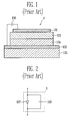
- FIG. 1 is a cross-sectional view showing a pixel of a conventional organic light emitting display. FIG. 2 is an equivalent circuit diagram of the pixel shown in FIG. 1.
- With reference to FIG. 1, the
pixel 1 includes ametal electrode 101, atransparent electrode 102, an organicphosphorous layer 103, and an organichole transport layer 104. Themetal electrode 101 functions as a cathode, and thetransparent electrode 102 functions as an anode. The organicphosphorous layer 103 and the organichole transport layer 104 are laminated between themetal electrode 101 and thetransparent electrode 102. The organicphosphorous layer 103 and the organichole transport layer 104 are made of organic compounds. - A
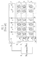
glass substrate 105 is located at an outer side of thetransparent electrode 102. A voltage from adrive source 106 is applied between themetal electrode 101 and thetransparent electrode 102. Energy is discharged by excitons generated by recombination of electrons and holes, which are respectively introduced from themetal electrode 101 and thetransparent electrode 102. Accordingly, thepixel 1 can emit light to the exterior through thetransparent electrode 102 and theglass substrate 105. Since thepixel 1 has a structure in which the organic phosphorous layer is laminated between the electrodes, an equivalent electric circuit diagram thereof has parasitic capacitances. In more detail, as shown in FIG. 2, thepixel 1 includes an illuminant (or a light emitting element) 107 and aparasitic capacitance 109, which are connected with each other in parallel. - FIG. 3 is a schematic view showing a conventional organic light emitting display. FIG. 4 is a timing diagram showing application of a drive current for driving the organic light emitting display shown in FIG. 3.
- With reference to FIG. 3 and FIG. 4, the conventional organic light emitting display includes an organic light
emitting display panel 2, a controller 21, a scan driver 6, and a data driver 5. - In the organic light
emitting display panel 2, column lines D1, D2,..., Dm and row lines S1, S2, ..., Sn cross each other at predetermined intervals.Pixels 1, namely, organic light emitting diodes, are formed at crossings of the column lines D1, D2,..., Dm and the row lines S1, S2, ..., Sn. - The controller 21 processes externally inputted image signals SIM, and provides data control signals SDA and scan control signals SSC to the data driver 5 and the scan driver 6, respectively. Here, the data control signals SDA include data signals, and the scan control signals SSC include switching control signals to generate a scan signal. The data driver 5 is electrically connected to the column lines D1, D2, ..., Dm. The data driver 5 generates and provides a drive current corresponding to the data signals from the controller 21 to the column lines D1, D2, ..., Dm according to the data control signals SDA from the controller 21.
- The scan driver 6 is electrically connected to the row lines S1, S2, ..., Sn. The scan driver 6 sequentially provides a scan signal to the row lines S1, S2, ..., Sn according to the switching control signals SSC from the controller 21.
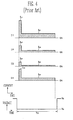
- As shown in FIG. 4, during a drive period Td of an organic light emitting diode in one pixel, a ground voltage switching element (see, for example, Mg1 in FIG. 3) is turned-on to apply a ground voltage to a row line. During time periods except for the drive period, a scan voltage switching element (see, for example, MS1 in FIG. 3) is turned-on to apply a scan voltage to the row line. As shown in FIG. 4, during the drive period Td, a drive current is applied to a column line corresponding to a pixel. That is, during a drive period Td of a first row line S1, drive currents I1, I2, ..., Im are respectively applied to the column lines D1, D2,..., Dm and flow through the
respective pixels 1. As shown in FIG. 4, because thepixel 1 is equivalently represented by the illuminant 107 and theparasitic capacitance 109 connected in parallel with each other (see, for example, FIG. 2), the drive currents I1, I2, ..., Im are divided into first drive currents Ic1, Ic2, ..., Icm and second drive currents Id1, Id2, ..., Idm. The first drive currents Ic1, Ic2, ..., Icm function to charge the respectiveparasitic capacitances 109, whereas the second drive currents Id1, Id2, ..., Idm are supplied to therespective illuminants 107 after a charge of the correspondingparasitic capacitances 109. FIG. 4 shows drive currents I1, I2, I3, and I4, which are respectively applied to a first column line D1, a second column line D2, a third column line D3, and a fourth column line D4. -
Japanese patent publication No. 1999-231834 - However, in
Japanese patent publication No. 1999-231834 - Accordingly, aspects of the present invention respectively provide an organic light emitting display and a driving method thereof capable of reducing manufacturing cost of a driver that applies a drive current to an organic light emitting diode of a pixel via a column line.
- According to a first aspect of the invention, there is provided an organic light emitting display as set out in
claim 1. Preferred features of this aspect are set out inclaims 2 to 11. - According to a second aspect of the present invention, there is provided a method for driving an organic light emitting display as set out in
claim 12. Preferred features of this aspect are set out inclaims 13 to 20. - These and/or other aspects and features of the invention will become apparent and more readily appreciated from the following description of embodiments of the present invention, taken in conjunction with the accompanying drawings of which:
- FIG. 1 is a cross-sectional view showing a pixel of a conventional organic light emitting display;
- FIG. 2 is an equivalent circuit diagram of the pixel shown in FIG. 1;
- FIG. 3 is a schematic view showing a conventional organic light emitting display;
- FIG. 4 is a timing diagram showing application of a drive current for driving the organic light emitting display shown in FIG. 3;
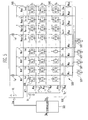
- FIG. 5 is a schematic diagram showing an organic light emitting display according to an embodiment of the present invention; and
- FIG. 6 is a timing diagram showing drive currents applied via column lines of FIG. 5 and an operation of a charge switch.
- Hereinafter, embodiments according to the present invention will be described with reference to the accompanying drawings. Here, when a first element is described as being connected to a second element, the first element may not only be directly connected to the second element but may alternately be indirectly connected to the second element via a third element. Further, elements that are not essential to the complete understanding of the invention are not shown to improve clarity. Also, like reference numerals refer to like elements throughout.
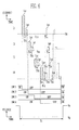
- FIG. 5 is a schematic diagram showing an organic light emitting display according to an embodiment of the present invention. FIG. 6 is a timing diagram showing drive currents applied via column lines of FIG. 5 and an operation of a charge switch.
- Referring to FIG. 5, the organic light emitting display in one embodiment includes an organic light
emitting display panel 502, acontroller 521, ascan driver 506, adata driver 505, acharge switch 508, andvoltage retaining circuits 507. - The organic light
emitting display panel 502 includes column lines D1, D2,..., Dm, row lines S1, S2, ..., Sn, andpixels 1. The column lines D1, D2,..., Dm and the row lines S1, S2, ..., Sn cross each other at certain intervals which may be predetermined. As shown in FIG. 5, organic light emitting diodes of thepixels 1 are formed at crossings of the column lines D1, D2,..., Dm and the row lines S1, S2, ..., Sn. - Each of the
pixels 1 includes a metal electrode, a transparent electrode, an organic phosphorous layer, and an organic hole transport layer. The metal electrode functions as a cathode, and the transparent electrode functions as an anode. The organic phosphorous layer and the organic hole transport layer are laminated between the metal electrode and the transparent electrode. The organic phosphorous layer and the organic hole transport layer are made of organic compounds. - When a voltage is applied between the metal electrode and the transparent electrode, excitons are generated due to recombination between electrons and holes, which are respectively introduced from the metal electrode and the transparent electrode. When the excitons transition from an excited state to a ground state, light is emitted. The emitted light is discharged through the transparent electrode and a glass substrate.
- Here, since the
pixel 1 includes a structure in which the organic phosphorous layer is laminated between the electrodes, an equivalent electric circuit thereof has parasitic capacitances. Accordingly, thepixel 1 can be considered to include an illuminant (or a light emitting element) 107 and aparasitic capacitance 109, which are connected with each other in parallel. - The
controller 521 processes externally inputted image signals SIM, and provides data control signals SDA and scan control signals SSC to thedata driver 505 and thescan driver 506, respectively. Here, the data control signals SDA include data signals, and the scan control signals SSC include switching control signals to generate a scan signal. - The
data driver 505 is electrically connected to the column lines D1, D2, ..., Dm. Thedata driver 505 generates and provides a drive current corresponding to the data signals from thecontroller 521 to the column lines D1, D2, ..., Dm according to the data control signals SDA from thecontroller 521. - In a conventional organic light emitting display, drive currents output from current sources I1, I2, ..., Im in the data driver 5 (see, for example, FIG. 3) are provided to respective column lines D1, D2, ..., Dm. However, in embodiments of the present invention, in order to reduce manufacturing cost of a data driver, the column lines D1, D2, ..., Dm are grouped as a plurality of groups, e.g., k groups. That is, each of the column lines belong to one of the groups. A drive current from one common current source is supplied to the column lines in one group.
- Here, the
data driver 505 according to this embodiment of the present invention performs a switching operation such that drive currents from one of common current sources Ig1, Ig2, .., Igk are applied to the respective group of column lines in a time-division manner. Thedata driver 505 includes drive switching elements, which are connected between the common current sources and the respective column lines. - In the embodiment shown in FIG. 5, first column line D1, second column line D2, third column line D3, and fourth column line D4 form one group. A first switching element Mdl, a second switching element Md2, a third switching element Md3, and a fourth switching element Md4 are connected between a first common current source Ig1 and the first column line D1, the second column line D2, the third column line D3, and the fourth column line D4, respectively, such that a drive current from the first common current source Ig1 can be applied to the group in a time-division manner.
- That is, FIG. 5 shows an organic light emitting display wherein m column lines are divided into k groups by forming 4 column lines connected to a unit pixel as one group. In one embodiment, a red (R) emission pixel, a green (G) emission pixel, a blue (B) emission pixel, and a white (W) emission pixel form the unit pixel.
- However, embodiments of the present invention are not limited thereto. That is, the number of column lines that form one group can vary.
- By way of example, when a red (R) emission pixel, a green (G) emission pixel, and a blue (B) emission pixel form the unit pixel, 3 column lines are grouped as one group. In one embodiment, a drive current from a common current source is applied to a red (R) pixel on which a red (R) phosphorous layer is laminated, a green (G) pixel on which a green (G) phosphorous layer is laminated, and a blue (B) pixel on which a blue (B) phosphorous layer is laminated in a time-division manner.
- In one embodiment, since a plurality of column lines are connected to one common current source, a drive current from the common current source is sequentially applied to the plurality of column lines. Here, while the drive current is applied to one column line, the drive current is not applied to other column lines. This will be described in more detail with reference to FIG. 6 later.
- The
scan driver 506 is electrically connected to row lines S1, S2, ..., Sn. Thescan driver 506 sequentially provides a scan signal to therow lines S 1, S2, ..., Sn according to switching control signals from thecontroller 521. The scan signal has a high level Vs and a low level Vg. The scan signal maintains the high level Vs by default. During a drive period Td of driving a row line, however, the scan signal becomes the low level Vg. - Here, the
scan driver 506 includes a first scan voltage source Vs, first scan switching elements Ms1, Ms2, ..., Msn, a second scan voltage source Vg, and second scan switching elements Mg1, Mg2, ..., Mgn. The first scan voltage source Vs provides a signal of a high level Vs. The first scan switching elements Ms1, Ms2, ..., Msn are electrically connected to the first scan voltage source Vs, and transfer the signal of a high level Vs to the row lines S1, S2, ..., Sn. The second scan voltage source Vg provides a voltage of a low level Vg. The second scan switching elements Mg1, Mg2, ..., Mgn are electrically connected to the second scan voltage source Vg, and transfer the voltage of a low level Vg to the row lines S1, S2, ..., Sn. - That is, the first scan switching elements Ms1, Ms2, ..., Msn are turned-on and the second scan switching elements Mg1, Mg2, ..., Mgn are turned-off to provide the signal of a high level Vs to the row lines S1, S2, ..., Sn. In contrast to this, during the drive period Td, the first scan switching elements Ms1, Ms2, ..., Msn are turned-off and the second scan switching elements Mg1, Mg2, ..., Mgn are turned-on to provide the signal of a low level Vg to the row lines S1, S2, ..., Sn.
- In one embodiment, the first scan voltage source Vs of a high level has a level similar to that of a drive
voltage source V 1 in a data driver (see, for example, thedata driver 505 in FIG. 5), and the first scan switching elements Ms1, Ms2, ..., Msn are turned-on to apply the voltage of a high level Vs to the row lines S1, S2, ..., Sn. Accordingly, because there is substantially no potential difference between an anode and a cathode of each diode connected thereto, each diode does not emit light. In contrast, during a drive period of each pixel, a scan voltage provided to a row line corresponds to a second scan voltage source Vg of a low level. - Here, as shown in FIG. 5, the low level Vg may be a voltage ground GND. Hereinafter, a ground voltage may be referred to as 'low level'.
- During the drive period Td, a ground voltage Vg, GND is applied to the row line, and a drive current is applied to a column line, such that the drive current flows to a ground terminal through a pixel, with the result that the pixel emits light.
- In addition, referring to FIG. 5, in an embodiment of the present invention, respective column lines are connected to
voltage retaining circuits 507 through acharge switch 508. - Here, each of the
voltage retaining circuits 507 corresponds to column lines, which are connected to pixels that emit light of the same color. - In more detail, as shown in FIG. 5, four
voltage retaining circuits 507 are provided corresponding to groups of column lines, which are connected to pixels that emit light of red (R), green (G), blue (B), and white (W) colors, respectively. Acharge switch 508 connected to the respective column lines is coupled with thevoltage retaining circuits 507, which are installed (or positioned) corresponding to respective colors. - The
voltage retaining circuit 507 functions to generate a bias voltage, and includes a Zener diode and a parallel capacitor. However, it is not essential that the parallel capacitor be included therein. - In one embodiment, the
voltage retaining circuit 507 is constructed by a voltage regulation source, which generates a voltage which may be predetermined. In one embodiment, the voltage is a voltage corresponding to a black level of the organic light emitting display. - In one embodiment, an anode of a Zener diode can be connected to the column lines, and a cathode thereof is connected to ground. Charge switches 508 connect the
voltage retaining circuits 507 and the column lines. The charge switches 508 turn-on/off connections of the column lines and thevoltage retaining circuits 507. Here, a potential of the Zener diode is high such that it is possible to determine a black level of each color. - That is, when the
charge switch 508 connected to respectivevoltage retaining circuits 507 positioned according to colors is turned-on, the respectivevoltage retaining circuits 507 couple column lines connected to pixels that emit light of the same color with each other. As a result, the column lines are coupled with an anode side of the Zener diode of a correspondingvoltage retaining circuit 507. - However, before a drive current is applied to the column line, the
corresponding charge switch 508 is turned-on. Turing-on of thecharge switch 508 reduces a charge current supplied to an organic light emitting diode, which is connected to a row line not selected when row lines are switched. - Accordingly, a charge flows from an organic light emitting diode which was driven and emitted light, such that other coupled organic light emitting diodes are charged. Voltages at anode sides of the other organic light emitting diodes are determined by the voltage retaining circuits and maintain a potential VH, which may be predetermined. The potential VH is a voltage at which an organic light emitting diode reaches a black level. The organic light emitting diode includes a cathode, which is connected to ground. Accordingly, pixels connected to the data lines and that emit light of the same color are preliminarily charged to become a black level.
- Hereinafter, a method for driving an organic light emitting display according to an embodiment of the present invention will be described in more detail referring to FIG. 6.
- Each of a plurality of column lines belong to one of a plurality of groups. A drive current from a common current source is applied to the column lines in one group. Here, the drive current is sequentially applied to column line by column line such that application of the drive current to the individual column lines do not overlap with each other over time. Concurrently, the corresponding charge switch is turned-on prior to applying the drive current to preliminarily charge pixels coupled with column lines in the one group.
- In addition, the drive currents I1, I2, ..., Im are divided into first drive currents Ic1, Ic2, ..., Icm for charging a parasitic capacitance of a pixel and second drive currents Id1, Id2, ..., Idm which are supplied to an illuminant of the pixel. To sequentially apply the drive currents to column lines of the same group, embodiments of the present invention use a method of intermittently applying the drive current thereto.
- That is, in embodiments of the present invention, the pixels are preliminarily charged and the first drive current is provided through the charge switch and the voltage retaining circuit, thereby quickly charging a parasitic capacitance of each pixel.
- As shown in FIG. 6, when first to fourth column lines D1 to D4 are grouped as a first group G1, a first drive current Ic1 is applied during a time period T11 and a second drive current Id1 is applied during a time period T12. No currents are applied to the second to fourth column lines D2 to D4 during the time periods T11 and T12.
- Next, a first drive current Ic2 is applied to the second column line D2 during a time period T21, and a second drive current Id2 is applied to the second column line D2 during a time period T22. No currents are applied to the first, third and fourth column lines D1, D3 and D4 during the time periods T21 and T22.
- Next, a first drive current Ic3 is applied to the third column line D3 during a time period T31, and a second drive current Id3 is applied to the third column line D3 during a time period T32. No currents are applied to the first, second and fourth column lines D1, D2 and D4 during the time periods T31 and T32.
- Thereafter, a first drive current Ic4 is applied to the fourth column line D4 during a time period T41, and a second drive current Id4 is applied to the fourth column line D4 during a time period T42. No currents are applied to the first to third column lines D1 to D3 during the time periods T41 and T42.
- The application of the drive current, as described above, is performed by turning-on/off operation of the first to fourth drive switching elements Md1 to Md4, which are connected to the first common current source Ig1.
- In some embodiments, the drive currents I1 to I4 are respectively applied to the first to fourth
column lines D 1 to D4, as described above, to cause each pixel to emit light. In other embodiments (such as the one shown in Figure 6), drive current, that is, second drive currents Id1 to Id4 is further applied to each pixel. - In more detail, after the time period T42, a second drive current Id1 is applied to the first column line D1 during a time period T14. No currents are applied to the second to fourth column lines D2 to D4 during the
time period T 14. - After the time period T14, a second drive current Id2 is applied to the second column line D2 during a time period T24. No currents are applied to the first, third, and fourth column lines D1, D3, and D4 during the time period T24.
- After the time period T24, a second drive current Id3 is applied to the third column line D3 during a time period T34. No currents are applied to the first, second and fourth column lines D1, D2 and D4 during the time period T34.
- After the time period T34, a second drive current Id2 is again applied to the fourth column D4 during a time period T44. No currents are applied to the first to third column lines D1 to D3 during the time period T44. In some embodiments, e.g., when the drive currents I1 to I4 applied to each pixel are insufficient, time periods such as the time periods T14 to T44 can be repeated according to any of various suitable cycles.
- In this embodiment, the first to fourth column lines D1 to D4 are grouped as a first group G1. A first charge switch SW11 (see, for example, FIG. 5) connected to the first column line D1 is turned-on before a drive current is applied to the first column line D1. In contrast to this, during most of the drive period Td of FIG. 6, the first charge switch SW11 is turned-off. In addition, a second charge switch SW12 connected to the second column line D2 is turned-on before a drive current is applied to the second column line D2. In contrast to this, during most of a remaining portion of the drive period, the second charge switch SW12 is turned-off.
- In a substantially similar manner, a third charge switch SW13 connected to the third column line D3 is turned-on before the drive current is applied to the third column line D3. In contrast to this, during most of a remaining portion of the drive period, the third
charge switch SW 13 is turned-off. In addition, a fourth charge switch SW14 connected to the fourth column line D4 is turned-on before the drive current is applied to the fourth column line D4. In contrast to this, during most of a remaining portion of the drive period, the fourth charge switch SW14 is turned-off. - As described above, respective pixels connected to the column lines are preliminarily charged through a respective
voltage retaining circuit 507 by a turning-on/off operation of the charge switches 508. - In this embodiment, during the drive period Td, the first drive currents Ic1, Ic2, ..., Icm are respectively applied to the
column lines D 1, D2, ..., Dm during the first periods T11, ..., Tm1, the second drive currents Id1, Id2, ..., Idm are respectively applied thereto during the second periods T12, ..., Tm2, and no currents are applied to a corresponding one of the column lines D1, D2, ..., Dm during third periods T13, ..., Tm3. The second drive currents Id1, Id2, ..., Idm are again applied thereto during the fourth periods T14, ..., Tm4. The third periods T13, ..., Tm3 and the fourth periods T14, ..., Tm4 are repeated until the drive period Td is terminated. - In embodiments of the present invention, after the first drive current is applied to one column line during the drive period Td, the second drive current is intermittently applied. The drive method according to embodiments of the present invention, as described above, is different from a conventional drive method, but they do not substantially differ from each other with respect to light emission of a pixel.
- In some embodiments, the second drive currents Id1, Id2, ..., Idm are respectively applied to the column lines D1, D2, ..., Dm before the first periods T11, ..., Tm1 during the drive period Td. That is, when the second drive currents Id1, Id2, ..., Idm are applied ahead of the first drive currents Ic1, Ic2, ..., Icm, and the first drive currents Ic1, Ic2, ..., Icm are gradually increased, a loss of a circuit device in the driving circuit may be prevented.
- In the driving method according to embodiments of the present invention, a plurality of column lines belong to one group, and a drive current from a common current source is sequentially applied to the one group in such a way that the drive current is intermittently applied to one column line. However, embodiments of the present invention are not limited thereto. For example, respective drive currents from respective current sources can be intermittently applied to respective column lines.
- In more detail, in the organic light emitting display having a connection construction of column lines, as shown in FIG. 3, and a current source, a drive current I1 applied to a first column line of FIG. 6 may be intermittently applied to each pixel.
- As described above, embodiments of the present invention may have certain features as follows.
- In embodiments of the organic light emitting display, since the number of current sources providing a drive current applied to respective column lines is reduced, manufacturing cost of a data driver is reduced, and accordingly the total manufacturing cost of the organic light emitting display can be lowered.
- In addition, although a drive current is intermittently applied to respective pixels, the respective pixels can emit light according to the applied drive current, thereby preventing a performance of emission characteristics thereof from being deteriorated.
- Although a few embodiments of the present invention have been shown and described, it would be appreciated by those skilled in the art that changes might be made in these embodiments without departing from the principles of the invention, the scope of which is defined in the claims and their equivalents.
Claims (20)
- An organic light emitting display comprising:a plurality of column lines adapted to receive a drive current, each of the column lines belonging to one of a plurality of groups;a plurality of row lines adapted to receive a scan signal;a plurality of organic light emitting diodes of a plurality of pixels, which are located at crossings of the row lines and the column lines;a scan driver for applying the scan signal to the row lines;a data driver including a common current source and a plurality of drive switching elements, the common current source being adapted to apply the drive current to the column lines in one of the groups, and the drive switching elements being electrically connected to the common current source and being adapted to apply the drive current to the column lines in said one of the groups within a drive period in which the scan signal is applied;a plurality of charge switches electrically connected to the column lines, the charge switches being adapted to be turned-on before the drive current is applied to the column lines, and being adapted to be turned-off during the drive period; anda voltage retaining circuit coupled with the charge switches, for preliminarily charging the pixels.
- An organic light emitting display according to claim 1, wherein the voltage retaining circuit includes four circuits, each circuit corresponding to a respective column line, each column line being connected to pixels for emitting light of a respective one of red (R), green (G), blue (B), and white (W) color.
- An organic light emitting display according to claim 1, wherein the voltage retaining circuit includes three circuits, each circuit corresponding to a respective column line, each column line being connected to pixels for emitting lights of a respective one of red (R), green (G), and blue (B) color.
- An organic light emitting display according to any one of claims 1 to 3, wherein the voltage retaining circuit includes a voltage regulation element for maintaining a voltage and a capacitor electrically connected with the voltage regulation element in parallel.
- An organic light emitting display according to claim 4, wherein the voltage maintained by the voltage regulation element is a voltage corresponding to a black level of the organic light emitting display.
- An organic light emitting display according to claim 4 or 5,
wherein the voltage regulation element comprises a Zener diode. - An organic light emitting display according to any one of claims 1 to 6, wherein the voltage retaining circuit comprises a voltage regulation source.
- An organic light emitting display according to any one of claims 1 to 7,
wherein the drive current comprises a first drive current and a second drive current,
wherein the drive period comprises a first period, a second period, a third period, and a fourth period,
wherein the first drive current is applied to one of the column lines during the first period,
wherein the second drive current is applied to the one of the column lines during the second period and has a lower amplitude than an amplitude of the first drive current,
wherein the drive current is not applied to the one of the column lines during the third period, and
wherein the second drive current is applied to the one of the column lines during the fourth period. - An organic light emitting display according to claim 8, wherein the drive period further comprises a time period in which the drive current is not applied to the one of the column lines and a time period in which the second drive current is applied to the one of the column lines, after the fourth period.
- An organic light emitting display according to any one of claims 1 to 9, wherein the scan driver comprises:a first scan voltage source for supplying a signal of a high level;a first scan switching element electrically connected to the first scan voltage source and adapted to be turned-on to apply the signal of a high level to the row lines;a second scan voltage source for supplying a signal of a low level; anda second scan switching element electrically connected to the second scan voltage source and adapted to be turned-on to apply the signal of a low level to the row lines,wherein the first scan switching element is turned-off and the second scan switching element is turned-on during the drive period.
- An organic light emitting display according to any one of claims 1 to 10, wherein, while the drive current is applied to one of the column lines in said one of the groups, the drive current is not applied to other of the column lines in said one of the groups.
- A method for driving an organic light emitting display including a plurality of column lines adapted to receive a drive current, each of the column lines belonging to one of a plurality of groups, a plurality of row lines adapted to receive a scan signal, and an organic light emitting diode in at least one pixel, which is located at a crossing of one of the row lines and one of the column lines, the at least one pixel being adapted to receive the drive current and to emit light, the method comprising the steps of:applying the drive current from a common current source to the column lines in one of the groups in a time-division manner during a drive period; andpreliminarily charging the at least one pixel before the drive current is applied to the column lines in said one of the groups.
- A method according to claim 12, wherein the drive current is intermittently applied to the column lines in said one of the groups during the drive period.
- A method according to claim 12 or 13,
wherein the drive current comprises a first drive current and a second drive current;
wherein the drive period comprises a first period, a second period, a third period, and a fourth period,
wherein the first drive current is applied to one of the column lines during the first period,
wherein the second drive current is applied to the one of the column lines during the second period, the second drive current having a lower amplitude than an amplitude of the first drive current,
wherein the drive current is not applied to the one of the column lines during the third period, and
wherein the second drive current is applied to the one of the column lines during the fourth period. - A method according to claim 14, wherein the drive period further comprises a time period in which the drive current is not applied to the one of the column lines and a time period in which the second drive current is applied to the one of the column lines, after the fourth period.
- A method according to claim 14 or 15, wherein the second drive current is applied to the one of the column lines before the first period.
- A method according to any one of claims 14 to 16, wherein the respective amplitudes of the first and second drive currents vary among the at least one pixel.
- A method according to any one of claims 12 to 17, wherein, while the drive current is applied to one of the column lines in said one of the groups, the drive current is not applied to other of the column lines in said one of the groups.
- A method according to any one of claims 12 to 18, wherein each column line in said one of the groups is connected to the pixels for emitting lights of a respective one of red (R), green (G), blue (B), and white (W) colors.
- A method according to any one of claims 12 to 18, wherein each column lines in said one of the groups is connected to the pixels for emitting lights of a respective one of red (R), green (G), and blue (B) colors.
Applications Claiming Priority (1)
| Application Number | Priority Date | Filing Date | Title |
|---|---|---|---|
| KR1020060063940A KR100852349B1 (en) | 2006-07-07 | 2006-07-07 | Organic light emitting display device and driving method thereof |
Publications (2)
| Publication Number | Publication Date |
|---|---|
| EP1876582A2 true EP1876582A2 (en) | 2008-01-09 |
| EP1876582A3 EP1876582A3 (en) | 2009-09-16 |
Family
ID=38529400
Family Applications (1)
| Application Number | Title | Priority Date | Filing Date |
|---|---|---|---|
| EP07251686A Withdrawn EP1876582A3 (en) | 2006-07-07 | 2007-04-23 | Organic light emitting display and driving method thereof |
Country Status (5)
| Country | Link |
|---|---|
| US (1) | US7999771B2 (en) |
| EP (1) | EP1876582A3 (en) |
| JP (1) | JP4829093B2 (en) |
| KR (1) | KR100852349B1 (en) |
| CN (1) | CN101101730B (en) |
Cited By (2)
| Publication number | Priority date | Publication date | Assignee | Title |
|---|---|---|---|---|
| EP3220379A1 (en) * | 2016-03-17 | 2017-09-20 | Leyard Optoelectronic Co., Ltd | Display circuit and control method therefor |
| WO2018088668A1 (en) | 2016-11-09 | 2018-05-17 | Samsung Electronics Co., Ltd. | Led display module and display apparatus |
Families Citing this family (8)
| Publication number | Priority date | Publication date | Assignee | Title |
|---|---|---|---|---|
| KR101056241B1 (en) * | 2008-12-19 | 2011-08-11 | 삼성모바일디스플레이주식회사 | Organic light emitting display |
| CN102347003B (en) * | 2010-08-05 | 2014-08-20 | 国琏电子(上海)有限公司 | Light source brilliance control apparatus |
| KR102054849B1 (en) * | 2013-06-03 | 2019-12-12 | 삼성디스플레이 주식회사 | Organic Light Emitting Display Panel |
| CN105702213B (en) * | 2016-03-22 | 2018-07-06 | 北京大学深圳研究生院 | Display device and its display driver |
| CN107221286B (en) * | 2017-07-27 | 2019-04-05 | 芯颖科技有限公司 | Drive circuit, drive current control method and processor |
| TWI739099B (en) * | 2019-05-01 | 2021-09-11 | 友達光電股份有限公司 | Display module, displayer, and the driving method thereof |
| WO2022097767A1 (en) * | 2020-11-04 | 2022-05-12 | 엘지전자 주식회사 | Display device using semiconductor light-emitting element and method for controlling same |
| CN113205776B (en) * | 2021-04-28 | 2022-08-30 | 北京大学深圳研究生院 | Data line driving unit, display system and gray scale related remote auxiliary driving method |
Citations (3)
| Publication number | Priority date | Publication date | Assignee | Title |
|---|---|---|---|---|
| JPH11231834A (en) | 1998-02-13 | 1999-08-27 | Pioneer Electron Corp | Luminescent display device and its driving method |
| US20020101179A1 (en) | 2000-12-28 | 2002-08-01 | Shingo Kawashima | Organic electroluminescence driving circuit, passive matrix organic electroluminescence display device, and organic electroluminescence driving method |
| US20060071884A1 (en) | 2004-09-22 | 2006-04-06 | Kim Yang W | Organic light emitting display |
Family Cites Families (19)
| Publication number | Priority date | Publication date | Assignee | Title |
|---|---|---|---|---|
| JP3568097B2 (en) | 1998-04-22 | 2004-09-22 | パイオニア株式会社 | Light emitting display and driving method thereof |
| JP2002108284A (en) | 2000-09-28 | 2002-04-10 | Nec Corp | Organic el display device and its drive method |
| US6323631B1 (en) | 2001-01-18 | 2001-11-27 | Sunplus Technology Co., Ltd. | Constant current driver with auto-clamped pre-charge function |
| JP3951687B2 (en) * | 2001-08-02 | 2007-08-01 | セイコーエプソン株式会社 | Driving data lines used to control unit circuits |
| JP2003167556A (en) * | 2001-11-29 | 2003-06-13 | Hitachi Ltd | Matrix type display device, drive control device and drive control method thereof |
| JP3982249B2 (en) * | 2001-12-11 | 2007-09-26 | 株式会社日立製作所 | Display device |
| JP4029840B2 (en) | 2002-01-17 | 2008-01-09 | 日本電気株式会社 | Semiconductor device having matrix type current load driving circuit and driving method thereof |
| JP2003255903A (en) * | 2002-02-28 | 2003-09-10 | Toshiba Corp | Display device |
| KR100432554B1 (en) | 2002-11-29 | 2004-05-24 | 하나 마이크론(주) | organic light emitting device display driving apparatus and the method thereof |
| JP2004191752A (en) * | 2002-12-12 | 2004-07-08 | Seiko Epson Corp | Electro-optical device, electro-optical device driving method, and electronic apparatus |
| KR20050034113A (en) * | 2003-10-08 | 2005-04-14 | 삼성전자주식회사 | Organic electro luminescence display |
| KR100599724B1 (en) | 2003-11-20 | 2006-07-12 | 삼성에스디아이 주식회사 | Display panel, light emitting display device using same and driving method thereof |
| JP4640755B2 (en) | 2004-01-19 | 2011-03-02 | 東北パイオニア株式会社 | Driving device and driving method of light emitting display panel |
| KR101126343B1 (en) * | 2004-04-30 | 2012-03-23 | 엘지디스플레이 주식회사 | Electro-Luminescence Display Apparatus |
| KR100581800B1 (en) * | 2004-06-07 | 2006-05-23 | 삼성에스디아이 주식회사 | Organic electroluminescent display and demultiplexer |
| JP2006003752A (en) | 2004-06-18 | 2006-01-05 | Casio Comput Co Ltd | Display device and drive control method thereof |
| KR100581810B1 (en) * | 2004-08-25 | 2006-05-23 | 삼성에스디아이 주식회사 | Light emitting display device and driving method thereof |
| JP2006126232A (en) * | 2004-10-26 | 2006-05-18 | Seiko Epson Corp | Electro-optical device, electronic apparatus, and driving method of electro-optical device |
| KR100604060B1 (en) * | 2004-12-08 | 2006-07-24 | 삼성에스디아이 주식회사 | Light emitting display device and driving method thereof |
-
2006
- 2006-07-07 KR KR1020060063940A patent/KR100852349B1/en active Active
- 2006-12-20 JP JP2006343292A patent/JP4829093B2/en active Active
-
2007
- 2007-03-29 US US11/693,603 patent/US7999771B2/en active Active
- 2007-04-23 EP EP07251686A patent/EP1876582A3/en not_active Withdrawn
- 2007-07-06 CN CN2007101283385A patent/CN101101730B/en active Active
Patent Citations (3)
| Publication number | Priority date | Publication date | Assignee | Title |
|---|---|---|---|---|
| JPH11231834A (en) | 1998-02-13 | 1999-08-27 | Pioneer Electron Corp | Luminescent display device and its driving method |
| US20020101179A1 (en) | 2000-12-28 | 2002-08-01 | Shingo Kawashima | Organic electroluminescence driving circuit, passive matrix organic electroluminescence display device, and organic electroluminescence driving method |
| US20060071884A1 (en) | 2004-09-22 | 2006-04-06 | Kim Yang W | Organic light emitting display |
Cited By (5)
| Publication number | Priority date | Publication date | Assignee | Title |
|---|---|---|---|---|
| EP3220379A1 (en) * | 2016-03-17 | 2017-09-20 | Leyard Optoelectronic Co., Ltd | Display circuit and control method therefor |
| US9900476B2 (en) | 2016-03-17 | 2018-02-20 | Leyard Optoelectronic Co., Ltd. | Display circuit and control method therefor |
| WO2018088668A1 (en) | 2016-11-09 | 2018-05-17 | Samsung Electronics Co., Ltd. | Led display module and display apparatus |
| EP3494572A4 (en) * | 2016-11-09 | 2019-06-12 | Samsung Electronics Co., Ltd. | LED DISPLAY MODULE AND DISPLAY APPARATUS |
| US10424240B2 (en) | 2016-11-09 | 2019-09-24 | Samsung Electronics Co., Ltd. | LED display module and display apparatus |
Also Published As
| Publication number | Publication date |
|---|---|
| JP2008015459A (en) | 2008-01-24 |
| KR20080004960A (en) | 2008-01-10 |
| US7999771B2 (en) | 2011-08-16 |
| JP4829093B2 (en) | 2011-11-30 |
| CN101101730B (en) | 2010-08-11 |
| KR100852349B1 (en) | 2008-08-18 |
| CN101101730A (en) | 2008-01-09 |
| EP1876582A3 (en) | 2009-09-16 |
| US20080007495A1 (en) | 2008-01-10 |
Similar Documents
| Publication | Publication Date | Title |
|---|---|---|
| US7999771B2 (en) | Organic light emitting display and driving method thereof | |
| KR100432173B1 (en) | Organic EL display device and method for driving the same | |
| KR101871188B1 (en) | Organic Light Emitting Display and Driving Method Thereof | |
| US7903052B2 (en) | Pixel driving circuit for a display device and a driving method thereof | |
| US6894436B2 (en) | Drive method of light-emitting display panel and organic EL display device | |
| KR101875127B1 (en) | Organic Light Emitting Display Device | |
| JP5382985B2 (en) | Organic electroluminescent display device and driving method thereof | |
| US6707438B1 (en) | Apparatus and method for driving multi-color light emitting display panel | |
| JP4641896B2 (en) | Light emitting display device, demultiplexing circuit and driving method thereof | |
| US6486607B1 (en) | Circuit and system for driving organic thin-film EL elements | |
| JPH11231834A (en) | Luminescent display device and its driving method | |
| US6333738B1 (en) | Display panel driving apparatus of a simplified structure | |
| US7944419B2 (en) | Flat panel display having pre-charging circuit | |
| US6922180B2 (en) | Driving apparatus of display panel | |
| US8379008B2 (en) | Organic light emitting display device and power supply unit for the same | |
| US20030107536A1 (en) | Light emitting circuit for organic electroluminescence element and display device | |
| US6894685B2 (en) | Driving method for luminous elements | |
| US6882330B2 (en) | Field emission displaying device and driving method thereof | |
| KR100581809B1 (en) | Demultiplexing circuit and light emitting display device using the same | |
| JP3646916B2 (en) | Multicolor light emitting display panel drive device | |
| KR100829745B1 (en) | A method of driving an organic light emitting display device and an organic light emitting display device driven thereby | |
| JP2003140610A (en) | Organic electroluminescence panel and method for driving the same | |
| US7119763B2 (en) | Light emitting circuit for organic electroluminescence element and display device | |
| KR101066355B1 (en) | Driving circuit and driving method thereof of passive matrix organic electroluminescent display | |
| JP4033002B2 (en) | Display device and display panel driving method |
Legal Events
| Date | Code | Title | Description |
|---|---|---|---|
| PUAI | Public reference made under article 153(3) epc to a published international application that has entered the european phase |
Free format text: ORIGINAL CODE: 0009012 |
|
| 17P | Request for examination filed |
Effective date: 20070427 |
|
| AK | Designated contracting states |
Kind code of ref document: A2 Designated state(s): AT BE BG CH CY CZ DE DK EE ES FI FR GB GR HU IE IS IT LI LT LU LV MC MT NL PL PT RO SE SI SK TR |
|
| AX | Request for extension of the european patent |
Extension state: AL BA HR MK YU |
|
| RAP1 | Party data changed (applicant data changed or rights of an application transferred) |
Owner name: SAMSUNG MOBILE DISPLAY CO., LTD. |
|
| PUAL | Search report despatched |
Free format text: ORIGINAL CODE: 0009013 |
|
| AK | Designated contracting states |
Kind code of ref document: A3 Designated state(s): AT BE BG CH CY CZ DE DK EE ES FI FR GB GR HU IE IS IT LI LT LU LV MC MT NL PL PT RO SE SI SK TR |
|
| AX | Request for extension of the european patent |
Extension state: AL BA HR MK RS |
|
| AKX | Designation fees paid |
Designated state(s): DE FR GB HU PL |
|
| 17Q | First examination report despatched |
Effective date: 20110518 |
|
| STAA | Information on the status of an ep patent application or granted ep patent |
Free format text: STATUS: THE APPLICATION IS DEEMED TO BE WITHDRAWN |
|
| 18D | Application deemed to be withdrawn |
Effective date: 20110929 |