EP1872477B1 - System und verfahren zum mischen logischer daten auf drei ebenen zur überabtastungsdatenkonvertierung - Google Patents
System und verfahren zum mischen logischer daten auf drei ebenen zur überabtastungsdatenkonvertierung Download PDFInfo
- Publication number
- EP1872477B1 EP1872477B1 EP06749962A EP06749962A EP1872477B1 EP 1872477 B1 EP1872477 B1 EP 1872477B1 EP 06749962 A EP06749962 A EP 06749962A EP 06749962 A EP06749962 A EP 06749962A EP 1872477 B1 EP1872477 B1 EP 1872477B1
- Authority
- EP
- European Patent Office
- Prior art keywords
- data
- neg
- pos
- shuffler
- thermometer
- Prior art date
- Legal status (The legal status is an assumption and is not a legal conclusion. Google has not performed a legal analysis and makes no representation as to the accuracy of the status listed.)
- Not-in-force
Links
Images


Classifications
-
- H—ELECTRICITY
- H03—ELECTRONIC CIRCUITRY
- H03M—CODING; DECODING; CODE CONVERSION IN GENERAL
- H03M1/00—Analogue/digital conversion; Digital/analogue conversion
- H03M1/06—Continuously compensating for, or preventing, undesired influence of physical parameters
- H03M1/0617—Continuously compensating for, or preventing, undesired influence of physical parameters characterised by the use of methods or means not specific to a particular type of detrimental influence
- H03M1/0634—Continuously compensating for, or preventing, undesired influence of physical parameters characterised by the use of methods or means not specific to a particular type of detrimental influence by averaging out the errors, e.g. using sliding scale
- H03M1/0656—Continuously compensating for, or preventing, undesired influence of physical parameters characterised by the use of methods or means not specific to a particular type of detrimental influence by averaging out the errors, e.g. using sliding scale in the time domain, e.g. using intended jitter as a dither signal
- H03M1/066—Continuously compensating for, or preventing, undesired influence of physical parameters characterised by the use of methods or means not specific to a particular type of detrimental influence by averaging out the errors, e.g. using sliding scale in the time domain, e.g. using intended jitter as a dither signal by continuously permuting the elements used, i.e. dynamic element matching
- H03M1/067—Continuously compensating for, or preventing, undesired influence of physical parameters characterised by the use of methods or means not specific to a particular type of detrimental influence by averaging out the errors, e.g. using sliding scale in the time domain, e.g. using intended jitter as a dither signal by continuously permuting the elements used, i.e. dynamic element matching using different permutation circuits for different parts of the digital signal
-
- H—ELECTRICITY
- H03—ELECTRONIC CIRCUITRY
- H03M—CODING; DECODING; CODE CONVERSION IN GENERAL
- H03M1/00—Analogue/digital conversion; Digital/analogue conversion
- H03M1/06—Continuously compensating for, or preventing, undesired influence of physical parameters
- H03M1/0617—Continuously compensating for, or preventing, undesired influence of physical parameters characterised by the use of methods or means not specific to a particular type of detrimental influence
- H03M1/0675—Continuously compensating for, or preventing, undesired influence of physical parameters characterised by the use of methods or means not specific to a particular type of detrimental influence using redundancy
- H03M1/0678—Continuously compensating for, or preventing, undesired influence of physical parameters characterised by the use of methods or means not specific to a particular type of detrimental influence using redundancy using additional components or elements, e.g. dummy components
- H03M1/068—Continuously compensating for, or preventing, undesired influence of physical parameters characterised by the use of methods or means not specific to a particular type of detrimental influence using redundancy using additional components or elements, e.g. dummy components the original and additional components or elements being complementary to each other, e.g. CMOS
- H03M1/0682—Continuously compensating for, or preventing, undesired influence of physical parameters characterised by the use of methods or means not specific to a particular type of detrimental influence using redundancy using additional components or elements, e.g. dummy components the original and additional components or elements being complementary to each other, e.g. CMOS using a differential network structure, i.e. symmetrical with respect to ground
-
- H—ELECTRICITY
- H03—ELECTRONIC CIRCUITRY
- H03M—CODING; DECODING; CODE CONVERSION IN GENERAL
- H03M1/00—Analogue/digital conversion; Digital/analogue conversion
- H03M1/66—Digital/analogue converters
- H03M1/74—Simultaneous conversion
- H03M1/742—Simultaneous conversion using current sources as quantisation value generators
- H03M1/747—Simultaneous conversion using current sources as quantisation value generators with equal currents which are switched by unary decoded digital signals
-
- H—ELECTRICITY
- H03—ELECTRONIC CIRCUITRY
- H03M—CODING; DECODING; CODE CONVERSION IN GENERAL
- H03M3/00—Conversion of analogue values to or from differential modulation
- H03M3/30—Delta-sigma modulation
- H03M3/50—Digital/analogue converters using delta-sigma modulation as an intermediate step
- H03M3/502—Details of the final digital/analogue conversion following the digital delta-sigma modulation
Definitions
- the invention generally relates to mixed-signal converters of the sigma-delta noise shaping type, and more particularly, to mixed-signal digital-to-analog converters that employ uniformly weighted elements.
- Sigma-delta digital-to-analog converters provide for a means to achieve high resolution and low distortion at a relatively low cost compared to traditional Nyquist converters.
- the digital input is first up-sampled by the oversampling ratio (OSR) and filtered to suppress the out-of-band images.
- OSR oversampling ratio
- a sigma-delta modulator is then used to reduce the word-width to a manageable size, and at the same time, shape the in-band noise to a higher frequency region.
- a binary to thermometer encoder is used to convert the binary data into thermometer-code data.
- 5,404,142 discloses a data-directed scrambling technique in which a quantized noise-shaped word is first converted to a thermometer code.
- a data-directed shuffler is then used to dynamically select a group of elements of the output stage. The number of elements selected is equal to the number of active thermometer codes.
- An analog output stage then converts the output of the shuffler into an analog quantity by turning on the selected group of elements according to the decision of the shuffler.
- thermometer-code DAC includes a current steering section and an I-to-V converter that includes a DAC cell driver that controls the BIT and BIT (or BITB) signals.
- I-to-V converter that includes a DAC cell driver that controls the BIT and BIT (or BITB) signals.
- the cross point of the BIT and BITB signals to be one V gs above the common-mode voltage, the inter-symbol interference (ISI) in the DAC cell output waveform will be minimized.
- V gs is defined to be the gate-to-source voltage of the DAC switches when each is conducting half of the output current.
- This element mismatch has been well studied and methods have been proposed to convert the mismatch error into spectrally shaped noise.
- SNR signal-to-noise ratio
- DNR dynamic range
- thermometer-code current steering DACs are thermal noise performance.
- the data is zero, half the number of the switching current sources are connected to one summing junction, and the other half are connected to the other summing junction of the I-to-V converter.
- the top current sources are always connected to the summing junctions. The current sources are the dominant noise source in the DAC output and dictate the SNR of the converter.
- Another conventional DAC architecture that does not suffer from the mentioned noise problem includes tri-level logic thermometer current steering DAC that includes a pair of current sources (positive and negative) for each of the bits 0 to 15. Since each pair of current sources can be connected to the summing junction in three different ways, each pair may contribute a positive, a negative quantity of charge or nothing at all. When the data is zero, all the current sources are connected to a buffer amplifier to maintain their proper drain voltage. Therefore, the main noise source of the converter is now from the I-to-V amplifier, which by design, is much smaller than that of the current sources. Hence, the SNR is significantly improved.
- a difficulty with this architecture is that it again may result in the element mismatch discussed above. Prior art element shufflers do not work with this architecture since they can only shuffle "1" and "0".
- XP010791758 proposes a dynamic elemet matching (DEM) technique that aims at improving the spurious-free dynamic range of current-steering digital-to-analog converters (DACs) implemented with a decomposed architecture.
- the architecture consists of a number of small binary-weighted DACs that are controlled such that only a minimum number of unit current sources are switching for the most critical code transitions.
- the DEM is obtained by scrambling bit pairs with equal weight. In contrast to other DEM techniques, the scrambling is performed conditionally so that the number of switching current sources does not increase compared with the unscrambled case. Hence, the good glitch properties of the decomposed converter architecture are maintained.
- DACs digital-to-analog converters
- component mismatches give rise to signal dependent error that can be viewed as additive DAC noise.
- these DACs use dynamic element matching techniques to de-correlate the DAC mismatch noise from the input sequence and suppress its power in certain frequency bands.
- mismatch-shaping DACs Such DACs are referred to as mismatch-shaping DACs and have been used widely as enabling components in state-of-the-art ⁇ data converters.
- mismatch-shaping DAC topologies have been presented, but theoretical analyses have been scarce and no general unifying theory has been presented in the previously published literature.
- the article presents such a unifying theory in the form of necessary and sufficient conditions for a multibit DAC to be a mismatch-shaping DAC and applies the conditions to evaluate the DAC noise generated by several of the previously published mismatch-shaping DACs and qualitatively compares their behavior.
- EP 1 331 741 concerns a data shuffler apparatus that shuffles input bits to perform dynamic element matching.
- the shuffler apparatus includes N input shufflers, each input shuffler having N input terminals and N output terminals, each input terminal of each input shuffler receiving a respective one of the input bits.
- the apparatus also includes N output shufflers, each output shuffler having N input terminals and N output terminals, the input and output shufflers being interconnected such that each of the N output terminals of each input shuffler is connected to a respective input terminal of a different one of the N output shufflers.
- the invention provides a system as recited in claim 1 for processing digital signals in a data converter.
- the system includes a thermometer encoder for receiving signed binary data and for providing signed thermometer data.
- the signed thermometer data includes positive thermometer data and negative thermometer data.
- the system also includes a shuffler that receives positive input data responsive to the positive thermometer data and receives negative input data responsive to the negative thermometer data.
- the system also includes a decoder for receiving output data from the shuffler and providing decoded data to an analog output stage.
- the invention provides a shuffler that can handle "+1", “0” and “-1", or tri-level logic data, and in particular provides a DAC cell driver that can generate three signals driving the BIT, BITB and the ZERO in such a way that the ISI in the output waveform is minimized.
- the present invention provides for a tri-level logic thermometer (or signed thermometer) encoder, a shuffler, a control logic decoder, and a DAC cell driver.
- the function of the tri-level logic thermometer encoder is to encode signed binary data into signed thermometer code.
- the function of the control logic decoder is to decode the output of the shuffler into control signals for the output stage.
- the function of the shuffler is to shape the mismatch error into an out-of-band frequency region.
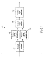
- Figure 1 shows the block diagram of a system 10 in accordance with an embodiment of the present invention.
- signed binary data is received by a signed binary thermometer encoder 12 that provides signed thermometer data to both a random barrel shifter for positive data 14, and a random barrel shifter for negative data 16.
- the output of each of the random barrel shifters 14 and 16 is provided to a tri-level logic shuffler 18, and the signed shuffled thermometer data that is output by the shuffler 18 is provided to a control logic decoder 20, which provides control signals to the DAC.
- the shuffler has two functions. First it selects the elements so that the average contribution of the error of each element is zero. Second, the average usage of each element compared to all other elements is kept equal. The first function is achieved by the a shuffler cell in accordance with an embodiment of the present invention while the second function is achieved by the butterfly connection in the overall shuffler. By shuffling the usage of the elements in a data-directed manner, the mismatch error is converted to noise and shaped to out-of-band frequency region.
- the present invention also provides for two barrel shifters that are controlled by a random number generator. These barrel shifters act to de-correlate the digital input signal of the shuffler so that idle tones are not generated by the shuffler cells.
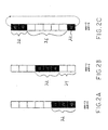
- Figures 2A, 2B and 2C show the operation of a 3-bit random barrel shifter when the data is 3 and the shift is 0, 2 and 6 respectively.
- the data is a code of 3 as shown at 22, and the shift control, which is generated by a pseudo-random generator, is 0, the data will occupy the bottom 3 bits.
- the shift control is greater than 0, data will be shifted up by the corresponding number of positions (e.g., 2 or 6 as shown in at 24 and 26 in Figures 2B and 2C ) and will wrap around if necessary as shown in Figure 2C .
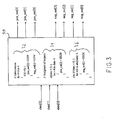
- Figure 3 shows the 3-bit signed thermometer logic encoder 30 with a descriptive depiction of the code provided therein for illustrative purposes.
- the input data is signed binary data (including a sign bit data[2] and a magnitude bit data[1] as well as a zero bit data[0] ), while the output data is signed thermometer data (including pos_out[0] , pas_out[1] , pos_out[2] , neg_out[0] , neg_out[1] , neg_out[2] and neg_out[3] ).
- both the positive outputs and negative outputs are first initialized to 0, then depending on the input data value, either the positive output bits or negative output bits are asserted 1 as shown at 34 and 36 respectively. There is never the case where both positive and negative outputs are asserted since this represents an illegal condition.
- FIG. 4 shows a schematic diagram of a shuffler cell 40 in accordance with an embodiment of the invention.
- the shuffler cell 40 includes D flip flops 42 and 44 that receive a clock input signal and current_state_a and current_state_b signals at inputs 46 and 48 respectively.
- the Q outputs of each of the flip flops 42 and 44 are provided to NOR gates 50 and 52 together with the Q ⁇ outputs of the other respective flip flop as shown.
- the Q output of the flip flop, 42 provides the next_state_a and the Q output of the flip flop 44 provides the next_state_b.
- the output of the NOR gate 50 is provided to an exclusive OR (XOR) gate 54 together with the a_in_pos data, and the output of the NOR gate 52 is provided to an XOR gate 56 together with the a_in_neg data.
- the output of the XOR gate 54 is provided to an XOR gate 58 together with the b_in_pos data, and the output of the XOR gate 56 is provided to an XOR gate 60 together with the b_in_neg data.
- the output of the XOR gate 58 is provided to both an AND gate 62 and to a NAND gate 64.
- the output of the XOR gate 60 is provided to an AND gate 66 and is also provided to the NAND gate 64.
- the output of the NAND gate 64 is provided to inputs of both of the AND gates 62 and 66.
- the outputs of the AND gates 62 and 66 are provided to the D inputs 46 and 48 of the flip flops 42 and 44 respectively.
- the a/b equalization for the positive and negative circuits is provided by summers 72, 74, 76 and 78.
- the output of the XOR gate 54 provides a swap_pos signal to clock signals of the summers 70 and 72
- the XOR gate 56 provides a swap_neg signal to the clock signals of the summers 74 and 76.
- the operation of the shuffler cell 40 is as follows. On the rising edge of the clock the state variable state_a and state_b are updated. Variable state_a records which of the 2 positive outputs was used previously while state_b records which of the 2 negative outputs was used previously. Specifically, if state_a is 1, a_out_pos was used previously. Likewise, if state_b is 1, a_out_neg was used previously. When both state_a and state_b are 1s, they indicate that a_out_pos and a_ont_neg were both used previously, this means that the error contributed by the element connected to a_out_pos and a_out_neg is averaged out and equal to zero.
- the truth table for valid values of the logic circuit for the shuffler cell 40 of Figure 4 is shown at 80 in Figures 5 . Although there are 64 total combinations of inputs, certain combinations are not permitted since they have both positive and negative inputs being 1s' at the same time, or state_a and state_b are both equal to 1s' at the same time.
- the valid input possible combinations are shown at 82 and the valid possible output combinations are shown at 84.
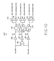
- Figure 6 shows a 3-bit tri-level logic shuffler that receives eight lines of input and produces eight lines of output.
- the cell employs a butterfly connection in which pairs of data lines are cross coupled as shown.
- circuit includes a swap cell 90 that receives input data neg_in[3], pos_in[3], neg_in[2] and pos_in[2].
- the swap cell 92 receives input data neg_in[1], pos_in[1], neg_in[0] and pos_in[0].
- the a_out_neg data and the a_out_pos data from the cell 90 are transferred directly a_in_neg and a_in_pos inputs of a cell 94, while the_bout_neg data and the b_out_neg data and the b_out_pos data from the cell 90 are crossed to a_in_neg and a_in_pos inputs of a cell 96.
- a_out_neg data and the a_out_pos data from the cell 90 are crossed to the b_in_neg and b_in_pos inputs of a cell 94, while the b_out_neg data and the b_out_pos data from the cell 90 are transferred directly to b_in_neg and b_in_pos inputs of cell 96.
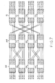
- Figure 7 shows a 4-bit tri-level logic shuffler circuit that receives eight pairs of inputs and produces 8 pairs of outputs.
- the circuit includes swap cells 100, 102, 108 and 110 that function as discussed above with respect to the circuit of Figure 6 .
- the circuit also includes cells 104, 106, 112 and 114 that also function as discussed above with respect to Figure 6 .
- a second stage is also provided in the circuit of Figure 7 in which the b_out_neg and b_out_pos data are provided directly to the cells 116, 118, 120 and 122 respectively, but the a_out_neg and a_out_pos data are crossed.
- the a_out_neg and a_out_pos data of the cell 108 are crossed to the a_in_neg and a_in_pos data inputs of the cell 120; the a_out_neg and a_out_pos data of the cell 110 are crossed to the a_in_neg and a_in_pos data inputs of the cell 122; the a_out_neg and a_out_pos data of the cell 112 are crossed to the a_in_neg and a_in_pos data inputs of the cell 116; and the a_out_neg and a_out_pos data of the cell 114 are crossed to the a_in_neg and a_in_pos data inputs of the cell 118. Since each shuffler has 4 outputs, it will be connected, therefore, to 2 pairs of push-pull current cells.
- Figure 8 shows a DAC cell 130 in accordance with an embodiment of the invention that includes an amplifier 132, a positive current source 134, a negative current source 136, and switches 138, 140, 142, 144, 146 and 148 that are employed to provide the BIT_PMOS, BITB_PMOS, BITB_NMOS and BIT_MOS outputs as shown.
- Figure 9 shows a DAC cell 150 in accordance with an embodiment of the invention that employs a NOR gate based design.
- the circuit 150 includes NOR gates 152, 160, 162 and 164, as well as buffers 154, 156, 158, 168, 172 and 176, and inverters 166, 170 and 174.
- Figure 10 shows a DAC cell 180 in accordance with another embodiment of the invention that employs a NAND gate based design.
- the circuit 180 includes a NOR gate 182 and NAND gates 190, 192 and 194, as well as buffers 184, 186, 188, 196, 200, 204, as well as inverters 198, 202 and 206.
- Figure 11 shows spectral plot of the output of a 2 nd -order , 4-bit DAC in accordance with a tri-level logic data-directed shuffler of an embodiment of the invention.
- the DAC has 16 unit elements that have a mismatch error of 0.5% rms.
- Figure 11 shows the 40dB/dec from the 2 nd order noise shaper at 210 and the 20dB/dec from element mismatch noise shaping at 212.
- Figure 12 shows a -60dBFS output of the same converter.
- Figure 12 shows the -100 to -50 dBFS at 214 to 50 dBFS at 214 with a peak shown at 216, with the simulation results with element mismatch shown at 220 and the ideal results without element mismatch shown at 218.
- Both Figures 11 and 12 show the noise shaping effect of the shuffler as a 20dB/dec slope of the spectral plots.
- the invention provides a method of generating a signed thermometer data output from a signed binary data input in which the method includes the step of generating two thermometer data outputs is provided, one thermometer data output; responding to positive input data and one responding to negative input data.
- a method of pre-randomizing the positive and negative thermometer data groups is provided, and may further include the steps of generating a pseudo-random number; and using the pseudo-random number to control two barrel shifters to shift the position of the thermometer data words within the barrel shifters.
- a method of grouping signed thermometer data before they enter a shuffler si includes the steps of paring the positive thermometer data into groups of two; and pairing the negative thermometer data into groups of two.
- a method of shuffling signed thermometer data includes the steps of generating a shuffler cell; generating the state variables, and a swap control signal within said shuffler cell based on the previous state variables and the current inputs; connecting the inputs of the shuffler cell directly to the outputs; or swapping the inputs before connecting them to the outputs according to the value of the swap control signal.
- the invention provides a signed thermometer data shuffler cell that includes a pair of positive thermometer data inputs, a pair of negative thermometer data inputs, a pair of positive thermometer data outputs , a pair of negative thermometer data outputs, and a clock signal and a reset signal.
- the invention further provides that the positive output pair of the previous shuffler cell may be connected to the positive input pair of the following shuffler cell; and that the negative output pair of the previous shuffler cell may be connected to the negative input pair of the following shuffler cell; wherein both connections follow the butterfly-style connection discussed above.
- a method of decoding the output of the shuffler includes the steps of generating a new control signal from the positive and negative inputs where the control signal is asserted when both inputs are low; connecting the control, signal to a pair of switches; connecting the positive input to a pair of switch; and connecting the negative input to a pair of switches.
- a method of holding the drain voltage of the current sources at a known level includes the step of connecting the current sources to a reference voltage buffer output when the input control signals are both zero.
Landscapes
- Engineering & Computer Science (AREA)
- Theoretical Computer Science (AREA)
- Compression, Expansion, Code Conversion, And Decoders (AREA)
- Communication Control (AREA)
- Analogue/Digital Conversion (AREA)
Claims (7)
- System (10) zur Verarbeitung digitaler Signale in einem Datenkonverter, wobei das System enthält:einen Thermometerkodierer (12, 30) zur Aufnahme von Binärdaten (data[0], data[1], data[2]) und zur Bereitstellung von Thermometerdaten,einen Mischer (18, 40), der positive und negative Eingangsdaten aufnimmt,einen Dekodierer (20) zur Aufnahme von Ausgangsdaten vom Mischer und Liefern von dekodierten Daten an eine analoge Stufe,wobei das System darüber hinaus dadurch gekennzeichnet ist, dassdie Binärdaten (data[0], data[1], data[2]) vorzeichenbehaftet sind und positive Thermometerdaten (pos_out[0], pos_out[1], pos_out[2]) und negative Thermometerdaten (neg_out[0], neg_out[1], neg_out[2], neg_out[3]), wobei die positiven Thermometerdaten (pos_out[0], pos_out[1], pos_out[2]) die Binärdaten (data[0], data[1], data[2]) über null repräsentieren und die negativen Thermometerdaten (neg_out[0], neg_out[1], neg_out[2], neg_out[3]) die Binärdaten (data[0], data[1], data[2]) unter null repräsentieren,der Mischer (18, 40) die auf die positiven Thermometerdaten (pos_out[0], pos_out[1], pos_out[2]) ansprechenden positiven Eingangsdaten aufnimmt und die auf die negativen Thermometerdaten (neg_out[0], neg_out[1], neg_out[2], neg_out[3]) ansprechenden negativen Eingangsdaten aufnimmt,und wobei das System (10) darüber hinaus einen zwischen dem Thermometerkodierer (12, 30) und dem Mischer (18, 40) angeordneten Positivdaten-Barrel-Shifter (14) und einen zwischen dem Thermometerkodierer (12, 30) und dem Mischer (18, 40) angeordneten Negativdaten-Barrel-Shifter (16) enthält.
- System nach Anspruch 1, bei dem der Mischer (18, 40) eine Vielzahl von Mischerzellen (40) enthält, von denen jede zwei Paare von Eingaben aufnimmt und zwei Paare von Ausgaben bereitstellt, wobei eines der Paare von Ausgaben an eine zweite Mischerzelle gekoppelt ist, während ein zweites der Paare von Ausgaben an eine dritte Mischerzelle gekoppelt ist.
- System nach Anspruch 2, bei dem der Mischer (18, 40) vier Paare von Dateneingaben (pos_in[0], neg_in[0], pos_in[1], neg_in[1], pos_in[2], neg_in[2], pos_in[3], neg_in[3]) aufnimmt und vier Paare von Datenausgaben (pos_out[0], pos_out[1], pos_out[2], pos_out[3], neg_out[0], neg_out[1], neg_out[2], neg_out[3]) bereitstellt.
- System nach Anspruch 2, bei dem jede Mischerzelle (40) ein Paar von positiven Thermometerdateneingaben, ein Paar von negativen Thermometerdateneingaben, ein Paar von positiven Thermometerdatenausgaben, ein Paar von negativen Thermometerdatenausgaben, ein Taktsignal und ein Rückstellsignal enthält.
- System nach Anspruch 2, bei dem jede Mischerzelle (40) Flipflops (42, 44) enthält.
- System nach Anspruch 1, bei dem die analoge Ausgangsstufe eine Drei-Ebenen-Logik-Ausgangstreiber (180) enthält, der eine positive Ausgabe (BIT_PMOS, BITB PMOS), eine negative Ausgabe (BIT NMOS, BITB_NMOS) und eine Nullausgabe (ZERO_PMOS, ZERO_NMOS) bereitstellt.
- System nach Anspruch 2, bei dem der Mischer (18, 40) acht Paare von Dateneingaben (pos_in[0], neg_in[0], pos_in[1], neg_in[1], pos_in[2], neg_in[2], pos_in[3], neg_in[3], pos_in[4], neg_in[4], pos_in[5], neg_in[5], pos_in[6], neg_in[6], pos_in[7], neg_in[7]) aufnimmt und acht Paare von Datenausgaben (pos_out[0], neg_out[0], pos_out[1], neg_out[1], pos_out[2], neg_out[2], pos_out[3], neg_out[3], pos_out[4], neg_out[4], pos_out[5], neg_out[5], pos_out[6], neg_out[6], pos_out[7], neg_out[7]) bereitstellt.
Applications Claiming Priority (2)
| Application Number | Priority Date | Filing Date | Title |
|---|---|---|---|
| US11/108,443 US7079063B1 (en) | 2005-04-18 | 2005-04-18 | System and method for tri-level logic data shuffling for oversampling data conversion |
| PCT/US2006/013761 WO2006113299A1 (en) | 2005-04-18 | 2006-04-13 | System and method for tri-level logic data shuffling for oversampling data conversion |
Publications (2)
| Publication Number | Publication Date |
|---|---|
| EP1872477A1 EP1872477A1 (de) | 2008-01-02 |
| EP1872477B1 true EP1872477B1 (de) | 2010-09-29 |
Family
ID=36659126
Family Applications (1)
| Application Number | Title | Priority Date | Filing Date |
|---|---|---|---|
| EP06749962A Not-in-force EP1872477B1 (de) | 2005-04-18 | 2006-04-13 | System und verfahren zum mischen logischer daten auf drei ebenen zur überabtastungsdatenkonvertierung |
Country Status (7)
| Country | Link |
|---|---|
| US (1) | US7079063B1 (de) |
| EP (1) | EP1872477B1 (de) |
| JP (2) | JP5063588B2 (de) |
| CN (1) | CN101160723B (de) |
| AT (1) | ATE483276T1 (de) |
| DE (1) | DE602006017193D1 (de) |
| WO (1) | WO2006113299A1 (de) |
Families Citing this family (21)
| Publication number | Priority date | Publication date | Assignee | Title |
|---|---|---|---|---|
| US7705757B2 (en) * | 2007-11-30 | 2010-04-27 | Analog Devices, Inc. | Gain matching method and system for single bit gain ranging analog-to-digital converter |
| US7679539B2 (en) * | 2008-03-25 | 2010-03-16 | Megawin Technology Co., Ltd. | Randomized thermometer-coding digital-to-analog converter and method therefor |
| US7777658B2 (en) * | 2008-12-12 | 2010-08-17 | Analog Devices, Inc. | System and method for area-efficient three-level dynamic element matching |
| EP2237424B1 (de) * | 2009-03-30 | 2013-02-27 | Dialog Semiconductor GmbH | Dynamische Elementanpassung für Dreipegelelemente, welche eine reduzierte Referenzladung und eine Reduzierung der Anzahl der DAW-Elemente erlaubt |
| US8085177B2 (en) | 2009-09-22 | 2011-12-27 | Mediatek Singapore Pte. Ltd. | Digital to analog converter system and method with multi-level scrambling |
| US8022850B2 (en) * | 2009-09-25 | 2011-09-20 | Freescale Semiconductor, Inc. | Multiple-bit, digital-to-analog converters and conversion methods |
| EP2391014B1 (de) * | 2009-12-09 | 2017-12-27 | Trigence Semiconductor, Inc. | Auswahlvorrichtung |
| US8847807B2 (en) | 2012-11-26 | 2014-09-30 | Analog Devices, Inc. | Switching scheme for ISI mitigation in data converters |
| US8842032B2 (en) | 2012-11-30 | 2014-09-23 | Analog Devices, Inc. | Enhanced second order noise shaped segmentation and dynamic element matching technique |
| US9065477B2 (en) | 2013-09-03 | 2015-06-23 | Analog Devices Global | Linear and DC-accurate frontend DAC and input structure |
| US9065463B2 (en) | 2013-10-11 | 2015-06-23 | Analog Devices Global | Method and apparatus for reducing capacitor induced ISI in DACS |
| EP2993787B1 (de) | 2014-09-05 | 2020-07-15 | Dialog Semiconductor (UK) Ltd | Verallgemeinertes datengewichtetes Mittelwertbildungsverfahren für gleichmäßig gewichtete Mehrbit-D/A-Elemente |
| US9397676B1 (en) | 2015-09-29 | 2016-07-19 | Analog Devices, Inc. | Low power switching techniques for digital-to-analog converters |
| CN106888016B (zh) * | 2015-12-15 | 2018-12-04 | 深圳市中兴微电子技术有限公司 | 一种电流舵数模转换器及电流舵数模转化方法 |
| US10187230B1 (en) * | 2017-09-08 | 2019-01-22 | Inphi Corporation | Equalization for transmitter input buffer array |
| KR102440369B1 (ko) | 2018-01-22 | 2022-09-05 | 삼성전자주식회사 | 3단 셀들을 사용하는 디지털-아날로그 변환을 위한 회로 및 방법 |
| US10581448B1 (en) * | 2018-05-28 | 2020-03-03 | Ali Tasdighi Far | Thermometer current mode analog to digital converter |
| CN108847849B (zh) * | 2018-07-25 | 2021-06-01 | 北京隆普智能科技有限公司 | 一种基本编解码单元以及编解码器 |
| US10819365B1 (en) | 2020-02-06 | 2020-10-27 | Analog Devices, Inc. | Utilizing current memory property in current steering digital-to-analog converters |
| US11658678B2 (en) | 2020-08-10 | 2023-05-23 | Analog Devices, Inc. | System and method to enhance noise performance in a delta sigma converter |
| US11757466B2 (en) | 2020-08-10 | 2023-09-12 | Analog Devices, Inc. | System and method for dynamic element matching for delta sigma converters |
Family Cites Families (12)
| Publication number | Priority date | Publication date | Assignee | Title |
|---|---|---|---|---|
| EP0265637B1 (de) * | 1986-09-26 | 1993-03-31 | Siemens Aktiengesellschaft | Impulsformer |
| JP2874218B2 (ja) * | 1989-10-20 | 1999-03-24 | ソニー株式会社 | A−dコンバータ |
| US5404142A (en) * | 1993-08-05 | 1995-04-04 | Analog Devices, Incorporated | Data-directed scrambler for multi-bit noise shaping D/A converters |
| EP1071218B1 (de) * | 1999-07-19 | 2009-09-09 | Texas Instruments Inc. | Differenzielle monadische Kodierung für digitales Audiosignal |
| US6414615B1 (en) | 2000-03-22 | 2002-07-02 | Raytheon Company | Excess delay compensation in a delta sigma modulator analog-to-digital converter |
| EP1139571B1 (de) * | 2000-03-31 | 2005-11-16 | Texas Instruments Incorporated | Pulsbreitenmodulation-D/A-Wandler |
| IT1320694B1 (it) * | 2000-10-06 | 2003-12-10 | St Microelectronics Srl | Metodo di equalizzazione dinamica degli elementi di un convertitoredigitale/analogico multibit integrato con uscita bilanciata per |
| US6518899B2 (en) * | 2001-06-13 | 2003-02-11 | Texas Instruments Incorporated | Method and apparatus for spectral shaping of non-linearity in data converters |
| US6762702B2 (en) * | 2002-01-24 | 2004-07-13 | Broadcom Corporation | Shuffler apparatus and related dynamic element matching technique for linearization of unit-element digital-to-analog converters |
| US6614377B1 (en) * | 2002-02-08 | 2003-09-02 | Analog Devices, Inc. | Data-directed scrambler for noise-shaping mixed-signal converters with an arbitrary number of quantization levels |
| KR20030086896A (ko) * | 2002-05-03 | 2003-11-12 | 톰슨 라이센싱 소시에떼 아노님 | 온도계 코드 디지털-오디오 변환기 |
| KR100555498B1 (ko) * | 2003-04-18 | 2006-03-03 | 삼성전자주식회사 | 데이터 전송속도를 향상시키는 송신기, 수신기 및 이를포함하는 데이터 인터페이스 시스템 |
-
2005
- 2005-04-18 US US11/108,443 patent/US7079063B1/en active Active
-
2006
- 2006-04-13 AT AT06749962T patent/ATE483276T1/de not_active IP Right Cessation
- 2006-04-13 WO PCT/US2006/013761 patent/WO2006113299A1/en active Application Filing
- 2006-04-13 EP EP06749962A patent/EP1872477B1/de not_active Not-in-force
- 2006-04-13 DE DE602006017193T patent/DE602006017193D1/de active Active
- 2006-04-13 CN CN200680012171XA patent/CN101160723B/zh not_active Expired - Fee Related
- 2006-04-13 JP JP2008507720A patent/JP5063588B2/ja not_active Expired - Fee Related
-
2011
- 2011-02-09 JP JP2011025601A patent/JP4991012B2/ja not_active Expired - Fee Related
Also Published As
| Publication number | Publication date |
|---|---|
| CN101160723B (zh) | 2012-05-23 |
| US7079063B1 (en) | 2006-07-18 |
| ATE483276T1 (de) | 2010-10-15 |
| EP1872477A1 (de) | 2008-01-02 |
| JP4991012B2 (ja) | 2012-08-01 |
| JP2011125062A (ja) | 2011-06-23 |
| JP5063588B2 (ja) | 2012-10-31 |
| WO2006113299A1 (en) | 2006-10-26 |
| DE602006017193D1 (de) | 2010-11-11 |
| JP2008538483A (ja) | 2008-10-23 |
| CN101160723A (zh) | 2008-04-09 |
Similar Documents
| Publication | Publication Date | Title |
|---|---|---|
| EP1872477B1 (de) | System und verfahren zum mischen logischer daten auf drei ebenen zur überabtastungsdatenkonvertierung | |
| US7777658B2 (en) | System and method for area-efficient three-level dynamic element matching | |
| Galton | Why dynamic-element-matching DACs work | |
| US6531973B2 (en) | Sigma-delta digital-to-analog converter | |
| US5221926A (en) | Circuit and method for cancelling nonlinearity error associated with component value mismatches in a data converter | |
| EP1819044B1 (de) | Mehrpegelquantisierer mit Current-Mode-DEM-Schaltmatrizen und separater DEM-Entscheidungslogik für einen Multibit-Sigma-Delta-Modulator | |
| Luschas et al. | Radio frequency digital-to-analog converter | |
| EP2449681B1 (de) | Stromgesteuerter digital analog wandler | |
| CN101964663B (zh) | 分段数模转换器 | |
| Shen et al. | Random swapping dynamic element matching technique for glitch energy minimization in current-steering DAC | |
| US20020171573A1 (en) | Method and apparatus for cyclic return to zero techniques for digital to analog convertors | |
| EP1331741B1 (de) | Umordnungsgerät mit entsprechender dynamischer Elementanpassungstechnik zur Linearisierung von Digital-Analog-Wandlern mit Einheitselementen | |
| Lee et al. | Advancing data weighted averaging technique for multi-bit sigma–delta modulators | |
| US9331710B1 (en) | Method and apparatus for encoding digital data into an oversampling digital to analog converter | |
| US7205913B2 (en) | Efficient data-directed scrambler for noise-shaping mixed-signal converters | |
| O'Brien et al. | High order mismatch shaping for low oversampling rates | |
| Venerus et al. | Simplified logic for tree-structure segmented DEM encoders | |
| Hsieh et al. | A first-order tree-structured DAC with reduced signal-band noise | |
| Chen et al. | A symmetric group control dynamic element matching method applied in high resolution SAR ADCs for biomedical applications | |
| O'Brien et al. | High order mismatch noise shaping for bandpass DACs | |
| Sanyal et al. | A simple and efficient dithering method for vector quantizer based mismatch-shaped ΔΣ DACs | |
| Tamura et al. | A multi-stage second order dynamic element matching with In-band mismatch noise reduction enhancement | |
| Andersson et al. | Dynamic element matching in decomposed digital-to-analog converters | |
| WO2018103866A1 (en) | Digital-to-analog converter with conversion cells converting ternary signal pairs |
Legal Events
| Date | Code | Title | Description |
|---|---|---|---|
| PUAI | Public reference made under article 153(3) epc to a published international application that has entered the european phase |
Free format text: ORIGINAL CODE: 0009012 |
|
| 17P | Request for examination filed |
Effective date: 20071018 |
|
| AK | Designated contracting states |
Kind code of ref document: A1 Designated state(s): AT BE BG CH CY CZ DE DK EE ES FI FR GB GR HU IE IS IT LI LT LU LV MC NL PL PT RO SE SI SK TR |
|
| 17Q | First examination report despatched |
Effective date: 20080411 |
|
| DAX | Request for extension of the european patent (deleted) | ||
| GRAP | Despatch of communication of intention to grant a patent |
Free format text: ORIGINAL CODE: EPIDOSNIGR1 |
|
| GRAS | Grant fee paid |
Free format text: ORIGINAL CODE: EPIDOSNIGR3 |
|
| GRAA | (expected) grant |
Free format text: ORIGINAL CODE: 0009210 |
|
| AK | Designated contracting states |
Kind code of ref document: B1 Designated state(s): AT BE BG CH CY CZ DE DK EE ES FI FR GB GR HU IE IS IT LI LT LU LV MC NL PL PT RO SE SI SK TR |
|
| REG | Reference to a national code |
Ref country code: GB Ref legal event code: FG4D |
|
| REG | Reference to a national code |
Ref country code: CH Ref legal event code: EP |
|
| REG | Reference to a national code |
Ref country code: IE Ref legal event code: FG4D |
|
| REF | Corresponds to: |
Ref document number: 602006017193 Country of ref document: DE Date of ref document: 20101111 Kind code of ref document: P |
|
| PG25 | Lapsed in a contracting state [announced via postgrant information from national office to epo] |
Ref country code: LT Free format text: LAPSE BECAUSE OF FAILURE TO SUBMIT A TRANSLATION OF THE DESCRIPTION OR TO PAY THE FEE WITHIN THE PRESCRIBED TIME-LIMIT Effective date: 20100929 Ref country code: AT Free format text: LAPSE BECAUSE OF FAILURE TO SUBMIT A TRANSLATION OF THE DESCRIPTION OR TO PAY THE FEE WITHIN THE PRESCRIBED TIME-LIMIT Effective date: 20100929 Ref country code: FI Free format text: LAPSE BECAUSE OF FAILURE TO SUBMIT A TRANSLATION OF THE DESCRIPTION OR TO PAY THE FEE WITHIN THE PRESCRIBED TIME-LIMIT Effective date: 20100929 |
|
| REG | Reference to a national code |
Ref country code: NL Ref legal event code: VDEP Effective date: 20100929 |
|
| LTIE | Lt: invalidation of european patent or patent extension |
Effective date: 20100929 |
|
| PG25 | Lapsed in a contracting state [announced via postgrant information from national office to epo] |
Ref country code: SI Free format text: LAPSE BECAUSE OF FAILURE TO SUBMIT A TRANSLATION OF THE DESCRIPTION OR TO PAY THE FEE WITHIN THE PRESCRIBED TIME-LIMIT Effective date: 20100929 |
|
| PG25 | Lapsed in a contracting state [announced via postgrant information from national office to epo] |
Ref country code: LV Free format text: LAPSE BECAUSE OF FAILURE TO SUBMIT A TRANSLATION OF THE DESCRIPTION OR TO PAY THE FEE WITHIN THE PRESCRIBED TIME-LIMIT Effective date: 20100929 Ref country code: GR Free format text: LAPSE BECAUSE OF FAILURE TO SUBMIT A TRANSLATION OF THE DESCRIPTION OR TO PAY THE FEE WITHIN THE PRESCRIBED TIME-LIMIT Effective date: 20101230 Ref country code: SE Free format text: LAPSE BECAUSE OF FAILURE TO SUBMIT A TRANSLATION OF THE DESCRIPTION OR TO PAY THE FEE WITHIN THE PRESCRIBED TIME-LIMIT Effective date: 20100929 |
|
| PG25 | Lapsed in a contracting state [announced via postgrant information from national office to epo] |
Ref country code: CZ Free format text: LAPSE BECAUSE OF FAILURE TO SUBMIT A TRANSLATION OF THE DESCRIPTION OR TO PAY THE FEE WITHIN THE PRESCRIBED TIME-LIMIT Effective date: 20100929 Ref country code: PT Free format text: LAPSE BECAUSE OF FAILURE TO SUBMIT A TRANSLATION OF THE DESCRIPTION OR TO PAY THE FEE WITHIN THE PRESCRIBED TIME-LIMIT Effective date: 20110131 Ref country code: NL Free format text: LAPSE BECAUSE OF FAILURE TO SUBMIT A TRANSLATION OF THE DESCRIPTION OR TO PAY THE FEE WITHIN THE PRESCRIBED TIME-LIMIT Effective date: 20100929 Ref country code: EE Free format text: LAPSE BECAUSE OF FAILURE TO SUBMIT A TRANSLATION OF THE DESCRIPTION OR TO PAY THE FEE WITHIN THE PRESCRIBED TIME-LIMIT Effective date: 20100929 Ref country code: IT Free format text: LAPSE BECAUSE OF FAILURE TO SUBMIT A TRANSLATION OF THE DESCRIPTION OR TO PAY THE FEE WITHIN THE PRESCRIBED TIME-LIMIT Effective date: 20100929 Ref country code: SK Free format text: LAPSE BECAUSE OF FAILURE TO SUBMIT A TRANSLATION OF THE DESCRIPTION OR TO PAY THE FEE WITHIN THE PRESCRIBED TIME-LIMIT Effective date: 20100929 Ref country code: RO Free format text: LAPSE BECAUSE OF FAILURE TO SUBMIT A TRANSLATION OF THE DESCRIPTION OR TO PAY THE FEE WITHIN THE PRESCRIBED TIME-LIMIT Effective date: 20100929 Ref country code: IS Free format text: LAPSE BECAUSE OF FAILURE TO SUBMIT A TRANSLATION OF THE DESCRIPTION OR TO PAY THE FEE WITHIN THE PRESCRIBED TIME-LIMIT Effective date: 20110129 |
|
| PG25 | Lapsed in a contracting state [announced via postgrant information from national office to epo] |
Ref country code: BE Free format text: LAPSE BECAUSE OF FAILURE TO SUBMIT A TRANSLATION OF THE DESCRIPTION OR TO PAY THE FEE WITHIN THE PRESCRIBED TIME-LIMIT Effective date: 20100929 |
|
| PG25 | Lapsed in a contracting state [announced via postgrant information from national office to epo] |
Ref country code: ES Free format text: LAPSE BECAUSE OF FAILURE TO SUBMIT A TRANSLATION OF THE DESCRIPTION OR TO PAY THE FEE WITHIN THE PRESCRIBED TIME-LIMIT Effective date: 20110109 |
|
| PLBE | No opposition filed within time limit |
Free format text: ORIGINAL CODE: 0009261 |
|
| STAA | Information on the status of an ep patent application or granted ep patent |
Free format text: STATUS: NO OPPOSITION FILED WITHIN TIME LIMIT |
|
| PG25 | Lapsed in a contracting state [announced via postgrant information from national office to epo] |
Ref country code: PL Free format text: LAPSE BECAUSE OF FAILURE TO SUBMIT A TRANSLATION OF THE DESCRIPTION OR TO PAY THE FEE WITHIN THE PRESCRIBED TIME-LIMIT Effective date: 20100929 Ref country code: DK Free format text: LAPSE BECAUSE OF FAILURE TO SUBMIT A TRANSLATION OF THE DESCRIPTION OR TO PAY THE FEE WITHIN THE PRESCRIBED TIME-LIMIT Effective date: 20100929 |
|
| REG | Reference to a national code |
Ref country code: DE Ref legal event code: R097 Ref document number: 602006017193 Country of ref document: DE Effective date: 20110630 |
|
| PG25 | Lapsed in a contracting state [announced via postgrant information from national office to epo] |
Ref country code: MC Free format text: LAPSE BECAUSE OF NON-PAYMENT OF DUE FEES Effective date: 20110430 |
|
| REG | Reference to a national code |
Ref country code: CH Ref legal event code: PL |
|
| REG | Reference to a national code |
Ref country code: FR Ref legal event code: ST Effective date: 20111230 |
|
| PG25 | Lapsed in a contracting state [announced via postgrant information from national office to epo] |
Ref country code: CH Free format text: LAPSE BECAUSE OF NON-PAYMENT OF DUE FEES Effective date: 20110430 Ref country code: LI Free format text: LAPSE BECAUSE OF NON-PAYMENT OF DUE FEES Effective date: 20110430 Ref country code: FR Free format text: LAPSE BECAUSE OF NON-PAYMENT OF DUE FEES Effective date: 20110502 |
|
| REG | Reference to a national code |
Ref country code: IE Ref legal event code: MM4A |
|
| PG25 | Lapsed in a contracting state [announced via postgrant information from national office to epo] |
Ref country code: IE Free format text: LAPSE BECAUSE OF NON-PAYMENT OF DUE FEES Effective date: 20110413 |
|
| PG25 | Lapsed in a contracting state [announced via postgrant information from national office to epo] |
Ref country code: CY Free format text: LAPSE BECAUSE OF FAILURE TO SUBMIT A TRANSLATION OF THE DESCRIPTION OR TO PAY THE FEE WITHIN THE PRESCRIBED TIME-LIMIT Effective date: 20100929 Ref country code: LU Free format text: LAPSE BECAUSE OF NON-PAYMENT OF DUE FEES Effective date: 20110413 |
|
| PG25 | Lapsed in a contracting state [announced via postgrant information from national office to epo] |
Ref country code: BG Free format text: LAPSE BECAUSE OF FAILURE TO SUBMIT A TRANSLATION OF THE DESCRIPTION OR TO PAY THE FEE WITHIN THE PRESCRIBED TIME-LIMIT Effective date: 20101229 Ref country code: TR Free format text: LAPSE BECAUSE OF FAILURE TO SUBMIT A TRANSLATION OF THE DESCRIPTION OR TO PAY THE FEE WITHIN THE PRESCRIBED TIME-LIMIT Effective date: 20100929 |
|
| PG25 | Lapsed in a contracting state [announced via postgrant information from national office to epo] |
Ref country code: HU Free format text: LAPSE BECAUSE OF FAILURE TO SUBMIT A TRANSLATION OF THE DESCRIPTION OR TO PAY THE FEE WITHIN THE PRESCRIBED TIME-LIMIT Effective date: 20100929 |
|
| PGFP | Annual fee paid to national office [announced via postgrant information from national office to epo] |
Ref country code: GB Payment date: 20210324 Year of fee payment: 16 |
|
| PGFP | Annual fee paid to national office [announced via postgrant information from national office to epo] |
Ref country code: DE Payment date: 20210323 Year of fee payment: 16 |
|
| REG | Reference to a national code |
Ref country code: DE Ref legal event code: R119 Ref document number: 602006017193 Country of ref document: DE |
|
| GBPC | Gb: european patent ceased through non-payment of renewal fee |
Effective date: 20220413 |
|
| PG25 | Lapsed in a contracting state [announced via postgrant information from national office to epo] |
Ref country code: GB Free format text: LAPSE BECAUSE OF NON-PAYMENT OF DUE FEES Effective date: 20220413 Ref country code: DE Free format text: LAPSE BECAUSE OF NON-PAYMENT OF DUE FEES Effective date: 20221103 |