EP1858308A1 - Multilayer printed wiring board - Google Patents
Multilayer printed wiring board Download PDFInfo
- Publication number
- EP1858308A1 EP1858308A1 EP06781090A EP06781090A EP1858308A1 EP 1858308 A1 EP1858308 A1 EP 1858308A1 EP 06781090 A EP06781090 A EP 06781090A EP 06781090 A EP06781090 A EP 06781090A EP 1858308 A1 EP1858308 A1 EP 1858308A1
- Authority
- EP
- European Patent Office
- Prior art keywords
- viaholes
- insulating
- printed wiring
- wiring board
- group
- Prior art date
- Legal status (The legal status is an assumption and is not a legal conclusion. Google has not performed a legal analysis and makes no representation as to the accuracy of the status listed.)
- Granted
Links
Images




Classifications
-
- H—ELECTRICITY
- H05—ELECTRIC TECHNIQUES NOT OTHERWISE PROVIDED FOR
- H05K—PRINTED CIRCUITS; CASINGS OR CONSTRUCTIONAL DETAILS OF ELECTRIC APPARATUS; MANUFACTURE OF ASSEMBLAGES OF ELECTRICAL COMPONENTS
- H05K3/00—Apparatus or processes for manufacturing printed circuits
- H05K3/40—Forming printed elements for providing electric connections to or between printed circuits
- H05K3/42—Plated through-holes or plated via connections
- H05K3/421—Blind plated via connections
-
- H—ELECTRICITY
- H05—ELECTRIC TECHNIQUES NOT OTHERWISE PROVIDED FOR
- H05K—PRINTED CIRCUITS; CASINGS OR CONSTRUCTIONAL DETAILS OF ELECTRIC APPARATUS; MANUFACTURE OF ASSEMBLAGES OF ELECTRICAL COMPONENTS
- H05K3/00—Apparatus or processes for manufacturing printed circuits
- H05K3/46—Manufacturing multilayer circuits
-
- H—ELECTRICITY
- H05—ELECTRIC TECHNIQUES NOT OTHERWISE PROVIDED FOR
- H05K—PRINTED CIRCUITS; CASINGS OR CONSTRUCTIONAL DETAILS OF ELECTRIC APPARATUS; MANUFACTURE OF ASSEMBLAGES OF ELECTRICAL COMPONENTS
- H05K1/00—Printed circuits
- H05K1/02—Details
- H05K1/11—Printed elements for providing electric connections to or between printed circuits
- H05K1/115—Via connections; Lands around holes or via connections
-
- H—ELECTRICITY
- H05—ELECTRIC TECHNIQUES NOT OTHERWISE PROVIDED FOR
- H05K—PRINTED CIRCUITS; CASINGS OR CONSTRUCTIONAL DETAILS OF ELECTRIC APPARATUS; MANUFACTURE OF ASSEMBLAGES OF ELECTRICAL COMPONENTS
- H05K3/00—Apparatus or processes for manufacturing printed circuits
- H05K3/46—Manufacturing multilayer circuits
- H05K3/4602—Manufacturing multilayer circuits characterized by a special circuit board as base or central core whereon additional circuit layers are built or additional circuit boards are laminated
-
- H—ELECTRICITY
- H05—ELECTRIC TECHNIQUES NOT OTHERWISE PROVIDED FOR
- H05K—PRINTED CIRCUITS; CASINGS OR CONSTRUCTIONAL DETAILS OF ELECTRIC APPARATUS; MANUFACTURE OF ASSEMBLAGES OF ELECTRICAL COMPONENTS
- H05K2201/00—Indexing scheme relating to printed circuits covered by H05K1/00
- H05K2201/03—Conductive materials
- H05K2201/0332—Structure of the conductor
- H05K2201/0388—Other aspects of conductors
- H05K2201/0394—Conductor crossing over a hole in the substrate or a gap between two separate substrate parts
-
- H—ELECTRICITY
- H05—ELECTRIC TECHNIQUES NOT OTHERWISE PROVIDED FOR
- H05K—PRINTED CIRCUITS; CASINGS OR CONSTRUCTIONAL DETAILS OF ELECTRIC APPARATUS; MANUFACTURE OF ASSEMBLAGES OF ELECTRICAL COMPONENTS
- H05K2201/00—Indexing scheme relating to printed circuits covered by H05K1/00
- H05K2201/09—Shape and layout
- H05K2201/09209—Shape and layout details of conductors
- H05K2201/095—Conductive through-holes or vias
- H05K2201/09563—Metal filled via
-
- H—ELECTRICITY
- H05—ELECTRIC TECHNIQUES NOT OTHERWISE PROVIDED FOR
- H05K—PRINTED CIRCUITS; CASINGS OR CONSTRUCTIONAL DETAILS OF ELECTRIC APPARATUS; MANUFACTURE OF ASSEMBLAGES OF ELECTRICAL COMPONENTS
- H05K2201/00—Indexing scheme relating to printed circuits covered by H05K1/00
- H05K2201/09—Shape and layout
- H05K2201/09209—Shape and layout details of conductors
- H05K2201/095—Conductive through-holes or vias
- H05K2201/096—Vertically aligned vias, holes or stacked vias
-
- H—ELECTRICITY
- H05—ELECTRIC TECHNIQUES NOT OTHERWISE PROVIDED FOR
- H05K—PRINTED CIRCUITS; CASINGS OR CONSTRUCTIONAL DETAILS OF ELECTRIC APPARATUS; MANUFACTURE OF ASSEMBLAGES OF ELECTRICAL COMPONENTS
- H05K2201/00—Indexing scheme relating to printed circuits covered by H05K1/00
- H05K2201/09—Shape and layout
- H05K2201/09209—Shape and layout details of conductors
- H05K2201/09654—Shape and layout details of conductors covering at least two types of conductors provided for in H05K2201/09218 - H05K2201/095
- H05K2201/09709—Staggered pads, lands or terminals; Parallel conductors in different planes
-
- H—ELECTRICITY
- H05—ELECTRIC TECHNIQUES NOT OTHERWISE PROVIDED FOR
- H05K—PRINTED CIRCUITS; CASINGS OR CONSTRUCTIONAL DETAILS OF ELECTRIC APPARATUS; MANUFACTURE OF ASSEMBLAGES OF ELECTRICAL COMPONENTS
- H05K2201/00—Indexing scheme relating to printed circuits covered by H05K1/00
- H05K2201/09—Shape and layout
- H05K2201/09818—Shape or layout details not covered by a single group of H05K2201/09009 - H05K2201/09809
- H05K2201/09863—Concave hole or via
-
- H—ELECTRICITY
- H05—ELECTRIC TECHNIQUES NOT OTHERWISE PROVIDED FOR
- H05K—PRINTED CIRCUITS; CASINGS OR CONSTRUCTIONAL DETAILS OF ELECTRIC APPARATUS; MANUFACTURE OF ASSEMBLAGES OF ELECTRICAL COMPONENTS
- H05K2203/00—Indexing scheme relating to apparatus or processes for manufacturing printed circuits covered by H05K3/00
- H05K2203/07—Treatments involving liquids, e.g. plating, rinsing
- H05K2203/0703—Plating
- H05K2203/0733—Method for plating stud vias, i.e. massive vias formed by plating the bottom of a hole without plating on the walls
-
- H—ELECTRICITY
- H05—ELECTRIC TECHNIQUES NOT OTHERWISE PROVIDED FOR
- H05K—PRINTED CIRCUITS; CASINGS OR CONSTRUCTIONAL DETAILS OF ELECTRIC APPARATUS; MANUFACTURE OF ASSEMBLAGES OF ELECTRICAL COMPONENTS
- H05K3/00—Apparatus or processes for manufacturing printed circuits
- H05K3/40—Forming printed elements for providing electric connections to or between printed circuits
- H05K3/42—Plated through-holes or plated via connections
- H05K3/423—Plated through-holes or plated via connections characterised by electroplating method
-
- H—ELECTRICITY
- H05—ELECTRIC TECHNIQUES NOT OTHERWISE PROVIDED FOR
- H05K—PRINTED CIRCUITS; CASINGS OR CONSTRUCTIONAL DETAILS OF ELECTRIC APPARATUS; MANUFACTURE OF ASSEMBLAGES OF ELECTRICAL COMPONENTS
- H05K3/00—Apparatus or processes for manufacturing printed circuits
- H05K3/46—Manufacturing multilayer circuits
- H05K3/4644—Manufacturing multilayer circuits by building the multilayer layer by layer, i.e. build-up multilayer circuits
- H05K3/4652—Adding a circuit layer by laminating a metal foil or a preformed metal foil pattern
-
- Y—GENERAL TAGGING OF NEW TECHNOLOGICAL DEVELOPMENTS; GENERAL TAGGING OF CROSS-SECTIONAL TECHNOLOGIES SPANNING OVER SEVERAL SECTIONS OF THE IPC; TECHNICAL SUBJECTS COVERED BY FORMER USPC CROSS-REFERENCE ART COLLECTIONS [XRACs] AND DIGESTS
- Y10—TECHNICAL SUBJECTS COVERED BY FORMER USPC
- Y10T—TECHNICAL SUBJECTS COVERED BY FORMER US CLASSIFICATION
- Y10T29/00—Metal working
- Y10T29/49—Method of mechanical manufacture
- Y10T29/49002—Electrical device making
- Y10T29/49117—Conductor or circuit manufacturing
- Y10T29/49124—On flat or curved insulated base, e.g., printed circuit, etc.
- Y10T29/49126—Assembling bases
-
- Y—GENERAL TAGGING OF NEW TECHNOLOGICAL DEVELOPMENTS; GENERAL TAGGING OF CROSS-SECTIONAL TECHNOLOGIES SPANNING OVER SEVERAL SECTIONS OF THE IPC; TECHNICAL SUBJECTS COVERED BY FORMER USPC CROSS-REFERENCE ART COLLECTIONS [XRACs] AND DIGESTS
- Y10—TECHNICAL SUBJECTS COVERED BY FORMER USPC
- Y10T—TECHNICAL SUBJECTS COVERED BY FORMER US CLASSIFICATION
- Y10T29/00—Metal working
- Y10T29/49—Method of mechanical manufacture
- Y10T29/49002—Electrical device making
- Y10T29/49117—Conductor or circuit manufacturing
- Y10T29/49124—On flat or curved insulated base, e.g., printed circuit, etc.
- Y10T29/49128—Assembling formed circuit to base
-
- Y—GENERAL TAGGING OF NEW TECHNOLOGICAL DEVELOPMENTS; GENERAL TAGGING OF CROSS-SECTIONAL TECHNOLOGIES SPANNING OVER SEVERAL SECTIONS OF THE IPC; TECHNICAL SUBJECTS COVERED BY FORMER USPC CROSS-REFERENCE ART COLLECTIONS [XRACs] AND DIGESTS
- Y10—TECHNICAL SUBJECTS COVERED BY FORMER USPC
- Y10T—TECHNICAL SUBJECTS COVERED BY FORMER US CLASSIFICATION
- Y10T29/00—Metal working
- Y10T29/49—Method of mechanical manufacture
- Y10T29/49002—Electrical device making
- Y10T29/49117—Conductor or circuit manufacturing
- Y10T29/49124—On flat or curved insulated base, e.g., printed circuit, etc.
- Y10T29/4913—Assembling to base an electrical component, e.g., capacitor, etc.
-
- Y—GENERAL TAGGING OF NEW TECHNOLOGICAL DEVELOPMENTS; GENERAL TAGGING OF CROSS-SECTIONAL TECHNOLOGIES SPANNING OVER SEVERAL SECTIONS OF THE IPC; TECHNICAL SUBJECTS COVERED BY FORMER USPC CROSS-REFERENCE ART COLLECTIONS [XRACs] AND DIGESTS
- Y10—TECHNICAL SUBJECTS COVERED BY FORMER USPC
- Y10T—TECHNICAL SUBJECTS COVERED BY FORMER US CLASSIFICATION
- Y10T29/00—Metal working
- Y10T29/49—Method of mechanical manufacture
- Y10T29/49002—Electrical device making
- Y10T29/49117—Conductor or circuit manufacturing
- Y10T29/49124—On flat or curved insulated base, e.g., printed circuit, etc.
- Y10T29/49155—Manufacturing circuit on or in base
-
- Y—GENERAL TAGGING OF NEW TECHNOLOGICAL DEVELOPMENTS; GENERAL TAGGING OF CROSS-SECTIONAL TECHNOLOGIES SPANNING OVER SEVERAL SECTIONS OF THE IPC; TECHNICAL SUBJECTS COVERED BY FORMER USPC CROSS-REFERENCE ART COLLECTIONS [XRACs] AND DIGESTS
- Y10—TECHNICAL SUBJECTS COVERED BY FORMER USPC
- Y10T—TECHNICAL SUBJECTS COVERED BY FORMER US CLASSIFICATION
- Y10T29/00—Metal working
- Y10T29/49—Method of mechanical manufacture
- Y10T29/49002—Electrical device making
- Y10T29/49117—Conductor or circuit manufacturing
- Y10T29/49124—On flat or curved insulated base, e.g., printed circuit, etc.
- Y10T29/49155—Manufacturing circuit on or in base
- Y10T29/49156—Manufacturing circuit on or in base with selective destruction of conductive paths
-
- Y—GENERAL TAGGING OF NEW TECHNOLOGICAL DEVELOPMENTS; GENERAL TAGGING OF CROSS-SECTIONAL TECHNOLOGIES SPANNING OVER SEVERAL SECTIONS OF THE IPC; TECHNICAL SUBJECTS COVERED BY FORMER USPC CROSS-REFERENCE ART COLLECTIONS [XRACs] AND DIGESTS
- Y10—TECHNICAL SUBJECTS COVERED BY FORMER USPC
- Y10T—TECHNICAL SUBJECTS COVERED BY FORMER US CLASSIFICATION
- Y10T29/00—Metal working
- Y10T29/49—Method of mechanical manufacture
- Y10T29/49002—Electrical device making
- Y10T29/49117—Conductor or circuit manufacturing
- Y10T29/49124—On flat or curved insulated base, e.g., printed circuit, etc.
- Y10T29/49155—Manufacturing circuit on or in base
- Y10T29/49165—Manufacturing circuit on or in base by forming conductive walled aperture in base
-
- Y—GENERAL TAGGING OF NEW TECHNOLOGICAL DEVELOPMENTS; GENERAL TAGGING OF CROSS-SECTIONAL TECHNOLOGIES SPANNING OVER SEVERAL SECTIONS OF THE IPC; TECHNICAL SUBJECTS COVERED BY FORMER USPC CROSS-REFERENCE ART COLLECTIONS [XRACs] AND DIGESTS
- Y10—TECHNICAL SUBJECTS COVERED BY FORMER USPC
- Y10T—TECHNICAL SUBJECTS COVERED BY FORMER US CLASSIFICATION
- Y10T428/00—Stock material or miscellaneous articles
- Y10T428/31504—Composite [nonstructural laminate]
- Y10T428/31511—Of epoxy ether
Definitions
- the present invention relates to a multilayer printed wiring board for mounting electronic components such as a capacitor, IC and the like on the surface layer thereof and further in detail relates to a multilayer printed wiring board which prevents the loss of electric components by dropping or lowering the electric connectivity and reliability.
- the recent portable electronic devices such as a mobile phone, digital camera, etc., have been improved to correspond to densification of surface-mounted components by solutions such as miniaturization of surface-mounted components meeting the requirements for highly sophistication and densification, increasing the density of wiring (by reducing the width of lines for wiring / the spaces between lines for wiring) on boards, reducing the sizes of solder pads and so on.
- the electronic components to be mounted on such a wiring board are passive parts such as an IC chip, capacitor, resistor, inductor and the like, a liquid crystal device, a display device for digital indication, control devices such as keypad, switches and the like or external terminals such as a USB, earphone and the like.
- a typical one of multilayer circuit boards on which the above electronic components are to be mounted discloses that holes for viaholes are formed, by lasering, in an insulating rigid substrate having a conductor circuit formed on one side or either side thereof, viaholes are formed by filling a metal paste or a plating material in the holes to form an interlayer-connected circuit board, and two or more such circuit boards prepared as above are stacked sequentially or collectively to produce a multilayer printed wiring board. (refer to Japanese Patent Laid Open No. 13028 of 1998 )
- two circuit boards are electrically connected to each other by connecting a viahole or a land of the viahole in one of the adjacent circuit boards to a conductor circuit or land of the other circuit board.
- circuit boards are joined, at other areas thereof not contributing to electrical connection between them, to each other with an adhesive layer, prepreg or the like of a thermosetting resin, to thereby form a multilayer structure.
- a solder resist layer to protect the conductor circuit is formed on the surface layer of the above multilayer circuit board or prevailing printed wiring board, a hole is formed in a part of the solder resist layer, and a corrosion-resistant layer of gold nickel-gold or the like is formed on the surface, exposed in the hole, of the conductor circuit.
- a solder piece such as a solder bump is formed on the surface, having the corrosion-resistant layer formed thereon, of the conductor circuit, and an electronic component such as a capacitor, IC or the like is mounted on the solder piece formed on the conductor circuit surface.
- the multilayer circuit board used in the aforementioned portable electronic device such as a mobile phone, digital camera or the like and having electronic components mounted thereon at a high density should further be improved in reliability.
- the multilayer circuit board or an electronic device product (using an encased circuit board having mounted thereon all electronic components including a liquid crystal device) is required to show higher reliability as provable by the dropping test, wherein functions of the board and the electric device are not decreased and furthermore the electric components will not drop off even if the board is dropped repeatedly a predetermined number times from a specific height.
- each insulating layer included in the printed circuit board is required to be 100 ⁇ m or less in thickness and even a multilayered circuit board is to be smaller in total thickness than ever. Therefore, the printed circuit board itself is likely to be lower in rigidity.
- the printed circuit board itself is lower in rigidity as above, its resistance against warp is lower with the result that the wiring board is likely to lose its flatness, which will cause an inconvenience in a subsequent process (in mounting electronic components, for example).
- the printed circuit board itself is also flexible, easily warped, and likely to be influenced by an external shock-caused stress. It is under consideration that, for example, a core one of insulating substrates for stacking the substrates together should be formed to be 600 ⁇ m or more in thickness to increase the rigidity of the wiring board. However, since the aforementioned multilayer printed wiring board having such an increased thickness cannot be housed in a case of a portable electronic device as the case may be, there is a dilemma that the insulating substrate as the core for stacking the insulating substrates together may not be increased in thickness.
- the rigidity thereof could not be improved by increasing the thickness of the insulating substrate as the core for stacking the substrates, it was difficult to provide a circuit board having an improved function and reliability, which is normally provable by the dropping test as one of the reliability tests.
- the conventional circuit board cannot have any further improved electrical connection and reliability.
- the inventors of the present invention have devoted themselves to the studies in this field of technology for implementing the above multilayer printed wiring board. Taking into consideration the shape and stacked pattern of viaholes electrically connecting conductor circuits to each other in a multilayer circuit board, the Inventors formed at least a part of the viahole to bulge in a direction generally orthogonal to the direction of thickness of the insulating layer. With this arrangement, the inventors found that the printed wiring board would not be reduced in rigidity, warped or otherwise influenced even if the insulating substrates included in the printed wiring board was reduced in thickness. Based on these findings, the inventors worked out the present invention, which will be described below.
- the insulating layer or insulating substrate may be 100 ⁇ m or less in thickness. Otherwise, the insulating layer or substrate may be 50 ⁇ m or less in thickness.
- the viaholes may be stacked on each other to form a multistage stacked via. Also, the viaholes formed in the insulating substrates stacked on one side of one of the insulating substrates having the conductor layer formed thereon are taken as a first group of viaholes, while those formed in the insulating substrates stacked on the other side of the one insulating layer are taken as a second group of viaholes.
- the first viahole group may be stacked on the second viahole group in such geometry that they are opposite to each other. Also, the first viahole group may be stacked on the second viahole group in such geometry that it is shifted in relation to the second viahole group in a direction generally orthogonal to the direction of thickness of the insulating layer.
- the viaholes in the first or second group may be stacked on almost same straight lines, respectively. Otherwise, the viaholes may be stacked together in such geometry that they are shifted from each other in a direction generally orthogonal to the direction of thickness of the insulating layer.
- the viaholes included in either the first or second group may also be positioned at two opposite apexes of an imaginary tetragonal lattice on the insulating substrate while the viaholes included in the other group may be positioned at other two opposite apexes of the imaginary tetragonal lattice on the insulating layer.
- the viaholes included in either the first or second group may also be positioned at apexes of an imaginary tetragonal or triangular lattice on the insulating substrate while the viaholes included in the other group may be positioned at the center of the imaginary tetragonal or triangular lattice on the insulating layer.
- the viaholes included in either the first or second group may also be positioned intensively in a predetermined area of the insulating substrate while the viaholes included in the other group may be positioned in a peripheral area surrounding the predetermined area of the insulating layer.
- Each of the viaholes may also be formed to bulge so that the diameter of a largest bulged part is 1.1 to 1.5 times larger than that of the hole in the top or bottom of the insulating layer.
- Each of the viaholes may also be formed by filling a plating material in a hole formed in the insulating layer or insulating substrate.
- the viahole electrically connecting the conductor layers to each other has a part thereof formed to bulge in a direction generally orthogonal to the direction of thickness of the insulating layer. So, the insulating layer can be prevented from being warped due to an external stress (such as an impact applied to the multilayer printed wiring board if dropped or the like).
- the viaholes can be stacked to form a multistage stacked via structure. So, in case the printed circuit board is applied with an external stress and the insulating layers are warped outwardly, the insulating resin layers and conductor layers forming the multistage stacked via are not easily separable from each other because the multistage stacked via will bite in the insulating layers. Thus, it is possible to prevent the printed circuit board from being reduced in reliability and drop-shock resistance.
- the multistage stacked via formed in the insulating layers will function as a stake to prevent the insulating layers or insulating substrate from being easily warped.
- the external stress transmitted to the insulating layer can be limited and thus the possible reduction of the reliability and drop-shock resistance of the printed circuit board can also be limited.
- the multistage stacked via since the multistage stacked via is formed within the insulating layer, it will function as a stake to prevent the insulating layers from being easily warped. Therefore, the substrates will be able to keep their flatness, so that the printed circuit board can maintain the reliability as provable by the reliability test such as a heat cycle test without any early cracking of the conductor circuits including the viaholes and insulating layers and any reduction in reliability of the printed circuit board.
- a printed circuit board can be formed by forming a conductor circuit on an insulating layer or substrate of 100 ⁇ m or less in thickness and stacking more than one such an insulating layer together.
- the printed circuit board can advantageously be prevented from being warped, namely, it can maintain its flatness. Even in case the insulating layer or substrate is 50 ⁇ m or less in thickness, a similar effect can be assured.
- the multistage stacked via (first and second viahole groups) formed in such geometry that the first and second viahole groups are opposite to each other effectively prevents the insulating layers from being warped both outwardly and inwardly of them. That is, even if the insulating layers are going to be warped when applied with an external stress, the multistage stacked via formed in the insulating layers will add to the resistance against both the outward and inward warp caused by the external stress. As a result, the printed circuit board will incur less reduction of its reliability and drop-shock resistance.
- the insulating layers themselves will be improved in rigidity in such an area where the multistage stacked vias are formed. Therefore, it is possible to reduce the warping itself of the printed circuit board, and the flatness of the printed circuit board can be maintained and mounted components will not drop off the printed circuit board in the subsequent processes (such as solder-resist forming step, solder layer forming step, electronic component mounting step, etc.). Thus, it is possible to make smaller the considerable reduction in electrical connection and reliability of the printed circuit board.
- the multilayer printed wiring board as an embodiment of the present invention is such that a viahole is formed in an insulating layer to electrically connect conductor layers formed on either side of the insulating layer to each other so that at least a part thereof bulges in a direction orthogonal to the direction of thickness of the insulating layer.
- the conductor circuit provided on the one insulating substrate and that provided on the other insulating substrate are electrically connected to each other through viaholes formed in the insulating substrates, respectively, and each of the viaholes is formed to have at least a part thereof bulged in a direction generally orthogonal to the direction of thickness of the insulating layer.
- the insulating layer or substrate used in the multilayer printed wiring board according to the present invention should be a rigid substrate selected from among, for example, glass cloth-based epoxy resin, phenol resin, glass cloth-based bismaleimide triazine resin, glass cloth-based polyphenylene ether resin, aramid unwoven cloth-based epoxy resin, aramid unwoven cloth-based polyamide resin, etc.
- the substrate of such an insulating resin should desirably be 100 ⁇ m or less in thickness. Also, the substrate of such an insulating resin may be 50 ⁇ m or less in thickness.
- a multilayer printed wiring board (printed circuit board) is formed by stacking such insulating layers or substrates alternately on the surface of a circuit board as the core of stacking, in which a conductor circuit is formed on one or both of the surfaces of the insulating layer or substrate. Also, the thickness of the multilayer printed circuit board itself can be reduced by reducing the thickness of all the insulating layers or substrates in such a printed circuit board to 100 ⁇ m or less.
- both the conductor circuits formed on the insulating substrates and the viaholes (multistage stacked via) included in the first and second groups should desirably be formed by plating.
- the reason is that, if the viaholes included in the first and second groups respectively and the connecting parts where the upper and lower surfaces of such viaholes contact with the conductor circuit respectively are formed by the coat of the same plating, there is hardly dropping off, and that even if the board receives the external stress from the lateral sides, the misalignment will not be caused and there is hardly cracking of the board.
- the viahole is formed by electrolytic or electroless plating.
- the metal used for plating may be an element such as copper, nickel, iron, cobalt or the like or an alloy based on any of the elements.
- the viahole in the embodiment of the present invention should desirably be formed to bulge in a direction generally orthogonal to the direction of thickness of the insulating layer, that is, it should desirably be formed to have a so-called barrel shape of which the diameter of an intermediate part thereof between the top and bottom is larger than those of the top and bottom.
- the viahole in such a barrel shape has the top and bottom being the smallest in diameter and is bulged for at least a part thereof, for example, at least a just intermediate part between the top and bottom, to be largest in diameter.
- the viahole bulging should desirably be such that the diameter at the intermediate part of the viahole is 1.1 to 1.5 times larger than the opening diameter (minimum) at the top or bottom, that is to say, such that on the assumption that the diameter at the top or bottom is D, the diameter at the part having the largest bulge is 1.1D to 1.5 D.
- the reason for the above is that, if the diameter at the part having the largest bulge is less than 1.1D, the viahole cannot be formed in a barrel shape and cannot perform its effect. Or if the diameter at the part having the largest bulge is more than 1.5D, an electrically conductive material such as a plating material cannot be easily filled into the viahole-forming hole, sometimes hardly assure an insulating gap in the interlaminar insulating layer between the adjacent viaholes and therefore the connectivity and reliability is decreased.
- the top of the viahole in the embodiment of the present invention should desirably have a diameter ranging from 50 to 250 ⁇ m.
- the reason for the above is that, if the top of the viahole has a diameter less than 50 ⁇ m, the conductor layer is hardly formed inside of via. Or if the top of the viahole has a diameter more than 250 ⁇ m, forming conductor layer into a via shape in the embodiment of the present invention (a part thereof bulged in a direction generally orthogonal to the direction of thickness of the insulating layer) might be failed easily and the gap with the adjacent via is hardly assured.
- the viahole diameter at the bottom (will be referred to as "via-bottom diameter” hereunder) may be at least 10 ⁇ m.
- the via-bottom diameter should be at least 10 ⁇ m for that plating, whereby the upper conductor layer (upper conductor circuit and viahole) and lower one can electrically be connected to each other.
- the multistage stacked via should preferably be formed for the bottoms of outer viaholes (upper viaholes) to be superposed on those of inner viaholes (lower viaholes) in the same position. That is, the viaholes in the first and second groups can be formed on almost same straight lines, respectively, as shown in Fig. 2.
- the viaholes may be stacked together in respective positions shifted in a direction orthogonal to each other in the direction of thickness of the insulating layers and where the bottoms of the viaholes overlap at least partially each other.
- the viaholes in the first or second group may be stacked in respective positions where they are shifted a half of their diameter from each other as shown in Fig. 3A. Also, the viaholes in the first or second group may be stacked in respective positions where they are shifted nearly one viahole diameter from each other as shown in Fig. 3B.
- the first or second group of viaholes included in the multistage stacked via should preferably be formed by providing at least two or more insulating substrates and stacking the viaholes formed in the insulating substrates together. That is, the first or second viahole group may be formed from three, four or more viahole layers by stacking them together.
- the first and second viaholes groups may be equal in number of viahole layers to each other (e.g., three viahole layers in the first group and three viahole layers in the second group) or may be different in number of viahole layers from each other (e.g., two viahole layers in the first group and three viahole layers in the second group).
- the interlayer electrical connection and reliability of the printed circuit board will not be decreased significantly by forming the first and second viahole groups in the multistage stacked via in such geometry that they are opposite to each other.
- the multistage stacked via may be an electrically conductive layer. But it may also be an electrically nonconductive layer, that is, a so-called dummy conductor layer.
- a so-called dummy conductor layer In case the multistage stacked via is formed from a dummy conductor layer, it will be assured that conductor layers other than the dummy layer (conductor layers formed around the dummy conductor layer or conductor layers electrically connected to each other by the viahole in the diagonally disposed multistage stacked via or the like) will not lower their reliability and drop-shock resistance. Also, the printed circuit board maintains its flatness since its warping can be minimized.
- the first and second viahole groups included in the multistage stacked via should desirably be disposed in generally same positions (on almost same lines) within an area where the conductor circuit of each insulating substrate is formed as shown in Fig. 2 or disposed in respective positions shifted from each other (dispersed disposition) as shown in Fig. 3A or 3B.
- the first and/or second viahole groups mainly in the central portion of the insulating substrate which is likely to be most influenced by an external stress it is possible toimprove a resistance of the insulating substrates against a warp of the insulating substrates caused by an external stress.
- first and/or second viahole groups may be disposed not in the central portion of the insulating substrate but mainly in a peripheral area surrounding that central portion. Such a disposition of the first and second viahole groups permits to assure the satisfactory resistance of the insulating substrates against the warp. Also it is possible to assure a satisfactory flatness of the printed circuit board.
- the first and second viahole groups may be disposed opposite to each other, while in the peripheral portion, the first and second viahole groups may be disposed in respective positions shifted from each other.
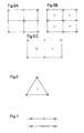
- the multistage stacked vias are disposed in any of various patterns of disposition in plane, such as a tetragonal lattice (as in Figs. 5A to 5C), triangular lattice (as in Fig. 6) or straight line (as in Fig. 7) in addition to the aforementioned patterns.
- a tetragonal lattice as in Figs. 5A to 5C
- triangular lattice as in Fig. 6
- straight line as in Fig. 7
- the viaholes are disposed as follows.
- the first and second viahole groups are disposed regularly in an imaginary tetragonal matrix as shown in Fig. 5A.
- the first viahole groups are disposed in an imaginary matrix while the second viahole groups opposite to the first ones are disposed in an intermediate portion of the matrix, as shown in Fig. 5B.
- the first and second viahole groups are disposed regularly in an imaginary zigzag matrix as shown in Fig. 5C.
- the first viahole groups are disposed in an imaginary triangular pattern while the second viahole groups opposite to the first ones are disposed near the center, or at the center of gravity, of the triangle, as shown in Fig. 6.
- the viaholes may be disposed on a straight line.
- at least two first groups of viaholes are disposed on an imaginary straight line while a second viahole group opposite to the first viahole groups is disposed at the center of the straight line, as shown in Fig. 7.
- the multistage stacked vias may be formed in a combination of two or more of the above-mentioned patterns of viahole disposition.
- the second viahole groups may be disposed opposite to each other in areas where no first viahole groups are disposed, which disposition pattern may be added to the above-mentioned ones.
- the first viahole groups may be disposed in a plane of matrix while the second viahole groups may be disposed in a matrix in areas where no first viahole groups are disposed.
- the first viahole groups may be disposed mainly in the central portion of a substrate while the second viahole groups may be disposed around the substrate (as in Fig. 8A).
- first viahole groups are indicated with a small circle (o) and the second viahole groups are indicated each with a crisscross (x) but the viahole groups (first groups, for example) may be displaced in other groups' (second groups, for example) positions.
- the first and second viahole groups may be equal or different in diameter to or from each other.
- solder and solder layer may be supplied by solder transfer or printing.
- the solder transfer is such that a solder foil is attached to over a prepreg and etched with leaving only a portion corresponding to a hole to form a solder pattern and thus a solder carrier film, a flux is applied to the hole in the solder resist on the circuit board, then the solder carrier film is stacked for the solder pattern to touch the solder pad, and it is heated for transfer of the solder.
- solder printing is such that a printing mask (metallic one) having a hole formed therein in a position corresponding to a solder pad is placed on the circuit board and then a solder paste is printed and heated.
- the solder use to form such a solder bump may be an Sn-Ag solder, Sn/In solder, Sn/Zn solder or Sn/Bi solder and these melting points should be desirably lower than those of conductive bumps connecting between circuit substrates respectively.
- a circuit board as one unit included in a multilayer printed wiring board.
- the circuit board is the core of stacking a plurality of insulating layers which are to be stacked together.
- copper foils and a B-stage prepreg prepared by impregnating epoxy resin into a glass cloth are stacked together and hot-pressed to form a double-sided copper-clad laminate which is to be used as a starting material (as in Fig. 9A).
- the prepreg or insulating substrate 12 is 60 ⁇ m in thickness and copper foils 14 are 12 ⁇ m in thickness.
- the copper foil 14 may be more than 12 ⁇ m in thickness. In this case, the copper foil 14 is adjusted by etching to have a thickness of 12 ⁇ m.
- the double-sided copper-clad laminate 10 including the copper foils 14 is irradiated with carbon dioxide laser to form a viahole-forming hole 16 through one of the copper foils 14 and insulating substrate 12 to the copper foil 14 on the other side of the insulating substrate 12, and then the hole formed by the lasering is desmeared, within one hour after completion of the lasering, by chemical processing with permanganic acid (as in Fig. 9B).
- the viahole-forming hole 16 is formed using a high-peak short-pulse oscillation type carbon dioxide lasering unit (by the Hitachi Via).
- a copper foil on a glass cloth-based epoxy resin substrate of 60 ⁇ m in thickness having a 12 ⁇ m-thick copper foil attached thereon is irradiated directly with a laser beam under the following conditions to form a hole 16 of 75 ⁇ m in diameter at a speed of 100 holes/sec.
- the hole 16 thus formed under the above conditions has an inner wall formed as a barrel shape which bulges in a direction generally orthogonal to the direction of thickness of the insulating layer so that the diameter of a part of the hole 16 at a half thickness of the insulating layer is 1.2 times larger than that of parts thereof exposed at the top and bottom of the insulating layer.
- Laser conditions - Pulse energy 0.5 to 100 mJ - Pulse width 1 to 100 ⁇ s - Pulse interval 0.5 ms or more - No. of shots 2 - Oscillating frequency 2000 to 3000 Hz (3)
- the surface of the copper foil 14 having the desmeared viahole-forming hole 16 formed therein is electrolytically plated with the copper foil 14 being taken as a plating lead and under the following electrolytic plating conditions to form an electrolytic copper plated film (as in Fig.
- Electrolytic plating solution - Sulfuric acid 2.24 mol/l - Copper sulfate 0.26 mol/l - Additive A (reaction promoter) 10.0 ml/l - Additive B (reaction inhibitor) 10.0 ml/l Electrolytic plating conditions: - Current density 1 A/dm 2 - Time 65 min - Temperature 22 ⁇ 2 °C The electrolytic copper plating in the viahole-forming hole is promoted by the additive A while the electrolytic copper plated film mainly on the copper foil is inhibited by the additive B from being formed.
- the additive B will adhere to the copper foil 14 to inhibit the electrolytic copper plated film from being formed as on the copper foil.
- a viahole 20 having the electrolytic copper filled in the hole 16 so that the surface of the viahole 20 will be nearly flush with the copper foil surface.
- the conductor layer of the copper foil 14 and electrolytic copper plated film may be adjusted in thickness by etching.
- the thickness of the conductor layer may be adjusted in thickness by a physical method such as the sand-belt polishing or buffing.
- a dry film of a photoresist is formed to a thickness of 15 to 20 ⁇ m on the conductor layer of the copper foil 14 and electrolytic copper plated film.
- a mask having depicted thereon a conductor circuit including a viahole land is mounted on the resist film, and the resist film is exposed and developed to form an etching resist layer 22 (as in Fig. 9D).
- the copper foil 14 and electrolytic copper plated film exposed in a portion where the etching resist is not formed are dissolved and removed by etching with an etching solution of hydrogen peroxide liquid/sulfuric acid.
- the etching resist layer 22 is peeled using an alkaline solution to form a pattern 24 of a conductor circuit including a viahole land.
- a viahole 20 electrically connecting the conductor circuits on both the front and rear sides of the circuit board to each other to provide a circuit board in which the viahole 20 and a copper foil portion forming the conductor circuit 24 are flat (as in Fig. 9E).
- (6) At the front and rear sides of the circuit board formed through the above steps (1) to (5), there are superposed a 60 ⁇ m-thick B-stage prepreg prepared by impregnating epoxy resin into a glass cloth and 12 ⁇ m-thick copper foils.
- the prepreg and copper foils are hot-pressed at a temperature of 80 to 250 °C and under a pressure of 1.0 to 5.0 kgf/cm 2 to stack 60 ⁇ m-thick insulating resin layers 26 and 12 ⁇ m-thick conductor layers 28 on the circuit board (as in Fig. 10A).
- the circuit board is irradiated at either side thereof with carbon dioxide laser under the following conditions to form a 85 ⁇ m-diameter viahole-forming hole 30 through the insulating resin layer 26 and conductor layer 28 to the lower conductor circuit 24 at a speed of 100 holes/sec.
- the hole formed by the lasering is desmeared by chemical processing with permanganic acid (as in Fig. 10B).
- the hole 30 thus formed under the above conditions has an inner wall formed as a barrel shape which bulges in a direction generally orthogonal to the direction of thickness of the insulating layer so that the diameter of a part of the hole 30 at a half thickness of the insulating layer is 1.2 times larger than that of parts thereof exposed at the top and bottom of the insulating layer.
- Laser conditions - Pulse energy 0.5 to 100 mJ - Pulse width 1 to 100 ⁇ s - Pulse interval 0.5 ms or more - No.
- the conductor layer 28 at the side of the desmeared viahole-forming hole is electrolytically plated under the following electrolytic plating conditions to form an electrolytic copper plated film 32 (as in Fig.
- Electrolytic plating solution - Sulfuric acid 2.24 mol/l - Copper sulfate 0.26 mol/l - Additive A (reaction promoter) 10.0 ml/l - Additive B (reaction inhibitor) 10.0 ml/l Electrolytic plating conditions: - Current density 1 A/dm 2 - Time 65 min - Temperature 22 ⁇ 2 °C
- a viahole 34 having an electrolytic copper 32 filled in the hole 30 is formed so that the surface of the viahole 34 will generally be flush with the copper foil surface.
- a dry film of a photoresist is formed to a thickness of 15 to 20 ⁇ m on the electrolytic copper plated layer formed in the above step (8).
- a mask having depicted thereon a conductor circuit, land of the viahole 34, etc. is mounted on the resist film, the circuit boards are positioned and the resist film is exposed and developed to form an etching resist layer 36 (as in Fig. 10D).
- the copper plated film and copper foil corresponding to a portion where the etching resist is not formed are removed by etching with an etching solution of hydrogen peroxide liquid/sulfuric acid.
- the etching resist layer 36 is peeled using an alkaline solution to form a conductor circuit 38 including the viahole 34 and land of the latter.
- a circuit board in which the viahole 34 electrically connecting both the front and rear sides of the circuit board to each other and a copper foil portion forming the conductor circuit 38 are flat (as in Fig. 10E).
- steps (6) to (10) are repeated to form one more insulating resin layer 40, an electrolytic copper is filled by plating into a hole formed in the insulating resin layer 40 to form a viahole 42 and also a conductor circuit pattern 44 including a viahole land.
- a multilayer printed wiring board in which two insulating layers and conductor circuits are formed on either side of the double-sided circuit board 10 (as in Fig. 11). More specifically, the multilayer printed wiring board includes five insulating layers and six conductor circuits.
- each of the viaholes formed in the double-sided circuit board and two insulating layers stacked on the upper side of the double-sided circuit board has a barrel-shaped inner wall bulged in a direction generally orthogonal to the direction of thickness of the insulating layer and of which the intermediate part, bulged largest, is 1.2 times larger in diameter than parts exposed at the top and bottom of the insulating layer.
- the viaholes formed in the two insulating layers stacked on the lower side of the double-sided circuit board are also formed similarly to the viaholes in the first group, and form together a second group. These first and second viahole groups are disposed opposite to each other and stacked on almost same straight lines, respectively.
- a solder resist layer 46 is formed on the surface of each of two insulating layers on the outermost sides, respectively, of the circuit board formed in the step (10) above to form a solder resist layer 46.
- a film-shaped solder resist of 20 to 30 ⁇ m in thickness is attached on the insulating layer having the conductor circuit 38 formed thereon.
- the insulating layer is dried at 70°C for 20 min and then at 100°C for 30 min, and then a 5 mm-thick soda lime glass substrate having depicted thereon, with a chrome layer, a circle pattern (mask pattern) for a hole in the solder resist is attached at the side thereof having the chrome layer closely to the solder resist layer 46, exposed to ultraviolet rays of 1000 mJ/cm 2 and DMTG-developed. Further, the above assembly is heated at 120°C for 1 hour and then at 150°C for 3 hours to form a 20 ⁇ m-thick solder resist layer 46 having a hole 48 (200 ⁇ m in diameter) corresponding to a pad (as in Fig. 12A).
- the circuit board having the solder resist layer 46 formed thereon is immersed in an electroless nickel plating solution containing 30 g/l of nickel chloride, 10 g/l of sodium hypophosphite and 10 g/l of sodium citrate and having a pH value of 5 for 20 min to form a 5 ⁇ m-thick nickel plated layer on the surface of the conductor circuit 38 exposed from the hole 48.
- the circuit board is immersed in an electroless nickel plating solution containing 2 g/l of potassium gold cyanide, 75 g/l of ammonium chloride, 50 g/l of sodium citrate and 10 g/l of sodium hypophosphite at 93°C for 23 sec to form a 0.03 ⁇ m-thick gold plated layer on the nickel plated layer, to thereby form a conductor pad 50 covered with a metal layer consisting of the nickel and gold plated layers. (13) Then, with a metal mask being mounted on the solder resist layer 46, a solder paste of Sn/Pb or Sn/Ag/Cu having a melting point T2 of 183 °C is printed.
- the metal mask is removed from on the solder resist layer 46, and then the solder paste is subjected to reflowing at a temperature of 183°C to provide a multilayer printed wiring board having a solder layer 52 formed on the conductor pad 50 exposed in the hole 48 (as in Fig. 12B).
- a multilayer printed wiring board is produced generally similarly to the Example 1 except that each of the viaholes included in the first and second viahole groups formed in the insulating layers, respectively, stacked on the front and rear sides, respectively, of the double-sided copper-clad laminate are shifted about a half of the viahole diameter from each other as shown in Fig. 3A.
- a multilayer printed wiring board is produced generally similarly to the Example 1 except that each of the viaholes included in the first viahole group formed in the insulating layer stacked on the upper side of the double-side copper-clad laminate and those included in the second viahole group formed in the insulating layer stacked on the lower side of the double-sided copper-clad laminate are shifted about one viahole diameter from each other, as shown in Fig. 3B.
- a multilayer printed wiring board is produced generally similarly to the Example 1 except that two insulating layers are stacked on the upper side of the double-sided copper-clad laminate while one insulating layer is stacked on the lower side of the double-sided copper-clad laminate so that four insulating layers and five conductor circuits are formed.
- a multilayer printed wiring board is produced generally similarly to the Example 2 except that two insulating layers are stacked on the upper side of the double-sided copper-clad laminate while one insulating layer is stacked on the lower side of the double-sided copper-clad laminate so that four insulating layers and five conductor circuits are formed.
- a multilayer printed wiring board is produced generally similarly to the Example 3 except that two insulating layers are stacked on the upper side of the double-sided copper-clad laminate while one insulating layer is stacked on the lower side of the double-sided copper-clad laminate so that four insulating layers and five conductor circuits are formed.
- a multilayer printed wiring board is produced generally similarly to the Example 1 except that the first viahole group formed in the insulating layers stacked on the double-sided copper-clad laminate and on the upper side of the latter is horizontally shifted about one viahole diameter from the second viahole group formed in the insulating layers stacked on the lower side of the double-sided copper-clad laminate, as shown in Fig. 4.
- a multilayer printed wiring board is produced generally similarly to the Example 7 except that two insulating layers are stacked on the upper side of the double-sided copper-clad laminate while one insulating layer is stacked on the lower side of the double-sided copper-clad laminate so that four insulating layers and five conductor circuits are formed.
- a multilayer printed wiring board is produced generally similarly to the Example 4 except that the viaholes are stacked together for those included in the first group to be positioned at two opposite apexes of an imaginary tetragonal lattice (lattice interval: 10 mm) on the insulating substrate and those included in the second group to be positioned at two other opposite apexes of the imaginary tetragonal lattice on the insulating substrate as shown in Fig. 5A.
- a multilayer printed wiring board is produced generally similarly to the Example 4 except that the viaholes are stacked together for those included in the first group to be positioned at the respective apexes of an imaginary tetragonal lattice (lattice interval: 10 mm) on the insulating substrate and those included in the other group to be positioned at the center of the imaginary tetragonal lattice as shown in Fig. 5B.
- the viaholes are stacked together for those included in the first group to be positioned at the respective apexes of an imaginary tetragonal lattice (lattice interval: 10 mm) on the insulating substrate and those included in the other group to be positioned at the center of the imaginary tetragonal lattice as shown in Fig. 5B.
- a multilayer printed wiring board is produced generally similarly to the Example 4 except that the viaholes are stacked together for those included in the first group to be positioned at the respective apexes of an imaginary triangular lattice (lattice interval: 20 mm) on the insulating substrate and those included in the second group to be positioned at the center of the imaginary triangular lattice, as shown in Fig. 6.
- the viaholes are stacked together for those included in the first group to be positioned at the respective apexes of an imaginary triangular lattice (lattice interval: 20 mm) on the insulating substrate and those included in the second group to be positioned at the center of the imaginary triangular lattice, as shown in Fig. 6.
- a multilayer printed wiring board is produced generally similarly to the Example 4 except that the viaholes included in the first group are positioned nearly at the center of the insulating substrate and concentrically disposed in an area of 40 x 40 mm and those included in the second group are positioned outside the central area of a peripheral area (40 x 40 mm) surrounding the central portion and inside an area of 70 x 100 mm, as shown in Fig. 8A.
- a multilayer printed wiring board is produced generally similarly to the Example 1 except that the viaholes included in the first group are formed but no second viahole group is formed and lasering is done to form the viaholes under the following conditions: Laser conditions: - Pulse energy 0.5 to 100 mJ - Pulse width 1 to 100 ⁇ s - Pulse interval 0.5 ms or more - Number of shots 1 - Oscillating frequency 1000 Hz Note that the desmearing is done two hours after the lasering. In the Comparative Example 1, the viaholes are not bulged.
- a multilayer printed wiring board is produced generally similarly to the Example 1 except that the viaholes included in the first and second groups are not formed and lasering is done to form the viaholes under the following conditions.
- Laser conditions - Pulse energy 0.5 to 100 mJ - Pulse width 1 to 100 ⁇ s - Pulse interval 0.5 ms or more - Number of shots 1 - Oscillating frequency 1000 Hz
- the multilayer printed wiring boards produced as the above Examples 1 to 12 and Comparative Examples 1 and 2 were tested for an item A (loading resistance), and each of the multilayer printed wiring boards was accommodated in an electronic device housing and tested for items B (reliability) and C (drop-shock resistance). The results of these evaluation tests are shown in Table 1.
- test-piece wiring board was fixed horizontally at one end thereof.
- the test piece was raised about 3 cm at the other end thereof, not fixed, to deflect the test piece, and then released. This operation was repeated 30 times.
- a specific circuit corresponding to the multistage stacked via was subjected to an electrical continuity test.
- a change in resistance of the conductor circuit was measured to calculate a ratio of the resistance change. The results are shown in Table 1.
- the resistance change ratio is (Resistance after the loading test on the wiring board - Resistance before the loading test)/(Resistance before the loading test).
- the multilayer printed wiring boards produced as the Examples 1 to 12 and Comparative Examples 1 and 2 were tested for electrical continuity. Then, ten test pieces were randomly selected from the Examples and Comparative Examples, respectively. The test piece was subjected to a heat cycle test. In this heat cycle test, cooling at -55°C for 3 min and heating at 130°C for 3 min after that were taken as one cycle. The test piece was subjected to 1000 cycles, 2000 cycles and 3000 cycles of the heat cycle test. Each after 1000 cycles, the test piece was left as it is for 2 hours and then subjected to the electrical continuity test to check if the conductor circuit was opened.
- test pieces whose ratio of change in connection resistance exceeded 10% (Connection resistance after the heat cycle test - Connection resistance before the heat cycle test)/Connection resistance after the heat cycle test) was regarded as a rejectable one.
- the number of the rejected test pieces is also shown in Table 1.
- the present invention can provide a multilayer printed wiring board of which the conductor circuits can be prevented from being cracked and opened, so that a printed circuit board including the multilayer printed wiring board can be prevented from being less reduced in reliability and drop-shock resistance.
Landscapes
- Engineering & Computer Science (AREA)
- Microelectronics & Electronic Packaging (AREA)
- Manufacturing & Machinery (AREA)
- Production Of Multi-Layered Print Wiring Board (AREA)
- Structure Of Printed Boards (AREA)
Abstract

Description
- The present invention relates to a multilayer printed wiring board for mounting electronic components such as a capacitor, IC and the like on the surface layer thereof and further in detail relates to a multilayer printed wiring board which prevents the loss of electric components by dropping or lowering the electric connectivity and reliability.
- The recent portable electronic devices such as a mobile phone, digital camera, etc., have been improved to correspond to densification of surface-mounted components by solutions such as miniaturization of surface-mounted components meeting the requirements for highly sophistication and densification, increasing the density of wiring (by reducing the width of lines for wiring / the spaces between lines for wiring) on boards, reducing the sizes of solder pads and so on.
- More specifically, the electronic components to be mounted on such a wiring board are passive parts such as an IC chip, capacitor, resistor, inductor and the like, a liquid crystal device, a display device for digital indication, control devices such as keypad, switches and the like or external terminals such as a USB, earphone and the like.
- Various conductor pads corresponding to the electronic components are provided together on a printed circuit board, a surface-mounted component is formed on each of the conductor pads by soldering.
- A typical one of multilayer circuit boards on which the above electronic components are to be mounted discloses that holes for viaholes are formed, by lasering, in an insulating rigid substrate having a conductor circuit formed on one side or either side thereof, viaholes are formed by filling a metal paste or a plating material in the holes to form an interlayer-connected circuit board, and two or more such circuit boards prepared as above are stacked sequentially or collectively to produce a multilayer printed wiring board. (refer to
Japanese Patent Laid Open No. 13028 of 1998 - In such a multilayer circuit board, two circuit boards are electrically connected to each other by connecting a viahole or a land of the viahole in one of the adjacent circuit boards to a conductor circuit or land of the other circuit board.
- Also, the circuit boards are joined, at other areas thereof not contributing to electrical connection between them, to each other with an adhesive layer, prepreg or the like of a thermosetting resin, to thereby form a multilayer structure.
- Normally, a solder resist layer to protect the conductor circuit is formed on the surface layer of the above multilayer circuit board or prevailing printed wiring board, a hole is formed in a part of the solder resist layer, and a corrosion-resistant layer of gold nickel-gold or the like is formed on the surface, exposed in the hole, of the conductor circuit. A solder piece such as a solder bump is formed on the surface, having the corrosion-resistant layer formed thereon, of the conductor circuit, and an electronic component such as a capacitor, IC or the like is mounted on the solder piece formed on the conductor circuit surface.
- Note that it has recently been required that the multilayer circuit board used in the aforementioned portable electronic device such as a mobile phone, digital camera or the like and having electronic components mounted thereon at a high density should further be improved in reliability.
- More specifically, the multilayer circuit board or an electronic device product (using an encased circuit board having mounted thereon all electronic components including a liquid crystal device) is required to show higher reliability as provable by the dropping test, wherein functions of the board and the electric device are not decreased and furthermore the electric components will not drop off even if the board is dropped repeatedly a predetermined number times from a specific height.
- Also, the printed circuit board itself used in a portable electronic device should be further reduced in thickness. However, each insulating layer included in the printed circuit board is required to be 100 µm or less in thickness and even a multilayered circuit board is to be smaller in total thickness than ever. Therefore, the printed circuit board itself is likely to be lower in rigidity.
- Also, since the printed circuit board itself is lower in rigidity as above, its resistance against warp is lower with the result that the wiring board is likely to lose its flatness, which will cause an inconvenience in a subsequent process (in mounting electronic components, for example).
- Further, since the insulating layer is thin, the printed circuit board itself is also flexible, easily warped, and likely to be influenced by an external shock-caused stress. It is under consideration that, for example, a core one of insulating substrates for stacking the substrates together should be formed to be 600 µm or more in thickness to increase the rigidity of the wiring board. However, since the aforementioned multilayer printed wiring board having such an increased thickness cannot be housed in a case of a portable electronic device as the case may be, there is a dilemma that the insulating substrate as the core for stacking the insulating substrates together may not be increased in thickness.
- Therefore, in the aforementioned conventional multilayer circuit board for mounting the electronic components thereon, since the rigidity thereof could not be improved by increasing the thickness of the insulating substrate as the core for stacking the substrates, it was difficult to provide a circuit board having an improved function and reliability, which is normally provable by the dropping test as one of the reliability tests. Especially, it was difficult to improve the reliability and drop-impact resistance of the printed circuit board designed for mounting electronic components thereon at an improved density. That is, it was not proved by the reliability test that the circuit board had any satisfactory reliability. The conventional circuit board cannot have any further improved electrical connection and reliability.
- It is therefore desirable to overcome the above-mentioned drawbacks of the related art by providing a multilayer printed wiring board improved in reliability as provable by the reliability test to have an improved electrical connection and functionality, especially, improved in reliability as provable by the dropping test.
- The inventors of the present invention have devoted themselves to the studies in this field of technology for implementing the above multilayer printed wiring board. Taking into consideration the shape and stacked pattern of viaholes electrically connecting conductor circuits to each other in a multilayer circuit board, the Inventors formed at least a part of the viahole to bulge in a direction generally orthogonal to the direction of thickness of the insulating layer. With this arrangement, the inventors found that the printed wiring board would not be reduced in rigidity, warped or otherwise influenced even if the insulating substrates included in the printed wiring board was reduced in thickness. Based on these findings, the inventors worked out the present invention, which will be described below.
- (1) The present invention provides a multilayer printed wiring board in which insulating layers and conductor layers are stacked alternately on each other and the conductor layers are electrically connected to each other through viaholes formed in the insulating layers, wherein each of the viaholes has at least a part thereof formed to bulge in a direction generally orthogonal to the direction of thickness of the insulating layer.
- (2) The present invention also provides a multilayer printed wiring board in which one insulating substrate having a conductor circuit formed thereon has stacked on either side thereof at least one other insulating substrate having a conductor circuit formed thereon and the conductor circuit formed on the one insulating substrate and that on the other insulating substrate are electrically connected to each other through viaholes formed in the insulating substrates, wherein each of the viaholes has at least a part thereof formed to bulge in a direction generally orthogonal to the direction of thickness of the insulating layer.
- (3) The present invention provides a multilayer printed wiring board in which insulating layers and conductor layers are stacked alternately on each other and the conductor layers are electrically connected to each other through viaholes formed in the insulating layers, wherein the insulating layers are at least three in number; the viaholes include a first group of viaholes and a second group of viaholes; the first group includes viaholes in a stack of two or more viaholes in which each viahole is formed to bulge in a direction generally orthogonal to the direction of thickness of the insulating layer; the second group includes viaholes formed to bulge in a direction generally orthogonal to the direction of thickness of the insulating layer; and the first and second groups of viaholes are disposed in positions opposite to each other.
- In the above multilayer printed wiring boards according to the present invention, the insulating layer or insulating substrate may be 100 µm or less in thickness. Otherwise, the insulating layer or substrate may be 50 µm or less in thickness.
- Also in the above multilayer printed wiring boards according to the present invention, the viaholes may be stacked on each other to form a multistage stacked via. Also, the viaholes formed in the insulating substrates stacked on one side of one of the insulating substrates having the conductor layer formed thereon are taken as a first group of viaholes, while those formed in the insulating substrates stacked on the other side of the one insulating layer are taken as a second group of viaholes.
- In the above printed wiring boards according to the present invention, the first viahole group may be stacked on the second viahole group in such geometry that they are opposite to each other. Also, the first viahole group may be stacked on the second viahole group in such geometry that it is shifted in relation to the second viahole group in a direction generally orthogonal to the direction of thickness of the insulating layer.
- Also in the above multilayer printed wiring boards according to the present invention, the viaholes in the first or second group may be stacked on almost same straight lines, respectively. Otherwise, the viaholes may be stacked together in such geometry that they are shifted from each other in a direction generally orthogonal to the direction of thickness of the insulating layer.
- The viaholes included in either the first or second group may also be positioned at two opposite apexes of an imaginary tetragonal lattice on the insulating substrate while the viaholes included in the other group may be positioned at other two opposite apexes of the imaginary tetragonal lattice on the insulating layer.
- The viaholes included in either the first or second group may also be positioned at apexes of an imaginary tetragonal or triangular lattice on the insulating substrate while the viaholes included in the other group may be positioned at the center of the imaginary tetragonal or triangular lattice on the insulating layer.
- The viaholes included in either the first or second group may also be positioned intensively in a predetermined area of the insulating substrate while the viaholes included in the other group may be positioned in a peripheral area surrounding the predetermined area of the insulating layer.
- Each of the viaholes may also be formed to bulge so that the diameter of a largest bulged part is 1.1 to 1.5 times larger than that of the hole in the top or bottom of the insulating layer.
- Each of the viaholes may also be formed by filling a plating material in a hole formed in the insulating layer or insulating substrate.
- In the above multilayer printed wiring boards according to the present invention, the viahole electrically connecting the conductor layers to each other has a part thereof formed to bulge in a direction generally orthogonal to the direction of thickness of the insulating layer. So, the insulating layer can be prevented from being warped due to an external stress (such as an impact applied to the multilayer printed wiring board if dropped or the like).
- Since the external stress can thus be suppressed, it is possible to effectively prevent the conductor circuit from being cracked or opened, and hence the printed circuit board from being reduced in reliability and drop-shock resistance.
- Especially, the viaholes can be stacked to form a multistage stacked via structure. So, in case the printed circuit board is applied with an external stress and the insulating layers are warped outwardly, the insulating resin layers and conductor layers forming the multistage stacked via are not easily separable from each other because the multistage stacked via will bite in the insulating layers. Thus, it is possible to prevent the printed circuit board from being reduced in reliability and drop-shock resistance.
- Also, if the board receives the external stress and the insulating layer warps inwardly, the multistage stacked via formed in the insulating layers will function as a stake to prevent the insulating layers or insulating substrate from being easily warped. As a result, the external stress transmitted to the insulating layer can be limited and thus the possible reduction of the reliability and drop-shock resistance of the printed circuit board can also be limited.
- Also, since the multistage stacked via is formed within the insulating layer, it will function as a stake to prevent the insulating layers from being easily warped. Therefore, the substrates will be able to keep their flatness, so that the printed circuit board can maintain the reliability as provable by the reliability test such as a heat cycle test without any early cracking of the conductor circuits including the viaholes and insulating layers and any reduction in reliability of the printed circuit board.
- Especially, a printed circuit board can be formed by forming a conductor circuit on an insulating layer or substrate of 100 µm or less in thickness and stacking more than one such an insulating layer together. In this case, the printed circuit board can advantageously be prevented from being warped, namely, it can maintain its flatness. Even in case the insulating layer or substrate is 50 µm or less in thickness, a similar effect can be assured.
- Also, the multistage stacked via (first and second viahole groups) formed in such geometry that the first and second viahole groups are opposite to each other effectively prevents the insulating layers from being warped both outwardly and inwardly of them. That is, even if the insulating layers are going to be warped when applied with an external stress, the multistage stacked via formed in the insulating layers will add to the resistance against both the outward and inward warp caused by the external stress. As a result, the printed circuit board will incur less reduction of its reliability and drop-shock resistance.
- Also, since the multistage stacked vias are disposed opposite to each other, the insulating layers themselves will be improved in rigidity in such an area where the multistage stacked vias are formed. Therefore, it is possible to reduce the warping itself of the printed circuit board, and the flatness of the printed circuit board can be maintained and mounted components will not drop off the printed circuit board in the subsequent processes (such as solder-resist forming step, solder layer forming step, electronic component mounting step, etc.). Thus, it is possible to make smaller the considerable reduction in electrical connection and reliability of the printed circuit board.
-
- Fig. 1A is a schematic sectional view of a barrel-shaped viahole in the multilayer printed wiring board according to the present invention and Fig. 1B is a SEM picture showing the section of the printed wiring board having the barrel-shaped viahole formed therein.
- Fig. 2 is a schematic sectional view of a basic shape of the multistage stacked via in the multilayer printed wiring board according to the present invention.
- Figs. 3A and 3B are schematic sectional views of variants of the multistage stacked via.
- Fig. 4 is a schematic sectional view of another basic shape of the multistage stacked via in the multilayer printed wiring board according to the present invention.
- Figs. 5A to 5C schematically illustrate examples of disposition in plane of viaholes included in a multistage stacked via (disposition in the form of a tetragonal lattice).
- Fig. 6 schematically illustrates another example of disposition in plane of viaholes included in a multistage stacked via (disposition in the form of a triangular lattice).
- Fig. 7 schematically illustrates another example of disposition in plane of viaholes included in a multistage stacked via (disposition on straight lines).
- Figs. 8A and 8B schematically illustrate other examples of disposition in plane of viaholes included in a multistage stacked via (concentrated disposition and dispersed disposition).
- Figs. 9A to 9E are schematic sectional views of a multilayer printed wiring board as an embodiment 1 of the present invention, showing some steps in the manufacturing process for the multilayer printed wiring board.
- Figs. 10A to 10E are schematic sectional views of the multilayer printed wiring board as the embodiment 1 of the present invention, showing some other steps in the manufacturing process for the multilayer printed wiring board.
- Fig. 11 is a schematic sectional view of the multilayer printed wiring board as the embodiment 1 of the present invention, showing another step in the manufacturing process for the multilayer printed wiring board.
- Figs. 12A and 12B are schematic sectional views of the multilayer printed wiring board as the embodiment 1 of the present invention, showing further steps in the manufacturing process for the multilayer printed wiring board.
- The multilayer printed wiring board as an embodiment of the present invention is such that a viahole is formed in an insulating layer to electrically connect conductor layers formed on either side of the insulating layer to each other so that at least a part thereof bulges in a direction orthogonal to the direction of thickness of the insulating layer.
- More specifically, on either side of one insulating substrate having a conductor circuit formed thereon, there is stacked at least one other insulating substrate having a conductor circuit formed thereon, the conductor circuit provided on the one insulating substrate and that provided on the other insulating substrate are electrically connected to each other through viaholes formed in the insulating substrates, respectively, and each of the viaholes is formed to have at least a part thereof bulged in a direction generally orthogonal to the direction of thickness of the insulating layer.
- The insulating layer or substrate used in the multilayer printed wiring board according to the present invention should be a rigid substrate selected from among, for example, glass cloth-based epoxy resin, phenol resin, glass cloth-based bismaleimide triazine resin, glass cloth-based polyphenylene ether resin, aramid unwoven cloth-based epoxy resin, aramid unwoven cloth-based polyamide resin, etc. The substrate of such an insulating resin should desirably be 100 µm or less in thickness. Also, the substrate of such an insulating resin may be 50 µm or less in thickness.
- A multilayer printed wiring board (printed circuit board) is formed by stacking such insulating layers or substrates alternately on the surface of a circuit board as the core of stacking, in which a conductor circuit is formed on one or both of the surfaces of the insulating layer or substrate. Also, the thickness of the multilayer printed circuit board itself can be reduced by reducing the thickness of all the insulating layers or substrates in such a printed circuit board to 100 µm or less.
- Also, in the embodiment of the present invention, both the conductor circuits formed on the insulating substrates and the viaholes (multistage stacked via) included in the first and second groups should desirably be formed by plating. The reason is that, if the viaholes included in the first and second groups respectively and the connecting parts where the upper and lower surfaces of such viaholes contact with the conductor circuit respectively are formed by the coat of the same plating, there is hardly dropping off, and that even if the board receives the external stress from the lateral sides, the misalignment will not be caused and there is hardly cracking of the board.
- The viahole is formed by electrolytic or electroless plating. The metal used for plating may be an element such as copper, nickel, iron, cobalt or the like or an alloy based on any of the elements.
- As shown in Figs. 1A and 1B, the viahole in the embodiment of the present invention should desirably be formed to bulge in a direction generally orthogonal to the direction of thickness of the insulating layer, that is, it should desirably be formed to have a so-called barrel shape of which the diameter of an intermediate part thereof between the top and bottom is larger than those of the top and bottom. The viahole in such a barrel shape has the top and bottom being the smallest in diameter and is bulged for at least a part thereof, for example, at least a just intermediate part between the top and bottom, to be largest in diameter.
- The viahole bulging should desirably be such that the diameter at the intermediate part of the viahole is 1.1 to 1.5 times larger than the opening diameter (minimum) at the top or bottom, that is to say, such that on the assumption that the diameter at the top or bottom is D, the diameter at the part having the largest bulge is 1.1D to 1.5 D.
- The reason for the above is that, if the diameter at the part having the largest bulge is less than 1.1D, the viahole cannot be formed in a barrel shape and cannot perform its effect. Or if the diameter at the part having the largest bulge is more than 1.5D, an electrically conductive material such as a plating material cannot be easily filled into the viahole-forming hole, sometimes hardly assure an insulating gap in the interlaminar insulating layer between the adjacent viaholes and therefore the connectivity and reliability is decreased.
- The top of the viahole in the embodiment of the present invention should desirably have a diameter ranging from 50 to 250 µm. The reason for the above is that, if the top of the viahole has a diameter less than 50 µm, the conductor layer is hardly formed inside of via. Or if the top of the viahole has a diameter more than 250 µm, forming conductor layer into a via shape in the embodiment of the present invention (a part thereof bulged in a direction generally orthogonal to the direction of thickness of the insulating layer) might be failed easily and the gap with the adjacent via is hardly assured.
- Also, the viahole diameter at the bottom (will be referred to as "via-bottom diameter" hereunder) may be at least 10 µm. The reason for the above is that since the viahole is formed by plating, the via-bottom diameter should be at least 10 µm for that plating, whereby the upper conductor layer (upper conductor circuit and viahole) and lower one can electrically be connected to each other.
- In the embodiment of the present invention, the multistage stacked via should preferably be formed for the bottoms of outer viaholes (upper viaholes) to be superposed on those of inner viaholes (lower viaholes) in the same position. That is, the viaholes in the first and second groups can be formed on almost same straight lines, respectively, as shown in Fig. 2.
- Also, as long as the bottom of the upper viahole and that of the lower viahole overlap each other, forming the viahole into the barrel shape can assure the reliability and drop-shock resistance of the printed circuit board including the multilayer printed wiring board. Further, in the first or second group, the viaholes may be stacked together in respective positions shifted in a direction orthogonal to each other in the direction of thickness of the insulating layers and where the bottoms of the viaholes overlap at least partially each other.
- For example, the viaholes in the first or second group may be stacked in respective positions where they are shifted a half of their diameter from each other as shown in Fig. 3A. Also, the viaholes in the first or second group may be stacked in respective positions where they are shifted nearly one viahole diameter from each other as shown in Fig. 3B.
- The functions assured by forming the viahole in the barrel shape (bulging a part of the viahole in a direction generally orthogonal to the direction of thickness of the insulating layer) can fully be performed also when the multilayer printed wiring board is used as usual.
- Also, in the embodiment of the present invention, the first or second group of viaholes included in the multistage stacked via should preferably be formed by providing at least two or more insulating substrates and stacking the viaholes formed in the insulating substrates together. That is, the first or second viahole group may be formed from three, four or more viahole layers by stacking them together.
- In the multistage stacked via, the first and second viaholes groups may be equal in number of viahole layers to each other (e.g., three viahole layers in the first group and three viahole layers in the second group) or may be different in number of viahole layers from each other (e.g., two viahole layers in the first group and three viahole layers in the second group). Basically, the interlayer electrical connection and reliability of the printed circuit board will not be decreased significantly by forming the first and second viahole groups in the multistage stacked via in such geometry that they are opposite to each other.
- In the embodiment of the present invention, the multistage stacked via may be an electrically conductive layer. But it may also be an electrically nonconductive layer, that is, a so-called dummy conductor layer. In case the multistage stacked via is formed from a dummy conductor layer, it will be assured that conductor layers other than the dummy layer (conductor layers formed around the dummy conductor layer or conductor layers electrically connected to each other by the viahole in the diagonally disposed multistage stacked via or the like) will not lower their reliability and drop-shock resistance. Also, the printed circuit board maintains its flatness since its warping can be minimized.
- Also in the embodiment of the present invention, the first and second viahole groups included in the multistage stacked via should desirably be disposed in generally same positions (on almost same lines) within an area where the conductor circuit of each insulating substrate is formed as shown in Fig. 2 or disposed in respective positions shifted from each other (dispersed disposition) as shown in Fig. 3A or 3B.
- By dispersing the first and/or second viahole groups uniformly in the entire area of the insulating substrates, for example, it is possible to improve a resistance of the insulating substrates against a warp caused by an external stress.
- Also, by concentrically disposing the first and/or second viahole groups mainly in the central portion of the insulating substrate which is likely to be most influenced by an external stress, it is possible toimprove a resistance of the insulating substrates against a warp of the insulating substrates caused by an external stress.
- Also, the first and/or second viahole groups may be disposed not in the central portion of the insulating substrate but mainly in a peripheral area surrounding that central portion. Such a disposition of the first and second viahole groups permits to assure the satisfactory resistance of the insulating substrates against the warp. Also it is possible to assure a satisfactory flatness of the printed circuit board.
- Further, mainly in the central portion of the insulating substrate, the first and second viahole groups may be disposed opposite to each other, while in the peripheral portion, the first and second viahole groups may be disposed in respective positions shifted from each other.
- The multistage stacked vias are disposed in any of various patterns of disposition in plane, such as a tetragonal lattice (as in Figs. 5A to 5C), triangular lattice (as in Fig. 6) or straight line (as in Fig. 7) in addition to the aforementioned patterns.
- In the disposition in the tetragonal lattice pattern, the viaholes are disposed as follows. For example, the first and second viahole groups are disposed regularly in an imaginary tetragonal matrix as shown in Fig. 5A. The first viahole groups are disposed in an imaginary matrix while the second viahole groups opposite to the first ones are disposed in an intermediate portion of the matrix, as shown in Fig. 5B. Otherwise, the first and second viahole groups are disposed regularly in an imaginary zigzag matrix as shown in Fig. 5C.
- In the disposition in the triangular lattice pattern, for example, the first viahole groups are disposed in an imaginary triangular pattern while the second viahole groups opposite to the first ones are disposed near the center, or at the center of gravity, of the triangle, as shown in Fig. 6.
- Also, the viaholes may be disposed on a straight line. For example, at least two first groups of viaholes are disposed on an imaginary straight line while a second viahole group opposite to the first viahole groups is disposed at the center of the straight line, as shown in Fig. 7.
- Also, the multistage stacked vias may be formed in a combination of two or more of the above-mentioned patterns of viahole disposition.
- Further, in the embodiment of the present invention, for example, the second viahole groups may be disposed opposite to each other in areas where no first viahole groups are disposed, which disposition pattern may be added to the above-mentioned ones. Namely, the first viahole groups may be disposed in a plane of matrix while the second viahole groups may be disposed in a matrix in areas where no first viahole groups are disposed. Alternatively, the first viahole groups may be disposed mainly in the central portion of a substrate while the second viahole groups may be disposed around the substrate (as in Fig. 8A).
- Note that in Figs. 5 to 8, the first viahole groups are indicated with a small circle (o) and the second viahole groups are indicated each with a crisscross (x) but the viahole groups (first groups, for example) may be displaced in other groups' (second groups, for example) positions. The first and second viahole groups may be equal or different in diameter to or from each other.
- There will be described in detail below one example of the method of producing a multilayer printed wiring board as an embodiment of the present invention:
- (1) A starting material for producing the multilayer printed wiring board as the embodiment of the present invention may be a circuit board used as a basic unit for the multilayer printed wiring board and having attached a copper foil on one or either side of an insulating substrate thereof.
The insulating substrate is a rigid one selected from among, for example, glass cloth-based epoxy resin, glass cloth-based bismaleimide triazine resin, glass cloth-based polyphenylene ether resin, aramide unwoven cloth-based epoxy resin, aramide unwoven cloth-based polyimide resin, etc. The most desirable one is the glass cloth-based epoxy resin substrate.
The insulating substrate should desirably be 100 µm or less in thickness or more preferably from 30 to 70 µm. The reason for the above is that, if it is more than 100 µm in thickness, the thickness of the board itself is too much and might not fit into the chassis.
A hole for forming a viahole in the circuit board may be formed by lasering in the circuit board by either a direct lasering method in which lasering is made to form a hole through a copper foil and insulating substrate at a time or a conformal method in which a copper foil is etched to remove a portion thereof corresponding to a viahole and then a hole is formed by lasering in the insulating substrate.
The copper foil attached over the insulating substrate should desirably be 5 to 20 µm in thickness. The reason for the above is that, if it is less than 5 µm in thickness, when the lasering method described later is applied to form a hole for forming a viahole in the insulating substrate, the edge face of the copper foil corresponding to the position of the viahole might be deformed and the conductor circuit pattern in the predetermined form is hard to be formed. Furthermore, the conductor circuit having sensitive width of lines is hard to be formed by etching. Also, if the copper foil is more than 20 µm in thickness, the circuit pattern having sensitive width of lines is hard to be formed by etching.
The copper foil may be adjusted in thickness by a half etching. In this case, the copper foil thickness may be larger than the above and the thickness of the etched copper foil is adjusted to within the above range.
Also, in case a double-side copper-clad laminate is used as the circuit board, the copper thickness may be within the above range but the copper foil may be different in thickness from one side to the other of the circuit board as long as the thickness is within that range, whereby it is possible to obtain the strength for example and avoid the inhibition of proceeding with subsequent steps of the manufacturing process.
The circuit board should preferably be formed from a single- or double-sided copper-clad laminate produced by hot-pressing of a stack of a copper foil and a B-stage prepreg as an insulating substrate formed by impregnating epoxy resin into a glass cloth.
The reason for the above is that the wiring pattern and viaholes can accurately be positioned without displacement thereof in subsequent steps of the manufacturing process after the copper foil is etched. - (2) Next, a hole for a viahole is formed by lasering in the insulating substrate.
In case a single-sided copper-clad laminate is used to form a circuit board, the surface of the insulating substrate opposite to the side where the copper foil is attached is irradiated with carbon dioxide laser to form a hole through the insulating substrate to the copper foil (or conductor circuit pattern).
In case a double-sided copper-clad laminate is used to form the circuit board, the surface of the insulating substrate opposite to the side where the copper foil is attached is irradiated with carbon dioxide laser to form a hole through both the copper foil and insulating substrate to the copper foil (or conductor circuit pattern) attached on the other side of the insulating substrate, or a hole smaller in diameter than the viahole is formed by etching in the one side of the copper foil attached on the insulating layer and then carbon dioxide laser is irradiated to the smaller hole to form a hole through the insulating substrate to the copper foil (or the conductor circuit pattern) attached on the other side of the insulating substrate.
The lasing is done with the use of a pulse oscillation type carbon dioxide lasering unit for the side wall of the hole for forming the viahole to bulge in a direction generally orthogonal to the direction of thickness of the insulating layer so that the diameter of a central portion of the side wall, whose bulging will be largest, is 110 to 150 % of the diameter of the viahole-forming hole (smallest hole diameter).
The lasing may be made with, for example, a pulse energy of 0.5 to 100 mJ, pulse width of 1 to 100 µs, pulse interval of 0.5 ms or more, frequency of 2000 to 3000 Hz, and 2 to 10 shots, and with a laser under these conditions within this range, the extent of bulging of the side walls of the hole can be adjusted.
The viahole-forming hole that can be formed under the above lasering conditions should preferably be 50 to 250 µm in diameter. With the hole diameter being within this range, it is possible to positively bulge the side wall of the hole and increase a high density of wiring. - (3) The above laminate is subjected to desmearing in order to remove resin residues from on the side walls and bottom of the hole formed in step (2) above.
The desmearing is made by wet processing with acid or oxidizing agent (e.g., chromic acid or permanganic acid) or dry processing such as oxygen plasma discharge, corona discharge, ultraviolet lasering, excimer lasering or the like.
Any one of the above desmearing methods is selected with consideration given to a possible amount of residual smear that can be determined based on the type and thickness of the insulating substrate, diameter of the viahole-forming hole, lasering conditions, etc.
By reducing the tact time from completion of the lasering until start of the desmearing (for example, to less than 1 hour from completion of the lasering) or by desmearing in any other way, it is possible to positively form the viahole in the barrel shape (bulging in a direction generally orthogonal to the direction of thickness of the insulating layer). - (4) Next, the surface of the copper foil on the desmeared insulating substrate is electrolytically plated with the copper foil being used as a plating lead to fill electrolytic copper into the hole to the full extent, to thereby form a viahole (filled via).
Note that after the electrolytic-copper plating, the electrolytic copper plate protuberant on the upper portion of the viahole in the insulating substrate may be removed and flattened by belt sanding, buffing, etching or the like as the case may be.
Also, after the copper foil is electroless-plated, it may be subjected to electrolytic plating. In this case, the copper foil may be electroless-plated with copper, nickel or silver. - (5) Next, an etching resist layer is formed over the electrolytic-copper coating on the insulating substrate in the step (4) above. The etching resist layer may be formed either by applying a resist liquid or by attaching a pre-formed film of the resist liquid. A mask having a circuit pattern pre-depicted thereon is mounted on the resist layer, an etching resist layer is formed by exposing and developing the resist layer, and the metal layer in an area where the etching resist layer is not formed is etched to form a conductor circuit pattern including a conductor circuit and land.
The etchant used in the above processing should desirably be at least one selected from among aqueous solutions of sulfuric acid-hydrogen peroxide, persulfate, cupric chloride and ferric chloride.
To easily form a fine conductor circuit pattern prior to forming a conductor circuit by etching the copper foil and electrolytic-copper coating, the electrolytic-copper coating may be pre-adjusted in thickness by etching the entire surface of the coating.
The land as a part of the conductor circuit should desirably be formed to have an inside diameter generally equal to the viahole diameter or to have an outside diameter larger than the viahole diameter, so that the land diameter will be within a range of 75 to 350 µm. The reason for the above is that with the land diameter being within the above range, the multistage stacked via can perform its specified function even if the viaholes are displaced in relation to each other.
An insulating resin layer and copper foil are stacked on one side or either side of the circuit board formed through the above steps (1) to (5) and which functions as the core of stacking. Thus, the circuit board will include one or two more insulating resin layers.
A viahole and conductor circuit are formed on the stacked insulating resin layers through similar steps to the above steps (2) to (5), and with an insulating resin layer and copper foil being stacked on the conductor layer, steps similar to the above steps (2) to (5) can be repeated to form a printed wiring board including further layers.
In the aforementioned method, the insulating resin layers are stacked sequentially to form a multilayer insulating resin layer structure. However, two or more circuit boards each including one insulating resin layer may collectively be stacked and hot-pressed to form a multilayer printed wiring board.
In the multilayer printed wiring board formed as above, the viahole formed in each of the stacked circuit boards or insulating resin layers is formed for a part thereof at a half thickness of the insulating layer to be larger in diameter than parts thereof exposed at the top and bottom of the insulating layer, namely, the viahole is formed to have a barrel shape. The viaholes formed in at least one or more insulating resin layers including a circuit board as the core of stacking form together a first group while those formed in at least one or more other insulating resin layers stacked together oppositely to the insulating resin layers in which the viaholes in the first group are formed form together a second group. These first and second viahole groups form together a multistage stacked via. - (6) Next, a solder resist layer is formed over the surface of each of the outermost circuit boards. In this case, a solder resist composition is coated over the outer surface of the circuit board, the coating is dried, a photo mask having depicted thereon a hole for a solder pad is mounted on the dried coating, and the solder resist is exposed and developed to form a solder pad hole in which there is exposed a conductive pad portion positioned just above the viahole in the conductor circuit. In this case, a dry film of a solder resist is attached over the solder resist coating, exposed and developed or irradiated with laser light to form the solder-pad hole.
A corrosion-resistant layer of nickel-gold alloy or the like is formed on the solder pad exposed in an area where the photomask is not formed. When it is formed from nickel-gold, the nickel layer should desirably be 1 to 7 µm in thickness while the gold layer should desirably be 0.01 to 0.1 µm in thickness. The corrosion-resistant layer may be formed from a nickel-palladium-gold alloy, gold (a single layer), silver (a single layer) or the like in addition to the nickel-gold.
After the corrosion-resistant layer is formed, the mask layer is peeled off. Thus, a printed wiring board is provided which includes the solder pad having the corrosion-resistant layer formed thereon and the solder pad having no such corrosion-resistant layer formed thereon. - (7) Solder is supplied from the hole in the solder resist layer formed in the above step (6) to the solder pad exposed just above the viahole, melted and solidified to form a solder bump, or a conductive ball or conductive pin is joined to the solder pad with the use of a conductive adhesive or solder layer to form a multilayer circuit board.
- The solder and solder layer may be supplied by solder transfer or printing.
- The solder transfer is such that a solder foil is attached to over a prepreg and etched with leaving only a portion corresponding to a hole to form a solder pattern and thus a solder carrier film, a flux is applied to the hole in the solder resist on the circuit board, then the solder carrier film is stacked for the solder pattern to touch the solder pad, and it is heated for transfer of the solder.
- On the other hand, the solder printing is such that a printing mask (metallic one) having a hole formed therein in a position corresponding to a solder pad is placed on the circuit board and then a solder paste is printed and heated. The solder use to form such a solder bump may be an Sn-Ag solder, Sn/In solder, Sn/Zn solder or Sn/Bi solder and these melting points should be desirably lower than those of conductive bumps connecting between circuit substrates respectively.
-
(1) First, there is produced a circuit board as one unit included in a multilayer printed wiring board. The circuit board is the core of stacking a plurality of insulating layers which are to be stacked together. For producing such a circuit board, copper foils and a B-stage prepreg prepared by impregnating epoxy resin into a glass cloth are stacked together and hot-pressed to form a double-sided copper-clad laminate which is to be used as a starting material (as in Fig. 9A).
The prepreg or insulatingsubstrate 12 is 60 µm in thickness and copper foils 14 are 12 µm in thickness. Thecopper foil 14 may be more than 12 µm in thickness. In this case, thecopper foil 14 is adjusted by etching to have a thickness of 12 µm.
(2) The double-sided copper-cladlaminate 10 including the copper foils 14 is irradiated with carbon dioxide laser to form a viahole-forminghole 16 through one of the copper foils 14 and insulatingsubstrate 12 to thecopper foil 14 on the other side of the insulatingsubstrate 12, and then the hole formed by the lasering is desmeared, within one hour after completion of the lasering, by chemical processing with permanganic acid (as in Fig. 9B).
Note that in this Example, the viahole-forminghole 16 is formed using a high-peak short-pulse oscillation type carbon dioxide lasering unit (by the Hitachi Via). A copper foil on a glass cloth-based epoxy resin substrate of 60 µm in thickness having a 12 µm-thick copper foil attached thereon is irradiated directly with a laser beam under the following conditions to form ahole 16 of 75 µm in diameter at a speed of 100 holes/sec.
Thehole 16 thus formed under the above conditions has an inner wall formed as a barrel shape which bulges in a direction generally orthogonal to the direction of thickness of the insulating layer so that the diameter of a part of thehole 16 at a half thickness of the insulating layer is 1.2 times larger than that of parts thereof exposed at the top and bottom of the insulating layer.
Laser conditions:- Pulse energy 0.5 to 100 mJ - Pulse width 1 to 100 µs - Pulse interval 0.5 ms or more - No. of shots 2 - Oscillating frequency 2000 to 3000 Hz
(3) The surface of thecopper foil 14 having the desmeared viahole-forminghole 16 formed therein is electrolytically plated with thecopper foil 14 being taken as a plating lead and under the following electrolytic plating conditions to form an electrolytic copper plated film (as in Fig. 9C):
Electrolytic plating solution:- Sulfuric acid 2.24 mol/l - Copper sulfate 0.26 mol/l - Additive A (reaction promoter) 10.0 ml/l - Additive B (reaction inhibitor) 10.0 ml/l - Current density 1 A/dm2 - Time 65 min - Temperature 22 ± 2 °C copper foil 14, the additive B will adhere to thecopper foil 14 to inhibit the electrolytic copper plated film from being formed as on the copper foil.
Thus, there is formed aviahole 20 having the electrolytic copper filled in thehole 16 so that the surface of the viahole 20 will be nearly flush with the copper foil surface.
Also, the conductor layer of thecopper foil 14 and electrolytic copper plated film may be adjusted in thickness by etching. The thickness of the conductor layer may be adjusted in thickness by a physical method such as the sand-belt polishing or buffing.
(4) At either side of the circuit board formed as in the step (3) above, a dry film of a photoresist is formed to a thickness of 15 to 20 µm on the conductor layer of thecopper foil 14 and electrolytic copper plated film. A mask having depicted thereon a conductor circuit including a viahole land is mounted on the resist film, and the resist film is exposed and developed to form an etching resist layer 22 (as in Fig. 9D). Thecopper foil 14 and electrolytic copper plated film exposed in a portion where the etching resist is not formed are dissolved and removed by etching with an etching solution of hydrogen peroxide liquid/sulfuric acid.
(5) Thereafter, the etching resistlayer 22 is peeled using an alkaline solution to form apattern 24 of a conductor circuit including a viahole land. Thus, there is formed a viahole 20 electrically connecting the conductor circuits on both the front and rear sides of the circuit board to each other to provide a circuit board in which theviahole 20 and a copper foil portion forming theconductor circuit 24 are flat (as in Fig. 9E).
(6) At the front and rear sides of the circuit board formed through the above steps (1) to (5), there are superposed a 60 µm-thick B-stage prepreg prepared by impregnating epoxy resin into a glass cloth and 12 µm-thick copper foils. The prepreg and copper foils are hot-pressed at a temperature of 80 to 250 °C and under a pressure of 1.0 to 5.0 kgf/cm2 to stack 60 µm-thick insulating resin layers 26 and 12 µm-thick conductor layers 28 on the circuit board (as in Fig. 10A).
(7) Next, nearly as in the step (2) above, the circuit board is irradiated at either side thereof with carbon dioxide laser under the following conditions to form a 85 µm-diameter viahole-forminghole 30 through the insulatingresin layer 26 andconductor layer 28 to thelower conductor circuit 24 at a speed of 100 holes/sec. Then, the hole formed by the lasering is desmeared by chemical processing with permanganic acid (as in Fig. 10B).
Thehole 30 thus formed under the above conditions has an inner wall formed as a barrel shape which bulges in a direction generally orthogonal to the direction of thickness of the insulating layer so that the diameter of a part of thehole 30 at a half thickness of the insulating layer is 1.2 times larger than that of parts thereof exposed at the top and bottom of the insulating layer.
Laser conditions:- Pulse energy 0.5 to 100 mJ - Pulse width 1 to 100 µs - Pulse interval 0.5 ms or more - No. of shots 2 - Oscillating frequency 2000 to 3000 Hz
(8) Nearly as in the step (3) above, theconductor layer 28 at the side of the desmeared viahole-forming hole is electrolytically plated under the following electrolytic plating conditions to form an electrolytic copper plated film 32 (as in Fig. 10C):
Electrolytic plating solution:- Sulfuric acid 2.24 mol/l - Copper sulfate 0.26 mol/l - Additive A (reaction promoter) 10.0 ml/l - Additive B (reaction inhibitor) 10.0 ml/l - Current density 1 A/dm2 - Time 65 min - Temperature 22 ± 2 °C viahole 34 having an electrolytic copper 32 filled in thehole 30 is formed so that the surface of the viahole 34 will generally be flush with the copper foil surface.
(9) Nearly as in the step (4) above, a dry film of a photoresist is formed to a thickness of 15 to 20 µm on the electrolytic copper plated layer formed in the above step (8). A mask having depicted thereon a conductor circuit, land of theviahole 34, etc. is mounted on the resist film, the circuit boards are positioned and the resist film is exposed and developed to form an etching resist layer 36 (as in Fig. 10D).
Thereafter, the copper plated film and copper foil corresponding to a portion where the etching resist is not formed are removed by etching with an etching solution of hydrogen peroxide liquid/sulfuric acid.
(10) Next, the etching resistlayer 36 is peeled using an alkaline solution to form aconductor circuit 38 including theviahole 34 and land of the latter. Thus, there is formed a circuit board in which theviahole 34 electrically connecting both the front and rear sides of the circuit board to each other and a copper foil portion forming theconductor circuit 38 are flat (as in Fig. 10E).
Further, the above steps (6) to (10) are repeated to form one moreinsulating resin layer 40, an electrolytic copper is filled by plating into a hole formed in the insulatingresin layer 40 to form aviahole 42 and also aconductor circuit pattern 44 including a viahole land. Thus, there can be provided a multilayer printed wiring board in which two insulating layers and conductor circuits are formed on either side of the double-sided circuit board 10 (as in Fig. 11).
More specifically, the multilayer printed wiring board includes five insulating layers and six conductor circuits. In this multilayer printed wiring board, each of the viaholes formed in the double-sided circuit board and two insulating layers stacked on the upper side of the double-sided circuit board has a barrel-shaped inner wall bulged in a direction generally orthogonal to the direction of thickness of the insulating layer and of which the intermediate part, bulged largest, is 1.2 times larger in diameter than parts exposed at the top and bottom of the insulating layer. These viaholes form together a first group. The viaholes formed in the two insulating layers stacked on the lower side of the double-sided circuit board are also formed similarly to the viaholes in the first group, and form together a second group. These first and second viahole groups are disposed opposite to each other and stacked on almost same straight lines, respectively.
(11) A solder resistlayer 46 is formed on the surface of each of two insulating layers on the outermost sides, respectively, of the circuit board formed in the step (10) above to form a solder resistlayer 46.
First, a film-shaped solder resist of 20 to 30 µm in thickness is attached on the insulating layer having theconductor circuit 38 formed thereon. Next, the insulating layer is dried at 70°C for 20 min and then at 100°C for 30 min, and then a 5 mm-thick soda lime glass substrate having depicted thereon, with a chrome layer, a circle pattern (mask pattern) for a hole in the solder resist is attached at the side thereof having the chrome layer closely to the solder resistlayer 46, exposed to ultraviolet rays of 1000 mJ/cm2 and DMTG-developed.
Further, the above assembly is heated at 120°C for 1 hour and then at 150°C for 3 hours to form a 20 µm-thick solder resistlayer 46 having a hole 48 (200 µm in diameter) corresponding to a pad (as in Fig. 12A).
Before the solder resistlayer 46 is formed over the surface of the outermost insulating layer of the multilayer printed wiring board, a roughed-surface layer may be provided as necessary.
(12) Next, the circuit board having the solder resistlayer 46 formed thereon is immersed in an electroless nickel plating solution containing 30 g/l of nickel chloride, 10 g/l of sodium hypophosphite and 10 g/l of sodium citrate and having a pH value of 5 for 20 min to form a 5 µm-thick nickel plated layer on the surface of theconductor circuit 38 exposed from thehole 48.
Further, the circuit board is immersed in an electroless nickel plating solution containing 2 g/l of potassium gold cyanide, 75 g/l of ammonium chloride, 50 g/l of sodium citrate and 10 g/l of sodium hypophosphite at 93°C for 23 sec to form a 0.03 µm-thick gold plated layer on the nickel plated layer, to thereby form aconductor pad 50 covered with a metal layer consisting of the nickel and gold plated layers.
(13) Then, with a metal mask being mounted on the solder resistlayer 46, a solder paste of Sn/Pb or Sn/Ag/Cu having a melting point T2 of 183 °C is printed. The metal mask is removed from on the solder resistlayer 46, and then the solder paste is subjected to reflowing at a temperature of 183°C to provide a multilayer printed wiring board having asolder layer 52 formed on theconductor pad 50 exposed in the hole 48 (as in Fig. 12B). - Next, mainly electronic components such as a capacitor, resistor and the like are mounted in an area where the
solder layer 52 is not formed, and external terminals such as a key pad and the like are mounted in an area where thesolder layer 52 is formed. Thus, a multilayer printed wiring board is provided. - A multilayer printed wiring board is produced generally similarly to the Example 1 except that each of the viaholes included in the first and second viahole groups formed in the insulating layers, respectively, stacked on the front and rear sides, respectively, of the double-sided copper-clad laminate are shifted about a half of the viahole diameter from each other as shown in Fig. 3A.
- A multilayer printed wiring board is produced generally similarly to the Example 1 except that each of the viaholes included in the first viahole group formed in the insulating layer stacked on the upper side of the double-side copper-clad laminate and those included in the second viahole group formed in the insulating layer stacked on the lower side of the double-sided copper-clad laminate are shifted about one viahole diameter from each other, as shown in Fig. 3B.
- A multilayer printed wiring board is produced generally similarly to the Example 1 except that two insulating layers are stacked on the upper side of the double-sided copper-clad laminate while one insulating layer is stacked on the lower side of the double-sided copper-clad laminate so that four insulating layers and five conductor circuits are formed.
- A multilayer printed wiring board is produced generally similarly to the Example 2 except that two insulating layers are stacked on the upper side of the double-sided copper-clad laminate while one insulating layer is stacked on the lower side of the double-sided copper-clad laminate so that four insulating layers and five conductor circuits are formed.
- A multilayer printed wiring board is produced generally similarly to the Example 3 except that two insulating layers are stacked on the upper side of the double-sided copper-clad laminate while one insulating layer is stacked on the lower side of the double-sided copper-clad laminate so that four insulating layers and five conductor circuits are formed.
- A multilayer printed wiring board is produced generally similarly to the Example 1 except that the first viahole group formed in the insulating layers stacked on the double-sided copper-clad laminate and on the upper side of the latter is horizontally shifted about one viahole diameter from the second viahole group formed in the insulating layers stacked on the lower side of the double-sided copper-clad laminate, as shown in Fig. 4.
- A multilayer printed wiring board is produced generally similarly to the Example 7 except that two insulating layers are stacked on the upper side of the double-sided copper-clad laminate while one insulating layer is stacked on the lower side of the double-sided copper-clad laminate so that four insulating layers and five conductor circuits are formed.
- A multilayer printed wiring board is produced generally similarly to the Example 4 except that the viaholes are stacked together for those included in the first group to be positioned at two opposite apexes of an imaginary tetragonal lattice (lattice interval: 10 mm) on the insulating substrate and those included in the second group to be positioned at two other opposite apexes of the imaginary tetragonal lattice on the insulating substrate as shown in Fig. 5A.
- A multilayer printed wiring board is produced generally similarly to the Example 4 except that the viaholes are stacked together for those included in the first group to be positioned at the respective apexes of an imaginary tetragonal lattice (lattice interval: 10 mm) on the insulating substrate and those included in the other group to be positioned at the center of the imaginary tetragonal lattice as shown in Fig. 5B.
- A multilayer printed wiring board is produced generally similarly to the Example 4 except that the viaholes are stacked together for those included in the first group to be positioned at the respective apexes of an imaginary triangular lattice (lattice interval: 20 mm) on the insulating substrate and those included in the second group to be positioned at the center of the imaginary triangular lattice, as shown in Fig. 6.
- A multilayer printed wiring board is produced generally similarly to the Example 4 except that the viaholes included in the first group are positioned nearly at the center of the insulating substrate and concentrically disposed in an area of 40 x 40 mm and those included in the second group are positioned outside the central area of a peripheral area (40 x 40 mm) surrounding the central portion and inside an area of 70 x 100 mm, as shown in Fig. 8A.
- A multilayer printed wiring board is produced generally similarly to the Example 1 except that the viaholes included in the first group are formed but no second viahole group is formed and lasering is done to form the viaholes under the following conditions:
Laser conditions:- Pulse energy 0.5 to 100 mJ - Pulse width 1 to 100 µs - Pulse interval 0.5 ms or more - Number of shots 1 - Oscillating frequency 1000 Hz
Note that the desmearing is done two hours after the lasering.
In the Comparative Example 1, the viaholes are not bulged. - A multilayer printed wiring board is produced generally similarly to the Example 1 except that the viaholes included in the first and second groups are not formed and lasering is done to form the viaholes under the following conditions.
Laser conditions:- Pulse energy 0.5 to 100 mJ - Pulse width 1 to 100 µs - Pulse interval 0.5 ms or more - Number of shots 1 - Oscillating frequency 1000 Hz - Note that the desmearing is done two hours after the lasering.
- In the Comparative Example 2, the viaholes are not bulged.
- The multilayer printed wiring boards produced as the above Examples 1 to 12 and Comparative Examples 1 and 2 were tested for an item A (loading resistance), and each of the multilayer printed wiring boards was accommodated in an electronic device housing and tested for items B (reliability) and C (drop-shock resistance). The results of these evaluation tests are shown in Table 1.
- In this test, the test-piece wiring board was fixed horizontally at one end thereof. The test piece was raised about 3 cm at the other end thereof, not fixed, to deflect the test piece, and then released. This operation was repeated 30 times. Thereafter, a specific circuit corresponding to the multistage stacked via was subjected to an electrical continuity test. To check for any opened conductor circuit, a change in resistance of the conductor circuit was measured to calculate a ratio of the resistance change. The results are shown in Table 1.
- Note that the resistance change ratio is (Resistance after the loading test on the wiring board - Resistance before the loading test)/(Resistance before the loading test).
- The multilayer printed wiring boards produced as the Examples 1 to 12 and Comparative Examples 1 and 2 were tested for electrical continuity. Then, ten test pieces were randomly selected from the Examples and Comparative Examples, respectively. The test piece was subjected to a heat cycle test. In this heat cycle test, cooling at -55°C for 3 min and heating at 130°C for 3 min after that were taken as one cycle. The test piece was subjected to 1000 cycles, 2000 cycles and 3000 cycles of the heat cycle test. Each after 1000 cycles, the test piece was left as it is for 2 hours and then subjected to the electrical continuity test to check if the conductor circuit was opened. The test pieces whose ratio of change in connection resistance exceeded 10% (Connection resistance after the heat cycle test - Connection resistance before the heat cycle test)/Connection resistance after the heat cycle test) was regarded as a rejectable one. The number of the rejected test pieces is also shown in Table 1.
- With each of the multilayer printed wiring boards produced as the aforementioned Examples 1 to 12 and Comparative Examples 1 and 2 being accommodated in a housing and a liquid crystal display unit mounted on the wiring board being directed downward, the housing was freely dropped from a height of 1 m. The dropping was repeated 50, 100 and 150 times to check the electrical continuity of the conductor circuit.
- It should be noted that in Table 1, the symbol "○" (good) indicates that the change in connection resistance was less than 5%, " Δ " (average) indicates that the change in connection resistance was less than 10% and "x" (poor) indicates that the change in connection resistance was over 10%.
Table 1 Loading test Reliability test Dropping test Resistance change ratio 1000 times 2000 times 3000 times 50 times 100 times 150 times Example 1 3% 0 1 3 ○ ○ ○ Example 2 4% 0 1 4 ○ ○ Δ Example 3 4% 0 2 3 ○ ○ Δ Example 4 4% 0 2 4 ○ ○ ○ Example 5 4% 0 2 3 ○ ○ ○ Example 6 5% 0 2 3 ○ ○ ○ Example 7 5% 1 1 4 ○ ○ Δ Example 8 4% 0 2 3 ○ ○ ○ Example 9 4% 0 2 4 ○ ○ Δ Example 10 3% 0 1 3 ○ ○ ○ Example 11 4% 0 2 4 ○ ○ Δ Example 12 4% 0 2 3 ○ ○ Δ Comparative Example 1 9% 1 4 6 ○ Δ X Comparative Example 2 11% 1 7 9 Δ X X - Based on the results of the loading test A, a total of six different multilayer printed wiring boards were simulated in which the diameters of the maximum bulge of the viahole were 1.0, 1.1, 1.3, 1.5, 1.6 and 1.8 times, respectively, than that of the viahole-forming hole in the insulating layer). On the assumption that these wiring boards were subjected to the loading test (A) similar to that made on the Examples and Comparative Examples 50 times, the change in connection resistance was simulated. The results of the simulation are shown in Table 2.
Table 2 Ratio of bulging Resistance change ratio (%) 1.0 7.64 1.1 4.79 1.3 4.74 1.5 4.69 1.6 6.93 1.8 7.76 - As having been described in the foregoing, even if the multilayer printed wiring board according to the present invention is dropped, the external stress and warp of the insulating layers due to an applied impact can be suppressed. So, the present invention can provide a multilayer printed wiring board of which the conductor circuits can be prevented from being cracked and opened, so that a printed circuit board including the multilayer printed wiring board can be prevented from being less reduced in reliability and drop-shock resistance.
Claims (18)
- A multilayer printed wiring board in which insulating layers and conductor layers are stacked alternately on each other and the conductor layers are electrically connected to each other through viaholes formed in the insulation layers, wherein:each of the viaholes has at least a part thereof formed to bulge in a direction generally orthogonal to the direction of thickness of the insulating layer.
- A multilayer printed wiring board in which one insulating substrate having a conductor circuit formed thereon has stacked on either side thereof at least one other insulating substrate having a conductor circuit formed thereon and the conductor circuit formed on the one insulating substrate and that on the other insulating substrate are electrically connected to each other through viaholes formed in the insulating substrates, wherein:each of the viaholes has at least a part thereof formed to bulge in a direction generally orthogonal to the direction of thickness of the insulating layer.
- The multilayer printed wiring board according to claim 1 or 2, wherein the insulating layer or insulating substrate is 100 µm or less in thickness.
- A multilayer printed wiring board according to claim 1 or 2, wherein the insulating layer or insulating substrate is 50 µm or less in thickness.
- The multilayer printed wiring board according to claim 1 or 2, wherein the viaholes are stacked together to form a multistage stacked via.
- The multilayer printed wiring board according to claim 2, wherein the viaholes formed in the insulating substrates stacked on one side of the one insulating substrate form together a first group and the viaholes formed in the insulating layers stacked on the other side of the one insulating substrate form together a second group, and
the first viahole group is stacked on the second viahole group in such geometry that they are opposite to each other. - The multilayer printed wiring board according to claim 2, wherein the viaholes formed in the insulating substrates stacked on one side of the one insulating substrate form together a first group and the viaholes formed in the insulating layers stacked on the other side of the one insulating substrate form together a second group,
the first viahole group is stacked on the second viahole group in such geometry that they are shifted from each other in a direction generally orthogonal to the direction of thickness of the insulating substrates. - The multilayer printed wiring board according to claim 6 or 7, wherein the viaholes in the first or second group are stacked on almost straight lines, respectively.
- The multilayer printed wiring board according to claim 6 or 7, wherein the viaholes in the first or second group are stacked together in such geometry that they are shifted from each other in a direction generally orthogonal to the direction of thickness of the insulating substrate.
- The multilayer printed wiring board according to claim 7, wherein the viaholes included in either the first or second group are positioned at two opposite apexes of an imaginary tetragonal lattice on the insulating substrate while the viaholes included in the other group are positioned at other two opposite apexes of the imaginary tetragonal lattice on the insulating substrate.
- The multilayer printed wiring board according to claim 7, wherein the viaholes included in either the first or second group are positioned at apexes of an imaginary tetragonal or triangular lattice on the insulating substrate while the viaholes included in the other group are positioned at the center of the imaginary tetragonal or triangular lattice on the insulating substrate.
- The multilayer printed wiring board according to claim 7, wherein the viaholes are stacked for those included in either the first or second group to be positioned at apexes of an imaginary triangular lattice on the insulating substrate an those included in the other group to be positioned at the center of the imaginary triangular lattice on the insulating substrate.
- The multilayer printed wiring board according to claim 7, wherein the viaholes included in either the first or second group are positioned intensively in a predetermined area of the insulating substrate while the viaholes included in the other group are positioned in a peripheral area surrounding the predetermined area of the insulating substrate.
- The multilayer printed wiring board according to claim 1 or 2, wherein each of the viaholes is formed to bulge so that the diameter of a largest bulged part is 1.1 to 1.5 times larger than the diameter of the hole in the top or bottom of the insulating layer.
- The multilayer printed wiring board according to claim 1 or 2, wherein each of the viaholes is formed by filling a plating material
- A multilayer printed wiring board in which insulating layers and conductor layers are stacked alternately on each other and the conductor layers are electrically connected to each other through viaholes formed in the insulating layers, wherein:the insulating layers are at least three in number;the viaholes include a first group of viaholes and a second group of viaholes;the first group includes viaholes in a stack of two or more viaholes of stacked via in which each viahole is formed to bulge in a direction generally orthogonal to the direction of thickness of the insulating layer;the second group includes viaholes formed to bulge in a direction generally orthogonal to the direction of thickness of the insulating layer; andthe first and second groups of viaholes are disposed in positions opposite to each other.
- The multilayer printed wiring board according to claim 16, wherein the insulating layer is 100 µm or less in thickness.
- The multilayer printed wiring board according to claim 16, wherein the insulating layer is 50 µm or less in thickness.
Applications Claiming Priority (2)
| Application Number | Priority Date | Filing Date | Title |
|---|---|---|---|
| JP2005199442 | 2005-07-07 | ||
| PCT/JP2006/314015 WO2007007861A1 (en) | 2005-07-07 | 2006-07-07 | Multilayer printed wiring board |
Publications (3)
| Publication Number | Publication Date |
|---|---|
| EP1858308A1 true EP1858308A1 (en) | 2007-11-21 |
| EP1858308A4 EP1858308A4 (en) | 2010-03-31 |
| EP1858308B1 EP1858308B1 (en) | 2012-04-18 |
Family
ID=37637239
Family Applications (1)
| Application Number | Title | Priority Date | Filing Date |
|---|---|---|---|
| EP20060781090 Active EP1858308B1 (en) | 2005-07-07 | 2006-07-07 | Multilayer printed wiring board |
Country Status (7)
| Country | Link |
|---|---|
| US (3) | US7759582B2 (en) |
| EP (1) | EP1858308B1 (en) |
| JP (1) | JP4913053B2 (en) |
| KR (1) | KR20070070224A (en) |
| CN (1) | CN101069457A (en) |
| TW (1) | TW200715932A (en) |
| WO (1) | WO2007007861A1 (en) |
Cited By (1)
| Publication number | Priority date | Publication date | Assignee | Title |
|---|---|---|---|---|
| CN104157510A (en) * | 2014-08-06 | 2014-11-19 | 海拉(厦门)汽车电子有限公司 | Low-thermal-resistance low-cost automobile solid-state relay |
Families Citing this family (33)
| Publication number | Priority date | Publication date | Assignee | Title |
|---|---|---|---|---|
| US7834273B2 (en) | 2005-07-07 | 2010-11-16 | Ibiden Co., Ltd. | Multilayer printed wiring board |
| US8071883B2 (en) * | 2006-10-23 | 2011-12-06 | Ibiden Co., Ltd. | Flex-rigid wiring board including flexible substrate and non-flexible substrate and method of manufacturing the same |
| US7982135B2 (en) * | 2006-10-30 | 2011-07-19 | Ibiden Co., Ltd. | Flex-rigid wiring board and method of manufacturing the same |
| JPWO2008053833A1 (en) | 2006-11-03 | 2010-02-25 | イビデン株式会社 | Multilayer printed wiring board |
| JP2009170753A (en) * | 2008-01-18 | 2009-07-30 | Panasonic Corp | Multilayer printed wiring board and mounting body using the same |
| CN101658081B (en) * | 2008-03-10 | 2012-05-30 | 揖斐电株式会社 | Flexible printed circuit board and its manufacturing method |
| JP5176995B2 (en) * | 2008-05-14 | 2013-04-03 | 凸版印刷株式会社 | Manufacturing method of multilayer substrate for semiconductor package |
| US8531015B2 (en) * | 2009-03-26 | 2013-09-10 | Stats Chippac, Ltd. | Semiconductor device and method of forming a thin wafer without a carrier |
| KR101044152B1 (en) | 2009-10-26 | 2011-06-24 | 삼성전기주식회사 | Printed circuit board and manufacturing method thereof |
| KR101051491B1 (en) | 2009-10-28 | 2011-07-22 | 삼성전기주식회사 | Manufacturing method of multilayer flexible printed circuit board and multilayer flexible printed circuit board |
| US8207453B2 (en) | 2009-12-17 | 2012-06-26 | Intel Corporation | Glass core substrate for integrated circuit devices and methods of making the same |
| US9420707B2 (en) | 2009-12-17 | 2016-08-16 | Intel Corporation | Substrate for integrated circuit devices including multi-layer glass core and methods of making the same |
| US8913402B1 (en) * | 2010-05-20 | 2014-12-16 | American Semiconductor, Inc. | Triple-damascene interposer |
| US8693203B2 (en) * | 2011-01-14 | 2014-04-08 | Harris Corporation | Method of making an electronic device having a liquid crystal polymer solder mask laminated to an interconnect layer stack and related devices |
| KR20120124319A (en) * | 2011-05-03 | 2012-11-13 | 엘지이노텍 주식회사 | The printed circuit board and the method for manufacturing the same |
| WO2013133827A1 (en) | 2012-03-07 | 2013-09-12 | Intel Corporation | Glass clad microelectronic substrate |
| JP2013229524A (en) * | 2012-04-26 | 2013-11-07 | Ngk Spark Plug Co Ltd | Multilayer wiring board and method of manufacturing the same |
| US9001520B2 (en) | 2012-09-24 | 2015-04-07 | Intel Corporation | Microelectronic structures having laminated or embedded glass routing structures for high density packaging |
| CN104349609A (en) * | 2013-08-08 | 2015-02-11 | 北大方正集团有限公司 | Printed circuit board and manufacturing method thereof |
| KR20150021342A (en) * | 2013-08-20 | 2015-03-02 | 삼성전기주식회사 | Multi Layered Printed Circuit Board |
| USD785575S1 (en) * | 2014-05-28 | 2017-05-02 | Sumitomo Electric Industries, Ltd. | Flexible printed wiring board |
| JP2016219452A (en) * | 2015-05-14 | 2016-12-22 | 富士通株式会社 | Multilayer substrate and method for manufacturing multilayer substrate |
| CN104902679A (en) * | 2015-06-24 | 2015-09-09 | 江西芯创光电有限公司 | Inter-board conduction structure and conduction technology of multilayer circuit board |
| DE102015222400A1 (en) * | 2015-11-13 | 2017-06-08 | Schaeffler Technologies AG & Co. KG | Multilayer board and method for its production |
| CN105789069B (en) * | 2016-03-22 | 2018-08-10 | 上海集成电路研发中心有限公司 | The method for stacking silicon chip is formed using the hybrid bonding technology of pressure welding point |
| CN105911405B (en) * | 2016-03-30 | 2019-03-15 | 业成光电(深圳)有限公司 | Production method of anti-break type electrical closed circuit |
| USD877099S1 (en) * | 2017-03-15 | 2020-03-03 | Sumitomo Electric Industries, Ltd. | Flexible printed wiring board for a module |
| US11004781B2 (en) * | 2017-08-29 | 2021-05-11 | Kyocera Corporation | Electronic component mounting substrate, electronic device, and electronic module |
| JP6835051B2 (en) * | 2018-09-26 | 2021-02-24 | 日亜化学工業株式会社 | Circuit boards and component mounting boards, and their manufacturing methods |
| EP3790365A1 (en) * | 2019-09-04 | 2021-03-10 | AT & S Austria Technologie & Systemtechnik Aktiengesellschaft | Component carrier and method of manufacturing the same |
| DE102020214777A1 (en) | 2020-11-25 | 2022-05-25 | Robert Bosch Gesellschaft mit beschränkter Haftung | Multilayer substrate and electronic device |
| JP7525417B2 (en) * | 2021-01-25 | 2024-07-30 | イビデン株式会社 | Printed Wiring Boards |
| CN114062419B (en) * | 2021-10-12 | 2023-05-26 | 中国电子科技集团公司第二十九研究所 | Method for testing shrinkage mismatch degree of multilayer cofired ceramic substrate |
Family Cites Families (43)
| Publication number | Priority date | Publication date | Assignee | Title |
|---|---|---|---|---|
| US3471631A (en) * | 1968-04-03 | 1969-10-07 | Us Air Force | Fabrication of microminiature multilayer circuit boards |
| JPH0375557A (en) | 1989-08-18 | 1991-03-29 | Mitsubishi Electric Corp | Ultrasonic probe |
| JPH0375557U (en) * | 1989-11-27 | 1991-07-29 | ||
| US5473120A (en) * | 1992-04-27 | 1995-12-05 | Tokuyama Corporation | Multilayer board and fabrication method thereof |
| JP3057924B2 (en) * | 1992-09-22 | 2000-07-04 | 松下電器産業株式会社 | Double-sided printed circuit board and method of manufacturing the same |
| TW232712B (en) | 1993-05-26 | 1994-10-21 | Zaptech Corp | Method for producing steel |
| US5484647A (en) * | 1993-09-21 | 1996-01-16 | Matsushita Electric Industrial Co., Ltd. | Connecting member of a circuit substrate and method of manufacturing multilayer circuit substrates by using the same |
| CN1044762C (en) * | 1993-09-22 | 1999-08-18 | 松下电器产业株式会社 | Printed circuit board and manufacturing method thereof |
| CA2137861A1 (en) | 1994-02-21 | 1995-08-22 | Walter Schmidt | Process for the production of structures |
| JPH08116174A (en) | 1994-08-25 | 1996-05-07 | Matsushita Electric Ind Co Ltd | Circuit forming substrate and manufacturing method thereof |
| JP3651027B2 (en) | 1994-08-29 | 2005-05-25 | 株式会社村田製作所 | Manufacturing method of multilayer wiring board |
| JP3290041B2 (en) * | 1995-02-17 | 2002-06-10 | インターナショナル・ビジネス・マシーンズ・コーポレーション | Multilayer printed circuit board, method for manufacturing multilayer printed circuit board |
| JPH09293968A (en) * | 1996-04-25 | 1997-11-11 | Kyocera Corp | Multilayer wiring board and manufacturing method thereof |
| US6631558B2 (en) * | 1996-06-05 | 2003-10-14 | Laservia Corporation | Blind via laser drilling system |
| JP3492467B2 (en) | 1996-06-20 | 2004-02-03 | イビデン株式会社 | Single-sided circuit board for multilayer printed wiring board, multilayer printed wiring board and method of manufacturing the same |
| US5874770A (en) | 1996-10-10 | 1999-02-23 | General Electric Company | Flexible interconnect film including resistor and capacitor layers |
| JP4662391B2 (en) | 1997-12-29 | 2011-03-30 | イビデン株式会社 | Multilayer printed wiring board |
| JP2000022337A (en) * | 1998-06-30 | 2000-01-21 | Matsushita Electric Works Ltd | Multilayer wiring board and its manufacture |
| JP3067021B2 (en) * | 1998-09-18 | 2000-07-17 | インターナショナル・ビジネス・マシーンズ・コーポレ−ション | Method for manufacturing double-sided wiring board |
| JP3414653B2 (en) * | 1998-10-28 | 2003-06-09 | 松下電器産業株式会社 | Method of manufacturing multilayer substrate and multilayer substrate |
| JP4040783B2 (en) | 1999-02-25 | 2008-01-30 | 日立ビアメカニクス株式会社 | Blind hole forming method for printed circuit board |
| WO2000076281A1 (en) | 1999-06-02 | 2000-12-14 | Ibiden Co., Ltd. | Multilayer printed wiring board and method of manufacturing multilayer printed wiring board |
| JP3792447B2 (en) * | 1999-08-31 | 2006-07-05 | 京セラ株式会社 | Wiring board and manufacturing method thereof |
| JP2001077497A (en) * | 1999-09-01 | 2001-03-23 | Denso Corp | Printed circuit board and method of manufacturing the same |
| TW512653B (en) | 1999-11-26 | 2002-12-01 | Ibiden Co Ltd | Multilayer circuit board and semiconductor device |
| JP4592891B2 (en) | 1999-11-26 | 2010-12-08 | イビデン株式会社 | Multilayer circuit board and semiconductor device |
| JP4486196B2 (en) | 1999-12-08 | 2010-06-23 | イビデン株式会社 | Single-sided circuit board for multilayer printed wiring board and manufacturing method thereof |
| JP2002026521A (en) | 2000-07-07 | 2002-01-25 | Mitsubishi Electric Corp | Manufacturing method of multilayer printed wiring board |
| JP2002314245A (en) | 2001-04-11 | 2002-10-25 | Ngk Insulators Ltd | Method for manufacturing core board, core board manufactured by the method, method for manufacturing multilayer core board using the core board, and method for manufacturing multilayer laminated board |
| JP3941433B2 (en) | 2001-08-08 | 2007-07-04 | 株式会社豊田自動織機 | How to remove smear in via holes |
| JP3807312B2 (en) | 2002-01-18 | 2006-08-09 | 富士通株式会社 | Printed circuit board and manufacturing method thereof |
| JP2003229666A (en) | 2002-02-04 | 2003-08-15 | Ibiden Co Ltd | Wiring board and method of manufacturing the same |
| TW530377B (en) | 2002-05-28 | 2003-05-01 | Via Tech Inc | Structure of laminated substrate with high integration and method of production thereof |
| US7260890B2 (en) | 2002-06-26 | 2007-08-28 | Georgia Tech Research Corporation | Methods for fabricating three-dimensional all organic interconnect structures |
| JP2004356618A (en) | 2003-03-19 | 2004-12-16 | Ngk Spark Plug Co Ltd | Relay substrate, relay substrate with semiconductor element, substrate with relay substrate, structure comprising semiconductor element, relay substrate and substrate, method for manufacturing relay substrate |
| JP2005026406A (en) | 2003-07-01 | 2005-01-27 | Matsushita Electric Ind Co Ltd | Capacitor electrode holding wiring board and manufacturing method thereof |
| JP2005038918A (en) * | 2003-07-16 | 2005-02-10 | Matsushita Electric Ind Co Ltd | Multilayer flexible printed wiring board and manufacturing method thereof |
| JP2005072328A (en) | 2003-08-26 | 2005-03-17 | Kyocera Corp | Multilayer wiring board |
| WO2005031862A1 (en) | 2003-09-26 | 2005-04-07 | Tessera, Inc. | Structure and method of making sealed capped chips |
| JP2005183466A (en) | 2003-12-16 | 2005-07-07 | Ibiden Co Ltd | Multilayer printed wiring board |
| US7834273B2 (en) | 2005-07-07 | 2010-11-16 | Ibiden Co., Ltd. | Multilayer printed wiring board |
| US8101868B2 (en) * | 2005-10-14 | 2012-01-24 | Ibiden Co., Ltd. | Multilayered printed circuit board and method for manufacturing the same |
| KR101049389B1 (en) * | 2005-12-16 | 2011-07-14 | 이비덴 가부시키가이샤 | Multilayer printed wiring plate, and method for fabricating the same |
-
2006
- 2006-07-06 US US11/480,851 patent/US7759582B2/en active Active
- 2006-07-07 JP JP2007524716A patent/JP4913053B2/en not_active Expired - Fee Related
- 2006-07-07 EP EP20060781090 patent/EP1858308B1/en active Active
- 2006-07-07 KR KR1020077011446A patent/KR20070070224A/en not_active Ceased
- 2006-07-07 WO PCT/JP2006/314015 patent/WO2007007861A1/en not_active Ceased
- 2006-07-07 CN CNA2006800012680A patent/CN101069457A/en active Pending
- 2006-07-07 TW TW095124797A patent/TW200715932A/en not_active IP Right Cessation
-
2009
- 2009-06-22 US US12/488,638 patent/US8181341B2/en active Active
-
2010
- 2010-02-26 US US12/713,249 patent/US7973249B2/en active Active
Cited By (1)
| Publication number | Priority date | Publication date | Assignee | Title |
|---|---|---|---|---|
| CN104157510A (en) * | 2014-08-06 | 2014-11-19 | 海拉(厦门)汽车电子有限公司 | Low-thermal-resistance low-cost automobile solid-state relay |
Also Published As
| Publication number | Publication date |
|---|---|
| US7973249B2 (en) | 2011-07-05 |
| TW200715932A (en) | 2007-04-16 |
| WO2007007861A1 (en) | 2007-01-18 |
| KR20070070224A (en) | 2007-07-03 |
| US8181341B2 (en) | 2012-05-22 |
| JPWO2007007861A1 (en) | 2009-01-29 |
| US20100155130A1 (en) | 2010-06-24 |
| CN101069457A (en) | 2007-11-07 |
| US7759582B2 (en) | 2010-07-20 |
| JP4913053B2 (en) | 2012-04-11 |
| EP1858308B1 (en) | 2012-04-18 |
| US20090255111A1 (en) | 2009-10-15 |
| US20070154741A1 (en) | 2007-07-05 |
| TWI334757B (en) | 2010-12-11 |
| EP1858308A4 (en) | 2010-03-31 |
Similar Documents
| Publication | Publication Date | Title |
|---|---|---|
| EP2312922B1 (en) | Multilayer printed wiring board | |
| EP1858308B1 (en) | Multilayer printed wiring board | |
| US8966750B2 (en) | Method of manufacturing a multilayered printed wiring board | |
| US8973259B2 (en) | Method for manufacturing a multilayered circuit board | |
| US9161445B2 (en) | Printed wiring board and method for manufacturing printed wiring board | |
| JP4592889B2 (en) | Multilayer circuit board |
Legal Events
| Date | Code | Title | Description |
|---|---|---|---|
| PUAI | Public reference made under article 153(3) epc to a published international application that has entered the european phase |
Free format text: ORIGINAL CODE: 0009012 |
|
| 17P | Request for examination filed |
Effective date: 20070910 |
|
| AK | Designated contracting states |
Kind code of ref document: A1 Designated state(s): DE FR |
|
| DAX | Request for extension of the european patent (deleted) | ||
| DAX | Request for extension of the european patent (deleted) | ||
| RBV | Designated contracting states (corrected) |
Designated state(s): DE FR |
|
| A4 | Supplementary search report drawn up and despatched |
Effective date: 20100302 |
|
| 17Q | First examination report despatched |
Effective date: 20100517 |
|
| GRAP | Despatch of communication of intention to grant a patent |
Free format text: ORIGINAL CODE: EPIDOSNIGR1 |
|
| GRAS | Grant fee paid |
Free format text: ORIGINAL CODE: EPIDOSNIGR3 |
|
| GRAA | (expected) grant |
Free format text: ORIGINAL CODE: 0009210 |
|
| AK | Designated contracting states |
Kind code of ref document: B1 Designated state(s): DE FR |
|
| REG | Reference to a national code |
Ref country code: DE Ref legal event code: R096 Ref document number: 602006028956 Country of ref document: DE Effective date: 20120614 |
|
| PLBE | No opposition filed within time limit |
Free format text: ORIGINAL CODE: 0009261 |
|
| STAA | Information on the status of an ep patent application or granted ep patent |
Free format text: STATUS: NO OPPOSITION FILED WITHIN TIME LIMIT |
|
| 26N | No opposition filed |
Effective date: 20130121 |
|
| REG | Reference to a national code |
Ref country code: DE Ref legal event code: R097 Ref document number: 602006028956 Country of ref document: DE Effective date: 20130121 |
|
| REG | Reference to a national code |
Ref country code: FR Ref legal event code: PLFP Year of fee payment: 11 |
|
| REG | Reference to a national code |
Ref country code: FR Ref legal event code: PLFP Year of fee payment: 12 |
|
| REG | Reference to a national code |
Ref country code: FR Ref legal event code: PLFP Year of fee payment: 13 |
|
| PGFP | Annual fee paid to national office [announced via postgrant information from national office to epo] |
Ref country code: FR Payment date: 20250610 Year of fee payment: 20 |
|
| PGFP | Annual fee paid to national office [announced via postgrant information from national office to epo] |
Ref country code: DE Payment date: 20250528 Year of fee payment: 20 |