EP1850479A2 - Filter und Duplexer - Google Patents
Filter und Duplexer Download PDFInfo
- Publication number
- EP1850479A2 EP1850479A2 EP07106274A EP07106274A EP1850479A2 EP 1850479 A2 EP1850479 A2 EP 1850479A2 EP 07106274 A EP07106274 A EP 07106274A EP 07106274 A EP07106274 A EP 07106274A EP 1850479 A2 EP1850479 A2 EP 1850479A2
- Authority
- EP
- European Patent Office
- Prior art keywords
- resonators
- filter
- film
- piezoelectric
- lower electrode
- Prior art date
- Legal status (The legal status is an assumption and is not a legal conclusion. Google has not performed a legal analysis and makes no representation as to the accuracy of the status listed.)
- Granted
Links
Images



Classifications
-
- H—ELECTRICITY
- H03—ELECTRONIC CIRCUITRY
- H03H—IMPEDANCE NETWORKS, e.g. RESONANT CIRCUITS; RESONATORS
- H03H9/00—Networks comprising electromechanical or electro-acoustic elements; Electromechanical resonators
- H03H9/46—Filters
- H03H9/54—Filters comprising resonators of piezoelectric or electrostrictive material
-
- H—ELECTRICITY
- H03—ELECTRONIC CIRCUITRY
- H03H—IMPEDANCE NETWORKS, e.g. RESONANT CIRCUITS; RESONATORS
- H03H9/00—Networks comprising electromechanical or electro-acoustic elements; Electromechanical resonators
- H03H9/46—Filters
- H03H9/54—Filters comprising resonators of piezoelectric or electrostrictive material
- H03H9/56—Monolithic crystal filters
- H03H9/564—Monolithic crystal filters implemented with thin-film techniques
-
- H—ELECTRICITY
- H03—ELECTRONIC CIRCUITRY
- H03H—IMPEDANCE NETWORKS, e.g. RESONANT CIRCUITS; RESONATORS
- H03H9/00—Networks comprising electromechanical or electro-acoustic elements; Electromechanical resonators
- H03H9/15—Constructional features of resonators consisting of piezoelectric or electrostrictive material
-
- H—ELECTRICITY
- H03—ELECTRONIC CIRCUITRY
- H03H—IMPEDANCE NETWORKS, e.g. RESONANT CIRCUITS; RESONATORS
- H03H9/00—Networks comprising electromechanical or electro-acoustic elements; Electromechanical resonators
- H03H9/46—Filters
- H03H9/54—Filters comprising resonators of piezoelectric or electrostrictive material
- H03H9/56—Monolithic crystal filters
- H03H9/566—Electric coupling means therefor
- H03H9/568—Electric coupling means therefor consisting of a ladder configuration
Definitions
- This invention generally relates to filters and duplexers, and more particularly, to a filter having upper and lower electrodes provided on opposite surfaces of a piezoelectric film in which an overlapping region of the upper and lower electrodes across the piezoelectric film has an elliptical shape and a duplexer with such a filter.
- the piezoelectric thin-film resonators may be categorized into an FBAR (Film Bulk Acoustic Resonator) type and an SMR (Solidly Mounted Resonator) type.
- the FBAR has a primary structure composed of an upper electrode, a piezoelectric film and a lower electrode, and a gap provided below the lower electrode and located within an overlapping region (resonance portion) in which the upper and lower electrodes overlap with each other across the piezoelectric film.
- the gap may be defined between the lower electrode and a silicon substrate by wet-etching a sacrificed layer on a main surface of the silicon substrate.
- the gap may also be formed by wet- or dry-etching the substrate from the backside thereof.
- the SMR employs an acoustic reflection film instead of the gap, in which a first film having a relatively high acoustic impedance and a second film naming a relative low acoustic impedance are alternately laminated with a film thickness of ⁇ /4 where ⁇ is the wavelength of an acoustic wave of the resonator.
- the upper and lower electrodes may be made of aluminum (Al), copper (Cu), molybdenum (Mo), tungsten (W), tantalum (Ta), platinum (Pt), ruthenium (Ru), rhodium (Rh), iridium (Ir) or the like.
- the piezoelectric thin film may be made of aluminum nitride (AIN), zinc oxide (ZnO), lead zirconium titanate (PZT), lead titanate (PbTiO 3 ) or the like.
- the substrate may be made of glass other than silicon.
- an unnecessary wave of a lateral mode is excited in addition to the thickness longitudinal vibration wave.
- the wave of the lateral mode is propagated in parallel with the electrode surfaces and is reflected by ends of the electrodes or gap.
- the wave of the lateral mode may cause an unnecessary spurious component in the impedance characteristic of the resonator and a ripple in the pass band of the filter. Thee problems result in some difficulties in applications.
- Japanese Patent Application Publication No. 2005-124107 discloses an improved a piezoelectric thin-film resonator and a filter using the same directed to restraining influence of the lateral wave in which the overlapping portions of the lower and upper electrodes have an elliptical shape having a major-axis s length a and a minor-axis length designed so as to satisfy 1.0 ⁇ a/b ⁇ 1.9.
- the elliptical shape of the overlapping portions of the upper and lower electrodes reduces the spurious components i n the resonance performance of the resonator, as compared to a comparative filter having a circular shape of the overlapping portions. However, it may be desired to further improve the resonance performance and reduce the ripple in the pass band and to further improve the filter insertion loss and group delay characteristic.
- the present invention has been made in view of the above circumstances and provides a filter having reduced ripples in the pass band and a duplexer equipped with such a filter.
- a filter including: piezoelectric thin-film resonators having a substrate, a lower electrode supported by the substrate, a piezoelectric film provided on the lower electrode, and an upper electrode provided on the piezoelectric film, at least one of the piezoelectric thin-film resonators having a portion in which the upper electrode overlaps the lower electrode across the piezoelectric film, said portion having a shape different from shapes of corresponding portions of other piezoelectric thin-film resonators, so that a spurious component in said at least one of the piezoelectric thin-film resonators occur at a frequency different from frequencies of spurious components that occur in the other piezoelectric thin-film resonators.
- a filter including: series-arm resonators and parallel-arm resonators having a substrate, a lower electrode supported by the substrate, a piezoelectric film provided on the lower electrode and an upper electrode provided on the piezoelectric film, each of multiple resonators among the series-arm resonators and parallel-arm resonators having a portion in which the upper electrode overlaps the lower electrode across the piezoelectric film, said portion having an elliptical shape, an axial ratio of said portion of one of the multiple resonators being different from axial ratios of portions of other resonators among the multiple resonators.
- a duplexer including: a transmit filter connected to a common terminal; and a receive filter connected to the common terminal, at least one of the transmit filter and the receive filter having a filter including: piezoelectric thin-film resonators having a substrate, a lower electrode supported by the substrate, a piezoelectric film provided on the lower electrode, and an upper electrode provided on the piezoelectric film, at least one of the piezoelectric thin-film resonators having a portion in which the upper electrode overlaps the lower electrode across the piezoelectric film, said portion having a shape different from shapes of corresponding portions of other piezoelectric thin-film resonators, so that a spurious component in said at least one of the piezoelectric thin-film resonators occur at a frequency different from frequencies of spurious components that occur in the other piezoelectric thin-film resonators.
- a duplexer including: a transmit filter connected to a common terminal; and a receive filter connected to the common terminal, at least one of the transmit filter and the receive filter having a filter including: series-arm resonators and parallel-arm resonators having a substrate, a lower electrode supported by the substrate, a piezoelectric film provided on the lower electrode and an upper electrode provided on the piezoelectric film, each of multiple resonators among the series-arm resonators and parallel-arm resonators having a portion in which the upper electrode overlaps the lower electrode across the piezoelectric film, said portion having an elliptical shape, an axial ratio of said portion of one of the multiple resonators being different from axial ratios of portions of other resonators among the multiple resonators.
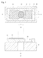
- Fig. 1 shows a piezoelectric thin-film resonator used in an experiment. More particularly, part (a) of Fig. 1 is a plan view of the resonator, and part (b) thereof is a cross-sectional view taken along a line A-A shown in part (a).
- a lower electrode 12 is formed on a silicon substrate 10, and is composed of two films of a Ru film and a Cr film.
- An upper electrode 16, which may, for example, be a Ru film, is provided on the piezoelectric film 14.
- An opening 20 is formed in the piezoelectric film 14 and is located above the lower electrode 12.
- the opening 20 is used to make an electrical connection with the lower electrode 12.
- a cavity 18 is formed in the silicon substrate 10 and is located below a portion in which the upper electrode 16 overlaps the lower electrode 12 across the piezoelectric film 14. Sputtering and etching may be used to form the lower electrode 13, the piezoelectric film 14 and the upper electrode 16.
- the cavity 18 may be defined by dry etching the silicon substrate 10 by deep-RIE so that the cavity 18 has a substantially vertical wall.
- the inventors prepared three piezoelectric thin-film resonators (resonators #1 through #3) each having a resonance frequency close to 2 GHz.
- the inventors investigated the relationships between the ratio of the major-axis length to the minor-axis length of an elliptical portion 22 in which the upper electrode 16 overlaps the lower electrode 12 across the piezoelectric film 14 and the spurious components in the resonance characteristics.
- the major and minor axes a and b of the elliptical portions 22 of resonators #1 through #3 had dimensions as shown in Table 1 in which the axial ratios are also shown.
- the elliptical portions 22 of resonators #1 through #3 had almost the same areas.
- Fig. 2A shows pass band characteristics of resonators #1 through #3
- Fig. 2B is an enlarged view of a rectangular portion shown in Fig. 2A. It can be seen from Fig. 2B that the different axial ratios a/b of the elliptical portion 22 change the frequencies at which spurious components occur. In a case where multiple resonators are combined to form a filter, if those resonators have identical frequencies at which spurious components occur, ripples take place in the pass band of the filter.
- a filter is made up of resonators having different frequencies at which spurious components occur, so that ripples in the pass band of the filter can be reduced.
- the first embodiment is a ladder type filter having a center frequency of 1950 MHz and including series-arm resonators and parallel-arm resonators.
- filters #1 through #3 we produced three samples of the above ladder type filter. These three samples are named filters #1 through #3.
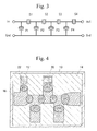
- Fig. 3 is a circuit diagram of filters #1 through #3.
- the ladder type filter of the first embodiment is composed of series-arm resonators S1 through S4 and parallel-arm resonators P1 through P4.
- Table 2 shows dimensions and ratios of the major and minor axes a and b of the elliptical portions 22 of the resonators of the produced ladder type filters (filters #1 through #3).
- Fig. 4 is a plan view of filter #1
- Fig. 5 is a plan view of filter #2
- Fig. 6 is a plan view of filter #3.
- identical numeral numbers are assigned to identical parts.
- filter #2 the series-arm resonators S1, S2 and S3 have different axial ratios of 1.8, 1.2 and 1.4 of the elliptical portions 22, respectively.
- the axial ratios of the series-arm resonator S4 and the parallel-arm resonators P1 through P4 are the same as those in filter #1.
- filter #2 is designed so that the elliptical portions 22 of the series-arm resonators S1 through S3 among the series-arm resonators S1 through S4 have almost the same areas but have different axial ratios.
- filter #3 the series-arm resonators S1 through S4 and the parallel-arm resonator P1 are the same as those of filter #2.
- the parallel-arm resonators P2, P3 and P4 have different axial ratios of 1.2, 1.4 and 1.6 of the elliptical portions 22, respectively.
- filter #3 is designed so that the elliptical portions 22 of the parallel-arm resonators P2 through P4 among the parallel-arm resonators P1 through P4 have almost the same areas but have different axial ratios.
- Figs. 7A through 7C show pass band characteristics of filters #1 through #3. Filters #1 through #3 have further reduced ripples in this order. This shows that the different axial ratios of the elliptical portions 22 of the multiple resonators change frequencies at which spurious components take place and ripples in the pas band can be restricted.
- the series-arm resonators and parallel-arm resonators that form the filter are not limited to those employed in the first embodiment.
- the present invention includes an arrangement in which the elliptical portion 22 of at least one of the series-arm and parallel-arm piezoelectric thin-film resonators has a shape different from the shapes of the elliptical portions 22 of the other resonators so that spurious components occur at different frequencies. It is thus possible to prevent spurious components of the piezoelectric thin-film resonators from overlapping and to suppress ripples in the pass band of the filter.
- the present invention is not limited to an arrangement in which all of the series-arm resonators and the parallel-arm resonators have elliptical portions, but includes another arrangement in which some resonators have overlapping portions 22 having a shape other than the ellipse. That is, only some resonators among the series-arm resonators and the parallel-arm resonators have the elliptical portions 22. At least one of the resonators having the elliptical portions 22 has an axial ratio a/b different from the axial ratios of the other resonators having the elliptical portions 22. It is thus possible to prevent spurious components of the multiple resonators having the elliptical portions 22 from overlapping and to reduce the ripples in the pass band of the filter, as shown in Figs. 7A through 7C.
- the resonators having different axial ratios a/b of the elliptical portions 22 may be assigned to the series-arm resonators S1 through S4.
- the series-arm resonators S1 through S4 are likely to have close frequencies at which spurious components occur.
- the different axial ratios of the elliptical portions 22 of the series-arm resonators S1 through S4 restrain ripples that occur in the pass band of the filter, as can be seen from the pass band characteristic of filter #1 (Fig. 7A) and that of filter #2 (Fig. 7B).
- the resonators having different axial ratios a/b of the elliptical portions 22 that have almost the same areas may be assigned to the series-arm resonators S2 through S4.
- the elliptical portions 22 having almost the same areas are designed to have the different axial ratios a/b in order to prevent the spurious components from overlapping and reduce the ripples in the bass band of the filter.
- all the series-arm resonators with the elliptical portions 22 having different areas are designed to have mutually different axial ratios a/b of the elliptical portions 22. This setting makes it possible to cause the spurious components in the series-arm resonators with the elliptical portions 22 having almost the same areas to be generated at mutually different frequencies and to further reduce the ripples in the pass band of the filter.
- the resonators having different axial ratios a/b of the elliptical portions 22 that have almost the same areas may be allotted to the parallel-arm resonators P1 through P4.
- the parallel-arm resonators are likely to have close frequencies at which spurious components occur.
- the different axial ratios of the elliptical portions 22 of the parallel-arm resonators P1 through P4 reduce the ripples in the pass band of the filter, as can be seen from comparison between the pass band of filter #1 (Fig. 7B) and that of filter #3 (Fig. 7C).
- the resonators having different axial ratios a/b of the elliptical portions 22 that have almost the same areas may be allotted to the parallel-arm resonators P2 through P4.
- the parallel-arm resonators with the elliptical portions 22 having almost the same areas can be given the mutually different frequencies at which spurious components occur, and the ripples in the pass band of the filter can be further reduced.
- the elliptical portions 22 of the series-arm resonators and the parallel-arm resonators have the mutually different axial ratios a/b.
- the resonators with the elliptical portions 22 having almost the same areas may be arbitrarily employed in accordance with the design specifications of the filter.
- the almost the same areas of the elliptical portions 22 of the resonators result in close frequencies at which spurious components overlap when the resonators are designed to have an identical axial ratio a/b.
- the close frequencies at which spurious components overlap are a factor that causes a ripple to occur in the pass band of the filter. For example, if the difference between the areas of the elliptical portions 22 of multiple resonators is equal to or less than ⁇ 20%, the multiple resonators will have close frequencies at which spurious components overlap. If the difference between the areas of the elliptical portions 22 of multiple resonators is equal to or less than ⁇ 10%, the multiple resonators will have closer frequencies at which spurious components overlap more greatly.
- the axial ratios a/b of the elliptical portions 22 of the resonators satisfy 1 ⁇ a/b ⁇ 1.9, as described in Japanese Patent Application Publication No. 2005-124107 . It is thus possible to reduce spurious components of the resonators and reduce ripples in the pass band of the filter.
- a second embodiment is a duplexer equipped with a transmit filter and a receive filter, which filters are configured in accordance with the above-mentioned first embodiment.
- a duplexer includes a transmit filter 32, a receive filter 34 and a matching circuit 31.
- the transmit filter 32 is provided between a common terminal 36 and a transmit terminal 38
- the receive filter 34 is provided between the common terminal 36 and a receive terminal 40. Since the transmit filter 32 and the receive filter 34 are configured in accordance with the first embodiment, the duplexer has reduced ripples in the pass bands.
- the first embodiment may be applied to both the transmit filter 32 and the receive filter 34 or one of these filters.
- the first and second embodiments use the piezoelectric thin-film resonators as shown in parts (a) and (b) of Figs. 1.
- These resonators may include the aforementioned silicon substrate 10, the lower electrode 12, the piezoelectric film 14 and the upper electrode 16, which may be formed with materials that have been described previously.
- the cavity 18 may be defined between the silicon substrate 10 and the lower electrode 12. That is, the lower electrode 12 has a curved portion in the elliptical portion 22 so as to be spaced apart from the silicon substrate 10.
- the resonators are not limited to FBAR but may be SMR.
- the structure shown in parts (a) and (b) of Fig. 1 is only a main portion of the resonator and another member may be applied thereto.
- a dielectric film serving as a reinforcement member or an etching stop layer for the cavity 18 may underlie the lower electrode 12 for frequency adjustment.
- a passivation film or a dielectric film for frequency adjustment may be provided on the upper electrode 16.
- the elliptical shape of the elliptical portion 22 is not limited to geometrically elliptical shapes but may include another shape, which may be obtained by deforming a circle symmetrical in the major and minor axes.
Landscapes
- Physics & Mathematics (AREA)
- Acoustics & Sound (AREA)
- Chemical & Material Sciences (AREA)
- Crystallography & Structural Chemistry (AREA)
- Piezo-Electric Or Mechanical Vibrators, Or Delay Or Filter Circuits (AREA)
Applications Claiming Priority (1)
| Application Number | Priority Date | Filing Date | Title |
|---|---|---|---|
| JP2006124447A JP4181185B2 (ja) | 2006-04-27 | 2006-04-27 | フィルタおよび分波器 |
Publications (3)
| Publication Number | Publication Date |
|---|---|
| EP1850479A2 true EP1850479A2 (de) | 2007-10-31 |
| EP1850479A3 EP1850479A3 (de) | 2008-07-30 |
| EP1850479B1 EP1850479B1 (de) | 2011-03-09 |
Family
ID=38267678
Family Applications (1)
| Application Number | Title | Priority Date | Filing Date |
|---|---|---|---|
| EP07106274A Active EP1850479B1 (de) | 2006-04-27 | 2007-04-16 | Filter und Duplexer |
Country Status (6)
| Country | Link |
|---|---|
| US (1) | US7786649B2 (de) |
| EP (1) | EP1850479B1 (de) |
| JP (1) | JP4181185B2 (de) |
| KR (1) | KR100863871B1 (de) |
| CN (1) | CN101064500B (de) |
| DE (1) | DE602007012955D1 (de) |
Families Citing this family (14)
| Publication number | Priority date | Publication date | Assignee | Title |
|---|---|---|---|---|
| JPWO2009066380A1 (ja) * | 2007-11-21 | 2011-03-31 | 太陽誘電株式会社 | フィルタ、それを用いたデュプレクサおよびそのデュプレクサを用いた通信機 |
| JP5322597B2 (ja) * | 2008-11-13 | 2013-10-23 | 太陽誘電株式会社 | 共振子、フィルタ、デュープレクサおよび電子装置 |
| JP5394847B2 (ja) * | 2009-08-06 | 2014-01-22 | 太陽誘電株式会社 | 分波器 |
| JP2011041136A (ja) * | 2009-08-17 | 2011-02-24 | Taiyo Yuden Co Ltd | 弾性波デバイスおよびその製造方法 |
| JP5360432B2 (ja) * | 2011-01-27 | 2013-12-04 | 株式会社村田製作所 | 圧電デバイス |
| JP5613813B2 (ja) * | 2013-10-17 | 2014-10-29 | 太陽誘電株式会社 | 分波器 |
| KR20200028034A (ko) * | 2017-08-03 | 2020-03-13 | 어쿠스티스, 인크. | 벌크 음향파 공진기에 대한 타원형 구조체 |
| US10727811B2 (en) * | 2018-06-01 | 2020-07-28 | Akoustis, Inc. | Effective coupling coefficients for strained single crystal epitaxial film bulk acoustic resonators |
| US11211918B2 (en) | 2018-06-01 | 2021-12-28 | Akoustis, Inc. | Effective coupling coefficients for strained single crystal epitaxial film bulk acoustic resonators |
| US11552613B2 (en) | 2019-04-19 | 2023-01-10 | Akoustis, Inc. | Resonator shapes for bulk acoustic wave (BAW) devices |
| US20200357849A1 (en) * | 2019-05-07 | 2020-11-12 | Fox Enterprises, Inc. | Monolithic composite resonator devices with intrinsic mode control |
| KR102789019B1 (ko) * | 2019-07-31 | 2025-03-31 | 삼성전기주식회사 | 체적 음향 공진기 |
| US20230318570A1 (en) * | 2022-03-30 | 2023-10-05 | Skyworks Solutions, Inc. | Bulk acoustic wave devices with suppressed nonlinear response |
| WO2025211121A1 (ja) * | 2024-04-01 | 2025-10-09 | 株式会社村田製作所 | 弾性波フィルタ、マルチプレクサ、高周波フロントエンド回路及び通信装置 |
Citations (2)
| Publication number | Priority date | Publication date | Assignee | Title |
|---|---|---|---|---|
| JP2003133892A (ja) | 2001-10-29 | 2003-05-09 | Tdk Corp | 圧電薄膜振動素子、及びこれを用いたフィルタ |
| US20050099094A1 (en) | 2003-10-20 | 2005-05-12 | Tokihiro Nishihara | Piezoelectric thin-film resonator and filter using the same |
Family Cites Families (8)
| Publication number | Priority date | Publication date | Assignee | Title |
|---|---|---|---|---|
| JPH0513061Y2 (de) * | 1987-07-27 | 1993-04-06 | ||
| SE0001926D0 (sv) * | 2000-05-23 | 2000-05-23 | Lars Liljeryd | Improved spectral translation/folding in the subband domain |
| JP3969224B2 (ja) | 2002-01-08 | 2007-09-05 | 株式会社村田製作所 | 圧電共振子及びそれを用いた圧電フィルタ・デュプレクサ・通信装置 |
| JP3988864B2 (ja) * | 2002-03-26 | 2007-10-10 | Tdk株式会社 | フィルタ及びこれを用いた分波器 |
| ATE373892T1 (de) * | 2003-12-22 | 2007-10-15 | Infineon Technologies Ag | Dünnfilmresonator-abzweigfilter und verfahren zur erdung dieser filter |
| JP4223428B2 (ja) | 2004-03-31 | 2009-02-12 | 富士通メディアデバイス株式会社 | フィルタおよびその製造方法 |
| US7187255B2 (en) * | 2004-10-26 | 2007-03-06 | Avago Technologies Wireless Ip (Singapore) Pte. Ltd. | Arrangement of lattice filter |
| JP5128077B2 (ja) | 2006-02-21 | 2013-01-23 | 宇部興産株式会社 | 薄膜圧電共振器とそれを用いた薄膜圧電フィルタ |
-
2006
- 2006-04-27 JP JP2006124447A patent/JP4181185B2/ja not_active Expired - Lifetime
-
2007
- 2007-04-16 DE DE602007012955T patent/DE602007012955D1/de active Active
- 2007-04-16 EP EP07106274A patent/EP1850479B1/de active Active
- 2007-04-25 KR KR1020070040435A patent/KR100863871B1/ko active Active
- 2007-04-26 US US11/790,530 patent/US7786649B2/en active Active
- 2007-04-27 CN CN2007101077015A patent/CN101064500B/zh active Active
Patent Citations (2)
| Publication number | Priority date | Publication date | Assignee | Title |
|---|---|---|---|---|
| JP2003133892A (ja) | 2001-10-29 | 2003-05-09 | Tdk Corp | 圧電薄膜振動素子、及びこれを用いたフィルタ |
| US20050099094A1 (en) | 2003-10-20 | 2005-05-12 | Tokihiro Nishihara | Piezoelectric thin-film resonator and filter using the same |
Also Published As
| Publication number | Publication date |
|---|---|
| JP2007300216A (ja) | 2007-11-15 |
| EP1850479B1 (de) | 2011-03-09 |
| EP1850479A3 (de) | 2008-07-30 |
| JP4181185B2 (ja) | 2008-11-12 |
| KR20070105881A (ko) | 2007-10-31 |
| CN101064500B (zh) | 2010-06-23 |
| CN101064500A (zh) | 2007-10-31 |
| US20070252662A1 (en) | 2007-11-01 |
| US7786649B2 (en) | 2010-08-31 |
| KR100863871B1 (ko) | 2008-10-15 |
| DE602007012955D1 (de) | 2011-04-21 |
Similar Documents
| Publication | Publication Date | Title |
|---|---|---|
| EP1850479B1 (de) | Filter und Duplexer | |
| US7298230B2 (en) | Duplexer utilizing a compact splitter circuit | |
| KR100625701B1 (ko) | 필터 소자, 그것을 구비한 필터 장치, 분파기 및 고주파회로 | |
| US10666220B2 (en) | Acoustic wave device | |
| US9071224B2 (en) | Filter and duplexer | |
| CN101674062B (zh) | 滤波器、双工器和通信装置 | |
| EP1755216A2 (de) | Piezoelektrischer Resonator, piezoelektrischer Filter und Kommunikationsvorrichtung | |
| US20040150293A1 (en) | Component operating with bulk acoustic waves, and having asymmetric/symmetrical circuitry | |
| EP1914888A1 (de) | Abzweigfilter | |
| US8164398B2 (en) | Resonator, filter and electronic device | |
| CN111010120A (zh) | 具有调节层的体声波谐振器、滤波器和电子设备 | |
| US20180175275A1 (en) | Piezoelectric thin film resonator, filter, and multiplexer | |
| JP2006510296A (ja) | 電気音響共振器 | |
| US12255604B2 (en) | Acoustic wave device and filter | |
| US10554196B2 (en) | Acoustic wave device | |
| JP2018101964A (ja) | 弾性波デバイス | |
| JP2024140687A (ja) | 弾性波デバイス、フィルタ、およびマルチプレクサ | |
| JP2020198569A (ja) | 圧電薄膜共振器、フィルタおよびマルチプレクサ | |
| JP2019212982A (ja) | 圧電薄膜共振器、フィルタおよびマルチプレクサ | |
| US12255602B2 (en) | Filter and multiplexer | |
| JP2019121874A (ja) | フィルタおよびマルチプレクサ | |
| WO2025211079A1 (ja) | 弾性波共振子、弾性波フィルタ、マルチプレクサ、高周波フロントエンド回路及び通信装置 | |
| WO2025211077A1 (ja) | 弾性波共振子、弾性波フィルタ、マルチプレクサ、高周波フロントエンド回路及び通信装置 | |
| JP2018182455A (ja) | 弾性波フィルタおよびマルチプレクサ | |
| WO2025211121A1 (ja) | 弾性波フィルタ、マルチプレクサ、高周波フロントエンド回路及び通信装置 |
Legal Events
| Date | Code | Title | Description |
|---|---|---|---|
| PUAI | Public reference made under article 153(3) epc to a published international application that has entered the european phase |
Free format text: ORIGINAL CODE: 0009012 |
|
| AK | Designated contracting states |
Kind code of ref document: A2 Designated state(s): AT BE BG CH CY CZ DE DK EE ES FI FR GB GR HU IE IS IT LI LT LU LV MC MT NL PL PT RO SE SI SK TR |
|
| AX | Request for extension of the european patent |
Extension state: AL BA HR MK YU |
|
| PUAL | Search report despatched |
Free format text: ORIGINAL CODE: 0009013 |
|
| AK | Designated contracting states |
Kind code of ref document: A3 Designated state(s): AT BE BG CH CY CZ DE DK EE ES FI FR GB GR HU IE IS IT LI LT LU LV MC MT NL PL PT RO SE SI SK TR |
|
| AX | Request for extension of the european patent |
Extension state: AL BA HR MK RS |
|
| 17P | Request for examination filed |
Effective date: 20090126 |
|
| AKX | Designation fees paid |
Designated state(s): DE FR GB |
|
| 17Q | First examination report despatched |
Effective date: 20091105 |
|
| RAP1 | Party data changed (applicant data changed or rights of an application transferred) |
Owner name: FUJITSU MEDIA DEVICES LIMITED Owner name: TAIYO YUDEN CO., LTD. |
|
| GRAP | Despatch of communication of intention to grant a patent |
Free format text: ORIGINAL CODE: EPIDOSNIGR1 |
|
| RAP1 | Party data changed (applicant data changed or rights of an application transferred) |
Owner name: TAIYO YUDEN CO., LTD. |
|
| GRAS | Grant fee paid |
Free format text: ORIGINAL CODE: EPIDOSNIGR3 |
|
| GRAA | (expected) grant |
Free format text: ORIGINAL CODE: 0009210 |
|
| AK | Designated contracting states |
Kind code of ref document: B1 Designated state(s): DE FR GB |
|
| REG | Reference to a national code |
Ref country code: GB Ref legal event code: FG4D |
|
| REF | Corresponds to: |
Ref document number: 602007012955 Country of ref document: DE Date of ref document: 20110421 Kind code of ref document: P |
|
| REG | Reference to a national code |
Ref country code: DE Ref legal event code: R096 Ref document number: 602007012955 Country of ref document: DE Effective date: 20110421 |
|
| PLBE | No opposition filed within time limit |
Free format text: ORIGINAL CODE: 0009261 |
|
| STAA | Information on the status of an ep patent application or granted ep patent |
Free format text: STATUS: NO OPPOSITION FILED WITHIN TIME LIMIT |
|
| 26N | No opposition filed |
Effective date: 20111212 |
|
| REG | Reference to a national code |
Ref country code: DE Ref legal event code: R097 Ref document number: 602007012955 Country of ref document: DE Effective date: 20111212 |
|
| PGFP | Annual fee paid to national office [announced via postgrant information from national office to epo] |
Ref country code: GB Payment date: 20140422 Year of fee payment: 8 |
|
| PGFP | Annual fee paid to national office [announced via postgrant information from national office to epo] |
Ref country code: FR Payment date: 20140422 Year of fee payment: 8 |
|
| GBPC | Gb: european patent ceased through non-payment of renewal fee |
Effective date: 20150416 |
|
| PG25 | Lapsed in a contracting state [announced via postgrant information from national office to epo] |
Ref country code: GB Free format text: LAPSE BECAUSE OF NON-PAYMENT OF DUE FEES Effective date: 20150416 |
|
| REG | Reference to a national code |
Ref country code: FR Ref legal event code: ST Effective date: 20151231 |
|
| PG25 | Lapsed in a contracting state [announced via postgrant information from national office to epo] |
Ref country code: FR Free format text: LAPSE BECAUSE OF NON-PAYMENT OF DUE FEES Effective date: 20150430 |
|
| P01 | Opt-out of the competence of the unified patent court (upc) registered |
Effective date: 20230509 |
|
| PGFP | Annual fee paid to national office [announced via postgrant information from national office to epo] |
Ref country code: DE Payment date: 20250305 Year of fee payment: 19 |