EP1847979A2 - Verfahren und Vorrichtung zur Betätigung eines Bildschirms, insbesondere eines Plasmabildschirms, und entsprechende Vorrichtung - Google Patents
Verfahren und Vorrichtung zur Betätigung eines Bildschirms, insbesondere eines Plasmabildschirms, und entsprechende Vorrichtung Download PDFInfo
- Publication number
- EP1847979A2 EP1847979A2 EP07106240A EP07106240A EP1847979A2 EP 1847979 A2 EP1847979 A2 EP 1847979A2 EP 07106240 A EP07106240 A EP 07106240A EP 07106240 A EP07106240 A EP 07106240A EP 1847979 A2 EP1847979 A2 EP 1847979A2
- Authority
- EP
- European Patent Office
- Prior art keywords
- column
- selection mode
- screen
- selection
- state
- Prior art date
- Legal status (The legal status is an assumption and is not a legal conclusion. Google has not performed a legal analysis and makes no representation as to the accuracy of the status listed.)
- Withdrawn
Links
Images


Classifications
-
- G—PHYSICS
- G09—EDUCATION; CRYPTOGRAPHY; DISPLAY; ADVERTISING; SEALS
- G09G—ARRANGEMENTS OR CIRCUITS FOR CONTROL OF INDICATING DEVICES USING STATIC MEANS TO PRESENT VARIABLE INFORMATION
- G09G3/00—Control arrangements or circuits, of interest only in connection with visual indicators other than cathode-ray tubes
- G09G3/20—Control arrangements or circuits, of interest only in connection with visual indicators other than cathode-ray tubes for presentation of an assembly of a number of characters, e.g. a page, by composing the assembly by combination of individual elements arranged in a matrix no fixed position being assigned to or needed to be assigned to the individual characters or partial characters
- G09G3/22—Control arrangements or circuits, of interest only in connection with visual indicators other than cathode-ray tubes for presentation of an assembly of a number of characters, e.g. a page, by composing the assembly by combination of individual elements arranged in a matrix no fixed position being assigned to or needed to be assigned to the individual characters or partial characters using controlled light sources
- G09G3/28—Control arrangements or circuits, of interest only in connection with visual indicators other than cathode-ray tubes for presentation of an assembly of a number of characters, e.g. a page, by composing the assembly by combination of individual elements arranged in a matrix no fixed position being assigned to or needed to be assigned to the individual characters or partial characters using controlled light sources using luminous gas-discharge panels, e.g. plasma panels
- G09G3/288—Control arrangements or circuits, of interest only in connection with visual indicators other than cathode-ray tubes for presentation of an assembly of a number of characters, e.g. a page, by composing the assembly by combination of individual elements arranged in a matrix no fixed position being assigned to or needed to be assigned to the individual characters or partial characters using controlled light sources using luminous gas-discharge panels, e.g. plasma panels using AC panels
- G09G3/296—Driving circuits for producing the waveforms applied to the driving electrodes
-
- G—PHYSICS
- G09—EDUCATION; CRYPTOGRAPHY; DISPLAY; ADVERTISING; SEALS
- G09G—ARRANGEMENTS OR CIRCUITS FOR CONTROL OF INDICATING DEVICES USING STATIC MEANS TO PRESENT VARIABLE INFORMATION
- G09G3/00—Control arrangements or circuits, of interest only in connection with visual indicators other than cathode-ray tubes
- G09G3/20—Control arrangements or circuits, of interest only in connection with visual indicators other than cathode-ray tubes for presentation of an assembly of a number of characters, e.g. a page, by composing the assembly by combination of individual elements arranged in a matrix no fixed position being assigned to or needed to be assigned to the individual characters or partial characters
- G09G3/22—Control arrangements or circuits, of interest only in connection with visual indicators other than cathode-ray tubes for presentation of an assembly of a number of characters, e.g. a page, by composing the assembly by combination of individual elements arranged in a matrix no fixed position being assigned to or needed to be assigned to the individual characters or partial characters using controlled light sources
- G09G3/28—Control arrangements or circuits, of interest only in connection with visual indicators other than cathode-ray tubes for presentation of an assembly of a number of characters, e.g. a page, by composing the assembly by combination of individual elements arranged in a matrix no fixed position being assigned to or needed to be assigned to the individual characters or partial characters using controlled light sources using luminous gas-discharge panels, e.g. plasma panels
- G09G3/288—Control arrangements or circuits, of interest only in connection with visual indicators other than cathode-ray tubes for presentation of an assembly of a number of characters, e.g. a page, by composing the assembly by combination of individual elements arranged in a matrix no fixed position being assigned to or needed to be assigned to the individual characters or partial characters using controlled light sources using luminous gas-discharge panels, e.g. plasma panels using AC panels
- G09G3/291—Control arrangements or circuits, of interest only in connection with visual indicators other than cathode-ray tubes for presentation of an assembly of a number of characters, e.g. a page, by composing the assembly by combination of individual elements arranged in a matrix no fixed position being assigned to or needed to be assigned to the individual characters or partial characters using controlled light sources using luminous gas-discharge panels, e.g. plasma panels using AC panels controlling the gas discharge to control a cell condition, e.g. by means of specific pulse shapes
- G09G3/293—Control arrangements or circuits, of interest only in connection with visual indicators other than cathode-ray tubes for presentation of an assembly of a number of characters, e.g. a page, by composing the assembly by combination of individual elements arranged in a matrix no fixed position being assigned to or needed to be assigned to the individual characters or partial characters using controlled light sources using luminous gas-discharge panels, e.g. plasma panels using AC panels controlling the gas discharge to control a cell condition, e.g. by means of specific pulse shapes for address discharge
-
- G—PHYSICS
- G09—EDUCATION; CRYPTOGRAPHY; DISPLAY; ADVERTISING; SEALS
- G09G—ARRANGEMENTS OR CIRCUITS FOR CONTROL OF INDICATING DEVICES USING STATIC MEANS TO PRESENT VARIABLE INFORMATION
- G09G2330/00—Aspects of power supply; Aspects of display protection and defect management
- G09G2330/02—Details of power systems and of start or stop of display operation
- G09G2330/021—Power management, e.g. power saving
- G09G2330/023—Power management, e.g. power saving using energy recovery or conservation
Definitions
- the invention relates to plasma screens, and more particularly the control of the cells of such a screen.
- a plasma screen is a matrix type screen, formed of cells arranged at the interconnections of lines and columns.
- a cell comprises a cavity filled with a rare gas, and at least two control electrodes.
- To create a luminous point on the screen using a given cell the cell is selected by applying a potential difference between its control electrodes, and then an ionisation of the gas of the cell is generally initiated by means of a third electrode. ordered. This ionization is accompanied by an emission of ultraviolet rays.
- the creation of the luminous point is obtained by excitation of a red, green or blue luminescent material by the emitted rays.
- control of a plasma screen essentially comprises two phases, namely an addressing phase in which the cells (pixels) which are to be switched on and those which are to be extinguished, and a display phase are determined. itself in which the cells that have been selected in the addressing phase are actually turned on.
- the addressing phase comprises a sequential selection of the rows of the matrix, generally a successive selection of the even lines followed by a successive selection of the odd lines.
- the non-selected lines are set at a rest potential, for example 150 volts, while a selected line is brought to an activation potential, for example 0 volts.
- the pixels that in the display phase the corresponding columns of the matrix are for example brought to a relatively high potential, for example 70 volts, via a power stage comprising MOS power transistors.
- Columns corresponding to the other pixels of the selected line, which should not be lit, are brought to potential 0 volts.
- the cells of the activated line which will have to be lit, see a potential column-line equal to about 70 volts while the other cells of this line see a potential column-line equal to 0 volts.
- the selection and deselection of the columns of the screen are made using a selection and deselection signal, according to a mode known as the "Charge Sharing Effect” (CSE), in English ).
- CSE Charge Sharing Effect
- part of the necessary charges come from a capacitor incorporated in the control circuit of the screen.
- the output of the column control circuit is first coupled to the charge capacitor so as to load it by restoring a portion of the charges.
- the deselection signal therefore passes from its maximum value to the intermediate stage value, then the column control circuit output coupled to the column in question is switched to the circuit ground, so that the deselection signal reaches its minimum value. .
- the CSE mode reduces the energy consumption of the circuit since some of the charges come from a capacitor.
- the energy gain can reach up to 50% compared to a circuit operating without this mode.
- the invention aims to provide a solution to this problem.
- An object of the invention is to eliminate the appearance of black pixels on the screen, especially at the beginning of the screen scan, while maintaining the CSE mode, to save energy used.
- a method of controlling a matrix screen comprising successive sweeps of the screen, each scan of the screen comprising a successive selection of lines of the screen, and for each selected line, a first column selection mode in which each column to be selected is selected with a first selection signal passing from a first state to a second state with a intermediate level.
- this first aspect of the invention there is further provided a second column selection mode in which each column to be selected is selected with a second selection signal passing from the first state to the second state without intermediate stage At least at the beginning of each scan, the first selection mode is replaced by the second selection mode, and this second selection mode is retained for a given column, at the latest, as long as no deselection of said column has been performed .
- the first selection mode (in other words the CSE mode in the case of the selection of a column) of a column to be selected is suppressed, as long as this column has not been deselected.
- the inventors have observed that the black pixels systematically appear at the beginning of the screen scan, when a pixel belonging to a previously unselected column was selected.
- the selection signal is subjected to the CSE mode, with the generation of the signal in two stages.
- the CSE mode has no influence
- the inventors deduced that the problem was related to the CSE mode and more particularly to the transfer of the charges from the storage means to the outputs of the control block of columns. Indeed, by observing the selection signals for different lines of the screen, the inventors have noticed that the portion of the signal due to the transfer of charges from the storage means to the output did not go from its minimum value to the value of the bearing. intermediate.
- the selection signal was then triggered only when the output of the column control block was switched to the power terminal of the circuit. This delay then caused a disturbance of the data transmitted at the same time to the column control block for the addressing of the next line.
- the absence of charge transfer between the storage means and the output of the column control block reflects the insufficient charge within the storage means at the time of generation of the selection signal.
- the inventors have justified this situation that before each start of a scan of the screen, the validation signal of the addressing phase is returned to the low state forcing the coupling of the outputs of the column control block to the mass.
- the storage capacitor is not sufficiently charged to ensure a transfer of loads to the outputs of the control block of the columns to be selected.
- the invention allowing at least at the beginning of each scan, to select the columns without involving the means storage during the selection of columns, is freed from the fact that the storage means can be unloaded at this time.
- the scanning of the screen comprises an addressing phase associated with a validation signal.
- the addressing phase for each selected line, the columns to be selected and the columns to be deselected are determined, said addressing phase being performed when the validation signal is in an active state.
- the first selection mode can be replaced by the second selection mode, also when said enable signal of the addressing phase goes into the active state.
- the screen comprises n columns coupled to a charge storage means. It is preferable to retain the second selection mode until it is detected that the quantity of charges stored by the storage means has reached said given threshold.
- the quantity of charges of a storage means is determined, and this quantity is sufficient, the first mode of selection is restored.
- the storage means comprises for example a storage capacitor, at the terminals of which the voltage is measured. It is considered that the quantity of charges stored has reached said threshold when the measured voltage has reached a chosen value.
- the quantity of stored charges is considered to have reached said threshold when n column deselections have been accounted for.
- a device for controlling a matrix screen comprising means with a row control block capable of successively selecting each line, and a column control block suitable for each selected line, to select a set of deselected columns, said column control block being suitable for each selected line to selecting, in a first selection mode, each column to be selected with a first selection signal passing from a first state to a second state with an intermediate stage.
- the column control block is furthermore capable of operating according to a second column selection mode in which the column control block is capable of selecting each column to be selected with a second signal from the column. selection passing from the first state to the second state without intermediate stage.
- Said column control block is adapted at least at the beginning of each scan, to replace the first selection mode by the second selection mode, and to keep the second selection mode for a given column, at the latest, as long as said column has not been deselected.
- the scanning means comprise addressing means associated with a validation signal, able to determine for each selected line, the columns to be selected and the columns to be deselected, when the validation signal is in a state. active.
- Said column control block is also able to replace for each column to be selected, the first selection mode by the second selection mode, when said enable signal of the addressing means goes to the active state.
- the screen comprises n columns coupled to a charge storage means.
- the device can furthermore comprise means for detecting the quantity of charges stored by the storage means, the column control block being able to keep the second selection mode until the detection means detect that the quantity of charges stored by the storage means has reached said given threshold.
- the storage means comprises for example a storage capacitor.
- Said detection means then comprise measuring means able to measure the voltage at the terminals of the storage capacitor, said given threshold corresponding to a chosen value of the voltage measured at the terminals of the storage capacitor.
- the device may furthermore comprise storage means adapted during the first selection mode, to memorize a variable taking a first value as soon as the control block replaces the first selection mode with the second selection mode, and a second value if not.
- the device may furthermore comprise, for each column, initialization means receiving said input variable and delivering a secondary variable, taking the second value as soon as the column in question is deselected.
- the deselection of the columns can then be carried out conventionally, which makes it possible to recharge the storage means, and to restore the first selection mode for the next selection of the column considered.
- a screen system in particular a matrix plasma screen, incorporating a control device as described above.
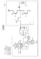
- FIG. 1 very schematically represents a structure of a matrix plasma screen ECR formed of a cell CELij (corresponding to pixels of the image).
- Each cell CELij has two control electrodes respectively connected to a line Li and to a column Cj, j varying from 0 to n (where n is the number of columns of the screen).
- Each cell has an equivalent capacity of the order of several tens of pF.
- the control device of this screen comprises a line control circuit capable of sequentially selecting the rows of the matrix (not shown), and a column control circuit BCC able to select and possibly deselect several previously selected columns.
- circuits are generally integrated on a semiconductor chip.
- Vpp typically of the order of 70 volts (to turn on or off a pixel according to the embodiment chosen for the screen).
- the column control block BCC conventionally comprises three transistors SWH, SWL and SWM, respectively, controlled by control means MCOM.
- the transistor SWH may for example be an NMOS type transistor.
- the transistor SWH can connect the output Sj to the supply voltage Vpp.
- This output Sj is the output of the column control block BCC which is connected to the column Cj comprising the cells CELj (each cell CELj comprising a capacitor Ccolj).
- the transistor SWL makes it possible to connect the output Sj to the GND circuit ground.
- the transistor SWL can be realized for example by means of a PMOS transistor.
- the control means can be implemented within the BCC column control block in the form of an integrated circuit, or upstream of it.
- control means MCOM can be implemented using a software tool.
- the screen also includes a storage capacitor Cst (preferably external to the BCC column control block), coupled between the mass and all the columns of the screen.
- Cst preferably external to the BCC column control block
- the capacitor Cst is connected to the output Sj, via the transistor SWM.
- the storage capacitor Cst may be a specific capacitor added to the circuit, its capacitive value preferably being equal to the sum of the capacitive values of the capacitors Ccolj. But the storage capacitor can also be formed by all the capacitors already present in each component of the circuit.
- the transistor SWM may for example be a PMOS type transistor, associated with a DSWM diode connected between its source and its drain.
- the voltage V EC is measured at the terminals of the storage capacitor Cst using measurement means MMES, for example a comparator.
- MMES measurement means
- the value of this voltage V EC varies between zero and a value between zero and Vpp, preferably Vpp / 2.
- a counter of the column deselection number could be provided, the counting of n deselections ensuring that the capacitor Cst is charged, ie V EC ⁇ Vpp / 2.
- the control means MCOM receives as input the value of the voltage V EC measured at the terminals of the storage capacitor Cst, and of signals prepared by external means MEXT, respectively STB, CSE and BLK.
- the signal STB (Strobe" in English) makes it possible to elaborate the control signal of the transistor SWM, as will be seen hereinafter.
- the CSE signal indicates that the selection and deselection of the columns is done according to the CSE mode.
- the signal BLK corresponds to the validation signal of the addressing phase.
- control means MCOM are coupled to a shift register SR, which receives as input the data DATA to be delivered on each column Cj, during the addressing phase.
- the register SR is clocked by a clock signal CK, generated for example by a quartz clock QZ.
- the output of the register SR is connected to a first flip-flop D1, for example a flip-flop D, controlled by the signal STB.
- the register SR delivers the data qj, i for the column Cj and the line Li, to the flip-flop D1.
- the register SR delivers the data for the column Cj and the line Li + 1 to the flip-flop D1, which in turn sends its data qj, i to a second flip-flop D2 (for example a flip-flop D).
- the flip-flops D1 and D2 respectively deliver the data qj, i and qj, i + 1 to the control means MCOM, at each edge of the signal STB.
- the means MCOM then address each line Li + 1, at each falling edge, for example, of the signal STB with the data qj, i + 1.
- the means MCOM determine the changes of state of a column Cj, by comparing the data qj, i and qj, i + 1, as will be seen below.
- the control means MCOM incorporate means for controlling the mode CSE, MCSE, adapted from the signal STB, the mode signal CSE, the signal BLK and data qj, i and qj, i + 1, to be elaborated an internal signal CSE mode for each column Cj, this internal signal (explained in more detail below) being referenced CSEj.
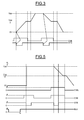
- FIG. 3 illustrates the variations of the selection signal of a column Cj, in the addressing phase and during the CSE mode, according to a first conventional selection mode.
- a new falling edge of the signal STB causes the discharge of the capacitor Ccolj to the storage capacitor Cst as long as the value of the deselection signal at the output Sj is between Vpp and Vpp / 2 (the transistor SWM is "on", and the SWL and SWH transistors "blocked").
- control means cause the switching of the output Sj GND ground, (the SWL transistor is "passing” and transistors SWH and SWM “blocked”).
- a second selection mode can replace the first mode mentioned above, when the storage capacitor is discharged, as explained above.
- the MCSE means (shown in FIG. 4) comprise means MCOND capable of detecting whether the conditions making it possible to pass to the second selection mode are fulfilled.
- These means MCOND receive as input the signal CSE and the validation signal of the addressing phase BLK.
- the means MCOND If the means MCOND have recorded a rising edge of the signal BLK ( ⁇ BLK), indicating the validation of the addressing phase, the means MCOND require the passage to the second selection mode.
- the scan comprises two subscans, for example a subsampling of the even lines followed by a subscanning of the odd lines, an edge of the signal BLK occurs at the start of each sub-scan.
- V EC voltage EC
- Vthreshold threshold voltage
- the MSCE means comprise memory means MM capable of storing a Flag variable taking the value "0" if the first selection mode is to be applied, and "1", if the first selection mode is replaced by the second selection mode.
- This Flag variable is delivered to means MEij of the signal CSEj.
- Each means of elaboration MELj comprises means of initialization MRZ of the variable Flag and deliver a secondary variable Flag2 elaborated from the variable Flag.
- the initialization means MRZ are controlled by means for detecting a falling edge MFD.
- the means MFD input the data qj, i + 1 and qj, i, so as to detect the occurrence of a falling edge for a column Cj, between two successive selections of lines, Li and Li + 1.
- the Flag2 variable initially takes the value of the Flag variable. Therefore, if the second selection mode is applied, Flag2 is equal to 1.
- the means MFD deliver a signal to the reset means MRZ so as to set the Flag variable to zero for the column Cj.
- the signal CSj allows the transfer of the charge of the column capacitor Ccolj to the storage capacitor Cst to recharge the latter.
- the production means MELj finally comprise a processing block BELj receiving as input the flag variable and the signal CSE so as to develop the signal CSEj as described in FIG.
- the MCOND means can also memorize a synchronization condition ( BLK & CSE ) so as not to trigger the rise of the selection signal until the black screen signal has taken the value "1".
- FIG. 5 illustrates the variation of the selection signal at the output Sj, in the case where the second selection mode replaces the first selection mode.
- the signal BLK goes from "0" to "1".
- the BCC control block replaces the first selection mode with the second (it is assumed that V CE ⁇ Vthreshold).
- the CSj signal also returns to the value "1", so as to return to the conventional operating mode.
- the selection signal goes from Vpp to Vpp / 2 (involving the charge of the storage capacitor Cst) and then, after an additional step, from the value Vpp / 2 to zero volts.
Landscapes
- Engineering & Computer Science (AREA)
- Physics & Mathematics (AREA)
- Power Engineering (AREA)
- Plasma & Fusion (AREA)
- Computer Hardware Design (AREA)
- General Physics & Mathematics (AREA)
- Theoretical Computer Science (AREA)
- Control Of Indicators Other Than Cathode Ray Tubes (AREA)
Applications Claiming Priority (1)
| Application Number | Priority Date | Filing Date | Title |
|---|---|---|---|
| FR0603445A FR2900266A1 (fr) | 2006-04-19 | 2006-04-19 | Procede de commande d'un ecran, en particulier d'un ecran a plasma, et dispositif correspondant |
Publications (2)
| Publication Number | Publication Date |
|---|---|
| EP1847979A2 true EP1847979A2 (de) | 2007-10-24 |
| EP1847979A3 EP1847979A3 (de) | 2009-09-23 |
Family
ID=37529364
Family Applications (1)
| Application Number | Title | Priority Date | Filing Date |
|---|---|---|---|
| EP07106240A Withdrawn EP1847979A3 (de) | 2006-04-19 | 2007-04-16 | Verfahren und Vorrichtung zur Betätigung eines Bildschirms, insbesondere eines Plasmabildschirms, und entsprechende Vorrichtung |
Country Status (3)
| Country | Link |
|---|---|
| US (2) | US7961203B2 (de) |
| EP (1) | EP1847979A3 (de) |
| FR (1) | FR2900266A1 (de) |
Family Cites Families (6)
| Publication number | Priority date | Publication date | Assignee | Title |
|---|---|---|---|---|
| US4316123A (en) * | 1980-01-08 | 1982-02-16 | International Business Machines Corporation | Staggered sustain voltage generator and technique |
| JP3447185B2 (ja) * | 1996-10-15 | 2003-09-16 | 富士通株式会社 | フラット表示パネルを利用した表示装置 |
| JPH1185093A (ja) * | 1997-09-02 | 1999-03-30 | Pioneer Electron Corp | 表示パネル駆動装置 |
| FR2812963B1 (fr) * | 2000-08-11 | 2003-07-25 | St Microelectronics Sa | Procede et circuit de commande de cellules d'un ecran a plasma |
| JP2002175043A (ja) * | 2000-12-06 | 2002-06-21 | Nec Corp | プラズマディスプレイパネルの駆動方法、その回路及び表示装置 |
| JP2005043682A (ja) * | 2003-07-22 | 2005-02-17 | Nec Plasma Display Corp | プラズマ表示装置及びその駆動方法 |
-
2006
- 2006-04-19 FR FR0603445A patent/FR2900266A1/fr active Pending
-
2007
- 2007-04-16 EP EP07106240A patent/EP1847979A3/de not_active Withdrawn
- 2007-04-18 US US11/788,031 patent/US7961203B2/en not_active Expired - Fee Related
-
2011
- 2011-03-31 US US13/076,703 patent/US20110175887A1/en not_active Abandoned
Also Published As
| Publication number | Publication date |
|---|---|
| FR2900266A1 (fr) | 2007-10-26 |
| EP1847979A3 (de) | 2009-09-23 |
| US7961203B2 (en) | 2011-06-14 |
| US20110175887A1 (en) | 2011-07-21 |
| US20070252781A1 (en) | 2007-11-01 |
Similar Documents
| Publication | Publication Date | Title |
|---|---|---|
| EP2503775B1 (de) | Zweitakt-Bilderfassungsgerät mit Integration und konditioneller Auswahl | |
| CA2692300C (fr) | Procede et systeme de gestion de coupures d'alimentation electrique a bord d'un aeronef | |
| FR2858725A1 (fr) | Dispositif autoreparable pour generer une haute tension, et procede de reparation d'un dispositif pour generer une haute tension. | |
| FR2501891A1 (fr) | Memoire semi-conductrice autocorrectrice d'erreurs | |
| FR2943199A1 (fr) | Procede de lecture de signal de capteur d'image et capteur d'image. | |
| FR2934919A1 (fr) | Registre a decalage a transistors a effet de champ. | |
| FR2973162A1 (fr) | Capteur d'image a tres haute dynamique | |
| FR2744276A1 (fr) | Dispositif d'affichage a panneau d'affichage par plasma, son procede d'excitation, et un generateur d'onde utilise avec celui-ci | |
| FR2772502A1 (fr) | Procede de compensation des differences de remanence des luminophores dans un ecran de visualisation d'images | |
| EP3496101A1 (de) | Sram-speicher mit schneller löschfunktion | |
| WO2008034677A1 (fr) | Capteur d'image lineaire cmos a fonctionnement de type transfert de charges | |
| EP2073212B1 (de) | Lesevorrichtung eines nichtflüchtigen Speichers mit geringem Energieverbrauch und ihr Anwendungsverfahren | |
| EP0965224B1 (de) | Verfahren zur steuerung einer lichtempfindlichen vorrichtung mit schwacher remanenz und lichtempfindliche vorrichtung zur durchführung des verfahrens | |
| FR2962851A1 (fr) | Capteur d'image | |
| FR2900266A1 (fr) | Procede de commande d'un ecran, en particulier d'un ecran a plasma, et dispositif correspondant | |
| EP1299876B1 (de) | Verfahren und vorrichtung zur steuerung einer elektronenquelle in matrixstruktur, mit regulierung durch die emittierte ladung | |
| EP1796373A1 (de) | Abbildungsverfahren mit Hilfe eines Bildsensors mit grossem dynamik Bereich | |
| EP1697920B1 (de) | Vorrichtung zum anzeigen von bildern auf einer oled aktivmatrix | |
| EP1667100A1 (de) | Automatische Anpassung der Vorladungsspannung in einer Elektrolumineszenzanzeige | |
| EP1964094B1 (de) | Verfahren zur steuerung eines anzeigeschirms durch kapazitive kopplung | |
| EP1964095B1 (de) | Anzeigeschirm und steuerverfarhen mit transienter kapazitiver kopplung | |
| EP1862999A2 (de) | Ansteuerung einer Plasmaanzeigetafel | |
| EP1473927B1 (de) | Verfahren zur Abtastung des von einem aktiven Pixel eines Bildsensors ausgelesenen Ausgangssignals, und entsprechender Bildsensor | |
| WO1992009985A1 (fr) | Generateur a largeur d'impulsion variable comprenant un vernier temporel | |
| FR2709372A1 (fr) | Circuit de commande de cathode pour un panneau d'affichage à plasma. |
Legal Events
| Date | Code | Title | Description |
|---|---|---|---|
| PUAI | Public reference made under article 153(3) epc to a published international application that has entered the european phase |
Free format text: ORIGINAL CODE: 0009012 |
|
| AK | Designated contracting states |
Kind code of ref document: A2 Designated state(s): AT BE BG CH CY CZ DE DK EE ES FI FR GB GR HU IE IS IT LI LT LU LV MC MT NL PL PT RO SE SI SK TR |
|
| AX | Request for extension of the european patent |
Extension state: AL BA HR MK YU |
|
| PUAL | Search report despatched |
Free format text: ORIGINAL CODE: 0009013 |
|
| AK | Designated contracting states |
Kind code of ref document: A3 Designated state(s): AT BE BG CH CY CZ DE DK EE ES FI FR GB GR HU IE IS IT LI LT LU LV MC MT NL PL PT RO SE SI SK TR |
|
| AX | Request for extension of the european patent |
Extension state: AL BA HR MK RS |
|
| 17P | Request for examination filed |
Effective date: 20100318 |
|
| 17Q | First examination report despatched |
Effective date: 20100412 |
|
| AKX | Designation fees paid |
Designated state(s): DE FR GB IT |
|
| STAA | Information on the status of an ep patent application or granted ep patent |
Free format text: STATUS: THE APPLICATION IS DEEMED TO BE WITHDRAWN |
|
| 18D | Application deemed to be withdrawn |
Effective date: 20131101 |