EP1846910B1 - Active matrix organic light emitting diode display - Google Patents
Active matrix organic light emitting diode display Download PDFInfo
- Publication number
- EP1846910B1 EP1846910B1 EP06717786.5A EP06717786A EP1846910B1 EP 1846910 B1 EP1846910 B1 EP 1846910B1 EP 06717786 A EP06717786 A EP 06717786A EP 1846910 B1 EP1846910 B1 EP 1846910B1
- Authority
- EP
- European Patent Office
- Prior art keywords
- oled
- display
- thin film
- film transistor
- transistor
- Prior art date
- Legal status (The legal status is an assumption and is not a legal conclusion. Google has not performed a legal analysis and makes no representation as to the accuracy of the status listed.)
- Ceased
Links
Images


Classifications
-
- G—PHYSICS
- G09—EDUCATION; CRYPTOGRAPHY; DISPLAY; ADVERTISING; SEALS
- G09G—ARRANGEMENTS OR CIRCUITS FOR CONTROL OF INDICATING DEVICES USING STATIC MEANS TO PRESENT VARIABLE INFORMATION
- G09G3/00—Control arrangements or circuits, of interest only in connection with visual indicators other than cathode-ray tubes
- G09G3/20—Control arrangements or circuits, of interest only in connection with visual indicators other than cathode-ray tubes for presentation of an assembly of a number of characters, e.g. a page, by composing the assembly by combination of individual elements arranged in a matrix no fixed position being assigned to or needed to be assigned to the individual characters or partial characters
- G09G3/22—Control arrangements or circuits, of interest only in connection with visual indicators other than cathode-ray tubes for presentation of an assembly of a number of characters, e.g. a page, by composing the assembly by combination of individual elements arranged in a matrix no fixed position being assigned to or needed to be assigned to the individual characters or partial characters using controlled light sources
- G09G3/30—Control arrangements or circuits, of interest only in connection with visual indicators other than cathode-ray tubes for presentation of an assembly of a number of characters, e.g. a page, by composing the assembly by combination of individual elements arranged in a matrix no fixed position being assigned to or needed to be assigned to the individual characters or partial characters using controlled light sources using electroluminescent panels
- G09G3/32—Control arrangements or circuits, of interest only in connection with visual indicators other than cathode-ray tubes for presentation of an assembly of a number of characters, e.g. a page, by composing the assembly by combination of individual elements arranged in a matrix no fixed position being assigned to or needed to be assigned to the individual characters or partial characters using controlled light sources using electroluminescent panels semiconductive, e.g. using light-emitting diodes [LED]
- G09G3/3208—Control arrangements or circuits, of interest only in connection with visual indicators other than cathode-ray tubes for presentation of an assembly of a number of characters, e.g. a page, by composing the assembly by combination of individual elements arranged in a matrix no fixed position being assigned to or needed to be assigned to the individual characters or partial characters using controlled light sources using electroluminescent panels semiconductive, e.g. using light-emitting diodes [LED] organic, e.g. using organic light-emitting diodes [OLED]
- G09G3/3225—Control arrangements or circuits, of interest only in connection with visual indicators other than cathode-ray tubes for presentation of an assembly of a number of characters, e.g. a page, by composing the assembly by combination of individual elements arranged in a matrix no fixed position being assigned to or needed to be assigned to the individual characters or partial characters using controlled light sources using electroluminescent panels semiconductive, e.g. using light-emitting diodes [LED] organic, e.g. using organic light-emitting diodes [OLED] using an active matrix
- G09G3/3233—Control arrangements or circuits, of interest only in connection with visual indicators other than cathode-ray tubes for presentation of an assembly of a number of characters, e.g. a page, by composing the assembly by combination of individual elements arranged in a matrix no fixed position being assigned to or needed to be assigned to the individual characters or partial characters using controlled light sources using electroluminescent panels semiconductive, e.g. using light-emitting diodes [LED] organic, e.g. using organic light-emitting diodes [OLED] using an active matrix with pixel circuitry controlling the current through the light-emitting element
-
- G—PHYSICS
- G09—EDUCATION; CRYPTOGRAPHY; DISPLAY; ADVERTISING; SEALS
- G09G—ARRANGEMENTS OR CIRCUITS FOR CONTROL OF INDICATING DEVICES USING STATIC MEANS TO PRESENT VARIABLE INFORMATION
- G09G3/00—Control arrangements or circuits, of interest only in connection with visual indicators other than cathode-ray tubes
- G09G3/20—Control arrangements or circuits, of interest only in connection with visual indicators other than cathode-ray tubes for presentation of an assembly of a number of characters, e.g. a page, by composing the assembly by combination of individual elements arranged in a matrix no fixed position being assigned to or needed to be assigned to the individual characters or partial characters
-
- G—PHYSICS
- G09—EDUCATION; CRYPTOGRAPHY; DISPLAY; ADVERTISING; SEALS
- G09G—ARRANGEMENTS OR CIRCUITS FOR CONTROL OF INDICATING DEVICES USING STATIC MEANS TO PRESENT VARIABLE INFORMATION
- G09G3/00—Control arrangements or circuits, of interest only in connection with visual indicators other than cathode-ray tubes
- G09G3/20—Control arrangements or circuits, of interest only in connection with visual indicators other than cathode-ray tubes for presentation of an assembly of a number of characters, e.g. a page, by composing the assembly by combination of individual elements arranged in a matrix no fixed position being assigned to or needed to be assigned to the individual characters or partial characters
- G09G3/22—Control arrangements or circuits, of interest only in connection with visual indicators other than cathode-ray tubes for presentation of an assembly of a number of characters, e.g. a page, by composing the assembly by combination of individual elements arranged in a matrix no fixed position being assigned to or needed to be assigned to the individual characters or partial characters using controlled light sources
- G09G3/30—Control arrangements or circuits, of interest only in connection with visual indicators other than cathode-ray tubes for presentation of an assembly of a number of characters, e.g. a page, by composing the assembly by combination of individual elements arranged in a matrix no fixed position being assigned to or needed to be assigned to the individual characters or partial characters using controlled light sources using electroluminescent panels
-
- G—PHYSICS
- G09—EDUCATION; CRYPTOGRAPHY; DISPLAY; ADVERTISING; SEALS
- G09G—ARRANGEMENTS OR CIRCUITS FOR CONTROL OF INDICATING DEVICES USING STATIC MEANS TO PRESENT VARIABLE INFORMATION
- G09G3/00—Control arrangements or circuits, of interest only in connection with visual indicators other than cathode-ray tubes
- G09G3/20—Control arrangements or circuits, of interest only in connection with visual indicators other than cathode-ray tubes for presentation of an assembly of a number of characters, e.g. a page, by composing the assembly by combination of individual elements arranged in a matrix no fixed position being assigned to or needed to be assigned to the individual characters or partial characters
- G09G3/22—Control arrangements or circuits, of interest only in connection with visual indicators other than cathode-ray tubes for presentation of an assembly of a number of characters, e.g. a page, by composing the assembly by combination of individual elements arranged in a matrix no fixed position being assigned to or needed to be assigned to the individual characters or partial characters using controlled light sources
- G09G3/30—Control arrangements or circuits, of interest only in connection with visual indicators other than cathode-ray tubes for presentation of an assembly of a number of characters, e.g. a page, by composing the assembly by combination of individual elements arranged in a matrix no fixed position being assigned to or needed to be assigned to the individual characters or partial characters using controlled light sources using electroluminescent panels
- G09G3/32—Control arrangements or circuits, of interest only in connection with visual indicators other than cathode-ray tubes for presentation of an assembly of a number of characters, e.g. a page, by composing the assembly by combination of individual elements arranged in a matrix no fixed position being assigned to or needed to be assigned to the individual characters or partial characters using controlled light sources using electroluminescent panels semiconductive, e.g. using light-emitting diodes [LED]
-
- H—ELECTRICITY
- H05—ELECTRIC TECHNIQUES NOT OTHERWISE PROVIDED FOR
- H05B—ELECTRIC HEATING; ELECTRIC LIGHT SOURCES NOT OTHERWISE PROVIDED FOR; CIRCUIT ARRANGEMENTS FOR ELECTRIC LIGHT SOURCES, IN GENERAL
- H05B33/00—Electroluminescent light sources
- H05B33/12—Light sources with substantially two-dimensional [2D] radiating surfaces
-
- G—PHYSICS
- G09—EDUCATION; CRYPTOGRAPHY; DISPLAY; ADVERTISING; SEALS
- G09G—ARRANGEMENTS OR CIRCUITS FOR CONTROL OF INDICATING DEVICES USING STATIC MEANS TO PRESENT VARIABLE INFORMATION
- G09G2300/00—Aspects of the constitution of display devices
- G09G2300/08—Active matrix structure, i.e. with use of active elements, inclusive of non-linear two terminal elements, in the pixels together with light emitting or modulating elements
- G09G2300/0809—Several active elements per pixel in active matrix panels
- G09G2300/0842—Several active elements per pixel in active matrix panels forming a memory circuit, e.g. a dynamic memory with one capacitor
-
- G—PHYSICS
- G09—EDUCATION; CRYPTOGRAPHY; DISPLAY; ADVERTISING; SEALS
- G09G—ARRANGEMENTS OR CIRCUITS FOR CONTROL OF INDICATING DEVICES USING STATIC MEANS TO PRESENT VARIABLE INFORMATION
- G09G2300/00—Aspects of the constitution of display devices
- G09G2300/08—Active matrix structure, i.e. with use of active elements, inclusive of non-linear two terminal elements, in the pixels together with light emitting or modulating elements
- G09G2300/0809—Several active elements per pixel in active matrix panels
- G09G2300/0842—Several active elements per pixel in active matrix panels forming a memory circuit, e.g. a dynamic memory with one capacitor
- G09G2300/0861—Several active elements per pixel in active matrix panels forming a memory circuit, e.g. a dynamic memory with one capacitor with additional control of the display period without amending the charge stored in a pixel memory, e.g. by means of additional select electrodes
-
- G—PHYSICS
- G09—EDUCATION; CRYPTOGRAPHY; DISPLAY; ADVERTISING; SEALS
- G09G—ARRANGEMENTS OR CIRCUITS FOR CONTROL OF INDICATING DEVICES USING STATIC MEANS TO PRESENT VARIABLE INFORMATION
- G09G2310/00—Command of the display device
- G09G2310/06—Details of flat display driving waveforms
-
- G—PHYSICS
- G09—EDUCATION; CRYPTOGRAPHY; DISPLAY; ADVERTISING; SEALS
- G09G—ARRANGEMENTS OR CIRCUITS FOR CONTROL OF INDICATING DEVICES USING STATIC MEANS TO PRESENT VARIABLE INFORMATION
- G09G2320/00—Control of display operating conditions
- G09G2320/02—Improving the quality of display appearance
- G09G2320/0233—Improving the luminance or brightness uniformity across the screen
-
- G—PHYSICS
- G09—EDUCATION; CRYPTOGRAPHY; DISPLAY; ADVERTISING; SEALS
- G09G—ARRANGEMENTS OR CIRCUITS FOR CONTROL OF INDICATING DEVICES USING STATIC MEANS TO PRESENT VARIABLE INFORMATION
- G09G2320/00—Control of display operating conditions
- G09G2320/06—Adjustment of display parameters
- G09G2320/0606—Manual adjustment
-
- G—PHYSICS
- G09—EDUCATION; CRYPTOGRAPHY; DISPLAY; ADVERTISING; SEALS
- G09G—ARRANGEMENTS OR CIRCUITS FOR CONTROL OF INDICATING DEVICES USING STATIC MEANS TO PRESENT VARIABLE INFORMATION
- G09G2320/00—Control of display operating conditions
- G09G2320/06—Adjustment of display parameters
- G09G2320/0626—Adjustment of display parameters for control of overall brightness
Definitions
- AM OLED displays have to be capable of adjusting their luminance (brightness) over a wide dynamic range (e.g., >2000:1) without affecting the color balance and/or the uniformity of the luminance and chromaticity across the surface of the display as the display is being dimmed.
- the drive methods used for existing AM OLED displays achieve the desired luminance by adjusting the grayscale data voltage (or current) or V DD/ V K voltage(s).
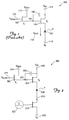
- FIG. 1 depicts an electrical schematic diagram of a typical AM OLED sub-pixel circuit 100 (labeled "Prior Art"), which is currently used in a conventional method for dimming an AM OLED display.
- conventional sub-pixel circuit 100 includes a first TFT 102, a second TFT 104, a storage capacitor 106, and an OLED pixel 108.
- transistor 102 is a scan transistor
- transistor 104 is a drive transistor.
- the gate terminal 110 of the scan transistor 102 is connected to the row (scan/row enable) address bus of the display involved, and the drain terminal 112 of scan transistor 102 is connected to the column (data) address bus of the display.
- the source of scan transistor 102 is connected to the node 107 at the storage capacitor 106 and the gate terminal of the drive transistor 104.
- scan transistor 102 charges the node 107 at the storage capacitor 106 and the gate terminal of the drive transistor 104 to the data voltage (signal), V DATA .
- V DATA data voltage
- scan transistor 102 is switched off, and the OLED pixel 108 is electrically isolated from the data bus.
- the power supply voltage, V DD which is connected to the drain terminal 114 of the drive transistor 104, provides the current for driving the OLED pixel 108.
- the present invention provides an improved AM OLED display and method of adjusting luminance with superior dimming capability (e.g., wide dynamic range > 2000 : 1) that resolves the problems encountered with existing AM OLED displays and other prior art displays.
- US-A-2003/0063078 discloses an organic electroluminescent (EL) display device that includes display pixels forming a display screen, scanning lines disposed along rows of the display pixels, signal lines disposed along columns of the display pixels, and a power supply section which supplies a power-supply voltage to the display pixels.
- Each of the display pixels includes a luminous element, a pixel switch and a driving element.
- Each luminous element is connected to the power supply section via a dimmer switch portion.
- three transistors, a capacitor and an organic EL element are used.
- US-A-2004/0041525 discloses an organic electro-luminescence device and method and apparatus for driving the same, using multiple transistors.
- a cell drive voltage source applies a drive voltage to the electro-luminescence cell, and a cathode terminal of the electro-luminescence cell is selectively connected to a common voltage source and a ground voltage source to have a reverse bias voltage applied.
- four transistors, a capacitor and an OLED are used.
- EP-A-1,197,943 discloses a driving circuit for an organic electroluminescent element, electronic equipment, and electro-optical device. Pixels are reverse-biased on the basis of a group of predetermined pixels at a time. In one embodiment, multiple transistors and capacitors are used.
- the present invention in its various aspects is as set out in the appended claims, and it provides an improved AM OLED pixel circuit of wide dynamic range dimming for AM OLED displays that maintains color balance throughout the dimming range, and also maintains the uniformity of the luminance and chromaticity of the display at low gray-levels as the display is dimmed to lower luminance values.
- the present invention enables AM OLED displays to meet the stringent color/dimming specifications required for existing and future avionics, cockpit, and hand-held military device display applications.
- the present invention provides an improved AM OLED pixel circuit of dynamic range dimming that uses Pulse Width Modulation (PWM) of the OLED pixel current to achieve the desired display luminance (brightness).
- PWM Pulse Width Modulation
- Two example embodiments of the invention are provided for externally (e.g., outside an AM OLED glass display) PW modulating the common cathode voltage (V k ) or common power supply voltage (V DD ) so as to modulate the OLED current in order to achieve the desired display luminance.
- Three additional example embodiments of the invention are provided that incorporate additional transistor switches in the pixel circuit in order to modulate the OLED current during the frame time. Unlike the conventional methods, the three additional (internal) example embodiments allow modulation of each row of pixels sequentially during the frame time, which eliminates any propensity for display flicker.
- PW modulating the OLED current in combination with data voltage (or current) modulation, the present invention achieves wide dynamic range dimming while maintaining the color balance and the luminance and chromaticity uniformity required over the surface of the display involved.
- Figure 2A depicts a pictorial representation of an example cockpit or avionics display environment 200A, which may be used as an environment to implement one or more embodiments of the present invention.
- Figure 2B depicts a pictorial representation of an example cockpit or avionics display 200B (e.g., from within the example environment 200A) including an example display 202B, in which one or more embodiments of the present invention may be implemented.
- Figures 2A and 2B depict an exemplary environment and avionics or cockpit display, the present invention is not intended to be so limited and can be implemented in any suitable display requiring, for example, wide dynamic range dimming (e.g., military or commercial hand-held device with flat panel display, etc.).
- FIG. 3 depicts an electrical schematic diagram of a comparative example AM OLED sub-pixel circuit 300.
- AM OLED sub-pixel circuit 300 can be used in a preferred method for dynamically dimming an AM OLED display using, for example, an external (to the display) PWM scheme.
- AM OLED sub-pixel circuit 300 includes a first TFT 302, a second TFT 304, a storage capacitor 306, an OLED pixel 308, and a transistor 310, represented here by a Field Effect Transistor (FET).
- FET Field Effect Transistor
- transistor 302 is a scan transistor
- transistor 304 is a drive transistor.
- an AM OLED display incorporating AM OLED pixel circuit 300 can include a plurality of (e.g., two or more) common cathode terminals, V K 320.
- One such common cathode terminal, V K 320 can be used to cover a top half of the display rows on the display involved, and another common cathode terminal, V K 320, can be used to cover a bottom half of the display rows on the display involved.
- a display can include 480 rows and 640 columns.
- Each of the common cathode terminals, V K 320, in such an AM OLED display can be switched to the cathode voltage through the transistor 310 controlled by a PWM signal generator 322.
- An example frequency for a PWM signal from generator 322 is 60 Hz.
- scan transistor 302 charges the node 307 at the storage capacitor 306 and the gate terminal of the drive transistor 304 to the data voltage (signal), V DATA .
- scan transistor 302 is switched off, and the OLED pixel 308 is electrically isolated from the data bus.
- the common cathode voltage, V K 320 is PW modulated by the signal applied from PWM signal generator 322, which functions to apply a reverse bias across the row(s) of OLED pixels (e.g., OLED pixel 308) associated with this common cathode terminal, V K 320, which in turn, switches "off" the OLED pixels (e.g., OLED pixel 308) associated with this common cathode terminal, V K 320, in order to control the brightness or luminance during the frame time of the display involved.
- an AM OLED pixel circuit and method are provided for achieving wide dynamic range dimming while maintaining the color balance and the luminance and chromaticity uniformity required over the surface of the display involved.
- FIG. 4 depicts an electrical schematic diagram of a comparative example AM OLED sub-pixel circuit 400.
- AM OLED sub-pixel circuit 400 can be used in a preferred method for dynamically dimming an AM OLED display using, for example, an external (to the display) PWM scheme.
- AM OLED sub-pixel circuit 400 includes a first TFT 402, a storage capacitor 404, a second TFT 408, an OLED pixel 410, and a transistor 406 represented here by a P-channel FET.
- an AM OLED display incorporating AM OLED sub-pixel circuit 400 can include a plurality of (e.g., two or more) common power supply voltage terminals, V DD 418.
- Each one of the common power supply voltages e.g., V DD 418 in Figure 4
- the control (e.g. gate) terminal of transistor 406 in such a display is connected to a PWM signal generator 420.
- scan transistor 412 charges the node 426 at the storage capacitor 404 and the gate terminal of the drive transistor 408 to the data voltage (signal), V DATA .
- scan transistor 412 is switched off, and the OLED pixel 410 is electrically isolated from the data bus.
- the PW modulated signal from PWM signal generator 420 is applied to the gate of the switch transistor 406, which PW modulates the common power supply voltage, V DD 418, to turn "off" the voltage across the plurality of OLED pixels (e.g., OLED pixel 410) associated with the common power supply voltage, V DD 418, and thus control the brightness of the overall display.
- the dimming of the display can be achieved with optimum uniformity.
- FIG. 5 depicts an electrical schematic diagram of a compaarative example AM OLED sub-pixel circuit 500.
- AM OLED sub-pixel circuit 500 can be used in a preferred method for dynamically dimming an AM OLED display using, for example, an internal (to the display) PWM scheme.
- AM OLED sub-pixel circuit 500 includes a first TFT 502, a storage capacitor 504, a second TFT 506, a third TFT 508, and an OLED pixel 510.
- a third TFT 508 (internal to the display involved) can be used at each sub-pixel in the display to PW modulate the current, I OLED 518, of the OLED pixel 510, in order to turn "off" the OLED pixel (e.g., OLED pixel 510) so that it does not emit light, and thus control the brightness of the overall display.
- the brightness of the display can be modulated (dimmed) by a factor of 1000:1 by the preset PWM method alone, and allowing the desired wide dynamic range dimming (e.g., > 2000:1) to be accomplished using gray-levels with higher luminance values.
- the desired wide dynamic range dimming e.g., > 2000:1
- scan transistor 502 charges the node 507 at the storage capacitor 504 and the gate terminal of the drive transistor 506 to the data voltage (signal), V DATA .
- scan transistor 502 is switched off, and the OLED pixel 510 is electrically isolated from the data bus.
- FIG. 6 depicts an electrical schematic diagram of a comparative example AM OLED sub-pixel circuit 600.
- AM OLED sub-pixel circuit 600 can be used in a preferred method for dynamically dimming an AM OLED display using, for example, an internal (to the display) PWM scheme.
- AM OLED sub-pixel circuit 600 includes a first TFT 602, a storage capacitor 604, a second TFT 606, a third TFT 608, and an OLED pixel 610.
Landscapes
- Engineering & Computer Science (AREA)
- Physics & Mathematics (AREA)
- Computer Hardware Design (AREA)
- General Physics & Mathematics (AREA)
- Theoretical Computer Science (AREA)
- Control Of Indicators Other Than Cathode Ray Tubes (AREA)
- Electroluminescent Light Sources (AREA)
Description
- The present invention relates generally to the field of flat panel displays, and more specifically, but not exclusively, to an improved Active Matrix Organic Light Emitting Diode (AM OLED) display and method of wide dynamic range dimming in such a display for commercial and military applications, such as, for example, cockpit displays, avionics displays, or hand-held military communication device displays.
- AM OLED displays are an emerging flat panel display technology, which has already produced such new products as passive matrix-addressed displays that can be used for cell-phones and automobile audio systems. AM OLED displays are most likely to replace backlit AM Liquid Crystal Displays (LCDs) because AM OLED displays are more power efficient, rugged, weigh less, cost less, and have much better image quality than existing AM LCDs. As such, the market for AM OLED-based displays is estimated to reach about $1.7B per year by 2006.
- Cockpit display applications are relatively demanding for existing display technologies, because of the stringent requirements imposed with respect to image quality and the need for superior operational performance within a broad range of environments, such as high temperature, humidity, and ambient lighting environments. For the better part of the past ten years, AM LCDs have replaced Cathode Ray Tube (CRT) displays in cockpit applications, because of the advantages of AM LCDs over CRT displays in terms of lower weight, flatter form factor, less power consumption, the use of large active areas with relatively small bezels, higher reliability, higher luminance, greater luminance uniformity, wider dimming range, and better sunlight readability. As such, AM LCDs have been the displays of choice for cockpit and avionics display applications for a number of years.
- A significant problem that exists with AM LCDs for display applications (e.g., cockpit, avionics and hand-held device displays) is that the backlighting of the AM LCDs adds a significant amount of weight and volume to these types of displays. However, an advantage of this backlighting feature of AM LCDs is that it provides a highly controllable function for (independently) dimming the display in order to achieve optimum performance over a range of ambient lighting conditions. Some critical display applications (e.g., avionics and certain military device displays) require wide dynamic ranges of dimming (e.g., > 2000:1) for the display to be viewed comfortably in both daytime (bright) and night-time (dark) viewing conditions. Currently, this dimming function can be accomplished with AM LCDs by dimming the display backlight (through a large dynamic range), while maintaining the AM LCD's optimized driving conditions.
- The weight and volume problems that exist with AM LCDs for avionics or hand-held device applications, for example, can be alleviated with AM OLED displays. Compared to AM LCDs, AM OLED displays offer such significant advantages as wider viewing angles, lower power consumption, lighter weight, superior response time, superior image quality, and lower cost. However, a drawback of the existing AM OLED displays is that they are not easily dimmable (i.e., their brightness adjusted) to the desired luminance levels, except by changing the driving conditions of the AM OLED displays, or by varying the anode (VDD) and/or cathode (VK) voltages.
- Generally, the existing AM OLED displays' grayscale driving conditions are optimized for "normal" daytime (bright ambient) viewing conditions. However, changing either the grayscale driving conditions or the VDD/VK voltages of AM OLED displays to achieve lower display luminance levels for night (dark ambient) conditions using a conventional AM OLED display results in luminance and color non-uniformities across the surfaces of these displays.
- As such, an important requirement imposed on AM OLED displays in such critical applications as cockpit displays, avionics displays, or military hand-held device displays is that such displays have to be capable of adjusting their luminance (brightness) over a wide dynamic range (e.g., >2000:1) without affecting the color balance and/or the uniformity of the luminance and chromaticity across the surface of the display as the display is being dimmed. The drive methods used for existing AM OLED displays achieve the desired luminance by adjusting the grayscale data voltage (or current) or VDD/VK voltage(s). However, these existing methods of adjusting the luminance of AM OLED displays create numerous problems for wide dynamic range display dimming applications, such as: (1) it is a relatively difficult problem to achieve the desired wide dynamic range dimming requirements with the existing driving methods using 8-bit data (column) drivers currently available for AM OLED displays; (2) when the grayscale data voltages (or currents) or the VDD/VK voltages, which are optimized for "normal" daylight operation, are changed (e.g., reduced) for night-time (low luminance) operation, typically the display color balance is changed due to the different transfer characteristics (luminance versus voltage) for the Red, Green and Blue (R, G, B) AM OLED display materials used; and (3) operation of the existing AM OLED displays at the low luminance levels associated with night-time viewing conditions results in significant non-uniformities in the luminance and chromaticity across the surface of the displays due to increased variations in the Thin-Film Transistor (TFT) and OLED performance in the low luminance (gray-level) regime.
- As such, to illustrate these problems with existing AM OLED displays,
Figure 1 depicts an electrical schematic diagram of a typical AM OLED sub-pixel circuit 100 (labeled "Prior Art"), which is currently used in a conventional method for dimming an AM OLED display. Referring toFigure 1 ,conventional sub-pixel circuit 100 includes afirst TFT 102, asecond TFT 104, astorage capacitor 106, and anOLED pixel 108. As shown,transistor 102 is a scan transistor, andtransistor 104 is a drive transistor. Thegate terminal 110 of thescan transistor 102 is connected to the row (scan/row enable) address bus of the display involved, and thedrain terminal 112 ofscan transistor 102 is connected to the column (data) address bus of the display. The source ofscan transistor 102 is connected to thenode 107 at thestorage capacitor 106 and the gate terminal of thedrive transistor 104. During the row addressing time period of the display operation,scan transistor 102 charges thenode 107 at thestorage capacitor 106 and the gate terminal of thedrive transistor 104 to the data voltage (signal), VDATA. After the row addressing time period,scan transistor 102 is switched off, and theOLED pixel 108 is electrically isolated from the data bus. During the remainder of the frame time, the power supply voltage, VDD, which is connected to thedrain terminal 114 of thedrive transistor 104, provides the current for driving theOLED pixel 108. - The grayscale from this conventional method in the AM
OLED display circuit 100 depicted inFigure 1 is achieved by varying the data voltages (signals) on the data bus. In addition, the brightness (maximum luminance) of the display is adjusted (for display dimming) directly by changing the data voltages (signals) or VDD/VK voltages. However, as discussed earlier, it can be seen fromFigure 1 that a significant problem with these conventional methods of adjusting the luminance of an AM OLED display is that because the dimming is performed by changing the data voltage (or current), or by changing the power supply (VDD and/or Vk) voltages to adjust the grayscale, wide dynamic range dimming (e.g., > 2000: 1) cannot be achieved with suitable uniformity. Nevertheless, as described in detail below, the present invention provides an improved AM OLED display and method of adjusting luminance with superior dimming capability (e.g., wide dynamic range > 2000 : 1) that resolves the problems encountered with existing AM OLED displays and other prior art displays. -
US-A-2003/0063078 discloses an organic electroluminescent (EL) display device that includes display pixels forming a display screen, scanning lines disposed along rows of the display pixels, signal lines disposed along columns of the display pixels, and a power supply section which supplies a power-supply voltage to the display pixels. Each of the display pixels includes a luminous element, a pixel switch and a driving element. Each luminous element is connected to the power supply section via a dimmer switch portion. In one embodiment, three transistors, a capacitor and an organic EL element are used. -
US-A-2004/0041525 discloses an organic electro-luminescence device and method and apparatus for driving the same, using multiple transistors. A cell drive voltage source applies a drive voltage to the electro-luminescence cell, and a cathode terminal of the electro-luminescence cell is selectively connected to a common voltage source and a ground voltage source to have a reverse bias voltage applied. In one embodiment, four transistors, a capacitor and an OLED are used. -
EP-A-1,197,943 discloses a driving circuit for an organic electroluminescent element, electronic equipment, and electro-optical device. Pixels are reverse-biased on the basis of a group of predetermined pixels at a time. In one embodiment, multiple transistors and capacitors are used. - The invention is set forth in claim 1.
- The present invention in its various aspects is as set out in the appended claims, and it provides an improved AM OLED pixel circuit of wide dynamic range dimming for AM OLED displays that maintains color balance throughout the dimming range, and also maintains the uniformity of the luminance and chromaticity of the display at low gray-levels as the display is dimmed to lower luminance values. As such, the present invention enables AM OLED displays to meet the stringent color/dimming specifications required for existing and future avionics, cockpit, and hand-held military device display applications. Essentially, the present invention provides an improved AM OLED pixel circuit of dynamic range dimming that uses Pulse Width Modulation (PWM) of the OLED pixel current to achieve the desired display luminance (brightness).
- Two example embodiments of the invention are provided for externally (e.g., outside an AM OLED glass display) PW modulating the common cathode voltage (Vk) or common power supply voltage (VDD) so as to modulate the OLED current in order to achieve the desired display luminance. Three additional example embodiments of the invention are provided that incorporate additional transistor switches in the pixel circuit in order to modulate the OLED current during the frame time. Unlike the conventional methods, the three additional (internal) example embodiments allow modulation of each row of pixels sequentially during the frame time, which eliminates any propensity for display flicker. Thus, by PW modulating the OLED current, in combination with data voltage (or current) modulation, the present invention achieves wide dynamic range dimming while maintaining the color balance and the luminance and chromaticity uniformity required over the surface of the display involved.
- The novel features believed characteristic of the invention are set forth in the appended claims. The invention itself, however, as well as a preferred mode of use, further objectives and advantages thereof, will best be understood by reference to the following detailed description of an illustrative embodiment when read in conjunction with the accompanying drawings, wherein:
-
Figure 1 depicts an electrical schematic diagram of a prior art AM OLED sub-pixel circuit, which is currently used in a conventional method for dimming an AM OLED display; -
Figure 2A depicts a pictorial representation of an example cockpit or avionics display environment, which may be used as an environment to implement one or more embodiments of the present invention; -
Figure 2B depicts a pictorial representation of an example cockpit or avionics display, in which one or more embodiments of the present invention may be implemented; -
Figure 3 depicts an electrical schematic diagram of a comparative example AM OLED sub-pixel circuit; -
Figure 4 depicts an electrical schematic diagram of a comparative example AM OLED sub-pixel circuit; -
Figure 5 depicts an electrical schematic diagram of a comparative example AM OLED sub-pixel circuit; -
Figure 6 depicts an electrical schematic diagram of a comparative example AM OLED sub-pixel circuit; -
Figure 7 depicts an electrical schematic diagram of an example AM OLED sub-pixel circuit, which can be used to implement an embodiment of the present invention. - With reference now to the figures,
Figure 2A depicts a pictorial representation of an example cockpit oravionics display environment 200A, which may be used as an environment to implement one or more embodiments of the present invention.Figure 2B depicts a pictorial representation of an example cockpit oravionics display 200B (e.g., from within theexample environment 200A) including anexample display 202B, in which one or more embodiments of the present invention may be implemented. As such, althoughFigures 2A and 2B depict an exemplary environment and avionics or cockpit display, the present invention is not intended to be so limited and can be implemented in any suitable display requiring, for example, wide dynamic range dimming (e.g., military or commercial hand-held device with flat panel display, etc.). -
Figure 3 depicts an electrical schematic diagram of a comparative example AMOLED sub-pixel circuit 300. As such, AMOLED sub-pixel circuit 300 can be used in a preferred method for dynamically dimming an AM OLED display using, for example, an external (to the display) PWM scheme. Referring now toFigure 3 , AMOLED sub-pixel circuit 300 includes a first TFT 302, asecond TFT 304, astorage capacitor 306, anOLED pixel 308, and atransistor 310, represented here by a Field Effect Transistor (FET). As shown, transistor 302 is a scan transistor, andtransistor 304 is a drive transistor. Thegate terminal 312 of the scan transistor 302 is connected to the row (scan/row enable) address bus of the display involved, and thedrain terminal 314 of scan transistor 302 is connected to the column (data) address bus of the display. The source of scan transistor 302 is connected to thenode 307 at thestorage capacitor 306 and the gate terminal of thedrive transistor 304. The source ofdrive transistor 304 is connected to a terminal ofOLED pixel 308. Thesecond terminal 318 ofOLED pixel 308 is connected to one (e.g. drain) terminal oftransistor 310. The other (e.g. source) terminal oftransistor 310 is connected to a common cathode terminal,V K 320. - For this example, an AM OLED display incorporating AM
OLED pixel circuit 300 can include a plurality of (e.g., two or more) common cathode terminals,V K 320. One such common cathode terminal,V K 320, can be used to cover a top half of the display rows on the display involved, and another common cathode terminal,V K 320, can be used to cover a bottom half of the display rows on the display involved. For example, a display can include 480 rows and 640 columns. Each of the common cathode terminals,V K 320, in such an AM OLED display can be switched to the cathode voltage through thetransistor 310 controlled by a PWM signal generator 322. An example frequency for a PWM signal from generator 322 is 60 Hz. - During the row addressing time period of the display operation, scan transistor 302 charges the
node 307 at thestorage capacitor 306 and the gate terminal of thedrive transistor 304 to the data voltage (signal), VDATA. After the row addressing time period, scan transistor 302 is switched off, and theOLED pixel 308 is electrically isolated from the data bus. - For this example, the common cathode voltage,
V K 320, is PW modulated by the signal applied from PWM signal generator 322, which functions to apply a reverse bias across the row(s) of OLED pixels (e.g., OLED pixel 308) associated with this common cathode terminal,V K 320, which in turn, switches "off" the OLED pixels (e.g., OLED pixel 308) associated with this common cathode terminal,V K 320, in order to control the brightness or luminance during the frame time of the display involved. Thus, in accordance with this example, an AM OLED pixel circuit and method are provided for achieving wide dynamic range dimming while maintaining the color balance and the luminance and chromaticity uniformity required over the surface of the display involved. In this case, anexternal transistor 310 can be used to modulate the cathode power supply,V K 320, of theOLED pixel 308 in order to dynamically dim the display. Thus, by PW modulating the common cathode voltage,V K 320, the luminance or brightness of the display is averaged over a suitable period of time. Therefore, using the PWM method allows significantly more uniform dimming of OLED displays than currently provided for the existing OLED displays. -
Figure 4 depicts an electrical schematic diagram of a comparative example AMOLED sub-pixel circuit 400. As such, AMOLED sub-pixel circuit 400 can be used in a preferred method for dynamically dimming an AM OLED display using, for example, an external (to the display) PWM scheme. Referring now toFigure 4 , AMOLED sub-pixel circuit 400 includes afirst TFT 402, astorage capacitor 404, a second TFT 408, anOLED pixel 410, and atransistor 406 represented here by a P-channel FET. In this case, an external (to the display involved)transistor 406 can be used to PW modulate the positive power supply,V DD 418, of theOLED pixel 410, in order to turn "off" the voltage across the OLED pixels (e.g., OLED pixel 410) associated with the common power supply voltage,V DD 418, and thus to control the brightness of the display. Also, in this case, the reference voltage,V SC 416, forstorage capacitor 404, can be removed from the VDD line to prevent coupling the PW modulated VDD to the gate voltage, VGS2, at thenode 426 between the gate terminal of transistor 408 andstorage capacitor 404. - As shown, for this example,
transistor 402 is a scan transistor, and transistor 408 is a drive transistor. Thegate terminal 412 of thescan transistor 402 is connected to the row (scan/row enable) address bus of the display involved, and thedrain terminal 414 ofscan transistor 402 is connected to the column (data) address bus of the display. The source ofscan transistor 402 is connected to thenode 426 at thestorage capacitor 404 and the gate terminal of the drive transistor 408. The source of drive transistor 408 is connected to a terminal ofOLED pixel 410. The drain of drive transistor 408 is connected to one (e.g. the drain)terminal 422 of thetransistor 406, and the other (e.g. the source) terminal oftransistor 406 is connected to the common power supply voltage,V DD 418. The second terminal ofOLED pixel 410 is connected to a common cathode terminal,V K 424. - For this example, an AM OLED display incorporating AM
OLED sub-pixel circuit 400 can include a plurality of (e.g., two or more) common power supply voltage terminals,V DD 418. Each one of the common power supply voltages (e.g.,V DD 418 inFigure 4 ) provides the positive power supply voltage for the particular OLED sub-pixel involved (e.g., OLED 410) within the overall display. The control (e.g. gate) terminal oftransistor 406 in such a display is connected to aPWM signal generator 420. - During the row addressing time period of the display operation,
scan transistor 412 charges thenode 426 at thestorage capacitor 404 and the gate terminal of the drive transistor 408 to the data voltage (signal), VDATA. After the row addressing time period,scan transistor 412 is switched off, and theOLED pixel 410 is electrically isolated from the data bus. Then, in order to adjust the luminance (e.g., brightness) of the display (e.g., OLED pixel 410), the PW modulated signal fromPWM signal generator 420 is applied to the gate of theswitch transistor 406, which PW modulates the common power supply voltage,V DD 418, to turn "off" the voltage across the plurality of OLED pixels (e.g., OLED pixel 410) associated with the common power supply voltage,V DD 418, and thus control the brightness of the overall display. Again, using the PWM method, the dimming of the display can be achieved with optimum uniformity. -
Figure 5 depicts an electrical schematic diagram of a compaarative example AMOLED sub-pixel circuit 500. As such, AMOLED sub-pixel circuit 500 can be used in a preferred method for dynamically dimming an AM OLED display using, for example, an internal (to the display) PWM scheme. Referring now toFigure 5 , AMOLED sub-pixel circuit 500 includes afirst TFT 502, astorage capacitor 504, asecond TFT 506, athird TFT 508, and anOLED pixel 510. In this case, a third TFT 508 (internal to the display involved) can be used at each sub-pixel in the display to PW modulate the current, IOLED 518, of theOLED pixel 510, in order to turn "off" the OLED pixel (e.g., OLED pixel 510) so that it does not emit light, and thus control the brightness of the overall display. - As shown, for this example,
transistor 502 is a scan transistor, andtransistor 506 is a drive transistor. Thegate terminal 512 of thescan transistor 502 is connected to the row (scan/row enable) address bus of the display involved, and thedrain terminal 514 ofscan transistor 502 is connected to the column (data) address bus of the display. The source ofscan transistor 502 is connected to thenode 507 at thestorage capacitor 504 and the gate terminal of thedrive transistor 506. The source ofdrive transistor 506 is connected to the drain of thethird TFT 508, and the source ofthird TFT 508 is connected to a terminal ofOLED pixel 510. The drain ofdrive transistor 506 is connected to the common power supply voltage,V DD 516. The second terminal ofOLED pixel 510 is connected to a common cathode terminal,V K 522. - For this example, an AM OLED display incorporating AM
OLED sub-pixel circuit 500 can include a plurality of (e.g., two or more) PWM voltage signal generators,V PWM 520. Thus, by pixel switching or PWM of thethird TFT 508, thethird TFT 508 controls the OLED current IOLED 518 and switches "off" the OLED pixel involved (e.g.,OLED pixel 510 inFigure 5 ) so that the OLED pixel involved does not emit light. - Specifically, the gate terminal of the switching
TFT 508, in each of the pixels in a given row in the display, is connected to a row bus that is addressable from outside the display, as is the row-enable bus. The PW modulated signal, VpWM, from the PWMvoltage signal generator 520, is applied to each row in order to switch "off" the current flow to theOLED pixel 510 and turn the pixel "off". The "on" time of each of the rows is modulated to control the brightness of the display. A significant amount of modulation (e.g., dimming) can be achieved using such an internal modulation scheme. - For example, in a 1000 line (rows) display, the brightness of the display can be modulated (dimmed) by a factor of 1000:1 by the preset PWM method alone, and allowing the desired wide dynamic range dimming (e.g., > 2000:1) to be accomplished using gray-levels with higher luminance values. Thus, it significantly improves the uniformity of the luminance and chromaticity across the surface of the display as it is being dimmed, as compared to the conventional dimming methods used for AM OLED displays.
- As such, the PWM
voltage signal generator 520 can be commonly connected to all of the pixels in the display, or each row of pixels can be provided with an independent PWM signal generator (e.g., such as PWM voltage signal generator 520). Incidentally, an advantage of providing each row of pixels with a separate PWM voltage (e.g., VPWM 520), is that the display flicker can be significantly minimized in comparison to other approaches. - During the row addressing time period of the display operation,
scan transistor 502 charges thenode 507 at thestorage capacitor 504 and the gate terminal of thedrive transistor 506 to the data voltage (signal), VDATA. After the row addressing time period,scan transistor 502 is switched off, and theOLED pixel 510 is electrically isolated from the data bus. Then, in order to adjust the luminance (e.g., brightness) of the display (e.g., OLED pixel 510), the PW modulated signal, VPWM, from PWMvoltage signal generator 520 is applied to the gate of thethird TFT 508, which PW modulates the OLED current, IOLED 518, to turn "off" the subject OLED pixels (e.g., OLED pixel 510), and thus control the brightness of the overall display. Again, using the PWM method of the present invention, the dimming of the display can be achieved with optimum uniformity. -
Figure 6 depicts an electrical schematic diagram of a comparative example AMOLED sub-pixel circuit 600. As such, AMOLED sub-pixel circuit 600 can be used in a preferred method for dynamically dimming an AM OLED display using, for example, an internal (to the display) PWM scheme. Referring now toFigure 6 , AMOLED sub-pixel circuit 600 includes afirst TFT 602, astorage capacitor 604, asecond TFT 606, athird TFT 608, and anOLED pixel 610. In this case, a third TFT 608 (internal to the display involved) can be used at each sub-pixel in the display to PW modulate the current through the OLED pixel involved in order to turn "off" that OLED pixel (e.g., OLED pixel 610) so that it does not emit light, and thus control the brightness of the overall display. - As shown, for this example,
transistor 602 is a scan transistor, andtransistor 606 is a drive transistor. Thegate terminal 612 of thescan transistor 602 is connected to the row (scan/row enable) address bus of the display involved, and thedrain terminal 614 ofscan transistor 602 is connected to the column (data) address bus of the display. The source ofscan transistor 602 is connected to thenode 620 at thestorage capacitor 604, the drain ofthird TFT 608, and the gate terminal of thedrive transistor 606. The source of thedrive transistor 606 is connected to the source of thethird TFT 608 and one terminal ofOLED pixel 610. The drain terminal ofdrive transistor 606 is connected to the common power supply voltage,V DD 618. The second terminal ofOLED pixel 610 is connected to a common cathode terminal,V K 622. - For this example, an AM OLED display incorporating AM
OLED sub-pixel circuit 600 can include a plurality of (e.g., two or more) PWM voltage signal generators,Vp WM 624. Thus, by PWM of the gate voltage,V GS2 620, at the gate of thedrive transistor 606, thethird TFT 608 can control the current through the OLED pixel involved (e.g., OLED pixel 610) by turning "off" thedrive transistor 606 and, therefore, turning "off" the OLED pixel involved (e.g.,OLED pixel 610 inFigure 6 ) so that the OLED pixel involved does not emit light. As such, the PWMvoltage signal generator 624 can be common to all of the pixels in the display, or each row of pixels can be provided with an independent PWM signal generator (e.g., such as PWM voltage signal generator 624). Once again, an advantage of providing each row of pixels with a separate PWM voltage (e.g., VpWM 624), is that the present method can significantly reduce the display's propensity for flicker in comparison with other existing approaches. - During the row addressing time period of the display operation,
scan transistor 602 charges thenode 620 at thestorage capacitor 604 and the gate terminal of thedrive transistor 606 to the data voltage (signal), VDATA. After the row addressing time period,scan transistor 602 is switched off, and theOLED pixel 610 is electrically isolated from the data bus. Then, in order to adjust the luminance (e.g., brightness) of the display (e.g., OLED pixel 610), the PW modulated signal, VPWM, from PWMvoltage signal generator 624 is applied to the gate of thethird TFT 608, which PW modulates the gate voltage,V GS2 620, and turns "off" thedrive transistor 606. In response, PW modulation of thedrive transistor 606 controls the current through the OLED pixel involved, and turns "off" the subject OLED pixel (e.g., OLED pixel 610) to control the brightness of the overall display. Again, using the PWM method, the dimming of the display can be achieved with optimum uniformity. -
Figure 7 depicts an electrical schematic diagram of an example AMOLED sub-pixel circuit 700, which can be used to implement an embodiment of the present invention. As such, AMOLED sub-pixel circuit 700 can be used in a preferred method for dynamically dimming an AM OLED display using, for example, an internal (to the display) PWM scheme. Referring now toFigure 7 , AMOLED sub-pixel circuit 700 includes afirst TFT 702, astorage capacitor 706, asecond TFT 710, athird TFT 704, afourth TFT 712, and anOLED pixel 714. In this case, two additional transistors (e.g.,third TFT 704 and fourth TFT 712), which are both internal to the display involved, can be used at each sub-pixel in the display to enable PWM of the current through the OLED pixel involved (e.g., IOLED 718), in order to turn "off" that OLED pixel (e.g., OLED pixel 714) so that it does not emit light, by changing the gate voltage,V GS2 716, from a pre-selected value to "off". At a selected time after thestorage capacitor 706 is charged to the pre-selected value, the PWM voltage,V PWM 730, goes high, which shuts "off"third TFT 704 and (e.g., disconnectingV C 706 from VGS2 716) and turns "on"fourth TFT 712, which in turn, shuts "off"drive transistor 710. This PWM method of the present invention thus controls the current through theOLED pixel 714 involved (e.g., IOLED 718), which controls the brightness of the overall display. - As mentioned earlier, a significant advantage of providing each row of pixels with a separate PWM voltage (e.g., VpWM 730), is that the present method can significantly reduce the display's propensity for flicker in comparison with other existing approaches. Also, using the PWM method of the present invention, the dimming of the AM OLED display can be achieved with optimum uniformity.
- It is important to note that while the present invention has been described in the context of a fully functioning AM OLED display, those of ordinary skill in the art will appreciate that the processes of the present invention are capable of being distributed in the form of a computer readable medium of instructions and a variety of forms and that the present invention applies equally regardless of the particular type of signal bearing media actually used to carry out the distribution. Examples of computer readable media include recordable-type media, such as a floppy disk, a hard disk drive, a RAM, CD-ROMs, DVD-ROMs, and transmission-type media, such as digital and analog communications links, wired or wireless communications links using transmission forms, such as, for example, radio frequency and light wave transmissions. The computer readable media may take the form of coded formats that are decoded for actual use in a particular AM OLED display.
- The description of the present invention has been presented for purposes of illustration and description, and is not intended to be exhaustive or limited to the invention in the form disclosed. Many modifications and variations will be apparent to those of ordinary skill in the art. These embodiments were chosen and described in order to best explain the principles of the invention, the practical application, and to enable others of ordinary skill in the art to understand the invention for various embodiments with various modifications as are suited to the particular use contemplated.
Claims (1)
- An Organic Light Emitting Diode display, comprising: at least one row address bus (720), at least one column address bus, a common power supply voltage (724), a common cathode terminal (728), a Pulse Width Modulation voltage signal generator (730), and at least a sub-pixel circuit (700), the sub-pixel circuit (730) including a first thin film transistor (702), a second thin film transistor (710), a third thin film transistor (704), a fourth thin film transistor (712), a storage capacitor (706), and an Organic Light Emitting Diode pixel (714), wherein
said first thin film transistor (702) is coupled by its gate to the row address bus (720), coupled by one of its source and drain to the column address bus (722), and by the other of the source and drain to one terminal (707) of said storage capacitor (706) and to one of the source and drain of said third thin film transistor (704);
said storage capacitor (706) is connected by its other terminal to the common power supply voltage (724) and to one of the source and drain of the second thin film transistor (710);
said Organic Light Emitting Diode (714) is coupled by its cathode to the common cathode terminal (728), and by its anode (719) to the other of the source and drain of the second thin film transistor (710), and to one of the source and drain of the fourth thin film transistor (712);
said second thin film transistor (710) is coupled by its gate to the other of the source and drain of the third thin film transistor (704), and to the other of the source and drain of the fourth thin film transistor (712); and
said third thin film transistor (704) and said fourth thin film transistor (712) are both coupled by their gates to the means for generating a Pulse Width Modulation signal (730)
and wherein said third thin film transistor and said fourth thin film transistor are arranged to shut off the third thin film transistor and turn on the fourth thin film transistor in response to the pulse width modulation signal being high.
Applications Claiming Priority (2)
| Application Number | Priority Date | Filing Date | Title |
|---|---|---|---|
| US11/043,657 US20060164345A1 (en) | 2005-01-26 | 2005-01-26 | Active matrix organic light emitting diode display |
| PCT/US2006/000626 WO2006081061A1 (en) | 2005-01-26 | 2006-01-10 | Active matrix organic light emitting diode display |
Publications (2)
| Publication Number | Publication Date |
|---|---|
| EP1846910A1 EP1846910A1 (en) | 2007-10-24 |
| EP1846910B1 true EP1846910B1 (en) | 2016-09-28 |
Family
ID=36499979
Family Applications (1)
| Application Number | Title | Priority Date | Filing Date |
|---|---|---|---|
| EP06717786.5A Ceased EP1846910B1 (en) | 2005-01-26 | 2006-01-10 | Active matrix organic light emitting diode display |
Country Status (7)
| Country | Link |
|---|---|
| US (3) | US20060164345A1 (en) |
| EP (1) | EP1846910B1 (en) |
| JP (1) | JP5203716B2 (en) |
| KR (1) | KR101258857B1 (en) |
| CN (2) | CN101147185A (en) |
| TW (1) | TWI413068B (en) |
| WO (1) | WO2006081061A1 (en) |
Cited By (1)
| Publication number | Priority date | Publication date | Assignee | Title |
|---|---|---|---|---|
| WO2021064061A1 (en) | 2019-10-01 | 2021-04-08 | Barco N.V. | Driver for led or oled display and drive circuit |
Families Citing this family (87)
| Publication number | Priority date | Publication date | Assignee | Title |
|---|---|---|---|---|
| JP2008287141A (en) | 2007-05-21 | 2008-11-27 | Sony Corp | Display device, driving method thereof, and electronic apparatus |
| US7956831B2 (en) * | 2007-05-30 | 2011-06-07 | Honeywell Interntional Inc. | Apparatus, systems, and methods for dimming an active matrix light-emitting diode (LED) display |
| US8264482B2 (en) * | 2007-12-19 | 2012-09-11 | Global Oled Technology Llc | Interleaving drive circuit and electro-luminescent display system utilizing a multiplexer |
| US8044984B2 (en) * | 2008-03-27 | 2011-10-25 | Himax Technologies Limited | Methods for driving an OLED panel |
| US8771078B2 (en) | 2009-06-08 | 2014-07-08 | Cfph, Llc | Amusement device including means for processing electronic data in play of a game of chance |
| US8545328B2 (en) * | 2009-06-08 | 2013-10-01 | Cfph, Llc | Portable electronic charge device for card devices |
| US8613671B2 (en) | 2009-06-08 | 2013-12-24 | Cfph, Llc | Data transfer and control among multiple computer devices in a gaming environment |
| US8784189B2 (en) | 2009-06-08 | 2014-07-22 | Cfph, Llc | Interprocess communication regarding movement of game devices |
| US8545327B2 (en) * | 2009-06-08 | 2013-10-01 | Cfph, Llc | Amusement device including means for processing electronic data in play of a game in which an outcome is dependant upon card values |
| US20110069089A1 (en) * | 2009-09-23 | 2011-03-24 | Microsoft Corporation | Power management for organic light-emitting diode (oled) displays |
| CN101916542B (en) * | 2010-01-05 | 2013-06-12 | 利亚德光电股份有限公司 | Image display device of LED panel television |
| KR20120028426A (en) | 2010-09-14 | 2012-03-23 | 삼성모바일디스플레이주식회사 | Organic light emitting display device and driving method thereof |
| FR2966276B1 (en) | 2010-10-15 | 2013-03-08 | Commissariat Energie Atomique | ACTIVE MATRIX LIGHT-EMITTING DIODE DISPLAY SCREEN WITH MEANS OF MITIGATION |
| CN101996580A (en) * | 2010-11-10 | 2011-03-30 | 南开大学 | Silicon-based active organic light emitting diode (OLED) display pixel circuit |
| CN102074193A (en) * | 2010-12-29 | 2011-05-25 | 广东中显科技有限公司 | Silicon-based OLED display screen and driving circuit thereof |
| JP5699282B2 (en) * | 2011-03-24 | 2015-04-08 | パナソニックIpマネジメント株式会社 | Organic electroluminescence device and lighting apparatus |
| CN102522064B (en) * | 2011-12-14 | 2014-01-29 | 中国航空无线电电子研究所 | Cabin controller with color OLED (Organic Light Emitting Diode) display screen |
| US9747834B2 (en) * | 2012-05-11 | 2017-08-29 | Ignis Innovation Inc. | Pixel circuits including feedback capacitors and reset capacitors, and display systems therefore |
| KR20140058283A (en) | 2012-11-06 | 2014-05-14 | 삼성디스플레이 주식회사 | Display device and method of driving thereof |
| JP2014002417A (en) * | 2013-09-24 | 2014-01-09 | Semiconductor Energy Lab Co Ltd | Semiconductor device, display device, display module and electronic apparatus |
| US9640114B2 (en) | 2014-06-19 | 2017-05-02 | Stmicroelectronics International N.V. | Device comprising a matrix of active OLED pixels with brightness adjustment, and corresponding method |
| CN104299573B (en) | 2014-11-13 | 2016-06-29 | 京东方科技集团股份有限公司 | A kind of image element circuit, display floater and driving method thereof |
| KR102382591B1 (en) | 2014-11-21 | 2022-04-04 | 삼성디스플레이 주식회사 | Organic light emitting diode display |
| US20160163278A1 (en) * | 2014-12-08 | 2016-06-09 | Pixtronix, Inc. | Signal adjustment circuit |
| CN104599637A (en) * | 2015-02-11 | 2015-05-06 | 京东方科技集团股份有限公司 | Pixel circuit drive method and drive device |
| US9881554B2 (en) | 2015-02-11 | 2018-01-30 | Boe Technology Group Co., Ltd. | Driving method of pixel circuit and driving device thereof |
| KR102438780B1 (en) | 2015-08-28 | 2022-09-02 | 삼성디스플레이 주식회사 | Display device and its driving method |
| KR101731178B1 (en) * | 2015-10-02 | 2017-04-28 | 엘지디스플레이 주식회사 | Organic Light Emitting Display and Method of Driving the same |
| WO2021035414A1 (en) * | 2019-08-23 | 2021-03-04 | 京东方科技集团股份有限公司 | Pixel circuit and driving method therefor, and display substrate and driving method therefor, and display device |
| CN106803418A (en) * | 2015-11-25 | 2017-06-06 | 上海和辉光电有限公司 | Method for displaying image, the drive circuit shown for image and display device |
| US9871965B2 (en) * | 2016-02-03 | 2018-01-16 | Texas Instruments Incorporated | Image processing for wide dynamic range (WDR) sensor data |
| KR102587794B1 (en) * | 2016-03-02 | 2023-10-12 | 삼성전자주식회사 | Image Display Apparatus and Driving Method Thereof |
| US10102795B2 (en) * | 2016-06-06 | 2018-10-16 | Mikro Mesa Technology Co., Ltd. | Operating method of display device and display device |
| JP2018063351A (en) * | 2016-10-13 | 2018-04-19 | 株式会社ジャパンディスプレイ | Organic el display device and method for driving organic el display device |
| CN106652903B (en) * | 2017-03-03 | 2018-10-23 | 京东方科技集团股份有限公司 | A kind of OLED pixel circuit and its driving method, display device |
| CN107068059B (en) * | 2017-05-27 | 2019-10-08 | 北京大学深圳研究生院 | Pixel arrangement, the method for driving pixel arrangement and display equipment |
| US11335301B2 (en) | 2017-06-30 | 2022-05-17 | Kunshan Go-Visionox Opto-Electronics Co., Ltd. | Devices and methods for dimming a display screen |
| CN109215549B (en) * | 2017-06-30 | 2021-01-22 | 昆山国显光电有限公司 | Display screen dimming method and device, storage medium and electronic equipment |
| CN107393480B (en) * | 2017-07-31 | 2020-07-28 | 京东方科技集团股份有限公司 | Display device and brightness adjusting method thereof |
| WO2019095298A1 (en) * | 2017-11-17 | 2019-05-23 | 深圳市柔宇科技有限公司 | Pixel circuit, flexible display screen and electronic device |
| CN113077760B (en) * | 2017-12-11 | 2022-11-01 | 成都晶砂科技有限公司 | Driving method of pixel driving circuit |
| CN109920372B (en) * | 2017-12-12 | 2021-01-29 | 京东方科技集团股份有限公司 | Display driving module, display device and voltage adjusting method |
| CN107993609A (en) * | 2018-03-16 | 2018-05-04 | 成都晶砂科技有限公司 | Method, system and the drive circuit that analog- and digital- combination drive display unit is shown |
| EP3776523B1 (en) | 2018-03-29 | 2026-03-11 | Barco n.v. | Driver for led display |
| US10694597B2 (en) * | 2018-04-19 | 2020-06-23 | Innolux Corporation | LED pixel circuits with PWM dimming |
| CN108320712A (en) * | 2018-04-27 | 2018-07-24 | 江苏集萃有机光电技术研究所有限公司 | Pixel circuit and display device |
| CN108630151B (en) * | 2018-05-17 | 2022-08-26 | 京东方科技集团股份有限公司 | Pixel circuit, driving method thereof, array substrate and display device |
| CN115424562A (en) * | 2018-06-28 | 2022-12-02 | 萨皮恩半导体公司 | Pixel and display device including the same |
| CN110728946A (en) * | 2018-06-29 | 2020-01-24 | 京东方科技集团股份有限公司 | Pixel circuit and driving method thereof, and display panel |
| CN108538241A (en) * | 2018-06-29 | 2018-09-14 | 京东方科技集团股份有限公司 | Pixel circuit and its driving method, display device |
| CN110164376B (en) * | 2018-08-22 | 2020-11-03 | 合肥视涯技术有限公司 | Pixel circuit of organic light-emitting display device and driving method thereof |
| US11107386B2 (en) * | 2018-09-10 | 2021-08-31 | Lumileds Llc | Pixel diagnostics with a bypass mode |
| CN110164384B (en) | 2018-09-29 | 2022-06-10 | 京东方科技集团股份有限公司 | Brightness compensation method and device |
| CN111243493B (en) * | 2018-11-29 | 2022-07-08 | 成都辰显光电有限公司 | Pixel circuit, display device and driving method of pixel circuit |
| CN111326112B (en) * | 2018-11-29 | 2022-08-05 | 成都辰显光电有限公司 | Pixel circuit, display device and driving method of pixel circuit |
| US11302248B2 (en) | 2019-01-29 | 2022-04-12 | Osram Opto Semiconductors Gmbh | U-led, u-led device, display and method for the same |
| US11271143B2 (en) | 2019-01-29 | 2022-03-08 | Osram Opto Semiconductors Gmbh | μ-LED, μ-LED device, display and method for the same |
| DE112020000561A5 (en) | 2019-01-29 | 2021-12-02 | Osram Opto Semiconductors Gmbh | VIDEO WALL, DRIVER CIRCUIT, CONTROLS AND PROCEDURES OF THE SAME |
| JP2019066896A (en) * | 2019-02-05 | 2019-04-25 | 株式会社半導体エネルギー研究所 | Semiconductor device |
| KR102583109B1 (en) | 2019-02-20 | 2023-09-27 | 삼성전자주식회사 | Display panel and driving method of the display panel |
| CN109697960B (en) * | 2019-02-27 | 2020-11-03 | 深圳吉迪思电子科技有限公司 | Pixel driving circuit, driving method and display panel |
| US11538852B2 (en) | 2019-04-23 | 2022-12-27 | Osram Opto Semiconductors Gmbh | μ-LED, μ-LED device, display and method for the same |
| JP7608368B2 (en) | 2019-05-13 | 2025-01-06 | エイエムエス-オスラム インターナショナル ゲーエムベーハー | Multi-chip carrier structure |
| CN114144727A (en) | 2019-05-23 | 2022-03-04 | 奥斯兰姆奥普托半导体股份有限两合公司 | Lighting device, light guide device and method |
| CN110136671B (en) * | 2019-05-27 | 2024-03-12 | 深圳市雪貂科技有限公司 | LCD self-adaptive application device with vehicle-mounted LVDS interface |
| WO2021052635A2 (en) | 2019-09-20 | 2021-03-25 | Osram Opto Semiconductors Gmbh | Optoelectronic component, semiconductor structure and method |
| CN110675806A (en) * | 2019-10-09 | 2020-01-10 | 南京国兆光电科技有限公司 | Micro display driving circuit capable of improving wide dynamic range brightness and brightness adjusting method |
| CN110706652B (en) * | 2019-10-09 | 2021-03-30 | 南京国兆光电科技有限公司 | Common anode micro-display pixel driving circuit and driving method |
| US20220335880A1 (en) * | 2019-12-19 | 2022-10-20 | Chongqing Konka Photoelectric Technology Research Institute Co., Ltd. | Electroluminescence Display, Pixel Compensating Circuit and Voltage Compensating Method Based on Pixel Compensating Circuit |
| CN111554231A (en) * | 2020-01-15 | 2020-08-18 | 重庆康佳光电技术研究院有限公司 | A display circuit and display device |
| EP4651686A3 (en) | 2020-01-28 | 2026-02-25 | OLEDWorks LLC | Stacked oled microdisplay with low-voltage silicon backplane |
| JP2020112821A (en) * | 2020-03-30 | 2020-07-27 | 株式会社半導体エネルギー研究所 | Semiconductor device |
| US11935480B2 (en) * | 2020-06-01 | 2024-03-19 | Kopin Corporation | Apparatuses, systems, and methods for dimming displays |
| EP3944224A1 (en) * | 2020-07-21 | 2022-01-26 | Imec VZW | Method of driving a display |
| CN111968565B (en) * | 2020-08-11 | 2021-08-03 | Tcl华星光电技术有限公司 | Self-luminous pixel circuit and display panel |
| KR102776523B1 (en) | 2020-08-13 | 2025-03-07 | 삼성전자주식회사 | Display driving integrated circuit configured to perform adaptive frame operation and operation method thereof |
| CN114120917B (en) | 2020-08-28 | 2023-02-24 | 上海和辉光电股份有限公司 | Display device and driving method thereof |
| CN112233620A (en) | 2020-10-21 | 2021-01-15 | 京东方科技集团股份有限公司 | A display substrate, a driving method thereof, and a display device |
| TWI742956B (en) * | 2020-12-08 | 2021-10-11 | 友達光電股份有限公司 | Pixel circuit and display panel |
| CN112435628B (en) * | 2020-12-17 | 2021-12-28 | 武汉天马微电子有限公司 | Display panel, display control method thereof, duty ratio adjusting method and display device |
| NL2027588B1 (en) | 2021-02-18 | 2022-09-15 | Microsoft Technology Licensing Llc | Pixel luminance for digital display |
| CN113053301B (en) * | 2021-03-23 | 2022-08-19 | 京东方科技集团股份有限公司 | Pixel driving circuit, pixel driving method, display panel and display device |
| CN113327539A (en) * | 2021-05-19 | 2021-08-31 | Tcl华星光电技术有限公司 | Drive circuit, display panel and electronic device |
| KR102623930B1 (en) * | 2022-07-20 | 2024-01-11 | 한양대학교 산학협력단 | Current source based pulse width modulation pixel circuit |
| KR20240065607A (en) * | 2022-11-03 | 2024-05-14 | 삼성디스플레이 주식회사 | Display device and voltage setting method thereof |
| CN115620664B (en) * | 2022-12-19 | 2023-05-12 | 惠科股份有限公司 | Pixel driving circuit, driving method thereof and display panel |
| CN116312403B (en) * | 2023-05-17 | 2023-08-25 | 中科(深圳)无线半导体有限公司 | Mini LED driving method |
Family Cites Families (20)
| Publication number | Priority date | Publication date | Assignee | Title |
|---|---|---|---|---|
| US6229506B1 (en) * | 1997-04-23 | 2001-05-08 | Sarnoff Corporation | Active matrix light emitting diode pixel structure and concomitant method |
| JP4092857B2 (en) * | 1999-06-17 | 2008-05-28 | ソニー株式会社 | Image display device |
| JP2001042822A (en) * | 1999-08-03 | 2001-02-16 | Pioneer Electronic Corp | Active matrix type display device |
| JP3712104B2 (en) * | 1999-11-16 | 2005-11-02 | パイオニア株式会社 | Matrix type display device and driving method thereof |
| JP3736399B2 (en) * | 2000-09-20 | 2006-01-18 | セイコーエプソン株式会社 | Drive circuit for active matrix display device, electronic apparatus, drive method for electro-optical device, and electro-optical device |
| US6864863B2 (en) * | 2000-10-12 | 2005-03-08 | Seiko Epson Corporation | Driving circuit including organic electroluminescent element, electronic equipment, and electro-optical device |
| KR100370286B1 (en) * | 2000-12-29 | 2003-01-29 | 삼성에스디아이 주식회사 | circuit of electroluminescent display pixel for voltage driving |
| JPWO2002075709A1 (en) * | 2001-03-21 | 2004-07-08 | キヤノン株式会社 | Driver circuit for active matrix light emitting device |
| JP2003108073A (en) * | 2001-09-28 | 2003-04-11 | Toshiba Corp | Self-luminous display |
| TW574529B (en) | 2001-09-28 | 2004-02-01 | Tokyo Shibaura Electric Co | Organic electro-luminescence display device |
| US7071932B2 (en) * | 2001-11-20 | 2006-07-04 | Toppoly Optoelectronics Corporation | Data voltage current drive amoled pixel circuit |
| JP4195337B2 (en) * | 2002-06-11 | 2008-12-10 | 三星エスディアイ株式会社 | Light emitting display device, display panel and driving method thereof |
| US7109953B2 (en) | 2002-06-20 | 2006-09-19 | Rohm Co., Ltd. | Drive circuit of active matrix type organic EL panel and organic EL display device using the same drive circuit |
| KR20040019207A (en) * | 2002-08-27 | 2004-03-05 | 엘지.필립스 엘시디 주식회사 | Organic electro-luminescence device and apparatus and method driving the same |
| KR100732106B1 (en) * | 2003-01-22 | 2007-06-27 | 도시바 마쯔시따 디스플레이 테크놀로지 컴퍼니, 리미티드 | Organic el display and active matrix substrate |
| JP4734529B2 (en) * | 2003-02-24 | 2011-07-27 | 奇美電子股▲ふん▼有限公司 | Display device |
| CN100418123C (en) * | 2003-02-24 | 2008-09-10 | 奇美电子股份有限公司 | display device |
| US7612749B2 (en) | 2003-03-04 | 2009-11-03 | Chi Mei Optoelectronics Corporation | Driving circuits for displays |
| CN100383847C (en) * | 2003-03-31 | 2008-04-23 | 三洋电机株式会社 | Display element and display device |
| JP4297438B2 (en) * | 2003-11-24 | 2009-07-15 | 三星モバイルディスプレイ株式會社 | Light emitting display device, display panel, and driving method of light emitting display device |
-
2005
- 2005-01-26 US US11/043,657 patent/US20060164345A1/en not_active Abandoned
-
2006
- 2006-01-10 JP JP2007553116A patent/JP5203716B2/en not_active Expired - Lifetime
- 2006-01-10 KR KR1020077017359A patent/KR101258857B1/en not_active Expired - Lifetime
- 2006-01-10 EP EP06717786.5A patent/EP1846910B1/en not_active Ceased
- 2006-01-10 CN CNA2006800096648A patent/CN101147185A/en active Pending
- 2006-01-10 CN CN201510135241.1A patent/CN104778918B/en not_active Expired - Lifetime
- 2006-01-10 WO PCT/US2006/000626 patent/WO2006081061A1/en not_active Ceased
- 2006-01-23 TW TW095102411A patent/TWI413068B/en not_active IP Right Cessation
-
2008
- 2008-04-22 US US12/107,271 patent/US9489886B2/en active Active
-
2016
- 2016-10-03 US US15/283,620 patent/US10089927B2/en not_active Expired - Lifetime
Cited By (2)
| Publication number | Priority date | Publication date | Assignee | Title |
|---|---|---|---|---|
| WO2021064061A1 (en) | 2019-10-01 | 2021-04-08 | Barco N.V. | Driver for led or oled display and drive circuit |
| US11922873B2 (en) | 2019-10-01 | 2024-03-05 | Barco N.V. | Driver for LED or OLED display and drive circuit |
Also Published As
| Publication number | Publication date |
|---|---|
| KR101258857B1 (en) | 2013-05-06 |
| EP1846910A1 (en) | 2007-10-24 |
| US9489886B2 (en) | 2016-11-08 |
| CN104778918A (en) | 2015-07-15 |
| JP2008529083A (en) | 2008-07-31 |
| US20060164345A1 (en) | 2006-07-27 |
| CN104778918B (en) | 2017-07-21 |
| US20080284693A1 (en) | 2008-11-20 |
| TWI413068B (en) | 2013-10-21 |
| CN101147185A (en) | 2008-03-19 |
| US10089927B2 (en) | 2018-10-02 |
| JP5203716B2 (en) | 2013-06-05 |
| US20170025064A1 (en) | 2017-01-26 |
| KR20070099003A (en) | 2007-10-08 |
| TW200703215A (en) | 2007-01-16 |
| WO2006081061A1 (en) | 2006-08-03 |
Similar Documents
| Publication | Publication Date | Title |
|---|---|---|
| US10089927B2 (en) | Active matrix organic light emitting diode display | |
| KR100828513B1 (en) | Organic electroluminescent panel and organic electroluminescent device having same | |
| US6885356B2 (en) | Active-matrix type display device | |
| US9449550B2 (en) | Organic light emitting diode display device | |
| US7545354B2 (en) | Driving circuit active matrix type organic light emitting diode device and method thereof | |
| US20020030647A1 (en) | Uniform active matrix oled displays | |
| US20030174152A1 (en) | Display apparatus with function which makes gradiation control easier | |
| KR102797685B1 (en) | Display device | |
| JPWO2002075710A1 (en) | Driver circuit for active matrix light emitting device | |
| JPWO2002075713A1 (en) | Driver circuit for active matrix light emitting device | |
| KR101060450B1 (en) | OLED display device | |
| JPWO2002077958A1 (en) | Driver circuit for active matrix light emitting device | |
| CN115631724B (en) | Display module and driving method thereof, and display device | |
| KR100741977B1 (en) | Organic electroluminescent display and driving method thereof | |
| US6683417B2 (en) | Organic electro luminescent display device | |
| US20080117196A1 (en) | Display device and driving method thereof | |
| JP2002287664A (en) | Display panel and its driving method | |
| KR20050036238A (en) | Organic electro-luminescent panel, and display device having the same | |
| US20070002073A1 (en) | Light emitting display | |
| KR20070045830A (en) | Display device and driving device thereof | |
| KR101072757B1 (en) | Driving Circuit of Passive Matrix Organic Electroluminescent Display Device | |
| JP2009047778A (en) | Image display device | |
| KR20060128145A (en) | Display |
Legal Events
| Date | Code | Title | Description |
|---|---|---|---|
| PUAI | Public reference made under article 153(3) epc to a published international application that has entered the european phase |
Free format text: ORIGINAL CODE: 0009012 |
|
| 17P | Request for examination filed |
Effective date: 20070719 |
|
| AK | Designated contracting states |
Kind code of ref document: A1 Designated state(s): DE |
|
| DAX | Request for extension of the european patent (deleted) | ||
| RBV | Designated contracting states (corrected) |
Designated state(s): DE |
|
| 17Q | First examination report despatched |
Effective date: 20120405 |
|
| 17Q | First examination report despatched |
Effective date: 20120405 |
|
| 17Q | First examination report despatched |
Effective date: 20120718 |
|
| RAP1 | Party data changed (applicant data changed or rights of an application transferred) |
Owner name: HONEYWELL INTERNATIONAL INC. |
|
| GRAP | Despatch of communication of intention to grant a patent |
Free format text: ORIGINAL CODE: EPIDOSNIGR1 |
|
| INTG | Intention to grant announced |
Effective date: 20160527 |
|
| GRAS | Grant fee paid |
Free format text: ORIGINAL CODE: EPIDOSNIGR3 |
|
| GRAA | (expected) grant |
Free format text: ORIGINAL CODE: 0009210 |
|
| AK | Designated contracting states |
Kind code of ref document: B1 Designated state(s): DE |
|
| REG | Reference to a national code |
Ref country code: DE Ref legal event code: R096 Ref document number: 602006050397 Country of ref document: DE |
|
| REG | Reference to a national code |
Ref country code: DE Ref legal event code: R097 Ref document number: 602006050397 Country of ref document: DE |
|
| PLBE | No opposition filed within time limit |
Free format text: ORIGINAL CODE: 0009261 |
|
| STAA | Information on the status of an ep patent application or granted ep patent |
Free format text: STATUS: NO OPPOSITION FILED WITHIN TIME LIMIT |
|
| 26N | No opposition filed |
Effective date: 20170629 |
|
| PGFP | Annual fee paid to national office [announced via postgrant information from national office to epo] |
Ref country code: DE Payment date: 20200131 Year of fee payment: 15 |
|
| REG | Reference to a national code |
Ref country code: DE Ref legal event code: R119 Ref document number: 602006050397 Country of ref document: DE |
|
| PG25 | Lapsed in a contracting state [announced via postgrant information from national office to epo] |
Ref country code: DE Free format text: LAPSE BECAUSE OF NON-PAYMENT OF DUE FEES Effective date: 20210803 |
|
| P01 | Opt-out of the competence of the unified patent court (upc) registered |
Effective date: 20230525 |