EP1845401A1 - Optischer Sensor - Google Patents
Optischer Sensor Download PDFInfo
- Publication number
- EP1845401A1 EP1845401A1 EP07005355A EP07005355A EP1845401A1 EP 1845401 A1 EP1845401 A1 EP 1845401A1 EP 07005355 A EP07005355 A EP 07005355A EP 07005355 A EP07005355 A EP 07005355A EP 1845401 A1 EP1845401 A1 EP 1845401A1
- Authority
- EP
- European Patent Office
- Prior art keywords
- optical sensor
- sensor according
- optical
- housing
- pin
- Prior art date
- Legal status (The legal status is an assumption and is not a legal conclusion. Google has not performed a legal analysis and makes no representation as to the accuracy of the status listed.)
- Granted
Links
Images


Classifications
-
- G—PHYSICS
- G02—OPTICS
- G02B—OPTICAL ELEMENTS, SYSTEMS OR APPARATUS
- G02B7/00—Mountings, adjusting means, or light-tight connections, for optical elements
- G02B7/02—Mountings, adjusting means, or light-tight connections, for optical elements for lenses
- G02B7/025—Mountings, adjusting means, or light-tight connections, for optical elements for lenses using glue
-
- G—PHYSICS
- G01—MEASURING; TESTING
- G01V—GEOPHYSICS; GRAVITATIONAL MEASUREMENTS; DETECTING MASSES OR OBJECTS; TAGS
- G01V8/00—Prospecting or detecting by optical means
- G01V8/10—Detecting, e.g. by using light barriers
Definitions
- the invention relates to an optical sensor according to the preamble of claim 1.
- Such optical sensors are typically designed as light barriers, reflection light barriers, light sensors, distance sensors and the like and have a transmitting light beam emitting transmitter and a receive light beam receiving receiver, which are housed in a common housing or in entire housings.
- the transmitter and receiver as the first optical elements can be assigned as further optical elements optics such as lenses or diaphragms.
- an optical element such as a transmitter, receiver or a lens associated with these elements
- the position of an optical element is typically displaced by means of an adjusting screw for this adjustment.
- the adjustment takes place against the spring force of a spring.
- connection device for optoelectronic components of an optical sensor known.
- the connecting device comprises two corresponding coupling elements, in particular an arrangement of guide pins as the first coupling elements and a plate carrying the optoeletharide with holes which are inserted into the guide pins.
- the plate with the optoelectronic component is manually aligned with the guide pins and then fixed in position with an adhesive or with solder.
- a disadvantage of this connection is that the adjustment of the optoelectronic device can only be done with suitable optical sensors.
- a further disadvantage is that the application of the adhesive or the solder means an additional, time-consuming manufacturing step in the manufacture of the optical sensor.
- the invention has for its object to provide an optical sensor of the type mentioned, in which with a constructively low cost an accurate and reproducible adjustment of optical elements is made possible.
- the optical sensor according to the invention is used to detect objects in a surveillance area. It comprises as optical elements at least one transmitting light beam emitting transmitter and / or receiving light beam receiving receiver, which are arranged within a housing. An optical element is adjustable by at least one adjusting element and the adjusted optical element is fixed in position by a low-pressure mass injected into the housing, wherein the low-pressure mass forms a sealing means for the housing.
- a significant advantage of the invention is that the low-pressure mass, which serves to seal the housing of the optical sensor, at the same time serves to fix the position of the adjusting optical element.
- the low-pressure mass which serves to seal the housing of the optical sensor, at the same time serves to fix the position of the adjusting optical element.
- the adjusting elements can be arranged on the outside of the housing of the optical sensor, so that the adjustment performed with the adjusting elements can be carried out with the housing closed. It is particularly advantageous in this case the adjusting element can be integrated into the housing, d. H. it forms part of a housing wall of the housing. This further reduces the number of individual components of the optical sensor.
- At least one pin can be provided.
- the actuating element formed in this way can also be provided in optical sensors with very small designs for the adjustment of optical elements.
- the displacement direction of the optical element for carrying out the adjustment can be predetermined by a suitable design of the tip of a pin which is guided against the optical element.
- the at least one pin in a bore in the housing wall of the housing so that with this closed optical sensor on the outside of the adjustment of the optical element is feasible. It is particularly advantageous that sealed by the injection of low-pressure mass, the pin receiving bore and the pin is fixed in position at the same time in the bore.
- the actuating element can be formed by a segment mounted in a housing wall in an elastic and thus positionally variable manner, with elastic mounting and the segment itself forming part of the housing.
- This embodiment is characterized by a small number of items to provide the adjustment arrangement for an optical element.
- display elements such as, for example, visible on the outside of the housing visible light guide can be used as an actuator. Due to the dual function of the display elements, a reduction of the individual parts of the optical sensor succeeds.
- the low-pressure mass itself is used as an adjusting element for adjustment.
- This embodiment is characterized by a particularly simple structure, wherein it is particularly advantageous that no separate parts for the formation of the actuating element are needed.
- the adjustment process of the optical element and its fixing position can be performed by injecting the low-pressure mass in a single operation.
- the position of the optical element by specifying the order in which the low-pressure mass is injected into the injection channels, as well as the specification of the respective injection pressure, with which low-pressure mass is injected into one of the injection channels, are specified precisely.
- the adjusting elements can act on the one hand directly on the optical elements to be adjusted or on the other hand on components, on or in which the optical elements are arranged individually or in multiple arrangements.
- the optical elements may be formed on the one hand by the transmitter and / or the receiver of the optical sensor or on the other by two elements associated therefrom, in particular lenses, diaphragms or even a transmission light guide whose position must be aligned relative to the transmitter in the form of a special chip.
- the optical elements such as a transmitter or a receiver can be arranged on a printed circuit board whose position is adjustable by means of the adjusting element. Furthermore, a transmitting optics or a receiving optics in the form of a lens can be arranged in a tube as a component to be adjusted. Furthermore, a collimator, in which a transmitter and a transmission optics are integrated, can be provided as a component to be adjusted. Finally, diaphragms can be provided as adjusting optical elements.
- FIG. 1 schematically shows the structure of an optical sensor 1 embodied as a light scanner.
- the optical sensor 1 comprises a transmitter 2 in the form of a light-emitting diode or the like which emits transmitted light beams 3. Furthermore, a receiving light beam 4 receiving receiver 5 is provided, which is formed by a photodiode or the like.
- the transmitted light beams 3 are guided to the respective object 6 and from there reflected as receiving light beams 4 back to the receiver 5.
- the transmitter 2 is preceded by a transmitting optics 7.
- the focusing of the received light beams 4 takes place on the receiver 5.
- the transmitter 2 and the receiver 5 are arranged on a common printed circuit board 10. Furthermore, the transmitter 2 for suppressing a portion of the transmitted light beams 3, a diaphragm 11 downstream. All components of the optical sensor 1 are arranged in a housing 12.
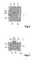
- FIG. 2 shows a first embodiment of an optical sensor 1 according to FIG. 1 in a longitudinal section.
- the printed circuit board 10, which serves in the present case for receiving the evaluation unit 9 and the transmitter 2 and the receiver 5 as optical elements, abuts the housing walls on the top and bottom of the housing 12.
- the housing 12 consists in the present case of a plastic injection molded part.
- the circuit board 10 can be moved in the direction indicated in Figure 2 x.
- the adjustment takes place by means of an actuating element, which is formed in the present case of a segment 12a of the housing 12, which is mounted in a housing wall elastic and thus adjustable.
- the elastic bearing is achieved by a thin annular web 12b, which is also part of the housing wall.
- the web 12b consists of a wall segment of the housing 12 with greatly reduced wall thickness and is therefore elastically deformable, so that by applying a contact pressure on the outside of the housing 12 on the segment 12a, the circuit board 10 can be moved in the housing 12.
- the position adjustment of the segment 12a can be done by means of a device, not shown.
- a low-pressure mass 13 is injected into the housing interior via injection channels 14, 14 '.
- the housing 12 is sealed against the ingress of moisture and dirt.
- the circuit board 10 is in its desired position fixed in position.
- In the low-pressure mass 13 is a Kunststoffinasse that is injected in the liquid state in a low-pressure injection process in the housing 12 and then solidifies on cooling.
- FIG. 3 shows a variant of the embodiment according to FIG. 2.
- the printed circuit board 10 accommodating the transmitter 2 and the receiver 5 abuts on opposite sides of the housing 12 of the optical sensor 1.
- a display element in the form of a light guide 15 is provided in the present case.
- the dome-shaped upper part of the light guide 15 is exposed on the outside of the housing 12.
- a pin-shaped part of the light guide 15 is guided through a bore 12 c in the housing 12 and coupled to the circuit board 10.
- the light guide 15 lies with clearance in the bore 12c, so that by exerting a pressure on the light guide 15 on the outside of the housing 12, the circuit board 10 can be moved in the direction indicated by x.
- the low-pressure mass 13 is in turn injected via the injection channels 14, 14 'into the interior of the housing 12 for fixing the position of the printed circuit board 10. Again, at the same time, the sealing of the housing 12 by means of the low-pressure mass 13, in particular the bore 12c.
- FIG. 4 shows a further variant of the embodiment according to FIG. 2.
- the printed circuit board 10 with the transmitter 2 and the receiver 5 in the housing 12 of the optical sensor 1 is in turn adjusted via an adjusting element.
- a pin 16 is provided in the present case, which is guided in a bore 12 c of the housing 12.
- a pressure is exerted on the pin 16 from the outside of the housing 12, whereby it is pushed into the interior space of the housing 12.
- the circuit board 10 is moved to adjust the transmitter 2 and the receiver 5.
- the pin 16 is chamfered on a front side and bears against a corresponding beveled edge of the printed circuit board 10.
- FIG. 5a shows the optical sensor 1 in a longitudinal section
- Figure 5b shows a side view of the housing 12 of the optical sensor 1.
- the transmitting optics 7 in a tube 17.
- an exit window 18 is integrated in the front wall of the housing 12.
- the tube 17 is close to the inner sides of the housing 12, so that the area of the exit window 18 is sealed with it, so that when low pressure mass 13 is injected via the injection channel 14, the low pressure mass 13 can not reach the exit window 18.
- FIG. 6 shows the optical sensor 1 according to FIGS. 5a, 5b in a spray device 19 which serves to inject the low-pressure mass 13 into the injection channel 14.
- FIG. 7 shows a further embodiment of an optical sensor 1, in which the transmitter 2 is mounted on a first printed circuit board 10 'and the receiver 5 a second circuit board 10 are arranged.
- the printed circuit boards 10, 10 ' are arranged to adjust the position of the transmitter 2 and the receiver 5.
- the transmitter 2, the receiver 5 and the associated transmission optics 7 and receiving optics 8 are integrated in a common tube.
- the low-pressure mass 13, which is injected into the housing 12, not shown in Figure 7, at the same time used as an adjusting element for positional adjustment of the circuit boards 10, 10 'and as a means for fixing the position of the circuit boards 10, 10'.
- the positional adjustment of the printed circuit boards 10, 10 ' is preferably carried out such that they are brought to this spatially remote injection channels 14, 14'.
- FIGS. 8a, b show a variant of the embodiment according to FIG. 7.
- FIG. 8a shows a longitudinal section through the optical sensor 1
- FIG. 8b shows a cross section through the optical sensor 1.
- a printed circuit board 10 for receiving the receiver 5 and the evaluation unit 9.
- the circuit board 10 slots are milled so that a circuit board 10a on the circuit board 10 coupled further printed circuit board 10 'is formed, on which the transmitter 2 is located.
- the printed circuit board webs 10a are so thin that they can be bent so that the printed circuit board 10 'can be displaced relative to the printed circuit board 10 in the direction indicated by x to adjust the transmitter 2.
- the position of the printed circuit board 10' can be selectively changed and fixed at the same time.
- the injection channels 14, 14 ' are separated by a separating web 20 as part of the housing 12.
- low-pressure mass 13 is first injected into the injection channel 14 ', whereby the printed circuit board 10' is deflected to the left for adjustment of the transmitter 2 in the intermediate plane. After the low-pressure mass 13 has cooled, the adjustment position of the transmitter 2, low-pressure mass 13, which is shown in FIG. 8 a, is also injected into the injection channel 14 for further positional fixation.
- FIGS. 9a, b show a further embodiment of an optical sensor 1.
- FIG. 9a shows a first cross section through the optical sensor 1 with a printed circuit board 10 mounted in the housing 12, on which the transmitter 2 and the receiver 5 are arranged as optical elements to be adjusted.
- FIG. 9b shows a second cross section through the optical sensor 1 with a transmitting optics 7 and a receiving optics 8, which are mounted stationarily within the housing 12.
- the circuit board 10 can be changed in position.
- the circuit board 10 is tiltably mounted with a trough-shaped recess 22 on a rocker 23 on the underside of the housing 12.
- the desired position of the printed circuit board which is indicated in FIG. 9a by tilting by ⁇ y from the horizontal, can be performed by adjusting elements, not shown, as described in the exemplary embodiments according to FIGS. 2 and 4.
- the position fixation on the printed circuit board 10 takes place in turn by injecting low-pressure mass 13 into the housing 12.
- FIG. 10 shows another embodiment of an optical sensor 1.
- a printed circuit board 10 is fixedly mounted, on which the transmitter 2 and the receiver 5 are arranged.
- openings 12d, e of the front wall of the housing 12 a transmitting optics 7 assigned to the transmitter 2 and a receiving optics 8 assigned to the receiver 5 are assigned.
- the complete assembly of the transmitting optics 7, the receiving optics 8 and the transmitter 2 and the receiver 5 is integrated in a tube 17.
- the transmitting optics 7 relative to the transmitter 2 and the receiving optics 8 relative to the receiver 5 can be placed on this an adjusting ring 24 from the outside of the housing 12 to the transmitting optics 7 and the receiving optics 8.
- FIG. 10 shows an adjusting ring 24 placed on the transmitting optics 7.
- the adjusting optics 7 and, in the same way, the receiving optics 8 in the y direction are aligned with the adjusting ring 24.
- the position fixation is in turn carried out by injecting low-pressure mass 13 into the housing 12.
- FIG. 11 shows a variant of the embodiment of the optical sensor 1 according to FIG. 10.
- the transmitter 2 and the receiver 5 are in turn arranged on a stationary printed circuit board 10 and integrated with the transmitting optics 7 and the receiving optics 8 in a tube 17.
- the transmitting optics 7 and the receiving optics 8 are stationarily mounted in the front wall of the housing 12.
- a diaphragm 11 downstream.
- An edge of the diaphragm 11 is mounted in a base 25 as part of the housing 12.
- the opposite edge of the aperture 11 is located in a slot 26 of the housing wall.
- the diaphragm 11 is displaceable in the y direction.
- a tool By means of a tool can be pressed from the outside of the housing 12 against the diaphragm 11, whereby it is displaced for adjustment in the y-direction.
- the positional fixing takes place by injecting the low-pressure mass 13 into the housing 12.
Abstract
Description
- Die Erfindung betrifft einen optischen Sensor gemäß dem Oberbegriff des Anspruchs 1.
- Derartige optische Sensoren sind typischerweise als Lichtschranken, Reflexionslichtschranken, Lichttaster, Distanzsensoren und dergleichen ausgebildet und weisen einen Sendelichtstrahlen emittierenden Sender und einen Empfangslichtstrahlen empfangenden Empfänger auf, welche in einem gemeinsamen Gehäuse oder in gesamten Gehäusen untergebracht sind. Dem Sender und Empfänger als erste Optikelemente können als weitere Optikelemente Optiken wie Linsen oder auch Blenden zugeordnet sein.
- Um eine fehlerfreie Funktion bei der Detektion von Objekten zu gewährleisten, müssen bei optischen Sensoren dieser Art einzelne Optikelemente justiert werden, um eine exakte vorgegebene Strahlführung der Sendelichtstrahlen bzw. Empfangslichtstrahlen zu erhalten.
- Zu dieser Justage wird bei optischen Sensoren typischerweise die Position eines Optikelements wie einem Sender, Empfänger oder einer diesen Elementen zugeordneten Linse, mittels einer Einstellschraube verschoben. Die Einstellung erfolgt dabei gegen die Federkraft einer Feder.
- Nachteilig hierbei ist einerseits, dass die Positionsgenauigkeit des Optikelements nur ungenügend ist. Zudem ist mit derartigen Einstellungsschrauben nur eine mangelhafte Lagefixierung des Optikelements in der eingestellten Justageposition möglich.
- Aus der
DE 299 07 270 U1 ist eine Verbindungsvorrichtung für optoeletronische Bauteile eines optischen Sensors bekannt. Die Verbindungsvorrichtung umfasst zwei korrespondierende Kopplungselemente, insbesondere eine Anordnung von Führungsstiften als ersten Kopplungselementen und eine das optoeletrische Bauteil tragenden Platte mit Bohrungen, welche in die Führungsstifte eingeführt werden. Die Platte mit dem optoelektronischen Bauteil wird manuell an den Führungsstiften ausgerichtet und dann mit einer Klebmasse oder mit Lötzinn lagefixiert. - Nachteilig bei dieser Verbindung ist, dass die Justage des optoelektronischen Bauteils nur bei geeigneten optischen Sensoren erfolgen kann. Weiterhin ist nachteilig, dass das Aufbringen der Klebmasse oder des Lötzinns einen zusätzlichen, zeitaufwendigen Fertigungsschritt bei der Herstellung des optischen Sensors bedeutet.
- Der Erfindung liegt die Aufgabe zugrunde einen optischen Sensor der eingangs genannten Art bereitzustellen, bei welchem mit konstruktiv geringem Aufwand eine genaue und reproduzierbare Justage von Optikelementen ermöglicht wird.
- Zur Lösung dieser Aufgabe sind die Merkmale des Anspruchs 1 vorgesehen. Vorteilhafte Ausführungsformen und zweckmäßige Weiterbildungen der Erfindung sind in den Unterlassungsansprüchen beschrieben.
- Der erfindungsgemäße optische Sensor dient zur Erfassung von Objekten in einem Überwachungsbereich. Er umfasst als Optikelemente wenigstens einen Sendelichtstrahlen emittierenden Sender und/oder einen Empfangslichtstrahlen empfangenden Empfänger, welche innerhalb eines Gehäuses angeordnet sind. Ein Optikelement ist durch wenigstens ein Stellelement justierbar und das justierte Optikelement ist durch eine in das Gehäuse eingespritzte Niederdruckmasse lagefixiert, wobei die Niederdruckmasse ein Dichtmittel für das Gehäuse bildet.
- Ein wesentlicher Vorteil der Erfindung besteht darin, dass die Niederdruckmasse, die zur Abdichtung des Gehäuses des optischen Sensors dient, gleichzeitig zur Lagefixierung des justierenden Optikelements dient. Damit ist zur Lagefixierung des justierenden Optikelements kein separater Fertigungsschritt notwendig, wodurch die Fertigungszeiten zur Herstellung des optischen Sensors und auch deren Herstellkosten signifikant reduziert werden können.
- Ein weiterer wesentlicher Vorteil der Erfindung besteht darin, dass die Stellelemente an der Außenseite des Gehäuses des optischen Sensors angeordnet sein können, so dass die mit den Stellelementen durchgeführte Justage bei geschlossenem Gehäuse durchführbar ist. Besonders vorteilhaft ist dabei das Stellelement in das Gehäuse integrierbar, d. h. es bildet einen Bestandteil einer Gehäusewand des Gehäuses. Damit wird die Anzahl der einzelnen Bestandteile des optischen Sensors weiter reduziert.
- Als Stellelement kann wenigstens ein Stift vorgesehen sein. Das so ausgebildete Stellelement kann auch in optischen Sensoren mit sehr kleinen Bauformen zur Justage von Optikelementen vorgesehen werden. Vorteilhaft hierbei ist insbesondere, dass durch eine geeignete Ausbildung der Spitze eines Stifts, die gegen das Optikelement geführt ist, die Verschieberichtung des Optikelements zur Durchführung der Justage vorgegeben werden kann. Besonders vorteilhaft liegt der wenigstens eine Stift in einer Bohrung in der Gehäusewand des Gehäuses, so dass mit diesem bei geschlossenem optischen Sensor an dessen Außenseite die Justage des Optikelements durchführbar ist. Dabei ist insbesondere vorteilhaft, dass durch das Einspritzen der Niederdruckmasse die den Stift aufnehmende Bohrung abgedichtet und der Stift zugleich in der Bohrung lagefixiert wird.
- In einer weiteren vorteilhaften Ausführungsform kann das Stellelement von einem in einer Gehäusewand elastisch und somit lageveränderbar gelagerten Segment gebildet sein, wobei elastische Lagerung und das Segment selbst Bestandteil des Gehäuses sind. Diese Ausführungsform zeichnet sich durch eine geringe Anzahl von Einzelteilen zur Bereitstellung der Justageanordnung für ein Optikelement aus.
- In einer weiteren vorteilhaften Ausgestaltung können Anzeigeelemente wie zum Beispiel an der Außenseite des Gehäuses sichtbar angeordnete Lichtleiter als Stellelement mitgenutzt werden. Durch die Doppelfunktion der Anzeigeelemente gelingt eine Reduktion der Einzelteile des optischen Sensors.
- In einer weiteren besonders vorteilhaften Ausgestaltung der Erfindung wird die Niederdruckmasse selbst als Stellelement zur Justage verwendet. Diese Ausführungsform zeichnet sich durch einen besonders einfachen Aufbau aus, wobei besonders vorteilhaft ist, dass keine separaten Teile zur Ausbildung des Stellelements benötigt werden. Weiterhin ist vorteilhaft, dass in diesem Fall der Justagevorgang des Optikelements und dessen Lagefixieren durch das Einspritzen der Niederdruckmasse in einem einzigen Arbeitsgang durchgeführt werden kann. Besonders vorteilhaft sind zur Justage des Optikelements auf dieses von der Außenseite des Gehäuses her mehrere räumlich zueinander abgesetzte Einspritzkanäle vorgesehen. So kann die Position des Optikelements durch die Vorgabe der Reihenfolge, in welcher die Niederdruckmasse in die Einspritzkanäle eingespritzt wird, sowie der Vorgabe des jeweiligen Einspritzdrucks, mit welchem Niederdruckmasse in einen der Einspritzkanäle eingespritzt wird, genau vorgegeben werden.
- Die Stellelemente können einerseits direkt auf die zu justierenden Optikelemente einwirken oder andererseits auf Bauteile, auf oder in welchen die Optikelemente einzeln oder in Mehrfachanordnungen angeordnet sind.
- Die Optikelemente können einerseits von dem Sender und/oder dem Empfänger des optischen Sensors gebildet sein oder andererseits von diesen zugeordneten Elementen zwei Optiken, insbesondere Linsen, Blenden oder auch einem Sendelichtleiter, dessen Position relativ zum Sender in Form eines Sonderchips ausgerichtet werden muss.
- Die Optikelemente wie ein Sender oder ein Empfänger können auf einer Leiterplatte angeordnet sein, deren Position mittels des Stellelements justierbar ist. Weiterhin kann eine Sendeoptik oder eine Empfangsoptik in Form einer Linse in einem Tubus als zu justierendes Bauteil angeordnet sein. Weiterhin kann ein Kollimator, in welchem ein Sender und eine Sendeoptik integriert sind, als zu justierendes Bauteil vorgesehen sein. Schließlich können Blenden als justierende Optikelemente vorgesehen sein.
- Die Erfindung wird im Nachstehenden anhand der Zeichnungen erläutert. Es zeigen:
- Figur 1:
- Blockschaltbild eines optischen Sensors.
- Figur 2:
- Erste Ausführungsform eines Stellelements zur Justierung eines Optikelements und optischen Sensors.
- Figur 3:
- Zweite Ausführungsform eines Stellelements zur Justierung eines Optikelements und optischen Sensors.
- Figur 4:
- Dritte Ausführungsform eines Stellelements zur Justierung eines Optikelements und optischen Sensors.
- Figur 5:
- Vierte Ausführungsform eines Stellelements zur Justierung eines Optikelements und optischen Sensors
- a) Längsschnittdarstellung
- b) Seitenansicht.
- Figur 6:
- Spritzvorrichtung für die Ausführungsform gemäß den Figuren 5a und 5b.
- Figur 7:
- Fünftes Ausführungsbeispiel zur Justierung eines Optikelements eines optischen Sensors.
- Figur 8a:
- Längsschnitt durch eine Variante des optischen Sensors gemäß Figur 7.
- Figur 8b:
- Querschnitt durch den optischen Sensor gemäß Figur 8a.
- Figur 9a:
- Letztes Ausführungsbeispiel zur Justierung eines Optikelements eines optischen Sensors.
- Figur 9b:
- Schematische Darstellung der Sende- und Empfangsoptik des optischen Sensors gemäß Figur 9a.
- Figur 10:
- Siebtes Ausführungsbeispiel zur Justierung eines Optikelements eines optischen Sensors.
- Figur 11:
- Achtes Ausführungsbeispiel zur Justierung eines Optikelements eines optischen Sensors.
- Figur 1 zeigt schematisch den Aufbau eines als Lichttaster ausgebildeten optischen Sensors 1. Der optische Sensor 1 umfasst einen Sender 2 in Form einer Leuchtdiode oder dergleichen, welcher Sendelichtstrahlen 3 emittiert. Weiterhin ist ein Empfangslichtstrahlen 4 empfangender Empfänger 5 vorgesehen, welcher von einer Photodiode oder dergleichen gebildet ist. Bei der Erfassung von Objekten 6 in einem Überwachungsbereich werden die Sendelichtstrahlen 3 zum jeweiligen Objekt 6 geführt und von dort als Empfangslichtstrahlen 4 zurück zum Empfänger 5 reflektiert. Zur Strahlformung der Sendelichtstrahlen 3 ist dem Sender 2 eine Sendeoptik 7 vorgeordnet. Mittels einer Empfangsoptik 8 erfolgt die Fokussierung der Empfangslichtstrahlen 4 auf den Empfänger 5. Aus den Empfangssignalen am Ausgang des Empfängers 5 wird in einer Auswerteeinheit 9, die von einem Mikroprozessor oder dergleichen gebildet ist, ein binäres Objektfeststellungssignal generiert, dessen Schaltzustände angeben, ob sich ein Objekt 6 im Überwachungsbereich befindet oder nicht. Das Objektfeststellungssignal wird über einen nicht dargestellten Schaltausgang ausgegeben. Im vorliegenden Ausführungsbeispiel sind der Sender 2 und der Empfänger 5 auf einer gemeinsamen Leiterplatte 10 angeordnet. Weiterhin ist dem Sender 2 zur Ausblendung eines Teils der Sendelichtstrahlen 3 eine Blende 11 nachgeordnet. Sämtliche Komponenten des optischen Sensors 1 sind in einem Gehäuse 12 angeordnet.
- Figur 2 zeigt eine erste Ausführungsform eines optischen Sensors 1 gemäß Figur 1 in einer Längsschnittdarstellung. Die Leiterplatte 10, die im vorliegenden Fall zur Aufnahme der Auswerteeinheit 9 sowie des Senders 2 und des Empfängers 5 als Optikelementen dient, liegt an den Gehäusewänden an der Ober-und Unterseite des Gehäuses 12 an. Das Gehäuse 12 besteht im vorliegenden Fall aus einem Kunststoff-Spritzteil. Zur Justierung der Optikelemente, d. h. des Senders 2 und des Empfängers 5, kann die Leiterplatte 10 in der in Figur 2 mit x bezeichneten Richtung verschoben werden. Die Justage erfolgt mittels eines Stellelements, welches im vorliegenden Fall von einem Segment 12a des Gehäuses 12 gebildet ist, welches in einer Gehäusewand elastisch und damit verstellbar gelagert ist. Die elastische Lagerung wird erzielt durch einen dünnen ringförmigen Steg 12b, der ebenfalls Bestandteil der Gehäusewand ist. Der Steg 12b besteht aus einem Wandsegment des Gehäuses 12 mit stark reduzierter Wandstärke und ist daher elastisch verformbar, so dass durch Ausüben eines Anpressdrucks an der Außenseite des Gehäuses 12 auf das Segment 12a die Leiterplatte 10 im Gehäuse 12 verschoben werden kann. Die Positionsverstellung des Segments 12a kann mittels einer nicht dargestellten Vorrichtung erfolgen. Sobald durch Andrücken gegen das Segment 12a die Leiterplatte 10 in ihrer Sollposition liegt, wird eine Niederdruckmasse 13 über Einspritzkanäle 14, 14' in den Gehäuseinnenraum eingespritzt. Mit der Niederdruckmasse 13 wird einerseits das Gehäuse 12 gegen Eindringen von Feuchtigkeit und Verschmutzungen abgedichtet. Zugleich wird auch die Leiterplatte 10 in ihrer Sollposition lagefixiert. Bei der Niederdruckmasse 13 handelt es sich um eine Kunststoffinasse, die im flüssigen Zustand in einem Niederdruckspritzvorgang in das Gehäuse 12 eingespritzt wird und dann bei Erkalten erstarrt.
- Figur 3 zeigt eine Variante der Ausführungsform gemäß Figur 2. Auch in diesem Fall liegt die den Sender 2 und den Empfänger 5 aufnehmende Leiterplatte 10 an gegenüberliegenden Seiten des Gehäuses 12 des optischen Sensors 1 an. Als Stellelement zur Justage der Leiterplatte 10 ist im vorliegenden Fall ein Anzeigeelement in Form eines Lichtleiters 15 vorgesehen. Der kuppelförmige obere Teil des Lichtleiters 15 liegt an der Außenseite des Gehäuses 12 frei. Ein stiftförmiger Teil des Lichtleiters 15 ist durch eine Bohrung 12c im Gehäuse 12 geführt und an die Leiterplatte 10 angekoppelt. Der Lichtleiter 15 liegt mit Spiel in der Bohrung 12c, so dass durch Ausüben eines Drucks auf den Lichtleiter 15 an der Außenseite des Gehäuses 12 die Leiterplatte 10 in der mit x bezeichneten Richtung verschoben werden kann. Sobald bei der so durchgeführten Justage die Leiterplatte 10 mit den Optikelementen in ihrer Sollposition liegt, wird wiederum die Niederdruckmasse 13 über die Einspritzkanäle 14, 14' in den Innenraum des Gehäuses 12 zur Lagefixierung der Leiterplatte 10 eingespritzt. Dabei erfolgt wiederum zugleich die Abdichtung des Gehäuses 12 mittels der Niederdruckmasse 13, insbesondere auch der Bohrung 12c.
- Figur 4 zeigt eine weitere Variante der Ausführungsform gemäß Figur 2. Die Leiterplatte 10 mit dem Sender 2 und dem Empfänger 5 im Gehäuse 12 des optischen Sensors 1 wird wiederum über ein Stellelement justiert. Als Stellelement ist im vorliegenden Fall ein Stift 16 vorgesehen, der in einer Bohrung 12c des Gehäuses 12 geführt ist. Mittels einer geeigneten Vorrichtung wird von der Außenseite des Gehäuses 12 ein Druck auf den Stift 16 ausgeübt, wodurch dieser in den Innraum des Gehäuses 12 geschoben wird. Dadurch wird die Leiterplatte 10 zur Justage des Senders 2 und des Empfängers 5 verschoben. Wie aus Figur 4 ersichtlich, ist der Stift 16 an einer Vorderseite abgeschrägt und liegt an einem entsprechend abgeschrägten Rand der Leiterplatte 10 an. Dadurch wird erreicht, dass bei Einschieben des Stifts in x-Richtung die Leiterplatte 10 senkrecht hierzu in y-Richtung verschoben wird. Die Fixierung der Leiterplatte 10 erfolgt wiederum durch Einspritzen von Niederdruckmasse 13 über einen Einspritzkanal 14.
- Die Figuren 5a und 5b zeigen eine erweiterte Ausführungsform eines optischen Sensors 1. Figur 5a zeigt den optischen Sensor 1 in einem Längsschnitt, Figur 5b zeigt eine Seitenansicht des Gehäuses 12 des optischen Sensors 1. In diesem Fall sind als zu justierende Optikelemente der Sender 2 und die Sendeoptik 7 in einem Tubus 17 angeordnet. In der Frontwand des Gehäuses 12 ist ein Austrittsfenster 18 integriert. Der Tubus 17 liegt an den Innenseiten des Gehäuses 12 dicht an, so dass mit dessen der Bereich des Austrittsfensters 18 abgedichtet wird, so dass bei Einspritzen von Niederdruckmasse 13 über den Einspritzkanal 14 die Niederdruckmasse 13 nicht an das Austrittsfenster 18 gelangen kann.
- Zur Justage des Senders 2 und der Sendeoptik 7 als Optikelementen wird die Position des Tubus 17 mittels zweier Stifte 16, 16' als Stellelementen eingestellt, welche wiederum in Bohrungen 12c in einer Gehäusewand geführt sind. Durch den Stift 16 wird der Tubus 17 in der x-y-Ebene gedreht. Durch den Stift 16' wird der Tubus in der x-z-Ebene gedreht. Die Lagefixierung des Tubus 17 erfolgt durch Einspritzen von Niederdruckmasse 13 in den Einspritzkanal 14. Figur 6 zeigt den optischen Sensor 1 gemäß den Figuren 5a, 5b in einer Spritzvorrichtung 19, die zum Einspritzen der Niederdruckmasse 13 in den Einspritzkanal 14 dient. Mit Schiebern 19a als Bestandteilen der Spritzvorrichtung 19 wird ein Anpressdruck auf die Stifte 16, 16' ausgeübt um die Justage des Tubus vor Einspritzen der Niederdruckmasse 13 vorzunehmen. Der Justagevorgang wird dadurch kontrolliert, dass der optische Sensor 1 innerhalb der Spritzvorrichtung liegend ein Objekt 6 als Target vermisst. Durch Beobachten des Sendelichtflecks auf dem Target wird die Güte der Justage kontrolliert.
- Figur 7 zeigt eine weitere Ausführungsform eines optischen Sensors 1, bei welchem der Sender 2 auf einer ersten Leiterplatte 10' und der Empfänger 5 auf einer zweiten Leiterplatte 10 angeordnet sind. Die Leiterplatten 10, 10' sind zur Justage des Senders 2 und des Empfängers 5 positionsverstellbar angeordnet. Der Sender 2, der Empfänger 5 sowie die diesen zugeordnete Sendeoptik 7 und Empfangsoptik 8 sind in einem gemeinsamen Tubus integriert. Im vorliegenden Fall wird die Niederdruckmasse 13, die in das in Figur 7 nicht dargestellte Gehäuse 12 eingespritzt wird, zugleich als Stellelement zur Positionsverstellung der Leiterplatten 10, 10' als auch als Mittel zur Lagefixierung der Leiterplatten 10, 10' genutzt. Die Positionsverstellung der Leiterplatten 10, 10' erfolgt bevorzugt derart, dass an diese räumlich abgesetzte Einspritzkanäle 14, 14' herangeführt sind. Durch eine geeignete Vorgabe der Reihenfolge, in welcher die Niederdruckmasse 13 in die Einspritzkanäle 14, 14' eingeführt wird, und durch die Vorgabe des Einspritzdrucks in dem jeweiligen Einspritzkanal 14, 14' kann die Positionierung der Leiterplatten 10 durchgeführt werden.
- Die Figuren 8a, b zeigen eine Variante der Ausführungsform gemäß Figur 7. Figur 8a zeigt einen Längsschnitt durch den optischen Sensor 1, Figur 8b zeigt einen Querschnitt durch den optischen Sensor 1. Im Innenraum des Gehäuses 12 liegt eine Leiterplatte 10 zur Aufnahme des Empfängers 5 und der Auswerteeinheit 9. In die Leiterplatte 10 sind Schlitze so eingefräst, dass eine über Leiterplattenstege 10a an die Leiterplatte 10 gekoppelte weitere Leiterplatte 10' gebildet wird, auf welcher der Sender 2 liegt. Die Leiterplattenstege 10a sind so dünn, dass diese gebogen werden können, so dass zur Justage des Senders 2 die Leiterplatte 10' in der mit x bezeichneten Richtung gegenüber der Leiterplatte 10 verschoben werden kann. Durch selektives Einspritzen von Niederdruckmasse 13 in die Einspritzkanäle 14, 14' kann die Position der Leiterplatte 10' gezielt verändert und zugleich fixiert werden. Wie aus Figur 8b ersichtlich, sind die Einspritzkanäle 14, 14' durch einen Trennsteg 20 als Bestandteil des Gehäuses 12 getrennt.
- Zudem sind die Zwischenräume zwischen den Leiterplatten 10, 10' durch Abdeckungen 21 abgedichtet, so dass die Niederdruckmasse 13 nicht in den Bereich des Austrittsfensters 18 gelangen kann. Wie aus Figur 8a ersichtlich, wird zuerst Niederdruckmasse 13 in den Einspritzkanal 14' eingespritzt, wodurch die Leiterplatte 10' zur Justierung des Senders 2 in der Zwischenebene nach links ausgelenkt wird. Nach Erkalten der Niederdruckmasse 13 wird zur weiteren Lagefixierung der in Figur 8a dargestellten Justageposition des Senders 2, Niederdruckmasse 13 auch in den Einspritzkanal 14 eingespritzt.
- Die Figuren 9a, b zeigen eine weitere Ausführungsform eines optischen Sensors 1. Figur 9a zeigt einen ersten Querschnitt durch den optischen Sensor 1 mit einer im Gehäuse 12 gelagerten Leiterplatte 10, auf welcher als zu justierende Optikelemente der Sender 2 und der Empfänger 5 angeordnet sind.
- Figur 9b zeigt einen zweiten Querschnitt durch den optischen Sensor 1 mit einer Sendeoptik 7 und einer Empfangsoptik 8, welche stationär innerhalb des Gehäuses 12 gelagert sind. Zur Ausrichtung des Senders 2 relativ zur Sendeoptik 7 und zur Ausrichtung der Empfangsoptik 8 relativ zum Empfänger 5, kann die Leiterplatte 10 in ihrer Position verändert werden. Hierzu ist die Leiterplatte 10 mit einer muldenförmigen Aussparung 22 auf einer Wippe 23 an der Unterseite des Gehäuses 12 kippbar gelagert. Die Sollposition der Leiterplatte, die in Figur 9a durch ein Verkippen um Δ y aus der Horizontalen angedeutet ist, kann durch nicht dargestellte Stellelemente, wie sie in den Ausführungsbeispielen gemäß den Figuren 2 und 4 beschrieben sind, vorgenommen werden. Die Lagefixierung an der Leiterplatte 10 erfolgt wiederum durch Einspritzen von Niederdruckmasse 13 in das Gehäuse 12.
- Figur 10 zeigt ein weiteres Ausführungsbeispiel eines optischen Sensors 1. Im Gehäuse 12 des optischen Sensors 1 ist eine Leiterplatte 10 ortsfest gelagert, auf welcher der Sender 2 und der Empfänger 5 angeordnet sind. In Öffnungen 12d, e der Frontwand des Gehäuses 12 sind eine dem Sender 2 zugeordnete Sendeoptik 7 und eine dem Empfänger 5 zugeordnete Empfangsoptik 8 zugeordnet. Die komplette Baueinheit der Sendeoptik 7, der Empfangsoptik 8 sowie dem Sender 2 und dem Empfänger 5 ist in einem Tubus 17 integriert. Zur Justage der Sendeoptik 7 relativ zum Sender 2 und der Empfangsoptik 8 relativ zum Empfänger 5 kann auf diese ein Justierring 24 von der Außenseite des Gehäuses 12 auf die Sendeoptik 7 bzw. auf die Empfangsoptik 8 aufsetzt werden. Figur 10 zeigt einen auf die Sendeoptik 7 aufgesetzten Justierring 24. Mit dem Justierring 24 wird die Sendeoptik 7 und in gleicher Weise auch die Empfangsoptik 8 in y-Richtung ausgerichtet. Die Lagefixierung erfolgt wiederum durch Einspritzen von Niederdruckmasse 13 in das Gehäuse 12.
- Figur 11 zeigt eine Variante der Ausführungsform des optischen Sensors 1 gemäß Figur 10. Der Sender 2 und der Empfänger 5 sind wiederum auf einer ortsfest angeordneten Leiterplatte 10 angeordnet und mit der Sendeoptik 7 und der Empfangsoptik 8 in einem Tubus 17 integriert. Im Unterschied zur Ausführungsform gemäß Figur 10 sind bei dem optischen Sensor 1 gemäß Figur 11 die Sendeoptik 7 und die Empfangsoptik 8 ortsfest in der Frontwand des Gehäuses 12 gelagert. Als zu justierendes Optikelement ist dem Sender 2 im vorliegenden Fall eine Blende 11 nachgeordnet. Ein Rand der Blende 11 ist in einem Sockel 25 als Bestandteil des Gehäuses 12 gelagert. Der gegenüberliegende Rand der Blende 11 liegt in einem Schlitz 26 der Gehäusewand. Dadurch ist die Blende 11 in y-Richtung verschiebbar. Mittels eines Werkzeugs kann von der Außenseite des Gehäuses 12 gegen die Blende 11 gedrückt werden, wodurch diese zur Justage in y-Richtung verschoben wird. Sobald die Blende 11 in ihrer Sollposition liegt, erfolgt deren Lagefixierung durch Einspritzen der Niederdruckmasse 13 in das Gehäuse 12.
-
- (1)
- Optischer Sensor
- (2)
- Sender
- (3)
- Sendelichtstrahlen
- (4)
- Empfangslichtstrahlen
- (5)
- Empfänger
- (6)
- Objekt
- (7)
- Sendeoptik
- (8)
- Empfangsoptik
- (9)
- Auswerteeinheit
- (10)
- Leiterplatte
- (10')
- Leiterplatte
- (10a)
- Leiterplattensteg
- (11)
- Blende
- (12)
- Gehäuse
- (12a)
- Segment
- (12b)
- Steg
- (12c)
- Bohrung
- (12d)
- Öffnung
- (12e)
- Öffnung
- (13)
- Niederdruckmasse
- (14)
- Einspritzkanal
- (14')
- Einspritzkanal
- (15)
- Lichtleiter
- (16)
- Stifte
- (16')
- Stifte
- (17)
- Tubus
- (18)
- Austrittsfenster
- (19)
- Spritzvorrichtung
- (19a)
- Schieber
- (20)
- Trennsteg
- (21)
- Abdeckung
- (22)
- Aussparung
- (23)
- Wippe
- (24)
- Justierung
- (25)
- Sockel
- (26)
- Schlitz
Claims (22)
- Optischer Sensor zur Erfassung von Objekten in einem Überwachungsbereich, mit Optikelementen umfassend wenigstens einen Sendelichtstrahlen emittierenden Sender und/oder einen Empfangslichtstrahlen empfangenden Empfänger, welche innerhalb eines Gehäuses angeordnet sind, dadurch gekennzeichnet, dass wenigstens ein Optikelement durch wenigstens ein Stellelement justierbar ist, und dass das justierte Optikelement durch eine in das Gehäuse (12) eingespritzte Niederdruckmasse (13) lagefixiert ist, wobei die Niederdruckmasse (13) ein Dichtmittel für das Gehäuse (12) bildet.
- Optischer Sensor nach Anspruch 1, dadurch gekennzeichnet, dass das Stellelement von der Niederdruckmasse (13) gebildet ist.
- Optischer Sensor nach einem der Ansprüche 1 oder 2, dadurch gekennzeichnet, dass zur Ausbildung des Stellelements die Niederdruckmasse (13) durch Einspritzkanäle (14, 14') zu dem zu justierenden Optikelement oder einem das Optikelement aufnehmenden Bauelement geführt ist.
- Optischer Sensor nach Anspruch 3, dadurch gekennzeichnet, dass die Justageposition des Optikelements durch Vorgabe der Reihenfolge des Einspritzens von Niederdruckmasse (13) in die einzelnen Einspritzkanälen (14, 14') und/oder durch Vorgabe des Einspritzdrucks, mit welchem Niederdruckmasse (13) in einen Einspritzkanal (14, 14') einspritzbar ist, bestimmbar ist.
- Optischer Sensor nach Anspruch 1, dadurch gekennzeichnet, dass das Stellelement von einem elastisch gelagerten Segment (12a) einer Gehäusewand des Gehäuses (12) gebildet ist.
- Optischer Sensor nach Anspruch 5, dadurch gekennzeichnet, dass das Segment (12a) über elastisch verformbare Stege (12b) mit dem Grundkörper der Gehäusewand verbunden ist.
- Optischer Sensor nach Anspruch 6, dadurch gekennzeichnet, dass die Stege (12b) Bestandteil der Gehäusewand sind.
- Optischer Sensor nach Anspruch 1, dadurch gekennzeichnet, dass als Stellelement wenigstens ein Stift (16, 16') vorgesehen ist.
- Optischer Sensor nach Anspruch 8, dadurch gekennzeichnet, dass der oder jeder Stift (16, 16') von der Außenseite des Gehäuses (12) betätigbar ist.
- Optischer Sensor nach einem der Ansprüche 8 oder 9, dadurch gekennzeichnet, dass der oder jeder Stift (16, 16') in einer Bohrung (12c) einer Gehäusewand des Gehäuses (12) geführt ist.
- Optischer Sensor nach einem der Ansprüche 8 bis 10, dadurch gekennzeichnet, dass der oder jeder Stift (16, 16') in dessen Längsrichtung verschiebbar ist.
- Optischer Sensor nach Anspruch 11, dadurch gekennzeichnet, dass das Optikelement mittels eines Stifts (16) in Verschieberichtung des Stifts (16) verschiebbar ist.
- Optischer Sensor nach Anspruch 11, dadurch gekennzeichnet, dass das Optikelement mittels eines Stifts (16) quer zur Verschieberichtung des Stifts (16) verschiebbar ist.
- Optischer Sensor nach Anspruch 13, dadurch gekennzeichnet, dass die Spitze des Stifts (16) eine Abschrägung aufweist.
- Optischer Sensor nach Anspruch 1, dadurch gekennzeichnet, dass das Stellelement von einem mit dem Optikelement verbundenen Anzeigeelement gebildet ist, welche an der Außenseite des Gehäuses sichtbar installierbar ist.
- Optischer Sensor nach Anspruch 15, dadurch gekennzeichnet, dass das Anzeigeelement von einem Lichtleiter (15) gebildet ist, wobei ein stiftförmiger Teil des Lichtleiters (15) mit Spiel in einer Bohrung (12c) in einer Gehäusewand verschiebbar gelagert ist.
- Optischer Sensor nach Anspruch 16, dadurch gekennzeichnet, dass zur Lagefixierung des Lichtleiters (15) die Bohrung (12c) mit Niederdruckmasse (13) befüllbar ist.
- Optischer Sensor nach einem der Ansprüche 1 bis 17, dadurch gekennzeichnet, dass der Sender (2) und/oder der Empfänger (5) als Optikelement auf einer Leiterplatte (10) angeordnet ist, wobei mittels des Stellelements die Position der Leiterplatte (10) justierbar ist.
- Optischer Sensor nach einem der Ansprüche 1 bis 17, dadurch gekennzeichnet, dass als Optikelement eine Sendeoptik (7) oder eine Empfangsoptik (8) in einem Tubus (17) gelagert ist, dessen Position mittels eines Stellelements justierbar ist.
- Optischer Sensor nach einem der Ansprüche 1 bis 17, dadurch gekennzeichnet, dass der Sender (2) und eine Sendeoptik (7) als Optikelement in einem Kollimator integriert sind, dessen Position mittels eines Stellelements justierbar ist.
- Optischer Sensor nach einem der Ansprüche 1 bis 17, dadurch gekennzeichnet, dass als Optikelement eine Blende (11) dem Sender (2) oder Empfänger (5) zugeordnet ist, dessen Position mittels eines Stellelements justierbar ist.
- Optischer Sensor nach einem der Ansprüche 1 bis 17, dadurch gekennzeichnet, dass mittels eines Stellelements die Position eines Sendelichtleiters bezüglich des Senders (2) justierbar ist.
Applications Claiming Priority (1)
| Application Number | Priority Date | Filing Date | Title |
|---|---|---|---|
| DE200610016913 DE102006016913B4 (de) | 2006-04-11 | 2006-04-11 | Optischer Sensor |
Publications (2)
| Publication Number | Publication Date |
|---|---|
| EP1845401A1 true EP1845401A1 (de) | 2007-10-17 |
| EP1845401B1 EP1845401B1 (de) | 2011-09-28 |
Family
ID=38197923
Family Applications (1)
| Application Number | Title | Priority Date | Filing Date |
|---|---|---|---|
| EP20070005355 Not-in-force EP1845401B1 (de) | 2006-04-11 | 2007-03-15 | Verfahren zur Justage wenigstens eines Optikelementes eines optischen Sensors |
Country Status (2)
| Country | Link |
|---|---|
| EP (1) | EP1845401B1 (de) |
| DE (1) | DE102006016913B4 (de) |
Cited By (4)
| Publication number | Priority date | Publication date | Assignee | Title |
|---|---|---|---|---|
| EP2101196A1 (de) | 2008-03-14 | 2009-09-16 | Leuze electronic GmbH + Co KG | Optischer Sensor mit Lichtkonzentrator |
| CN101825764A (zh) * | 2009-03-07 | 2010-09-08 | 洛伊策电子两合公司 | 光学传感器 |
| EP2728378A1 (de) * | 2012-10-30 | 2014-05-07 | Omron Corporation | Optischer Sensor |
| EP4009225A1 (de) * | 2020-12-07 | 2022-06-08 | Leuze electronic GmbH + Co. KG | Optischer sensor |
Families Citing this family (4)
| Publication number | Priority date | Publication date | Assignee | Title |
|---|---|---|---|---|
| EP2192420A1 (de) | 2008-11-28 | 2010-06-02 | Siemens Aktiengesellschaft | Optische Sende- und Empfangs-Baueinheit und Sensor mit einer solchen |
| DE102019204613A1 (de) * | 2019-04-01 | 2020-10-01 | Micro-Epsilon Optronic Gmbh | Messsystem zur optischen Messung |
| DE102019119631A1 (de) * | 2019-07-19 | 2021-01-21 | Endress+Hauser Conducta Gmbh+Co. Kg | Verfahren zur Herstellung einer optischen Baugruppe und optische Baugruppe |
| EP4016009B1 (de) * | 2020-12-17 | 2023-10-25 | Leuze electronic GmbH + Co. KG | Optischer sensor |
Citations (10)
| Publication number | Priority date | Publication date | Assignee | Title |
|---|---|---|---|---|
| DE29907270U1 (de) | 1999-04-23 | 1999-07-29 | Sick Ag | Verbindungsvorrichtung |
| US20020075916A1 (en) * | 2000-12-06 | 2002-06-20 | Wataru Sato | Laser device and lens position adjustment method in the laser device |
| US20040016873A1 (en) * | 2002-07-25 | 2004-01-29 | Matsushita Electric Works, Ltd. | Photoelectric device-part |
| US20040075917A1 (en) * | 2002-06-28 | 2004-04-22 | Kabushiki Kaisha Toshiba | Optical module apparatus, projection television and method of fabricating optical module apparatus |
| US20040080642A1 (en) * | 2002-09-27 | 2004-04-29 | Kenichi Kobayashi | Camera module |
| US20050013562A1 (en) * | 2003-07-17 | 2005-01-20 | Naoki Tatehata | Optical component and manufacture method of the same |
| DE10326848B4 (de) | 2003-06-14 | 2005-06-23 | Leuze Lumiflex Gmbh + Co. Kg | Optischer Sensor |
| US20050199792A1 (en) | 2004-03-11 | 2005-09-15 | Leuze Electronic Gmbh & Co. Kg | Optical sensor |
| EP1610154A1 (de) * | 2004-06-25 | 2005-12-28 | Leuze electronic GmbH + Co KG | Optischer Sensor |
| EP1731926A2 (de) * | 2005-06-09 | 2006-12-13 | Leuze electronic GmbH + Co. KG | Sensor zur Erfassung von Objekten in einem Überwachungsbereich |
Family Cites Families (5)
| Publication number | Priority date | Publication date | Assignee | Title |
|---|---|---|---|---|
| DE4408294A1 (de) * | 1994-03-11 | 1995-09-21 | Sick Optik Elektronik Erwin | Vorrichtung zur Veränderung des wirksamen Strahlquerschnittprofils von optoelektronischen Sensoren |
| DE29724515U1 (de) * | 1997-01-09 | 2001-09-13 | Leuze Electronic Gmbh & Co | Befestigungsvorrichtung |
| DE19907548C2 (de) * | 1998-03-17 | 2003-08-14 | Leuze Electronic Gmbh & Co | Optoelektronische Vorrichtung |
| DE19934870C1 (de) * | 1999-07-24 | 2001-01-18 | Leuze Electronic Gmbh & Co | Befestigungsvorrichtung |
| DE102004011804A1 (de) * | 2004-03-11 | 2005-10-06 | Leuze Electronic Gmbh & Co Kg | Optischer Sensor |
-
2006
- 2006-04-11 DE DE200610016913 patent/DE102006016913B4/de not_active Expired - Fee Related
-
2007
- 2007-03-15 EP EP20070005355 patent/EP1845401B1/de not_active Not-in-force
Patent Citations (10)
| Publication number | Priority date | Publication date | Assignee | Title |
|---|---|---|---|---|
| DE29907270U1 (de) | 1999-04-23 | 1999-07-29 | Sick Ag | Verbindungsvorrichtung |
| US20020075916A1 (en) * | 2000-12-06 | 2002-06-20 | Wataru Sato | Laser device and lens position adjustment method in the laser device |
| US20040075917A1 (en) * | 2002-06-28 | 2004-04-22 | Kabushiki Kaisha Toshiba | Optical module apparatus, projection television and method of fabricating optical module apparatus |
| US20040016873A1 (en) * | 2002-07-25 | 2004-01-29 | Matsushita Electric Works, Ltd. | Photoelectric device-part |
| US20040080642A1 (en) * | 2002-09-27 | 2004-04-29 | Kenichi Kobayashi | Camera module |
| DE10326848B4 (de) | 2003-06-14 | 2005-06-23 | Leuze Lumiflex Gmbh + Co. Kg | Optischer Sensor |
| US20050013562A1 (en) * | 2003-07-17 | 2005-01-20 | Naoki Tatehata | Optical component and manufacture method of the same |
| US20050199792A1 (en) | 2004-03-11 | 2005-09-15 | Leuze Electronic Gmbh & Co. Kg | Optical sensor |
| EP1610154A1 (de) * | 2004-06-25 | 2005-12-28 | Leuze electronic GmbH + Co KG | Optischer Sensor |
| EP1731926A2 (de) * | 2005-06-09 | 2006-12-13 | Leuze electronic GmbH + Co. KG | Sensor zur Erfassung von Objekten in einem Überwachungsbereich |
Cited By (8)
| Publication number | Priority date | Publication date | Assignee | Title |
|---|---|---|---|---|
| EP2101196A1 (de) | 2008-03-14 | 2009-09-16 | Leuze electronic GmbH + Co KG | Optischer Sensor mit Lichtkonzentrator |
| CN101825764A (zh) * | 2009-03-07 | 2010-09-08 | 洛伊策电子两合公司 | 光学传感器 |
| EP2226654A3 (de) * | 2009-03-07 | 2013-02-13 | Leuze electronic GmbH + Co. KG | Optischer Sensor |
| CN101825764B (zh) * | 2009-03-07 | 2014-08-13 | 洛伊策电子两合公司 | 光学传感器 |
| EP2728378A1 (de) * | 2012-10-30 | 2014-05-07 | Omron Corporation | Optischer Sensor |
| US9448106B2 (en) | 2012-10-30 | 2016-09-20 | Omron Corporation | Optical sensor |
| US9593980B2 (en) | 2012-10-30 | 2017-03-14 | Omron Corporation | Optical sensor |
| EP4009225A1 (de) * | 2020-12-07 | 2022-06-08 | Leuze electronic GmbH + Co. KG | Optischer sensor |
Also Published As
| Publication number | Publication date |
|---|---|
| DE102006016913B4 (de) | 2008-10-09 |
| EP1845401B1 (de) | 2011-09-28 |
| DE102006016913A1 (de) | 2007-10-25 |
Similar Documents
| Publication | Publication Date | Title |
|---|---|---|
| EP1845401A1 (de) | Optischer Sensor | |
| EP0857980B1 (de) | Entfernungsmesser | |
| EP2312919B1 (de) | Optoelektronischer Sensor | |
| DE3513475C2 (de) | ||
| DE102005041998B4 (de) | Verfahren zur Justage eines abbildenden Elements sowie Messgerät justiert nach einem derartigen Verfahren | |
| EP1715313B1 (de) | Lichtkontrasttaster zur Erkennung von Marken | |
| EP1031026B1 (de) | Vorrichtung zur lageerfassung von bauelementen , lichtumlenkkörper und bestückkopf mit einer vorrichtung zur lageerfassung von bauelementen | |
| EP2023164B1 (de) | Optischer Sensor | |
| EP0735501A2 (de) | Farbsensoranordnung zum Lesen farbiger Markierungen | |
| EP1980878A1 (de) | Optoelektronischer Sensor mit verbundener Doppellinse und Herstellungsverfahren hierfür | |
| EP3324218B1 (de) | Mehrstrahllichtschranke | |
| EP1359450B1 (de) | Optischer Sensor mit justierbarer Linsenfassung | |
| DE4142108C2 (de) | Montagestruktur für ein optisches Bauteil einer Optikeinrichtung | |
| DE10009493A1 (de) | Scanner | |
| EP1651981B1 (de) | Vorrichtung zum justieren eines optischen spiegels | |
| DE102005002874B3 (de) | Optoelektronisches Bauelement mit integrierter Wellenleiter-Ankopplung für passive Justage | |
| EP3454095A1 (de) | Optoelektronisches sensorsystem | |
| EP4016009B1 (de) | Optischer sensor | |
| EP3974878B1 (de) | Linsenmodul | |
| DE202016106394U1 (de) | Mehrstrahllichtschranke | |
| DE102022214346B3 (de) | Laservorrichtung und Verfahren zu deren Montage | |
| DE102007055497A1 (de) | Optischer Sensor für ein Kraftfahrzeug | |
| EP2192420A1 (de) | Optische Sende- und Empfangs-Baueinheit und Sensor mit einer solchen | |
| DE4312490B4 (de) | Tubus für ein Varioobjektiv mit Brennweitenerfassung | |
| DE102008028970B4 (de) | Verfahren zur Ausrichtung eines optischen Sensors |
Legal Events
| Date | Code | Title | Description |
|---|---|---|---|
| PUAI | Public reference made under article 153(3) epc to a published international application that has entered the european phase |
Free format text: ORIGINAL CODE: 0009012 |
|
| 17P | Request for examination filed |
Effective date: 20070803 |
|
| AK | Designated contracting states |
Kind code of ref document: A1 Designated state(s): AT BE BG CH CY CZ DE DK EE ES FI FR GB GR HU IE IS IT LI LT LU LV MC MT NL PL PT RO SE SI SK TR |
|
| AX | Request for extension of the european patent |
Extension state: AL BA HR MK YU |
|
| 17Q | First examination report despatched |
Effective date: 20071122 |
|
| AKX | Designation fees paid |
Designated state(s): AT BE BG CH CY CZ DE DK EE ES FI FR GB GR HU IE IS IT LI LT LU LV MC MT NL PL PT RO SE SI SK TR |
|
| GRAP | Despatch of communication of intention to grant a patent |
Free format text: ORIGINAL CODE: EPIDOSNIGR1 |
|
| RTI1 | Title (correction) |
Free format text: METHOD OF ADJUSTING AT LEAST ONE OPTICAL ELEMENT OF A SENSOR |
|
| GRAS | Grant fee paid |
Free format text: ORIGINAL CODE: EPIDOSNIGR3 |
|
| GRAA | (expected) grant |
Free format text: ORIGINAL CODE: 0009210 |
|
| RBV | Designated contracting states (corrected) |
Designated state(s): BE CH DE FR GB IT LI NL |
|
| AK | Designated contracting states |
Kind code of ref document: B1 Designated state(s): BE CH DE FR GB IT LI NL |
|
| REG | Reference to a national code |
Ref country code: GB Ref legal event code: FG4D Free format text: NOT ENGLISH |
|
| REG | Reference to a national code |
Ref country code: CH Ref legal event code: EP Ref country code: CH Ref legal event code: NV Representative=s name: ROTTMANN, ZIMMERMANN + PARTNER AG |
|
| REG | Reference to a national code |
Ref country code: NL Ref legal event code: T3 |
|
| REG | Reference to a national code |
Ref country code: DE Ref legal event code: R096 Ref document number: 502007008234 Country of ref document: DE Effective date: 20111124 |
|
| PLBE | No opposition filed within time limit |
Free format text: ORIGINAL CODE: 0009261 |
|
| STAA | Information on the status of an ep patent application or granted ep patent |
Free format text: STATUS: NO OPPOSITION FILED WITHIN TIME LIMIT |
|
| 26N | No opposition filed |
Effective date: 20120629 |
|
| REG | Reference to a national code |
Ref country code: DE Ref legal event code: R097 Ref document number: 502007008234 Country of ref document: DE Effective date: 20120629 |
|
| PGFP | Annual fee paid to national office [announced via postgrant information from national office to epo] |
Ref country code: DE Payment date: 20130413 Year of fee payment: 7 |
|
| PGFP | Annual fee paid to national office [announced via postgrant information from national office to epo] |
Ref country code: CH Payment date: 20140319 Year of fee payment: 8 Ref country code: NL Payment date: 20140319 Year of fee payment: 8 |
|
| PGFP | Annual fee paid to national office [announced via postgrant information from national office to epo] |
Ref country code: IT Payment date: 20140324 Year of fee payment: 8 Ref country code: FR Payment date: 20140319 Year of fee payment: 8 |
|
| PGFP | Annual fee paid to national office [announced via postgrant information from national office to epo] |
Ref country code: GB Payment date: 20140319 Year of fee payment: 8 |
|
| PGFP | Annual fee paid to national office [announced via postgrant information from national office to epo] |
Ref country code: BE Payment date: 20140319 Year of fee payment: 8 |
|
| REG | Reference to a national code |
Ref country code: DE Ref legal event code: R119 Ref document number: 502007008234 Country of ref document: DE |
|
| REG | Reference to a national code |
Ref country code: DE Ref legal event code: R119 Ref document number: 502007008234 Country of ref document: DE Effective date: 20141001 |
|
| PG25 | Lapsed in a contracting state [announced via postgrant information from national office to epo] |
Ref country code: DE Free format text: LAPSE BECAUSE OF NON-PAYMENT OF DUE FEES Effective date: 20141001 |
|
| REG | Reference to a national code |
Ref country code: CH Ref legal event code: PL |
|
| GBPC | Gb: european patent ceased through non-payment of renewal fee |
Effective date: 20150315 |
|
| REG | Reference to a national code |
Ref country code: NL Ref legal event code: MM Effective date: 20150401 |
|
| PG25 | Lapsed in a contracting state [announced via postgrant information from national office to epo] |
Ref country code: IT Free format text: LAPSE BECAUSE OF NON-PAYMENT OF DUE FEES Effective date: 20150315 |
|
| REG | Reference to a national code |
Ref country code: FR Ref legal event code: ST Effective date: 20151130 |
|
| PG25 | Lapsed in a contracting state [announced via postgrant information from national office to epo] |
Ref country code: CH Free format text: LAPSE BECAUSE OF NON-PAYMENT OF DUE FEES Effective date: 20150331 Ref country code: LI Free format text: LAPSE BECAUSE OF NON-PAYMENT OF DUE FEES Effective date: 20150331 Ref country code: GB Free format text: LAPSE BECAUSE OF NON-PAYMENT OF DUE FEES Effective date: 20150315 |
|
| PG25 | Lapsed in a contracting state [announced via postgrant information from national office to epo] |
Ref country code: FR Free format text: LAPSE BECAUSE OF NON-PAYMENT OF DUE FEES Effective date: 20150331 |
|
| PG25 | Lapsed in a contracting state [announced via postgrant information from national office to epo] |
Ref country code: NL Free format text: LAPSE BECAUSE OF NON-PAYMENT OF DUE FEES Effective date: 20150401 |
|
| PG25 | Lapsed in a contracting state [announced via postgrant information from national office to epo] |
Ref country code: BE Free format text: LAPSE BECAUSE OF NON-PAYMENT OF DUE FEES Effective date: 20150331 |