EP1841066A1 - Einschätzung des Jitters eines Taktsignals - Google Patents
Einschätzung des Jitters eines Taktsignals Download PDFInfo
- Publication number
- EP1841066A1 EP1841066A1 EP07105026A EP07105026A EP1841066A1 EP 1841066 A1 EP1841066 A1 EP 1841066A1 EP 07105026 A EP07105026 A EP 07105026A EP 07105026 A EP07105026 A EP 07105026A EP 1841066 A1 EP1841066 A1 EP 1841066A1
- Authority
- EP
- European Patent Office
- Prior art keywords
- signal
- word
- shift register
- respect
- jitter
- Prior art date
- Legal status (The legal status is an assumption and is not a legal conclusion. Google has not performed a legal analysis and makes no representation as to the accuracy of the status listed.)
- Granted
Links
Images


Classifications
-
- G—PHYSICS
- G01—MEASURING; TESTING
- G01R—MEASURING ELECTRIC VARIABLES; MEASURING MAGNETIC VARIABLES
- G01R31/00—Arrangements for testing electric properties; Arrangements for locating electric faults; Arrangements for electrical testing characterised by what is being tested not provided for elsewhere
- G01R31/28—Testing of electronic circuits, e.g. by signal tracer
- G01R31/317—Testing of digital circuits
- G01R31/31708—Analysis of signal quality
- G01R31/31709—Jitter measurements; Jitter generators
Definitions
- the present invention generally relates to electronic circuits and, more particularly, to circuits comprising elements for generating one or more periodic signals.
- An exemplary application of the present invention relates to integrated processors comprising a clock signal generating circuit from a reference clock.
- the invention more particularly relates to the synchronization test of a clock signal generated internally by an electronic circuit with respect to an internal or external reference clock.
- FIG. 1 very schematically and partially shows an example of an electronic circuit 1 of the type to which the present invention applies.
- a circuit comprises multiple functions not shown (particularly if it is a processor) and at least one circuit 11 (PLL), for example of the phase-locked loop type, for generating at least one signal internal clock CKint from a clock signal CLK for example external.
- PLL phase-locked loop type
- a problem present in electronic circuits controlled from clock or counting signals is to ensure that these signals follow an expected value, that is to say do not undergo jitter with respect to the signal from which they are generated and more generally with respect to a reference signal.
- FIG. 2 illustrates, by a timing diagram, an example of a jitter phenomenon of a signal CKint whose real period Tr is slightly greater than an expected period T0.
- the offset ⁇ t between the two periods generates a desynchronization of the clock CKint which may cause functional problems of the circuit.
- Such noise or phase jitter is increasingly critical with increasing signal frequency, as computational results (for example, of a counter) drift rapidly relative to an expected value.
- a first method for testing the drift of a clock signal is to take the signal generated by the circuit and to measure, with an external equipment, a possible deviation from a reference signal. Such a method remains accessible for relatively low frequencies (a few hundred kilohertz) but can no longer be used for high frequencies (several megahertz, even hundreds or thousands of megahertz) because the noise added by the external measuring elements and the connectors to the point of measurement can no longer be neglected.
- a second method is to integrate, in the circuit to be tested, a device providing information relating to the phase shift of the internal clock signal relative to a reference clock to allow external exploitation of the results.
- FIG 3 shows, very schematically and in block form, a conventional example of such a device.
- This device consists of a a shift register 21 based on flip-flops D, a data input of which receives the output (for example, non-inverted Q) of a sampling flip-flop 22.
- the data input D of the flip-flop 22 receives the clock signal internal CKint to test.
- the latch 22 and the shift register 21 receive, on their respective clock inputs, a signal CKref constituting a reference clock of a frequency of the same order of magnitude as the signal to be measured.
- the n outputs Q1 to Qn of the shift register 21 are provided outside the circuit 1 to a measurement operating system 25 (for example, a microcomputer).
- the role of the shift register 21 is to parallelise the successive information on the clock fronts and their possible offset, so as to provide exploitable information despite the high frequency.
- a disadvantage of this second method is that it is necessary to load the data provided by the shift register 21 into an external system in order to be able to exploit these data and to determine any jitter between the two clock signals.
- such a device is limited to the characterization of the product and does not allow a test of a possible clock jitter of a product manufactured, for example, in a final test before possible decision of scrapping a product, or in the life of the product.
- the present invention aims to overcome all or part of the disadvantages of known clock jitter test systems.
- the invention aims more particularly at providing a circuit for estimating the possible jitter of a clock signal generated by an electronic circuit with respect to a reference signal.
- the invention also aims to propose a solution compatible with integration of the test circuit in the electronic circuit itself.
- the invention also aims to propose a solution compatible with the implementation of a product test individually after manufacture.
- the number of occurrences is compared to a threshold and is periodically reset, the jitter being considered acceptable as long as this threshold is not reached.
- the first and last bits of the reference word are identical, the second bit of this word being in a reverse state.
- the reference word comprises between one and three first bits in a first state, between one and three subsequent bits in a second state inverse to the first state and between one and three last bits in the first state.
- the current word supplied by the shift register is compared with a second reference word that is inverse to the first one.
- the measurement period is chosen as a function of the period of the reference clock.
- the number of bits of the reference word is between four and twelve, preferably between five and seven.
- the current word is formed of all the outputs of the shift register.
- the current word is formed of only part of the outputs of the shift register.
- the present invention originates from a new analysis of the jitter phenomenon of a clock with respect to a reference clock and, more particularly, from a statistical evaluation of the states of the clock signal measured with respect to the clock. reference.
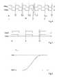
- FIG. 4 illustrates, by timing diagrams representing an example of the time course of a signal CKint to be measured with respect to a reference signal CKref, an example of phase jitter between two periodic signals. Assuming that the synchronous signals at a time t 0 , the phase shift of the signal CKint with respect to the signal CKref increases successively by the same value ⁇ t at each clock period until the two signals become synchronous at a time t n + 1 , after n + 1 periods of the reference clock signal, the signal to be measured having, during this beat time TB, only n periods.
- FIG. 4 illustrates the possibility of estimating the synchronism defect of a high frequency clock signal from a measurement at a lower frequency (period TB) by exploiting the fact that, even with jitter, the signals Periodically have common fronts.
- the signal fronts are assumed to be instantaneous. In practice, they follow a slope between the two high and low states and vice versa. This does not change the principles of the invention.
- FIG. 5 shows an enlargement of the timing diagrams of Figure 4 around the time t 0 .
- This figure illustrates that, if the phase shift is + ⁇ t in the period following the synchronous instant t 0 of the two signals, this phase shift is - ⁇ t to the preceding period. Therefore, we can consider that by comparing the respective states of the two signals (or by combining them with an AND), the synchronized edges of the two signals are, whatever the importance of the jitter, framed by specific states and inverse of each other.
- FIG. 6 represents, as a function of time t, the cumulative probability density P of a comparison of the states clock signals as a function of time. Since the probability of obtaining a state 0 or a state 1 by comparing two non-synchronous signals follows a Gaussian, this results in an S-shaped cumulative distribution between instants where one is sure to obtain a state 0 (phase shift in one direction) or a state 1 (phase shift in the other direction). The notion of state 0 or 1 is understood by comparing the two signals at sampling times.
- the invention takes advantage of this distribution to consider that the states surrounding aligned edges of the signals to be compared are out of this distribution and therefore have specific states (respectively, 0 and 1).
- the invention then provides for comparing a word contained in a shift register (parallel outputs of a series of flip-flops), driven by a reference signal and whose data input receives the sampled signal to be measured, to a word whose the first two bits or two first groups of bits have states inverted with respect to each other and whose last bit or group of bits has a state identical to that of the first bit.
- the invention provides a reference pattern for estimating the jitter of the generated signal with respect to a reference signal. This pattern is compared to the words successively present on the outputs of the shift register and the frequency of its appearance provides an estimate of the jitter of the clock signal to be measured with respect to the reference signal.
- the invention also takes advantage of the fact that to qualify a product in terms of clock jitter, it is usually sufficient that its jitter is less than a threshold. It is therefore not necessary to calculate it precisely and its estimate in relation to a threshold is sufficient.
- FIG. 7 very schematically shows in the form of blocks an embodiment of a circuit for estimating the jitter of a signal CKint generated by an electronic circuit with respect to a reference signal CKref, the signals to measure and reference being preferably alike frequency order of magnitude.
- the signal CKint is sampled by at least a first flip-flop 32 and preferably by two flip-flops 32 and 33 in series, the data input D of the flip-flop 33 being connected to the output Q of the flip-flop 32.
- the signal CKref is applied on the clock inputs of the flip-flops 32 and 33.
- a double sampling reduces the uncertainties related to set-time and hold-time of the flip-flops and to the slopes of the edges of the signals CKint and CKref.
- a shift register 31 preferably consists of D flip-flops in series whose respective outputs Q1 to Qn are provided in parallel with a PATTERN detector 34 (PATTERN DETECT).
- PATTERN DETECT PATTERN DETECT
- the role of the detector is to compare the successive words of bits Q1 to Qn with respect to at least one reference pattern.
- the result of the comparison made by the circuit 34 increments, in case of pattern identity, at least a first counter 35 (COUNT A).
- COUNT A Preferably, the result of this counter is compared (block 37, COMP) with respect to a threshold TH to determine whether the jitter is acceptable (OK) or not (NOK).
- a second counter 36 (COUNT B) is incremented by the circuit 34 on the basis of a comparison of the pattern provided by the shift register 31 with respect to an inverse reference pattern, so as to measure both the rising fronts and descending fronts.
- the counters 35 and 36 are reset periodically (RESET signal) so that the threshold TH is a threshold of occurrences in a time period.
- FIG. 8 very schematically represents an example of a detection circuit 34.
- this circuit comprises a comparator 41 (COMP) of the word Q1 to Qn supplied by the register 31 (transiting, if necessary, by a temporary storage element 42) relative to a reference word stored for example in a storage element 43 or wired in the circuit.
- the first two bits B1 and B2 of the reference word have inverse states (for example, 0 and 1) and the last bit (Bn) has the same state as the first bit.
- the respective states of the intermediate bits are indifferent, that is to say that the comparator 41 takes into account only the first two bits Q1, Q2 and B1, B2 respectively, and the last Qn, respectively.
- all the parallel outputs of the shift register 31 are not exploited.
- FIG. 9 illustrates, in the form of timing diagrams, the operation of a detection circuit according to the present invention.
- a first chronogram represents an example of the appearance of the reference signal CKref.
- a second timing chart CK1 represents an example of a high jitter signal.
- a third timing diagram CK2 represents an example of a medium jitter signal constituting, in this example, the detection threshold within the meaning of the invention.
- a fourth chronogram CK3 represents an example of a gait of a low jitter signal compared to the previous ones, considered in this example as acceptable by the estimator of the invention. A comparison is assumed with respect to 4-bit words, the reference bit pattern (10X1) having an indifferent state (X).
- the signals are all synchronous in order to illustrate the counting performed by the invention according to the occurrences of the reference pattern in the successive words supplied by the shift register (31, FIG. 7).
- the instant t 0 is a time when the register 31 provides the four states of the instants t -3 to t 0 which represent the word 1011. Therefore, the counter is incremented by one (+ 1) from the moment t 0 .
- the next occurrence of the pattern 1011 occurs at time t 3 , then at time t 6 and at time t 9 .
- the incrementation of a counter of occurrences of the reference pattern occurs every four clock periods for the signal CK1.
- the first occurrence of a pattern (here 1001) in accordance with the reference pattern occurs at time t 3 .
- the next occurrence appears at time t 8 .
- the appearance of the pattern is therefore less frequent than for the signal CK1.
- the third signal CK3, the 10X1 pattern does not appear between t-3 and t 9.
- the limit signal corresponds to the signal CK2 and has appropriately set the threshold TH and the frequency of the reset signal RESET of the two counters
- the estimator of the invention will consider that the signal CK3 is acceptable from the point of view of his jig.
- FIG. 9 has been arbitrarily exaggerated to illustrate the invention.
- the jitter of the signal to be measured may not be constant. However, this does not change the principle outlined above.
- FIG. 10A illustrates an example of reference pattern D that is inverse to the pattern illustrated in FIG. 8 and serves to detect the rising edges instead of the falling fronts in the comparison example taken in FIG. 9.
- FIG. sense of the comparison between the reference signal and the signal to be measured the respective states are reversed.
- FIG. 10B illustrates a variant B 'of the reference word in which the first two bits are in a first state (for example, 0) and the two seconds in the opposite state (for example, 1), the last two bits reproducing the states of the first two.
- a variant B 'of the reference word in which the first two bits are in a first state (for example, 0) and the two seconds in the opposite state (for example, 1), the last two bits reproducing the states of the first two.
- the start and end states are tripled.
- the choice of the number of bits of the reference pattern, the measurement time with respect to the frequency (period of the signal RESET with respect to the frequency of the signal CKref) and the threshold TH of the comparator 37 depend on the characteristics desired for the signal to be measured. .
- the size of the reference word is between 4 and 12 bits, preferably between 5 and 7.
- the maximum number of acceptable occurrences in the measurement period is preferably chosen according to the frequency of the clock signal. For two signals perfectly in phase, the count will remain at theoretically infinite zero. In practice, there is always a lag after a certain time, but this offset is considered acceptable if it is sufficiently low.
- the reference clock is chosen approximately of a frequency of the same order of magnitude as the clock of the signal to be measured. The lower the frequency of the reference clock with respect to the frequency of the signal to be measured for which it conditions the sampling, the longer the measurement time.
- the reference clock is either supplied from outside the circuit, or it comes from a different source within this circuit.
- different source is meant, in the example of a phase locked loop, a signal provided by a voltage-controlled oscillator different from that providing the clock to be measured.
- An advantage of the present invention is that it makes it possible to estimate the jitter of a clock signal with respect to a reference signal inside an electronic circuit without requiring a large integration surface in relation to a reference signal.
- conventional devices merely provide data to exploit from the outside.
- Another advantage of the invention is that it therefore makes the estimator compatible with an estimate of the jitter of the manufactured product and is not limited to characterization tests.
- Another advantage of the present invention is that it is compatible with a simple numerical interpretation (bit state of a flag) of the result of the estimate.
- Another advantage of the present invention is that the comparison of the current and reference words can be carried out at each period of the reference clock.
- the triggers of the different flip-flops depend in practice on their structures and their characteristics in terms of set-up time and maintenance ( hold time) necessary to record the state. This, however, does not change the operation described above of the invention.
- the implementation of the invention is within the abilities of those skilled in the art from the functional indications given above depending on the application, in particular as regards the setting of the number of bits of the pattern reference, the measurement frequency and the detection threshold.
- the number of bits forming the word to be compared to the reference pattern may also include all or part of the outputs of the shift register.
- the invention also applies to the case where the signal to be measured is under sampled before the offset.
- the reference word is constructed according to the sampling ratio (even or odd) and has a group of one or more first bits in a first state followed by a group of bits in the same state (report even sampling) or in the opposite state (odd sampling ratio).
- the end of the word then consists of a group of last bits having, for an even sampling ratio, a state depending on the number of intermediate bits between the first and last groups or, for an odd sampling ratio, of one group of bits identical to the first group.
Landscapes
- Physics & Mathematics (AREA)
- Nonlinear Science (AREA)
- Engineering & Computer Science (AREA)
- General Engineering & Computer Science (AREA)
- General Physics & Mathematics (AREA)
- Manipulation Of Pulses (AREA)
Applications Claiming Priority (1)
| Application Number | Priority Date | Filing Date | Title |
|---|---|---|---|
| FR0651065A FR2899404A1 (fr) | 2006-03-28 | 2006-03-28 | Estimation de gigue d'un signal d'horloge |
Publications (2)
| Publication Number | Publication Date |
|---|---|
| EP1841066A1 true EP1841066A1 (de) | 2007-10-03 |
| EP1841066B1 EP1841066B1 (de) | 2010-06-09 |
Family
ID=37432253
Family Applications (1)
| Application Number | Title | Priority Date | Filing Date |
|---|---|---|---|
| EP07105026A Ceased EP1841066B1 (de) | 2006-03-28 | 2007-03-27 | Einschätzung des Jitters eines Taktsignals |
Country Status (4)
| Country | Link |
|---|---|
| US (1) | US7487055B2 (de) |
| EP (1) | EP1841066B1 (de) |
| DE (1) | DE602007007007D1 (de) |
| FR (1) | FR2899404A1 (de) |
Cited By (2)
| Publication number | Priority date | Publication date | Assignee | Title |
|---|---|---|---|---|
| FR2937198A1 (fr) * | 2008-10-13 | 2010-04-16 | St Microelectronics Grenoble | Procede et dispositif d'estimation de parametres d'un systeme d'etalement du spectre d'un signal d'horloge. |
| FR2953027A1 (fr) * | 2009-11-24 | 2011-05-27 | St Microelectronics Grenoble 2 | Procede eet dispositif d'analyse du comportement de l'alimentation d'un circuit |
Families Citing this family (11)
| Publication number | Priority date | Publication date | Assignee | Title |
|---|---|---|---|---|
| US8289032B2 (en) | 2007-03-20 | 2012-10-16 | Rambus Inc. | Integrated circuit having receiver jitter tolerance (“JTOL”) measurement |
| KR100942950B1 (ko) * | 2008-09-02 | 2010-02-22 | 주식회사 하이닉스반도체 | 반도체 메모리 장치 |
| TW201303532A (zh) * | 2011-07-15 | 2013-01-16 | Askey Technology Jiangsu Ltd | 時間量測方法及系統 |
| TW201303533A (zh) * | 2011-07-15 | 2013-01-16 | Askey Technology Jiangsu Ltd | 距離量測方法及系統 |
| FR2980272B1 (fr) * | 2011-09-15 | 2013-10-11 | St Microelectronics Grenoble 2 | Caracterisation de la gigue d'un signal d'horloge |
| EP2883141A1 (de) | 2012-08-08 | 2015-06-17 | ST-Ericsson SA | Adaptiver spannungsskalierungsmechanismus auf der basis von spannungsmessung |
| EP2883067B8 (de) | 2012-08-08 | 2019-03-20 | Telefonaktiebolaget LM Ericsson (publ) | Effiziente stromversorgungs-rauschmessung auf basis von timing-unsicherheiten |
| TWI489237B (zh) * | 2012-11-16 | 2015-06-21 | Ind Tech Res Inst | 即時取樣裝置及其方法 |
| TWI668962B (zh) * | 2018-10-02 | 2019-08-11 | 新唐科技股份有限公司 | 時脈調整裝置及其傳輸系統和方法 |
| US10862503B2 (en) | 2018-12-10 | 2020-12-08 | Stmicroelectronics International N.V. | Clock jitter measurement using signal-to-noise ratio degradation in a continuous time delta-sigma modulator |
| US12088326B2 (en) | 2021-09-24 | 2024-09-10 | Stmicroelectronics International N.V. | Sigma-delta analog-to-digital converter circuit with data sharing for power saving |
Citations (3)
| Publication number | Priority date | Publication date | Assignee | Title |
|---|---|---|---|---|
| US5663970A (en) * | 1994-06-27 | 1997-09-02 | Lg Semicon Co., Ltd. | Circuit and method for testing frequencies |
| US5670901A (en) * | 1994-09-13 | 1997-09-23 | Fuji Electric Co., Ltd. | Effective signal detection circuit device of serial transmission apparatus using bi-phase code |
| US5930275A (en) * | 1996-06-06 | 1999-07-27 | Tandem Computers Incorporated | Clock error detection circuit |
Family Cites Families (3)
| Publication number | Priority date | Publication date | Assignee | Title |
|---|---|---|---|---|
| JPH09284207A (ja) * | 1996-04-16 | 1997-10-31 | Oki Electric Ind Co Ltd | データサンプリング回路及び無線携帯端末装置 |
| JP2002124937A (ja) * | 2000-10-16 | 2002-04-26 | Nec Corp | 同期はずれ検出回路 |
| US8184747B2 (en) * | 2005-11-14 | 2012-05-22 | Tektronix, Inc. | Flexible timebase for EYE diagram |
-
2006
- 2006-03-28 FR FR0651065A patent/FR2899404A1/fr active Pending
-
2007
- 2007-03-27 US US11/729,016 patent/US7487055B2/en not_active Expired - Fee Related
- 2007-03-27 EP EP07105026A patent/EP1841066B1/de not_active Ceased
- 2007-03-27 DE DE602007007007T patent/DE602007007007D1/de active Active
Patent Citations (3)
| Publication number | Priority date | Publication date | Assignee | Title |
|---|---|---|---|---|
| US5663970A (en) * | 1994-06-27 | 1997-09-02 | Lg Semicon Co., Ltd. | Circuit and method for testing frequencies |
| US5670901A (en) * | 1994-09-13 | 1997-09-23 | Fuji Electric Co., Ltd. | Effective signal detection circuit device of serial transmission apparatus using bi-phase code |
| US5930275A (en) * | 1996-06-06 | 1999-07-27 | Tandem Computers Incorporated | Clock error detection circuit |
Cited By (8)
| Publication number | Priority date | Publication date | Assignee | Title |
|---|---|---|---|---|
| FR2937198A1 (fr) * | 2008-10-13 | 2010-04-16 | St Microelectronics Grenoble | Procede et dispositif d'estimation de parametres d'un systeme d'etalement du spectre d'un signal d'horloge. |
| WO2010043492A1 (en) | 2008-10-13 | 2010-04-22 | Stmicroelectronics (Grenoble) Sas | Method and device for estimating parameters of a system for spreading the spectrum of a clock signal |
| CN102187576A (zh) * | 2008-10-13 | 2011-09-14 | 意法半导体(格勒诺布尔)公司 | 用于对扩展时钟信号频谱的系统的参数估计的方法和设备 |
| CN102187576B (zh) * | 2008-10-13 | 2014-05-07 | 意法半导体(格勒诺布尔)公司 | 用于对扩展时钟信号频谱的系统的参数估计的方法和设备 |
| US8995496B2 (en) | 2008-10-13 | 2015-03-31 | Stmicroelectronics Sas | Method and device for estimating parameters of a system for spreading the spectrum of a clock signal |
| FR2953027A1 (fr) * | 2009-11-24 | 2011-05-27 | St Microelectronics Grenoble 2 | Procede eet dispositif d'analyse du comportement de l'alimentation d'un circuit |
| EP2327992A1 (de) * | 2009-11-24 | 2011-06-01 | STMicroelectronics (Grenoble 2) SAS | Verfahren und Vorrichtung zur Analyse des Verhaltens der Stromzufuhr eines Schaltkreises |
| US8571822B2 (en) | 2009-11-24 | 2013-10-29 | Stmicroelectronics (Grenoble 2) Sas | Method and device for analyzing the behavior of a power supply in a circuit |
Also Published As
| Publication number | Publication date |
|---|---|
| US20070229326A1 (en) | 2007-10-04 |
| US7487055B2 (en) | 2009-02-03 |
| DE602007007007D1 (de) | 2010-07-22 |
| FR2899404A1 (fr) | 2007-10-05 |
| EP1841066B1 (de) | 2010-06-09 |
Similar Documents
| Publication | Publication Date | Title |
|---|---|---|
| EP1841066B1 (de) | Einschätzung des Jitters eines Taktsignals | |
| EP2422206A1 (de) | Einrichtung zum überwachen des betriebs einer digitalen schaltung | |
| FR2898743A1 (fr) | Compteur avec circuit de correction | |
| FR2811165A1 (fr) | Procede de cadencement et circuit de cadencement avec boucles a verrouillage de phase doubles | |
| FR3043477A1 (fr) | Procede de synchronisation de convertisseurs de donnees par un signal transmis de proche en proche | |
| EP0146661B1 (de) | Elektrisches Untersuchungsverfahren zur Identifizierung einer defekten Zelle in einer Kette von Zellen, die ein Schieberegister bilden | |
| EP3102956B1 (de) | Verfahren zur charakterisierung des betriebs einer digitalen elektronischen schaltung und digitale elektronische schaltung | |
| EP0887653A1 (de) | Verfahren zur Funktionsprüfung und Schaltung mit Mitteln zum Durchführen dieses Verfahrens | |
| EP1424774B1 (de) | Zufallszahlengenerator | |
| EP3376670B1 (de) | Konfigurierbare verzögerungsleitung | |
| EP1858192A2 (de) | Verfahren zur Herstellung einer Schaltung zur Synchronisierung von Daten, die auf asynchrone Weise zwischen zwei synchronen Blöcken ausgetauscht werden, sowie eine Synchronisationsschaltung, die auf der Grundlage eines solchen Verfahrens erstellt ist | |
| EP2751583B1 (de) | Vorrichtung zur messung der dauer des pegels eines elektrischen signals | |
| EP1067392B1 (de) | Verfahren zum Prüfen von elektronischen Komponenten | |
| FR2937198A1 (fr) | Procede et dispositif d'estimation de parametres d'un systeme d'etalement du spectre d'un signal d'horloge. | |
| EP4033680A1 (de) | Verfahren zur synchronisierung von zeitdomänen eines systems auf einem chip | |
| EP0909373B1 (de) | Verfahren und vorrichtung zur messung einer strömenden flüssigkeit | |
| FR2905040A1 (fr) | Procede d'elaboration d'un mot numerique representatif d'un rapport non-entier entre les periodes respectives de deux signaux, et dispositif correspondant | |
| EP3690456B1 (de) | Messung der dauer eines impulses | |
| FR3130103A1 (fr) | Module d’horloge de très grande précision asservi par un signal de référence et comprenant un système de vérification d’intégrité de phase | |
| EP3716523A1 (de) | Synchronisierungsverfahren von in serie gesendeten digitalen daten | |
| FR3033411A1 (de) | ||
| EP1120714B1 (de) | Regenerierungstaktschaltung | |
| FR2751809A1 (fr) | Dispositif de selection de frequence muni d'un detecteur de verrouillage | |
| FR2567697A1 (fr) | Dispositif de localisation des transitions d'un signal de donnees par rapport a un signal d'horloge et mecanisme de cadrage comprenant un tel dispositif | |
| EP1580893B1 (de) | Vorrichtung und Verfahren zur Phasendetektion eines Signals |
Legal Events
| Date | Code | Title | Description |
|---|---|---|---|
| PUAI | Public reference made under article 153(3) epc to a published international application that has entered the european phase |
Free format text: ORIGINAL CODE: 0009012 |
|
| AK | Designated contracting states |
Kind code of ref document: A1 Designated state(s): AT BE BG CH CY CZ DE DK EE ES FI FR GB GR HU IE IS IT LI LT LU LV MC MT NL PL PT RO SE SI SK TR |
|
| AX | Request for extension of the european patent |
Extension state: AL BA HR MK YU |
|
| 17P | Request for examination filed |
Effective date: 20080402 |
|
| AKX | Designation fees paid |
Designated state(s): DE FR GB IT |
|
| GRAP | Despatch of communication of intention to grant a patent |
Free format text: ORIGINAL CODE: EPIDOSNIGR1 |
|
| GRAS | Grant fee paid |
Free format text: ORIGINAL CODE: EPIDOSNIGR3 |
|
| GRAA | (expected) grant |
Free format text: ORIGINAL CODE: 0009210 |
|
| AK | Designated contracting states |
Kind code of ref document: B1 Designated state(s): DE FR GB IT |
|
| REF | Corresponds to: |
Ref document number: 602007007007 Country of ref document: DE Date of ref document: 20100722 Kind code of ref document: P |
|
| PG25 | Lapsed in a contracting state [announced via postgrant information from national office to epo] |
Ref country code: IT Free format text: LAPSE BECAUSE OF FAILURE TO SUBMIT A TRANSLATION OF THE DESCRIPTION OR TO PAY THE FEE WITHIN THE PRESCRIBED TIME-LIMIT Effective date: 20100609 |
|
| PLBE | No opposition filed within time limit |
Free format text: ORIGINAL CODE: 0009261 |
|
| STAA | Information on the status of an ep patent application or granted ep patent |
Free format text: STATUS: NO OPPOSITION FILED WITHIN TIME LIMIT |
|
| REG | Reference to a national code |
Ref country code: DE Ref legal event code: R097 Ref document number: 602007007007 Country of ref document: DE Effective date: 20110309 |
|
| REG | Reference to a national code |
Ref country code: FR Ref legal event code: PLFP Year of fee payment: 10 |
|
| REG | Reference to a national code |
Ref country code: FR Ref legal event code: PLFP Year of fee payment: 11 |
|
| REG | Reference to a national code |
Ref country code: FR Ref legal event code: PLFP Year of fee payment: 12 |
|
| PGFP | Annual fee paid to national office [announced via postgrant information from national office to epo] |
Ref country code: DE Payment date: 20200218 Year of fee payment: 14 Ref country code: GB Payment date: 20200221 Year of fee payment: 14 |
|
| PGFP | Annual fee paid to national office [announced via postgrant information from national office to epo] |
Ref country code: FR Payment date: 20200220 Year of fee payment: 14 |
|
| REG | Reference to a national code |
Ref country code: DE Ref legal event code: R119 Ref document number: 602007007007 Country of ref document: DE |
|
| GBPC | Gb: european patent ceased through non-payment of renewal fee |
Effective date: 20210327 |
|
| PG25 | Lapsed in a contracting state [announced via postgrant information from national office to epo] |
Ref country code: FR Free format text: LAPSE BECAUSE OF NON-PAYMENT OF DUE FEES Effective date: 20210331 Ref country code: GB Free format text: LAPSE BECAUSE OF NON-PAYMENT OF DUE FEES Effective date: 20210327 Ref country code: DE Free format text: LAPSE BECAUSE OF NON-PAYMENT OF DUE FEES Effective date: 20211001 |