EP1833173A1 - Générateur d'impulsions et procédé de génération d'impulsions, notamment pour la génération des signaux de référence dans systèmes radio par impulsions - Google Patents
Générateur d'impulsions et procédé de génération d'impulsions, notamment pour la génération des signaux de référence dans systèmes radio par impulsions Download PDFInfo
- Publication number
- EP1833173A1 EP1833173A1 EP20060115540 EP06115540A EP1833173A1 EP 1833173 A1 EP1833173 A1 EP 1833173A1 EP 20060115540 EP20060115540 EP 20060115540 EP 06115540 A EP06115540 A EP 06115540A EP 1833173 A1 EP1833173 A1 EP 1833173A1
- Authority
- EP
- European Patent Office
- Prior art keywords
- pulse generator
- pulses
- pulse
- output
- signal
- Prior art date
- Legal status (The legal status is an assumption and is not a legal conclusion. Google has not performed a legal analysis and makes no representation as to the accuracy of the status listed.)
- Withdrawn
Links
- 238000000034 method Methods 0.000 title claims description 20
- 230000000630 rising effect Effects 0.000 claims abstract description 32
- 230000004044 response Effects 0.000 claims abstract description 12
- 230000003111 delayed effect Effects 0.000 claims description 31
- 238000012545 processing Methods 0.000 claims description 12
- 230000000295 complement effect Effects 0.000 claims description 9
- 230000001960 triggered effect Effects 0.000 claims description 8
- YBHMPNRDOVPQIN-UHFFFAOYSA-N (13E,15S)-15-Hydroxy-9-oxo-8(12),13-prostadienoic acid Natural products CCCCCC(O)C=CC1=C(CCCCCCC(O)=O)C(=O)CC1 YBHMPNRDOVPQIN-UHFFFAOYSA-N 0.000 claims 1
- YBHMPNRDOVPQIN-VSOYFRJCSA-N prostaglandin B1 Chemical compound CCCCC[C@H](O)\C=C\C1=C(CCCCCCC(O)=O)C(=O)CC1 YBHMPNRDOVPQIN-VSOYFRJCSA-N 0.000 claims 1
- DQRGQQAJYRBDRP-UNBCGXALSA-N prostaglandin B3 Chemical compound CC\C=C/C[C@H](O)\C=C\C1=C(C\C=C/CCCC(O)=O)C(=O)CC1 DQRGQQAJYRBDRP-UNBCGXALSA-N 0.000 claims 1
- 238000004891 communication Methods 0.000 description 11
- 230000005540 biological transmission Effects 0.000 description 8
- 239000000872 buffer Substances 0.000 description 7
- 238000013461 design Methods 0.000 description 4
- 238000010586 diagram Methods 0.000 description 4
- 238000001228 spectrum Methods 0.000 description 4
- 230000015556 catabolic process Effects 0.000 description 3
- 230000001427 coherent effect Effects 0.000 description 3
- 238000006731 degradation reaction Methods 0.000 description 3
- 238000001514 detection method Methods 0.000 description 2
- 238000005516 engineering process Methods 0.000 description 2
- 230000008569 process Effects 0.000 description 2
- 230000001105 regulatory effect Effects 0.000 description 2
- 230000003595 spectral effect Effects 0.000 description 2
- 230000004913 activation Effects 0.000 description 1
- 238000009795 derivation Methods 0.000 description 1
- -1 dimensions Substances 0.000 description 1
- 230000009977 dual effect Effects 0.000 description 1
- 238000004870 electrical engineering Methods 0.000 description 1
- 238000002474 experimental method Methods 0.000 description 1
- 238000007667 floating Methods 0.000 description 1
- 239000000463 material Substances 0.000 description 1
- 230000009467 reduction Effects 0.000 description 1
- 238000007493 shaping process Methods 0.000 description 1
- 238000004088 simulation Methods 0.000 description 1
- 238000004513 sizing Methods 0.000 description 1
- 230000001360 synchronised effect Effects 0.000 description 1
Images


Classifications
-
- H—ELECTRICITY
- H04—ELECTRIC COMMUNICATION TECHNIQUE
- H04B—TRANSMISSION
- H04B1/00—Details of transmission systems, not covered by a single one of groups H04B3/00 - H04B13/00; Details of transmission systems not characterised by the medium used for transmission
- H04B1/69—Spread spectrum techniques
- H04B1/7163—Spread spectrum techniques using impulse radio
- H04B1/717—Pulse-related aspects
- H04B1/7174—Pulse generation
-
- H—ELECTRICITY
- H04—ELECTRIC COMMUNICATION TECHNIQUE
- H04B—TRANSMISSION
- H04B1/00—Details of transmission systems, not covered by a single one of groups H04B3/00 - H04B13/00; Details of transmission systems not characterised by the medium used for transmission
- H04B1/69—Spread spectrum techniques
- H04B1/7163—Spread spectrum techniques using impulse radio
- H04B1/71637—Receiver aspects
Definitions
- the invention relates to pulse generators, such as pulse generators for use in Ultra Wideband (UWB) communication systems, for example, as template generators useful in UWB receivers.
- UWB Ultra Wideband
- UWB communication systems use short pulses as information bearing signals, and are virtually carrierless. Thus, the information to be transmitted resides in the pulses and is not modulated on any carrier wave. Due to the short pulses, UWB communication systems have a very large bandwidth, and the transmitted power is spread over a very wide spectrum. The transmitted power is very low and due to the wide bandwidth, UWB communication systems are unlikely to interfere with conventional narrowband communication systems. There has been a grooving interest in UWB systems for wireless communication, at least partly due to the fact that the corresponding spectrum of 3.1-10.6 GHz was released for unlicensed use for indoor and hand-held systems in 2002, by the U.S. Federal Communication Commission.
- IR Impulse radio
- the usual IR-UWB transmitter consists on a pulse generator that is triggered regularly by a timing circuitry.
- the output of the pulse generator is connected directly to the antenna. No power amplifier is needed since the UWB transmitted power is very low.
- Data is transmitted by modifying some parameter of the pulse (for example, its sign in BPSK, or its position in PPM modulation).
- the transmitted output waveform has a very low duty cycle, as the transmitted signal comprises sub-nanosecond pulses sent one and one in subsequent time frames that, for usual data rates, can have a duration of several nanosecond.
- a time hopping (TH) technique is commonly used to allow multiple access and to avoid peaks in the spectrum of the UWB signal.
- a pseudorandom code can be used to locate each successive pulse in a different position along its frame.
- the IR-UWB receiver can be implemented in several ways.
- a known one is based on a coherent receiver using a matched filter to detect the received pulse.
- the matched filter receiver decides the received symbol (for example, "0" or "1") after integrating the result of a multiplication of the received signal with a locally generated template waveform.
- the received signal can be processed in the analogue domain to optimize power consumption.
- the template waveform can be matched to the received pulse waveform to optimise the receiver.
- generating an optimal template can be difficult and power-consuming (sinusoidal templates have been proposed recently as power-efficient design solutions; they may not be optimal, but they sometimes offer more timing robustness than an optimal matched filter).
- the pulse generator is an important component of UWB systems, both at the transmission end and at the reception end, where the so-called template generator is used to create the template, namely, a pulse train which, as explained above, is combined with the incoming signal so as to allow detection of the relevant parameters of the incoming signal, by correlating the incoming signal with the template.
- UWB systems including examples of pulse and template generators, are disclosed in, for example, WO-A-2005/067160 and WO-A-2005/053259 .
- Further examples of documents relating to this technology are Yan Tong, et al., "A Coherent Ultra-Wideband Receiver IC System for WPAN Application", IEEE International Conference on Ultra-Wideband, ICU Sept.
- the purpose of the invention is to provide an alternative pulse generator design, featuring low power consumption.
- a first aspect of the invention relates to a pulse generator, that comprises:
- a first one of said pulse generator blocks is arranged (by their constitution and/or by their connection to the delay line) to be responsive to rising edges of said input signal so as to produce a first set of said first output pulses derived from successively delayed versions of said rising edges, whereas a second one of said pulse generator blocks are arranged to be responsive to falling edges of said input signal so as to produce a second set of said first output pulses derived from successively delayed versions of said falling edges.
- the pulse generator according to the invention can be made advantageously efficient in what concerns its power consumption.
- the basic architecture is simple and easy to implement in an integrated circuit, for example, using CMOS technology.
- each of said pulse generator blocks can comprise a plurality of logic gates arranged to produce, one logic gate after the other and in response to the respective delay line output signals, a respective one of said first output pulses.
- the sequential "activation” or “triggering” of the logic gates can thus be determined by the way the inputs of said gates are connected to the outputs of the delay line.
- Said logic gates can be arranged to produce, one logic gate after the other, said respective one of said first output pulses in a manner so that said first output pulses are, alternatingly, falling pulses and rising pulses.
- This can be useful for implementing a simple control of the final output signal by way of, for example, connecting the output signals, two by two, to respective transistor pairs arranged in parallel, so as to selectively connect, through said transistors, an output terminal to a high voltage or to a low voltage or ground, in accordance with the sequence of changes of the state at the outputs of the logic gates.
- the logic circuits can be cascaded in a way so that the same delay signal is applied simultaneously to two subsequent logic gates, so as to "deactivate" one of them at the same time as the subsequent one is "activated".
- Said logic gates can be arranged to be triggered one after the other in accordance with a sequence, and said logic gates can be arranged in said sequence so that if one logic gate is a first type of logic gate (such as a NAND or an AND gate), the following logic gate is a second type of logic gate (for example, a NOR or an OR gate) differing from the first type of logic gate. Thereby, it is easy to implement of sequence of alternately falling and rising first output pulses.
- a first type of logic gate such as a NAND or an AND gate
- the following logic gate is a second type of logic gate (for example, a NOR or an OR gate) differing from the first type of logic gate.
- the pulse generator blocks can be identical, which can further contribute to the simplicity of the circuit and of its design.
- a first one of said pulse generator blocks and a second one of said pulse generator blocks can be connected to said delay line so that when an input of said first one of said pulse generator blocks receives a signal from said delay line, a corresponding input of said second one of said pulse generator blocks receives an inverted version of said signal from said delay line.
- Each of said pulse generator blocks can comprise N inputs and (N-1) outputs, and said logic circuitry can comprise (N-1) logic gates each having two inputs and one output. Further, said pulse generator blocks and said pulse combiner circuitry can be arranged so as to produce, for each positive and negative flank of said input signal, respectively, a group of (N-1)/2 of said second output pulses (OUT).
- N can for, example, be an odd number not lower than 5 and not higher than 13, which would imply that a pulse train triggered by one rising or falling edge would comprise 2-6 pulses (that is, each sequence of second output pulses would comprise 2-6 pulses).
- N 9, whereby the pulse train comprises 4 pulses, which can be a suitable number of cycles for an IR-receiver template.
- the power consumption of a pulse generator as described above depends strongly on the number of cycles of the output waveform.
- the pulse generator when used as a template generator, can be arranged to produce an appropriate number of pulses in each frame, for example, pulse trains comprising 2-5 pulses, fore example, 4 pulses.
- the optimal number of pulses depends on how the original pulse is deformed during transmission, and this depends, inter alia , on parameters such as distance between the transmitter and the receiver and the bandwidth of the system (including the antenna used for transmission, the channel, the receiving antenna and the front-end of the receiver, up to the multiplier).
- the number of template pulses necessary in order to produce an optimal detection will depend on the way the transmitted signal pulses are "widened" during transmission.
- the relevance of the number of pulses can be said to be due to the fact that the design of UWB-IR communication systems is constrained by two important issues: interferences and power consumption.
- the system must be operative in the presence of strong interferences from narrow band communication systems located in the vicinity of the UWB link, in practice, especially those operating in the 2.4 GHz and 5 GHz ISM (Industrial, Scientific and Medical) bands. For this reason, it can be convenient to restrict the bandwidth of an UWB system, setting it to only 10% of the UWB band and centring said 10% bandwidth at, for example, around 8 GHz, for example, extending from 6.6 to 9 GHz, thus avoiding the lower fraction of the FCC UWB band.
- this kind of reduction in the available bandwidth of a UWB pulse transmission system affects the pulse waveform that is actually detected at the receiver end. For example, when a Gaussian monocycle of 49.50 ps of width is sent by a transmitter, a quite different waveform is received at the receiver. Thus, a template matched to the theoretical Gaussian monocycle (which is used in some prior art systems) would not correctly capture the received pulse energy, as the received pulse waveform has been modified and considerably enlarged.
- the timing alignment between the template and the received pulse must be accurate; the signal-to-noise ratio degradation as a function of the timing errors is an important aspect to be considered. It has been found that the performance loss incurred by using a square waveform instead of the "optimal" template will be rather low (in the order of 4 dB) independently of the timing error. Mistiming, however, has an important negative impact on the signal-to-noise ratio.
- the template length has an impact on the signal-to-noise ratio.
- the number of cycles (or pulses) of the template should be chosen to optimize the capture of signal energy versus noise energy. For example, a longer template will collect more energy from the tail portions of the received pulse, but it will also collect also more noise.
- Experiments have been performed in order to determine the way the signal-to-noise ratio depends on the number of cycles of a template. It has been found that for at least some waveforms, based on the above-mentioned Gaussian monocycle as received with a receiver featuring the 10% bandwidth mentioned above, the optimal template length for the receiver could be four cycles (although two, three, five or six cycles also provide adequate results).
- the delay line can be arranged to produce at least 10 differently delayed versions of said input signal (and, for each output signal, also a complementary output signal comprising the inverted version thereof), by means of at least 10 substantially identical delay cells.
- Each delay line output signal can be provided at a non-inverted output and at an inverted output of said signal delay line, for example, through buffers that restore the logic levels of the signal so as to provide an adequate swing at the output, compatible with the subsequent elements of the circuit to which the delay line output signals are to be supplied.
- the pulse combiner circuitry can comprise a plurality of pairs of cascaded transistors (whereby each transistor pair can comprise two complementary transistor types, for example, one PMOS and one NMOS transistor, one of which is connected to a supply voltage and the other one to ground or similar), said pairs being arranged in parallel, connected to a common output end at which said second output pulses are delivered, said transistor pairs being arranged so that the transistors are activated sequentially by the respective pulse generator block so as to alternatingly connect said output to a first voltage level (for example, to a power supply voltage Vcc) and to a second voltage level (for example, ground).
- a first voltage level for example, to a power supply voltage Vcc
- Vcc power supply voltage
- the pulse combiner circuit can comprise one pulse combiner block for each of said pulse generator blocks, each of said pulse combiner blocks comprising the corresponding pulse combiner circuitry.
- the pulse generator can comprise, for each of said two pulse generator blocks, two complementary pulse generator blocks arranged with corresponding pulse combiner circuitry so as to produce further second output pulses, combinable with said second output pulses so as to produce a differential output signal (this can be produced by using a differential transistor pair connected to each pair of pulse combiner block and complementary pulse combiner block; the obtained differential output signal can then constitute a differential output of a template generator that can be supplied to, for example, the input of a mixer in a UWB-IR receiver).
- the pulse generator blocks can be arranged (by their constitution and/or by their connection to the delay line) so that said first set of said first output pulses is generated in a first time frame and so that said second set of said first output pulses is generated in a second time frame, not overlapping with said first time frame.
- the first set and the second set of the first input pulses can be used to generate separate "template signals" or "pulse trains", corresponding to different time frames. In this way, a rising edge of the input signal will trigger a first pulse train, and the falling edge will trigger a second pulse train, not overlapping with the first pulse train but, for example, substantially separated in time from said first pulse train. This can be useful when the issue is to produce IR templates, as it, for example, provides for a simple implementation of a power efficient circuit.
- the template generator comprises a pulse generator according to what has been described above.
- a further aspect of the invention relates to an impulse radio receiver arranged to receive impulse radio signals and comprising signal processing circuitry for processing received impulse radio signals so as to extract an information content.
- the signal processing circuitry includes a template generator for producing a pulse template comprising a plurality of pulses.
- the signal processing circuitry further includes at least one mixer for mixing said pulses with said received signal.
- the template generator comprises a pulse generator as described above.
- an impulse radio component or equipment comprising a pulse generator as described above.
- the component can be an impulse radio receiver (in which case the component can comprise receiving circuitry), but it can also be a transmitter component, including transmitter circuitry such as means of modulating the transmitted pulses in accordance with information to be transmitted, etc.
- Another aspect of the invention relates to a method of producing a plurality of pulses. Said method comprises the steps of:
- said delayed signals are supplied to said logic circuitry so that a first set of said first output pulses are derived from successively delayed versions of rising edges of said digital input signal, whereas a second set of said first output pulses are derived from successively delayed versions of falling edges of said digital input signal.
- the method can further comprise the steps of generating, for each one of a plurality of subsequent time frames, a template comprising a plurality of subsequent pulses, said plurality of pulses comprising not less than 2 and not more than 5 of said second output pulses.
- said plurality of subsequent pulses can comprise 4 of said second pulses.
- Said first set of said first output pulses can be generated in a first time frame and said second set of said first output pulses can be generated in a second time frame, not overlapping with said first time frame.
- Another aspect of the invention relates to a method of processing a signal received in an impulse radio receiver, so as to extract an information content from said signal.
- the method comprises the steps of providing a pulse template comprising a plurality of pulses, and mixing said pulses or pulse template with said received signal so as to obtain a resulting signal that is forwarded (for example, after passing through an integrator) to a decision making part of the radio receiver.
- the pulse template is obtained with a method according to what has been disclosed above.
- the pulse generator according to the preferred embodiment described herein is useful for, for example, UWB transmitters and receivers for impulse radio (IR).
- said pulse generator can be appropriate for implementing low-power, high data transmission rate (for example, 200 Mbps or more) and short range (for example, ⁇ 1m) IR-UWB systems.
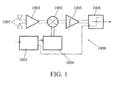
- FIG. 1 illustrates an impulse radio receiver 1000 in accordance with an embodiment of the invention, based on a conventional structure, but incorporating a template generator 1004 in accordance with the invention (a preferred embodiment of the template generator will be described in more detail below).
- the impulse radio receiver comprises an antenna 1007 connected to a signal processing circuitry arranged to process the signals received by the antenna.
- Said signal processing circuitry comprises, in accordance with this embodiment of the invention, a low noise amplifier 1001 connected to the antenna and arranged to amplify the signal received by the antenna, and a so-called analog demodulator or "correlator" comprising the template generator 1004, a mixer 1002 (a passive mixer can be used to reduce power consumption) and an integrator 1005.
- the mixer 1002 is arranged to mix or multiply the signal received from the low noise amplifier 1001 with a pulse train generated by the template generator 1004, and the resulting signal is then integrated by the integrator 1005.
- the signal obtained by the integrator is then submitted to a comparator 1006 which determines the information content of the signal and produces an output signal indicative of said information content.
- the template generator 1004 and the comparator 1006 are synchronised by a timing controller 1003 that provides a synchronisation signal to the template generator 1004 and to the comparator 1006.
- the timing controller 1003 (which can comprise a delay locked loop and an edge selector) is controlled by an external reference clock signal.
- the signal path is differential from the antenna to the integrator, which is advantageous for suppressing noise components in the received signal.
- the above general structure, as shown in figure 1, is conventional and there is thus no need to describe it with more detail here.
- the invention relates to the pulse generator that here constitutes the template generator 1004.
- the rest of the structure is a conventional IR receiver structure. In this case, a single receiver path is used.
- the template generator can also be directly applicable to other structures, for example, to a receiver involving guadrature multiplication (that is, two receiver paths with 90° phase shifted templates), which are useful to reduce the impact of timing errors on the signal-to-noise ratio.
- the template generator can be directly applicable also to a transmitter (such as a UWB-IR transmitter), when adapted to provide the corresponding modulation.
- pulses such as the n:th derivative of the Gaussian pulse
- generating such pulses requires complex generator circuitry.
- the most important requirement for the pulse generator is not the pulse shape itself, but rather its spectral characteristics, which should respect the regulatory emission templates. Now, this can also be achieved with a more simple pulse generator whereby spectral shaping can subsequently be obtained by means of the antenna or by some additional transmission filter.
- the template generator of the present invention can also be used as the pulse generator of an IR-UWB transmitter.
- Control signals can be applied to modify some of the properties of the generated waveform, in accordance with a binary data sequence, so as to implement pulse modulation.
- PPM pulse phase modulation
- PAM pulse amplitude modulation
- OOK on-off keying modulation
- OOK on-off keying modulation
- FIG. 2 illustrates the general constitution of a pulse generator in accordance with a preferred embodiment of the invention.
- the pulse generator is fully differential (the complementary signals, that is, generally, the inverted ones, are conventionally indicated in the drawings by a line above the symbol identifying the respective signal).
- An input signal IN (originated by the timing controller 1003 of figure 1) is supplied to a Voltage Controlled Delay Line (VCDL) 100, comprising a plurality of cascaded delay cells 101 arranged to produce, at their outputs, a plurality of successively delayed versions of the input signal.
- the input signal (IN) is, basically, to be generated by the timing controller every frame, when a pulse is expected to be received.
- the delay line could conveniently comprise 10 delay cells 101, as will be understood from the description following further below.
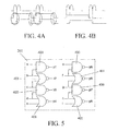
- the structure of a delay cell 101 is schematically illustrated in figure 3. Actually, the same basic type of delay circuit can also be used in the delay locked loop of the timing controller 1003. Now, the stage delay required in the pulse generator can be much smaller than the stage delay required in the timing controller 1003. For this reason, as shown in figure 3, four delay circuits 101a in parallel are used for each branch, to increase its drivability. Two cross coupled weak inverters 101b are placed between the outputs of the delay cell to guarantee the differential operation.
- the basic delay circuit 101a is a CMOS inverter with active loads in both of the pull-up and the pull-down connections.
- the pull-down network is connected to ground (Vss) and the pull-up network is connected to an adjustable supply voltage (V c ) (Vdd represents the high voltage level).
- V c adjustable supply voltage
- Vdd represents the high voltage level
- this buffer 102 is inserted between each delay cell and the following stage of the pulse generator to which the delay line output signals (D1...D10) are to be supplied.
- the buffers are differential in order to produce the corresponding delay line output signal (D1...D10) both according to its "normal” and its "inverted” value.
- the delay line output signals (D1...D10) at the outputs of the buffers 102 are supplied to the so-called pulse generator blocks (201, 202, 301, 302) to generate the corresponding "first pulses" from the respective particular combination of edges.
- These pulse generator blocks comprise conventional complementary CMOS logic gates -NAND (400) and NOR (401)-, and the "first output pulses" (p1-p8) produced by the the pulse generator blocks are used by a pulse combiner circuitry comprising pulse combiner blocks (211, 212, 311, 312) to alternatingly connect an output (OUT: 502, 503, where 503 can be considered to correspond to the differentially complementary output to 502, although it rather corresponds to a delayed version thereof) of the circuit to high voltage (Vdd) or to ground (Vss), as will be described with more detail below.
- Figure 2 schematically illustrates how the pulse generator blocks and the pulse combiner blocks are arranged in two different sections, namely, pulse generator blocks 201 and 202 as well as pulse combiner blocks 211 and 212 are arranged in a "rising edge section" 200, that is, they are arranged to be triggered by the delay line output signals corresponding to a rising edge of the input signal (IN), while pulse generator blocks 301 and 302 and pulse combiner blocks 311 and 312 are arranged in a "falling edge section" 300, that is, they are arranged to be triggered by the delay line output signals corresponding to a falling edge of the input signal (IN).
- pulse generator blocks 301 and 302 and pulse combiner blocks 311 and 312 are arranged in a "falling edge section” 300, that is, they are arranged to be triggered by the delay line output signals corresponding to a falling edge of the input signal (IN).
- the pulse generator blocks and the pulse combiner blocks are grouped in two sections, operated by the rising and falling edges of the input signals coming from the VCDL, respectively.
- power consumption can be reduced, as the pulse generator produces its output pulses in response to both rising and falling edges of the input signal.
- the output pulses are generated only for one of the edges (rising or falling) of the triggering input signal, whereas the opposite edge produces power consumption (in the delay cells, in the logic circuits, etc.) not used for the pulse generation.
- some power is required to reset the initial state of the template/pulse generator, thereby involving a corresponding power consumption.
- the present invention implies that pulses (such as an UWB-IR receiver template) are produced for both edges (that is the rising and the falling one) of the input signal. As a consequence, all the power dissipated is used to generate the output pulses.
- pulses such as an UWB-IR receiver template
- figure 4A shows how (in accordance with prior art) each pulse is generated by one rising edge of an input signal, whereby, in order to produce the four output pulses shown in figure 4A, a total of four rising edges are used, followed by the corresponding falling edges.
- figure 4B which illustrates the principles of the invention, four output pulses are produced by two rising edges and by two falling edges, due to the fact that also the falling edges are used for pulse generation, and not "wasted" as in figure 4A.
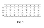
- FIG. 5 schematically illustrates a possible configuration of the pulse generator block 201 (the other pulse generator blocks 202, 301, 302 are identical; the only difference between the pulse generator blocks resides in the way the inputs (a...i) of the logic gates (400, 401) are connected to the outputs (D1...D10, including the "inverse" outputs) of the delay line 100).
- the NAND gates 400 of the pulse generator block generate a negative pulse from a combination of a rising edge followed by a falling edge.
- the NOR gates 401 generate a positive pulse from a falling edge followed by a rising edge.
- the outputs of the logic gates are referred to as p1-p8 in the drawings.
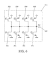
- the pulse combiner blocks can each be constituted as the pulse combiner block 211 illustrated in figure 6, that is, by NMOS 501 and PMOS 500 transistor pairs, the transistors being connected in cascade between supply voltage and ground, the transistor pairs being arranged in parallel and connected, between the two transistors of each transistor pair, to the corresponding output (in this case, 502).
- Figure 65 also schematically illustrate how the outputs (p1-p8) of the logic gates of the pulse generator block are connected to the transistors.
- Each of the two sections (the rising edge section 200, and the falling edge section 300, as explained above) generates two single ended complementary outputs (502, 503), which once considered together form a differential signal required to drive a fully differential passive mixer.
- the corresponding outputs of the two sections (200, 300) can be connected together if the outputs of the pulse combiner blocks (211, 212, 311, 312) are floating in the default state: when one of the pulse combiner blocks (for example, pulse combiner block 211 corresponding to the rising edge section 200) is driving the output 502, the other corresponding pulse combiner block 311 (that is, the corresponding pulse combiner block one in the falling edge section 300) is in the default state.
- the entire pulse generator can be implemented in a 0.18 ⁇ m CMOS process (suitable for implementing high speed devices, such as impulse radio circuits).
- Figures 8A-8F show transistor level simulation results when the circuit is operating at a pulse repetition frequency (PRF) of 200 MHz.
- Figures 8A, 8C and 8E show the waveforms generated from a rising edge of the input signal and figures 8B, 8D and 8F illustrate the corresponding waveforms triggered by a falling edge of the input signal.
- PRF pulse repetition frequency
- figures 8A-8D correspond to the amplitude of the signal in volts (V), and figures 8E and 8F show the amplitudes in mV.
- the horizontal axes all show the time, in nanoseconds.
- Figures 8C and 8D illustrate the corresponding output signals p1-p8 of the pulse generator blocks 201 (figure 8C) and 301 (figure 8D), respectively.
- Figures 8E and 8F illustrate the corresponding "combined" pulse signal obtained at the output 502 of the pulse combiner blocks 211 (figure 8E) and 311 (figure 8F), respectively.
- Figure 9A shows the two single ended outputs of the template, and figure 9B show the differential output waveform (obtained after subtracting the two previous waveforms; this subtraction can be obtained by applying the signals at outputs 502 and 503 of the circuit illustrated in figure 2 to a simple, conventional differential transistor pair, in a conventional manner).
- the vertical axis indicates the amplitude in mV, and in figure 9B, in V; the horizontal axes indicate the time in nanoseconds.
- Figure 9C illustrates a corresponding template spectrum (based on the differential output of figure 9B), centred at 8 GHz (the vertical axis corresponds to the relative amplitude, in dBV, whereas the horizontal axis corresponds to the frequency, in GHz).
- Figure 9B shows both the unloaded (901) and the loaded (902) amplitudes. It can be observed how the template has an unloaded peak-to-peak amplitude of 550 mV, which is reduced to 230 mV when loaded by the local oscillator port of a typical passive mixer.
- the average power consumption of a complete template generator as described above and operating at a supply voltage of 1.8 V has been found to be around 2.0 mW for a pulse repetition frequency of 200 MHz. Most of the power is dissipated by the voltage delay line (approximately 1.55 mW).
Landscapes
- Engineering & Computer Science (AREA)
- Computer Networks & Wireless Communication (AREA)
- Signal Processing (AREA)
- Pulse Circuits (AREA)
Priority Applications (2)
| Application Number | Priority Date | Filing Date | Title |
|---|---|---|---|
| JP2007048613A JP2007243945A (ja) | 2006-03-06 | 2007-02-28 | インパルス無線システムのテンプレート発生等用のパルス発生器およびパルス発生方法 |
| US11/681,862 US7746144B2 (en) | 2006-03-06 | 2007-03-05 | Pulse generator and method of generating pulses, such as for template generation in impulse radio systems |
Applications Claiming Priority (1)
| Application Number | Priority Date | Filing Date | Title |
|---|---|---|---|
| US78001906P | 2006-03-06 | 2006-03-06 |
Publications (1)
| Publication Number | Publication Date |
|---|---|
| EP1833173A1 true EP1833173A1 (fr) | 2007-09-12 |
Family
ID=37432416
Family Applications (1)
| Application Number | Title | Priority Date | Filing Date |
|---|---|---|---|
| EP20060115540 Withdrawn EP1833173A1 (fr) | 2006-03-06 | 2006-06-15 | Générateur d'impulsions et procédé de génération d'impulsions, notamment pour la génération des signaux de référence dans systèmes radio par impulsions |
Country Status (3)
| Country | Link |
|---|---|
| US (1) | US7746144B2 (fr) |
| EP (1) | EP1833173A1 (fr) |
| JP (1) | JP2007243945A (fr) |
Families Citing this family (7)
| Publication number | Priority date | Publication date | Assignee | Title |
|---|---|---|---|---|
| KR100839592B1 (ko) * | 2006-10-16 | 2008-06-20 | 한국전자통신연구원 | 디지털 방식을 이용한 초광대역 펄스 생성기 및 그 방법 |
| US20080118016A1 (en) * | 2006-11-20 | 2008-05-22 | Yu-Min Chuang | Synchronous circuit of receiving device of wireless transmission system |
| GB201015729D0 (en) * | 2010-09-20 | 2010-10-27 | Novelda As | Pulse generator |
| GB201015730D0 (en) | 2010-09-20 | 2010-10-27 | Novelda As | Continuous time cross-correlator |
| KR101744202B1 (ko) * | 2010-12-03 | 2017-06-09 | 울산과학기술원 | 펄스 생성기 및 펄스 생성 방법 |
| US9958540B2 (en) * | 2015-02-24 | 2018-05-01 | S-1 Corporation | Ultra-wideband transceiver, signal transmission and reception method thereof, and ultra-wideband radar sensor including the same |
| US11209521B2 (en) * | 2019-06-05 | 2021-12-28 | The Boeing Company | Methods and systems for establishing prototype pulses |
Citations (2)
| Publication number | Priority date | Publication date | Assignee | Title |
|---|---|---|---|---|
| EP1499046A2 (fr) * | 1998-09-03 | 2005-01-19 | Time Domain Corporation | Système et procédé pour la génération de temporisation précise |
| US20060062278A1 (en) * | 2004-09-06 | 2006-03-23 | Satoru Ishii | Ultrawideband radio transmitter, ultrawideband radio receiver, and ultrawideband radio transmission/reception system |
Family Cites Families (6)
| Publication number | Priority date | Publication date | Assignee | Title |
|---|---|---|---|---|
| FR2658015B1 (fr) * | 1990-02-06 | 1994-07-29 | Bull Sa | Circuit verrouille en phase et multiplieur de frequence en resultant. |
| JP2861465B2 (ja) * | 1991-05-16 | 1999-02-24 | 日本電気株式会社 | 周波数逓倍回路 |
| US6037812A (en) * | 1998-05-18 | 2000-03-14 | National Semiconductor Corporation | Delay locked loop (DLL) based clock synthesis |
| US6980613B2 (en) | 2003-09-30 | 2005-12-27 | Pulse-Link, Inc. | Ultra-wideband correlating receiver |
| US20070190953A1 (en) | 2004-01-06 | 2007-08-16 | Adrian Tan Eng Choon | Method of generating uwb pulses |
| JP2007228546A (ja) * | 2005-09-13 | 2007-09-06 | Seiko Epson Corp | パルス発生回路およびこの回路を用いた電子装置、携帯電話機、パーソナルコンピュータ、ならびに、この回路を用いる情報伝送方法 |
-
2006
- 2006-06-15 EP EP20060115540 patent/EP1833173A1/fr not_active Withdrawn
-
2007
- 2007-02-28 JP JP2007048613A patent/JP2007243945A/ja not_active Withdrawn
- 2007-03-05 US US11/681,862 patent/US7746144B2/en not_active Expired - Fee Related
Patent Citations (2)
| Publication number | Priority date | Publication date | Assignee | Title |
|---|---|---|---|---|
| EP1499046A2 (fr) * | 1998-09-03 | 2005-01-19 | Time Domain Corporation | Système et procédé pour la génération de temporisation précise |
| US20060062278A1 (en) * | 2004-09-06 | 2006-03-23 | Satoru Ishii | Ultrawideband radio transmitter, ultrawideband radio receiver, and ultrawideband radio transmission/reception system |
Also Published As
| Publication number | Publication date |
|---|---|
| US20070210848A1 (en) | 2007-09-13 |
| JP2007243945A (ja) | 2007-09-20 |
| US7746144B2 (en) | 2010-06-29 |
Similar Documents
| Publication | Publication Date | Title |
|---|---|---|
| US7746144B2 (en) | Pulse generator and method of generating pulses, such as for template generation in impulse radio systems | |
| US6937667B1 (en) | Apparatus, system and method for flip modulation in an impulse radio communications system | |
| US6735238B1 (en) | Ultra wideband communication system, method, and device with low noise pulse formation | |
| US7221724B2 (en) | Precision timing generation | |
| EP1987589B1 (fr) | Dispositifs comportant une ligne de retard pour l'application d'une temporisation variable à un signal d'horloge | |
| WO2006054405A1 (fr) | Dispositif de transmission, dispositif de reception et systeme de communication | |
| US8724677B1 (en) | Architecture for ultra-wideband radio | |
| US7394866B2 (en) | Ultra wideband communication system, method, and device with low noise pulse formation | |
| KR100818173B1 (ko) | 고속 디지털 샘플러 및 이를 이용한 근거리 임펄스 비동기무선 통신 시스템 | |
| US8437377B2 (en) | Pulse generator, transmitter-receiver, and pulse generation method | |
| US7804347B2 (en) | Pulse generator circuit and communication apparatus | |
| Stoica et al. | An ultra wideband low complexity circuit transceiver architecture for sensor networks | |
| US7855589B2 (en) | Pulse generator circuit and communication apparatus | |
| JP4408091B2 (ja) | 無線送信方法および無線送信機 | |
| US7075382B2 (en) | Method and apparatus for modulating a pulse signal with a bit stream | |
| US8817894B2 (en) | Method and device for sending signals between a radio frequency circuit and a baseband circuit | |
| JP4408092B2 (ja) | 無線通信方法、無線送信方法、無線通信システムおよび無線送信機 | |
| JP5626044B2 (ja) | インパルス無線伝送装置、およびインパルス無線伝送装置の送信方法 | |
| Yuan et al. | A fully integrated CMOS transmitter for ultra-wideband applications | |
| Thotahewa et al. | Analysis of pulse based UWB transmission techniques for wireless sensors | |
| Yoshizumi et al. | All digital transmitter scheme and transceiver design for pulse-based ultra-wideband radio | |
| Raju et al. | DSSS IR UWB transceiver for intra/inter chip wireless interconnect in future ULSI using reconfigurable monocycle pulse | |
| JP2005277642A (ja) | Uwb通信装置 | |
| US20060023874A1 (en) | Method and multiline scrambled clock architecture with random state selection for implementing lower electromagnetic emissions | |
| Salahuddin et al. | Reconfigurable Monocycle Pulse Generation for Impulse Radio Based UWB Transceiver |
Legal Events
| Date | Code | Title | Description |
|---|---|---|---|
| PUAI | Public reference made under article 153(3) epc to a published international application that has entered the european phase |
Free format text: ORIGINAL CODE: 0009012 |
|
| AK | Designated contracting states |
Kind code of ref document: A1 Designated state(s): AT BE BG CH CY CZ DE DK EE ES FI FR GB GR HU IE IS IT LI LT LU LV MC NL PL PT RO SE SI SK TR |
|
| AX | Request for extension of the european patent |
Extension state: AL BA HR MK YU |
|
| 17P | Request for examination filed |
Effective date: 20070919 |
|
| AKX | Designation fees paid |
Designated state(s): AT BE BG CH CY CZ DE DK EE ES FI FR GB GR HU IE IS IT LI LT LU LV MC NL PL PT RO SE SI SK TR |
|
| GRAP | Despatch of communication of intention to grant a patent |
Free format text: ORIGINAL CODE: EPIDOSNIGR1 |
|
| RIN1 | Information on inventor provided before grant (corrected) |
Inventor name: IKEDA, MASAYUKI Inventor name: CAIRO MOLINS, JOSEP IGN.EPSON EUROPE ELECTRONICS Inventor name: BARAJAS OJEDA, ENRIQUETECH. UNIV. CATALONIA Inventor name: MATEO PENA, DIEGO Inventor name: GONZALEZ JIMENEZ, JOSE LUIS |
|
| STAA | Information on the status of an ep patent application or granted ep patent |
Free format text: STATUS: THE APPLICATION IS DEEMED TO BE WITHDRAWN |
|
| 18D | Application deemed to be withdrawn |
Effective date: 20090303 |