EP1825282B1 - Signalmodul mit verminderter rückstrahlung - Google Patents
Signalmodul mit verminderter rückstrahlung Download PDFInfo
- Publication number
- EP1825282B1 EP1825282B1 EP05853612A EP05853612A EP1825282B1 EP 1825282 B1 EP1825282 B1 EP 1825282B1 EP 05853612 A EP05853612 A EP 05853612A EP 05853612 A EP05853612 A EP 05853612A EP 1825282 B1 EP1825282 B1 EP 1825282B1
- Authority
- EP
- European Patent Office
- Prior art keywords
- conductors
- signal module
- signal
- conductor
- electromagnetic
- Prior art date
- Legal status (The legal status is an assumption and is not a legal conclusion. Google has not performed a legal analysis and makes no representation as to the accuracy of the status listed.)
- Not-in-force
Links
- 239000004020 conductor Substances 0.000 claims abstract description 119
- 238000000034 method Methods 0.000 claims abstract description 19
- 230000005540 biological transmission Effects 0.000 claims description 50
- 239000003989 dielectric material Substances 0.000 claims description 30
- 239000007787 solid Substances 0.000 claims 32
- 229910001369 Brass Inorganic materials 0.000 claims 2
- 239000010951 brass Substances 0.000 claims 2
- OKTJSMMVPCPJKN-UHFFFAOYSA-N Carbon Chemical compound [C] OKTJSMMVPCPJKN-UHFFFAOYSA-N 0.000 claims 1
- RYGMFSIKBFXOCR-UHFFFAOYSA-N Copper Chemical compound [Cu] RYGMFSIKBFXOCR-UHFFFAOYSA-N 0.000 claims 1
- BQCADISMDOOEFD-UHFFFAOYSA-N Silver Chemical compound [Ag] BQCADISMDOOEFD-UHFFFAOYSA-N 0.000 claims 1
- 229910045601 alloy Inorganic materials 0.000 claims 1
- 239000000956 alloy Substances 0.000 claims 1
- XAGFODPZIPBFFR-UHFFFAOYSA-N aluminium Chemical compound [Al] XAGFODPZIPBFFR-UHFFFAOYSA-N 0.000 claims 1
- 229910052782 aluminium Inorganic materials 0.000 claims 1
- 229910052802 copper Inorganic materials 0.000 claims 1
- 239000010949 copper Substances 0.000 claims 1
- PCHJSUWPFVWCPO-UHFFFAOYSA-N gold Chemical compound [Au] PCHJSUWPFVWCPO-UHFFFAOYSA-N 0.000 claims 1
- 229910052737 gold Inorganic materials 0.000 claims 1
- 239000010931 gold Substances 0.000 claims 1
- 229910002804 graphite Inorganic materials 0.000 claims 1
- 239000010439 graphite Substances 0.000 claims 1
- 229910052709 silver Inorganic materials 0.000 claims 1
- 239000004332 silver Substances 0.000 claims 1
- 230000005672 electromagnetic field Effects 0.000 abstract description 7
- 238000012360 testing method Methods 0.000 description 22
- 239000000523 sample Substances 0.000 description 19
- 230000001902 propagating effect Effects 0.000 description 8
- 238000013459 approach Methods 0.000 description 6
- 230000005684 electric field Effects 0.000 description 6
- 239000000463 material Substances 0.000 description 6
- 239000013598 vector Substances 0.000 description 6
- 239000003570 air Substances 0.000 description 5
- 238000010998 test method Methods 0.000 description 5
- 230000001419 dependent effect Effects 0.000 description 4
- 238000004088 simulation Methods 0.000 description 4
- 230000008878 coupling Effects 0.000 description 3
- 238000010168 coupling process Methods 0.000 description 3
- 238000005859 coupling reaction Methods 0.000 description 3
- 230000000694 effects Effects 0.000 description 3
- 238000004519 manufacturing process Methods 0.000 description 3
- 125000006850 spacer group Chemical group 0.000 description 3
- 230000003247 decreasing effect Effects 0.000 description 2
- -1 polytetrafluoroethylene Polymers 0.000 description 2
- 239000004698 Polyethylene Substances 0.000 description 1
- 229920004738 ULTEM® Polymers 0.000 description 1
- 230000000712 assembly Effects 0.000 description 1
- 238000000429 assembly Methods 0.000 description 1
- 239000011324 bead Substances 0.000 description 1
- 230000002457 bidirectional effect Effects 0.000 description 1
- 238000004364 calculation method Methods 0.000 description 1
- 238000012512 characterization method Methods 0.000 description 1
- 238000005094 computer simulation Methods 0.000 description 1
- 230000007423 decrease Effects 0.000 description 1
- 230000001627 detrimental effect Effects 0.000 description 1
- 230000006872 improvement Effects 0.000 description 1
- 238000003780 insertion Methods 0.000 description 1
- 230000037431 insertion Effects 0.000 description 1
- 238000003754 machining Methods 0.000 description 1
- 230000007246 mechanism Effects 0.000 description 1
- 238000012986 modification Methods 0.000 description 1
- 230000004048 modification Effects 0.000 description 1
- 230000003287 optical effect Effects 0.000 description 1
- 230000010287 polarization Effects 0.000 description 1
- 229920000573 polyethylene Polymers 0.000 description 1
- 229920001343 polytetrafluoroethylene Polymers 0.000 description 1
- 239000004810 polytetrafluoroethylene Substances 0.000 description 1
- 229920000915 polyvinyl chloride Polymers 0.000 description 1
- 239000004800 polyvinyl chloride Substances 0.000 description 1
- 230000008569 process Effects 0.000 description 1
- 230000008054 signal transmission Effects 0.000 description 1
- 230000011664 signaling Effects 0.000 description 1
- 238000012546 transfer Methods 0.000 description 1
Images


Classifications
-
- G—PHYSICS
- G01—MEASURING; TESTING
- G01R—MEASURING ELECTRIC VARIABLES; MEASURING MAGNETIC VARIABLES
- G01R31/00—Arrangements for testing electric properties; Arrangements for locating electric faults; Arrangements for electrical testing characterised by what is being tested not provided for elsewhere
- G01R31/26—Testing of individual semiconductor devices
-
- G—PHYSICS
- G01—MEASURING; TESTING
- G01R—MEASURING ELECTRIC VARIABLES; MEASURING MAGNETIC VARIABLES
- G01R31/00—Arrangements for testing electric properties; Arrangements for locating electric faults; Arrangements for electrical testing characterised by what is being tested not provided for elsewhere
- G01R31/28—Testing of electronic circuits, e.g. by signal tracer
- G01R31/2851—Testing of integrated circuits [IC]
- G01R31/2886—Features relating to contacting the IC under test, e.g. probe heads; chucks
- G01R31/2889—Interfaces, e.g. between probe and tester
-
- G—PHYSICS
- G01—MEASURING; TESTING
- G01R—MEASURING ELECTRIC VARIABLES; MEASURING MAGNETIC VARIABLES
- G01R31/00—Arrangements for testing electric properties; Arrangements for locating electric faults; Arrangements for electrical testing characterised by what is being tested not provided for elsewhere
- G01R31/28—Testing of electronic circuits, e.g. by signal tracer
- G01R31/317—Testing of digital circuits
- G01R31/3181—Functional testing
- G01R31/3183—Generation of test inputs, e.g. test vectors, patterns or sequences
-
- H—ELECTRICITY
- H01—ELECTRIC ELEMENTS
- H01L—SEMICONDUCTOR DEVICES NOT COVERED BY CLASS H10
- H01L22/00—Testing or measuring during manufacture or treatment; Reliability measurements, i.e. testing of parts without further processing to modify the parts as such; Structural arrangements therefor
-
- G—PHYSICS
- G01—MEASURING; TESTING
- G01R—MEASURING ELECTRIC VARIABLES; MEASURING MAGNETIC VARIABLES
- G01R1/00—Details of instruments or arrangements of the types included in groups G01R5/00 - G01R13/00 and G01R31/00
- G01R1/02—General constructional details
- G01R1/06—Measuring leads; Measuring probes
-
- G—PHYSICS
- G01—MEASURING; TESTING
- G01R—MEASURING ELECTRIC VARIABLES; MEASURING MAGNETIC VARIABLES
- G01R31/00—Arrangements for testing electric properties; Arrangements for locating electric faults; Arrangements for electrical testing characterised by what is being tested not provided for elsewhere
- G01R31/28—Testing of electronic circuits, e.g. by signal tracer
- G01R31/282—Testing of electronic circuits specially adapted for particular applications not provided for elsewhere
- G01R31/2822—Testing of electronic circuits specially adapted for particular applications not provided for elsewhere of microwave or radiofrequency circuits
Definitions
- the present invention relates to electronic interfacing and more particularly, an apparatus and method for substantially reducing electromagnetic reflections in a signal interface module.
- IC testing systems typically include a test head and a probe card.
- Packaged part testing systems typically include a test head and a device under test (DUT) board.
- the probe card or DUT board includes a pattern of contacts for electrically probing or connecting to portions of an integrated circuit.
- the test head is configured to drive various contacts of the probe card or DUT board to carry out particular test procedures within the IC.
- the test head receives output signals from the IC via the contacts of the probe card or DUT board.
- the output signals are indicative of electrical characteristics of the IC under test.
- the probe card or DUT board and the test head are uniquely configured for a particular IC and, in some cases, a particular test procedure. Accordingly, the probe card or DUT board and/or the test head must be changed for different ICs and test procedures.
- the test head is electrically coupled to the probe card or DUT board with an interface apparatus.
- the interface apparatus may be, for example, a zero insertion force socket or a "pogo" unit.
- a pogo unit engages the test head, or some intermediate coupling structure associated with the test head, and the probe card or DUT board.
- the pogo unit includes an array of spring-loaded contact pins referred to as Pogo Pins®.
- the spring pins act as signal and ground conductors, and are arranged to electrically couple contacts on the probe card or DUT board to corresponding contacts on the test head.
- the spring force of the spring pins helps to maintain uniformity of electrical contact between the various contacts of the probe card or DUT board and the test head.
- the spring pins When the test head and probe card or DUT board are engaged with the pogo unit exerting pressure against the spring pins, the spring pins respond with a spring force that enhances coupling pressure.
- the resilience of the pins generally ensures adequate coupling pressure despite planar deformation of the test head or the probe card or DUT board during a test procedure.
- the conductors are required to carry signals having very high frequency components, from 100's of MHz to 10 GHz In the near future and to 10's of GHz in the more distant future.
- the transmission line characteristic impedance of the signal path between the probe card or DUT board and the test head is of prime interest.
- the characteristic impedance of all elements in the signal path should be closely matched.
- ATE interface signal modules typically employ dielectric materials to structurally support electrical transmission lines. These dielectric materials provide an electrically insulating boundary between adjacent transmission line elements, but also cause discontinuities in the characteristic impedance along the path of the transmission line. Discontinuities in characteristic impedance along a transmission line can cause undesirable effects that include increased reflection coefficients levels, consequent decreased transmission coefficient levels, both of which are frequency dependent, that causes unleveled channel performance detrimental to the signal integrity of the signal module and its ability to perform ATE signal characterization. In many applications it is thus desirable to remove the reflections of electromagnetic fields as they propagate through the impedance discontinuities caused by the differing dielectric constants.
- WO 02/07265 A describes a contact apparatus particular useful with test equipment.
- a double-ended, coaxial contact assembly has a center probe rod mounted in the bore of a dielectric center spacer bushing and mounts a probe contact assembly on each end of the center probe rod.
- the center probe rod is received in a ground sleeve with the probe contact assemblies maintained in coaxial relationship with the ground sleeve by a dielectric outer spacer bushing.
- a movable ground plunger is slidably received in each end of the ground sleeves and biased outwardly by respective ground plunger coil springs.
- the center spacer bushing is provided with an axially extending sleeve disposed between the respective probe contact assembly and the ground sleeve.
- the invention is defined by the subject-matter of the independent claims.
- the dependent claims are directed to advantageous embodiments.
- the signal module for electrically interfacing with an electronic device.
- the signal module includes a dielectric and a conductor extending through a surface of the dielectric.
- the surface of the dielectric is located away from perpendicular relative to an axis of the conductor and is located based on an electromagnetic field produced as a result of a signal flowing through the conductor.
- the method includes the step of providing a signal module.
- the signal module includes a dielectric and a conductor extending through a surface of the dielectric.
- the surface of the dielectric is away from perpendicular relative to an axis of the conductor and the surface is based on an electromagnetic field produced as a result of a signal flowing through the conductor.
- the method further includes the steps of providing the electromagnetic signal to one end of the conductor in the signal module and transmitting the signal through the conductor.
- the signal connector includes a dielectric having a countersink provided on each of a first surface and a second surface opposite the first surface.
- the signal connector also includes a conductor that extends through the countersink of the first surface of the dielectric and the countersink of the second surface of the dielectric.
- the dielectric provides mechanical support to the conductor.
- the countersinks are provided at a bevel angle relative to an axis of the conductor and located based on an electromagnetic field produced as a result of a signal flowing through the conductor.
- the signal module includes a plurality of spring pins and a first and second retainer cap.
- Each retainer cap is of dielectric materials.
- Each retainer cap includes a top portion having a plurality of countersinks provided in each of a first surface and a second surface opposite the first surface and a plurality of bores extending between the plurality of countersinks provided in the first surface and the second surface.
- Each retainer cap also includes a side portion that is coupled to the top portion. The side portion encloses the plurality of spring pins.
- the plurality of spring pins are disposed in the plurality of bores, respectively.
- the countersinks are provided at a bevel angle relative to an axis of the conductor and located based on an electromagnetic field produced as a result of a plurality of signals flowing through the plurality of spring pins, respectively.
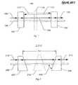
- Figure 1 describes a conventional ATE interface signal module 100.
- An ATE interface electromagnetic signal 106 is transmitted through signal module 100 along spring pin 104.
- the electromagnetic signal propagates in the region 108 surrounding the surfaces of the spring pins, (multiple spring pins not shown) and encounters dielectric caps 102 at the module ends along with any dielectric shims 116 within the signal module.
- reflections 112 of the electromagnetic signal occur when the electromagnetic signal encounters the boundary interface between the media surrounding spring pin 104 and the dielectric caps 102.
- a typical ATE interface signal module may employ dielectric caps whose dielectric constant is greater than air. This creates a characteristic impedance mismatch, resulting in the electromagnetic reflections 112.
- the magnitude of the electromagnetic reflections increase as the dielectric constant of the dielectric caps increase. Additionally, the forward transmission coefficient suffers loss causing decreased transmission through the signal module.
- the final electromagnetic signal 110 transmitted through the conventional signal module may include transmission loss and crosstalk from adjacent spring pins.
- Efforts to reduce electromagnetic reflections in an ATE interface signal module have attempted to compensate for the capacitive effect of the dielectric cap. For example, the spring pin diameter in a portion of the dielectric cap has been adjusted in an effort to achieve an impedance match.
- the present invention produces an electromagnetic impedance match by implementing the condition where the plane of the incident TM (transverse magnetic) field of the electromagnetic wave propagating along the axis of the signal module is parallel with the surface of the dielectric boundary.
- An angle of the dielectric boundary surface is thus determined based on the electromagnetic field produced as a result of the signal flowing through the signal module.
- this is desirably accomplished by creating a bevel angle at the boundary of the media between the spring pins and the dielectric caps.
- An exemplary embodiment of the present invention comprises a signal module including a conductor and a low loss dielectric.
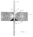
- dielectrics 202 and 204 and conductor 208 are shown in Figure 2 .
- Figure 2 illustrates a signal module 200 according to an exemplary embodiment of the present invention.
- the conductor may pass through dielectrics 202 and 204 in signal module 200. Additional dielectrics such as dielectric 216 may also be positioned along the length of conductor to provide further support to the conductor.
- An electromagnetic signal 210 may be sent into one end of the exemplary signal module.
- the electromagnetic signal is an electromagnetic wave that propagates along the axis of conductor 208.
- the electromagnetic signal desirably passes through dielectrics 202 and 204 without producing reflections in region 212 between dielectrics 202 and 204.
- Signal 214 that is transmitted out of signal module 200 desirably has no transmission loss from passing through dielectrics 202 and 204.
- ATE interface signals typically have a bandwidth in the GHz region.
- Signal module 200 desirably operates in the frequency region between DC and at least 30 GHz and higher.
- Exemplary signal module 200 may operate at a substantially higher bandwidth or within a more limited bandwidth.
- the exemplary signal module is not limited to ATE interface signals and may be used for other applications, such as connectors that include internal dielectric inserts intended to mechanically support electrical conductors within the connector but also obstruct the propagation of electromagnetic signals that pass through them.
- Signal module 200 shown here presents dielectric 204 as having one angle 206. This is being shown for illustrative purposes only.
- dielectrics 202 and 204 are at the same bevel angle 206.
- dielectrics 202 and 204 show only one surface with bevel angle 206, in the exemplary embodiment, all surfaces are desirably at a specific bevel angle. Additionally, dielectrics 202 and 204 only show one segment of the specific bevel angle.
- the bevel angle is a conical shaped countersink 302 of Figure 3 , which is convenient for fabrication.
- a dielectric 204 has a first surface 204a and a second surface 204b.
- a conductor 208 passes through first surface 204a having a countersink 302.
- Countersink 302 is desirably at angle 206 relative to a central axis along the length of conductor 208.
- Conductor 208 further passes through second surface 204b, also having a countersink 302. It is desirable that surfaces 204a and 204b each have countersinks 302, both at bevel angle 206.
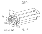
- Exemplary conductor 208 may be included in a pseudo-coaxial transmission line comprised of a plurality of conductors. Pseudo-coaxial transmission lines are commonly known by one skilled in the art.
- Figure 4 illustrates a known in the art pseudo-coaxial transmission line 400 composed of five parallel spring pins 402 and 404.
- center pin 404 carries the electromagnetic signal and the other four spring pins 402, which are arranged to surround center pin 404 are electrically grounded.
- This and other potentially useful configurations are shown, for example, in Reference Data for Radio Engineers, 4th Edition. New York: International Telephone & Circuit Corp., 1957 .
- the present invention is not limited to spring pin arrangement 400 or to a pseudo-coaxial transmission line.
- the transmission lines used in exemplary signal module 200 typically seek to achieve a characteristic impedance of 50 Ohms. This characteristic impedance matches the impedance of typical coaxial cables, printed circuit boards microstrip transmission lines or other electrical devices that may be attached to the exemplary signal module. Signal module 200 may be designed to achieve other characteristic impedance values.
- the characteristic impedance of a transmission line may be governed by the geometric arrangement of the spring pins, the diameter of the spring pins, the spacing distance between spring pins, and the dielectric constant of the media between the pins.
- Other media may include other dielectric medium with a low loss tangent and stable, frequency independent dielectric constant.
- Exemplary signal module 200 with conductor 208 may operate with a planar electric field vector from an electromagnetic signal, such as but not limited to TM01 or TE11 wave modes for a circular geometric arrangement of conductors forming a transmission line, or TE10 or TM11 wave modes for a rectangular geometry of conductors forming a transmission line.
- the exemplary signal module also desirably operates with electromagnetic signals having distorted electric field vector.
- a distorted TM field vector may occur where conductor 208 is a pseudo-coaxial transmission line or in other configurations.
- Dielectrics 202 and 204 may include dielectric material having a dielectric constant between 1 to 5 over a frequency range of DC to at least 30 GHz and higher.
- the frequency range for which the dielectric constant is desirably between 1 to 5 may be substantially higher.
- the dielectric constant is desirably constant over a preferred bandwidth.
- the dielectric constant value and frequency range desirably depends upon the application of the exemplary signal module. The desired dielectric constant value and frequency range may vary with the type of input signal without affecting the scope of the present invention.
- the dielectric material also desirably includes the property of a loss tangent less than 0.1 over the frequency range of DC to at least 30 GHz and higher.
- the frequency range for which the loss tangent is desirably less than 0.1 may be substantially higher.
- the loss tangent required depends upon the application of the signal module. ATE interface signals may require lower loss tangents than other applications.
- Common dielectric materials used in exemplary signal module 200 may include polytetrafluoroethylene, FR4, Ultem ® 1000, Rexolite ® , polyethylene, polyvinylchloride and air. Other materials may be used provided they have a low loss tangent (for example less than 0.1) and dielectric constant suitable for the application requirements. All dielectric materials, including those listed here, exhibit some loss, albeit a small loss that may be considered negligible.
- an electromagnetic impedance match at the boundary of two media with differing dielectric constants may be achieved if the plane of the incident TM field of the electromagnetic wave propagating along the axis of the signal module is parallel with the surface of the dielectric boundary, and the boundary is at a specific bevel angle. This bevel angle is determined from the angle where the electromagnetic reflection approaches a zero value.
- the surface of the dielectric of the exemplary embodiment is desirably smooth and contains a straight line parallel to the TM field plane of incidence where they intersect and where the electromagnetic wave propagates along a linear axis.
- the surface of the dielectric desirably conforms to an isosurface of the TM field for other electromagnetic wave conditions.
- the angle where electromagnetic reflections approach a minimum value may be calculated using the principles of a Brewster angle.
- the Brewster angle is common in the art of optical and quasi-optical systems.
- ⁇ B the Brewster angle
- ⁇ 1 and ⁇ 2 are the dielectric constants of regions 1 and 2 respectively
- ⁇ T is the refractive angle of region 2.
- the bevel angle is dependent upon the dielectric constant of the dielectric, the dielectric constant of the media surrounding the conductor, and the angle of the TM field vector from the electromagnetic signal propagating along the conductor.
- the bevel angle is desirably further modified to account for the distortion. Therefore, the bevel angle is not a classic Brewster angle, but an angle that accounts for electric field distortion caused by the type of conductor, such as a pseudo-coaxial transmission line.
- the criteria for an electromagnetic impedance match are those as defined in equation (2) but the implementation desirably requires modification to account for electric field distortion in order to accommodate those criteria.
- the improvement in transmission is broadband and not dependent upon the signal frequency.
- Frequency dependence is limited by the frequency dependence of the dielectric material permittivity.
- frequency dependence is also limited by the electromagnetic mode cut-off frequency well known to transmission line designers.
- the present invention may be extended to a signal module with multiple conductors, as shown in Figure 5.
- Figure 5 shows a cross-sectioned portion of one end of a dielectric cap 500. Multiple conductors 502, 504 and 506 extend through the dielectric cap 500 and out of a signal module according to an exemplary embodiment of the present invention.
- Figure 5 shows bevel angles 508, 510 and 512 corresponding to conductors 502, 504, and 506.
- the bevel angles illustrated here more accurately depict the implementation of bevel angles on the dielectric surface.
- the bevel angles are desirably countersinks on the dielectric.
- the multiple countersinks are desirably adjacent to or intersect each other.
- the conductors illustrated in the embodiment of Figure 5 may each represent an individual conductor of, for example, a five-wire a pseudo-coaxial transmission line such as illustrated in Figure 4 or other transmission lines, or signal carrying connector.
- the exemplary embodiment is not limited to a device of three conductors.
- the exemplary signal module may contain any number of conductors in a planar or other suitable arrangement. The conductors may be spaced apart and in such an arrangement to provide an appropriate characteristic impedance match to its connecting devices.
- the bevel angle applied to the surface of the dielectric for each respective conductor causes the electromagnetic reflection along each conductor to approach a minimum value.
- the even mode is defined as simultaneous signals propagating in a parallel direction, in contrast to an odd mode where simultaneous signals are propagating in an anti-parallel direction.
- the exemplary embodiment may include any combination of even and odd mode propagation conditions simultaneously.
- a first electromagnetic signal may propagate into the end of conductor 502 while a second electromagnetic signal may propagate out of the end of conductor 504.
- the second electromagnetic signal thus propagates in a direction opposite the first electromagnetic signal.
- Respective bevel angles 508, 510 and 512 may each be designed for the specific electromagnetic signal and may be of a different angle to remove reflections for the particular electromagnetic signal. This allows manufacture of a signal module suited to a particular application. The resulting signal module will have a minimum of channel cross-talk and a maximum of respective signal transmission.
- Figures 6 illustrates an exemplary pseudo-coaxial transmission line 600 with five dielectrics 606 spaced apart from each other along pseudo-coaxial transmission line 600.
- Each dielectric 606 has a bevel angle countersink (not shown) on both sides of dielectric 606 determined as described above.
- Pseudo-coaxial transmission line 600 has five spring pins 602 and 604.
- Center spring pin 604 carries the electromagnetic signal and the other four spring pins 602, which are arranged to surround center pin 604 are electrically grounded.
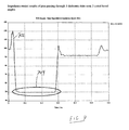
- Impedance model simulation results 702 illustrate the impedance in ohms of an electromagnetic signal propagating through exemplary pseudo-coaxial transmission line 600 versus time in ns.
- the impedance is about 50 ohms, as illustrated by region 704.
- Exemplary embodiment 600 demonstrates that although the electromagnetic signal encounters 10 boundary condition changes (two for each dielectric 606) the bevel angle countersinks on each dielectric significantly reduce an impedance mismatch, thus maintaining the impedance at about 50 ohms.
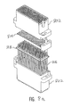
- a retainer cap 802 of dielectric material covers and supports spring pins 816.
- a section of retainer cap 802 is further illustrated in Figure 8b .
- Retainer cap 802 has a top portion 804 and a side portion 812.
- a first surface of top portion 804 includes a plurality of bevel angle countersinks 806.
- a plurality of apertures 808 extends between bevel angle countersinks 806 and a second surface of top portion 804.
- a second surface 810 of top portion 804 is a flat surface and does not have bevel angle countersinks due to machining limitations.
- a bevel angle shim 814 is of dielectric material having a first surface that is flat and a second surface with bevel angle countersinks. Bevel angle shim further includes apertures corresponding to the apertures in the retainer cap 802 and the countersinks of bevel angle shim 814. The first surface of bevel angle shim 814 is disposed adjacent to the second surface 810 of top portion 804 of retainer cap 802. The combination of dielectric retainer cap 802 and bevel angle shim 812 function as one retainer with both surfaces having bevel angle countersinks.
- An assembly shim 818 is disposed between side portion 812 of a first retainer cap 802 and a side portion 812 of a second retainer cap 802.
- Assembly shim 818 has apertures corresponding to the apertures in first retainer cap 802.
- Assembly shim 818 is desirably of dielectric material with bevel angle countersinks machined on both sides corresponding to the apertures.
- Assembly shim 818 may provide support to spring pins 816.
- a second retainer cap 802 and bevel angle shim 814 as described above are coupled together to function as one retainer with both surfaces having bevel angle countersinks.
- Both second retainer cap 802 and second bevel angle shim 814 further include apertures that correspond to the apertures in first retainer cap 802.
- a plurality of spring pins 816 extend and are supported through the apertures between top portion 804 of first retainer cap 802, first bevel angle shim 814, assembly shim 818, a second bevel angle shim 814 and top portion 804 of a second retainer cap 802. Side portions 812 of first and second retainer caps 802 enclose spring pins 816 within exemplary ATE signal interface module 800.
- ATE signal Interface module 800 all dielectric boundaries are thus provided with countersink bevel angles designed as described above according to an exemplary method of the present invention. Exemplary module 800 thus does not suffer from impedance mismatch.
- the invention is defined by the following claims.
Claims (43)
- Signalmodul (200; 800), um mit einer elektronischen Vorrichtung eine elektrische Schnittstelle zu bilden, wobei das Signalmodul (200; 800) umfasst:mehrere Leiter (208; 404; 502, 504, 506; 604), die konfiguriert sind, um jeweilige elektromagnetische Signale (210) zu transportieren; undwenigstens einen festen Träger (202, 204; 500; 802) aus dielektrischem Material, der eine Oberfläche (204a, 204b) senkrecht zu Achsen der Leiter (208; 404; 502, 504, 506; 604) besitzt, wobei der feste Träger (202, 204; 500; 802) Vertiefungen (303; 806) besitzt, die in Bezug auf diese Achsen symmetrisch sind, wobei die Vertiefungen (302; 806) jeweils auf der Oberfläche (204a, 204b) eine Basis und innerhalb des festen Trägers (202, 204; 500; 802) eine Spitze besitzen, wobei die Vertiefung (302; 806) jeweils unter einem Schrägungswinkel (206; 508, 510, 512) in Bezug auf die Achsen vorgesehen ist, wobei der Schrägungswinkel so gewählt ist, dass zwischen den dielektrischen Grenzen im Wesentlichen null Reflexionen vorhanden sind,wobei sich die Leiter (208; 404; 502, 504, 506; 604) durch den festen Träger (202, 204; 500; 802) durch jede Spitze der Vertiefungen (302; 806) erstrecken,
wobei jeder der Leiter (208; 404; 502, 504, 506; 604) von den jeweils anderen der Leiter (208; 404; 502, 504, 506; 604) beabstandet ist. - Signalmodul (200; 800) nach Anspruch 1, wobei der feste Träger (202, 204; 500; 802) einer von mehreren festen Trägern (202, 204; 500; 802) ist, wobei die mehreren festen Träger (202, 204; 500; 802) längs der Achse des Leiters (208; 404; 502, 504, 506; 604) voneinander beabstandet sind.
- Signalmodul (200; 800) nach Anspruch 1, wobei das dielektrische Material eine Verlustziffer von weniger als 0,1 in einem Frequenzbereich von Gleichstrom bis 30 GHz aufweist.
- Signalmodul (200; 800) nach Anspruch 1, wobei das dielektrische Material eine Dielektrizitätskonstante im Bereich von 1 bis 5 hat, die über einen Frequenzbereich von Gleichstrom bis 30 GHz konstant bleibt.
- Signalmodul (200; 800) nach Anspruch 1, wobei der Leiter (208; 404; 502, 504, 506; 604) aus Kupfer und/oder Messing und/oder Messinglegierungen und/oder Aluminium und/oder Silber und/oder Graphit und/oder Gold ist.
- Signalmodul (200; 800) nach Anspruch 1, wobei der Leiter (208; 404; 502, 504, 506; 604) von einem Medium mit niedriger Verlustziffer und stabiler Dielektrizitätskonstante umgeben ist.
- Signalmodul (200; 800) nach Anspruch 1, wobei der Leiter (208; 404; 502, 504, 506; 604) eine Übertragungsleitung (400; 600) ist.
- Signalmodul (200; 800) nach Anspruch 7, wobei die Übertragungsleitung (400; 600) eine pseudokoaxiale Übertragungsleitung (400; 600) ist.
- Signalmodul (200; 800) nach Anspruch 1, wobei der Leiter (208; 404; 502, 504, 506; 604) einer von mehreren Leitern (208; 402, 404; 502, 504, 506; 602, 604; 816) ist, wobei die Leiter (208; 402, 404; 502, 504, 506; 602, 604; 816) voneinander beabstandet sind und sich durch den festen Träger (202, 204; 500; 802) erstrecken.
- Signalmodul (200; 800) nach Anspruch 1, wobei der Leiter (208; 404; 502, 504, 506; 604) konfiguriert ist, um das elektromagnetische Signal (210) zu transportieren, und das elektromagnetische Signal (210) eine elektromagnetische Welle (210) ist, die sich längs der Achse des Leiters (208; 404; 502, 504, 506; 604) ausbreitet.
- Signalmodul (200; 800) nach Anspruch 1, wobei der Schrägungswinkel (206, 508) an einer Grenze zwischen dem den Leiter (208; 404; 502, 504, 506; 604) umgebenden Medium und dem festen Träger (202, 204; 500; 802) vorhanden ist.
- Signalmodul (200; 800) nach Anspruch 11, wobei der Schrägungswinkel (206; 508, 510, 512) eine elektromagnetische Impedanzanpassung an der Grenze zwischen dem Leiter (208; 404; 502, 504, 506; 604) und dem festen Träger (202, 204; 500; 802) schafft.
- Signalmodul (200; 800) nach Anspruch 11, wobei die Vertiefung (302; 806) eine Einsenkung (302; 806) aufweist, die den Schrägungswinkel (206; 508, 510, 512) besitzt und in dem festen Träger (202, 204; 500; 802) vorgesehen ist, wobei sich die Einsenkung (302; 806) an der Grenze zwischen dem Leiter (208; 404; 502, 504, 506; 604) und dem festen Träger (202, 204; 500; 802) befindet.
- Signalmodul (200; 800) nach Anspruch 1, wobei der Schrägungswinkel (206; 508, 510, 512) eine charakteristische Impedanz schafft, die mit einer charakteristischen Impedanz der mit dem Signalmodul (200; 800) gekoppelten elektrischen Vorrichtung im Wesentlichen übereinstimmt.
- Signalmodul (200; 800) nach Anspruch 1, wobei die Oberfläche des festen Trägers (202, 204; 500; 802) eine von mehreren Oberflächen ist, wobei die mehreren Oberflächen jeweilige Schrägungswinkel (206; 508, 510, 512) besitzen.
- Signalmodul (200; 800) nach Anspruch 1, wobei der Schrägungswinkel (206; 508, 510, 512) einer von mehreren Schrägungswinkeln (206; 508, 510, 512) für eine jeweilige Mehrzahl von Leitern (208; 402, 404; 502, 504, 506; 602, 604; 816) ist, wobei der Schrägungswinkel (206; 508, 510, 512) für wenigstens einen der jeweiligen Mehrzahl von Leitern (208; 402, 404; 502, 504, 506; 602, 604; 816) von dem Schrägungswinkel (206; 508, 510, 512) der anderen jeweiligen Leiter (208; 402, 404; 502, 504, 506; 602, 604; 816) verschieden ist.
- Signalmodul (200; 800) nach Anspruch 16, wobei das elektromagnetische Signal (210) eines von mehreren elektromagnetischen Signalen ist, wobei die mehreren Leiter (208; 402, 404; 502, 504, 506; 602, 604; 816) konfiguriert sind, um die mehreren elektromagnetischen Signale durch die jeweilige Mehrzahl von Leitern (208; 402, 404; 502, 504, 506; 602, 604; 816) zu übertragen, wobei wenigstens eines der elektromagnetischen Signale, die durch die jeweilige Mehrzahl von Leitern (208; 402, 404; 502, 504, 506; 602, 604; 816) übertragen werden, von den elektromagnetischen Signalen, die durch die anderen jeweiligen Leiter (208; 402, 404; 502, 504, 506; 602, 604; 816) übertragen werden, verschieden ist.
- Signalmodul (200; 800) nach Anspruch 17, wobei wenigstens eines der elektromagnetischen Signale, die durch die jeweilige Mehrzahl von Leitern (208; 402, 404; 502, 504, 506; 602, 604; 816) übertragen werden, sich in einer Richtung ausbreitet, die zu jener der elektromagnetischen Signale, die durch die anderen jeweiligen Leiter (208; 402, 404; 502, 504, 506; 602, 604; 816) übertragen werden, entgegengesetzt ist.
- Signalmodul (200; 800) nach Anspruch 1, wobei der Schrägungswinkel (206; 508, 510, 512) einer von mehreren Schrägungswinkel (206; 508, 510, 512) für eine jeweilige Mehrzahl von Leitern (208; 402, 404; 502, 504, 506; 602, 604; 816) ist, wobei die mehreren Schrägungswinkel (206; 508, 510, 512) eine wesentliche Verringerung des Nebensprechens zwischen der jeweiligen Mehrzahl von elektromagnetischen Signalen schaffen.
- Signalmodul (200; 800) nach Anspruch 1, wobei:der feste Träger (202, 204; 500; 802) eine Vertiefung (302; 806) umfasst, die sowohl in einer ersten Oberfläche (204a) als auch in einer zweiten Oberfläche (204b) gegenüber der ersten Oberfläche (204a) vorgesehen ist, wobei die erste Oberfläche (204a) und die zweite Oberfläche (204b) zu einer Achse des Leiters (208; 404; 502, 504, 506; 604) senkrecht sind, wobei jede Vertiefung (302; 806) in Bezug auf die Achse symmetrisch ist, wobei jede Vertiefung in dem festen Träger (202, 204; 500; 802) eine Spitze und auf der ersten Oberfläche (204a) bzw. der zweiten Oberfläche (204b) eine Basis besitzt, wobei jede Vertiefung (302; 806) unter einem Schrägungswinkel (206; 508, 510, 512) relativ zu der Achse vorgesehen ist; undwobei der Leiter (208; 404; 502, 504, 506; 604) durch den festen Träger (202, 204; 500; 802) hindurch angeordnet ist und sich durch die Spitze der Vertiefung der ersten Oberfläche bzw. die Spitze der Vertiefung (302; 806) der zweiten Oberfläche (204b) erstreckt.
- Signalmodul (200; 800) nach Anspruch 2, wobei der feste Träger (202, 204; 500; 802) einer von mehreren festen Trägern (202, 204; 500; 802) ist, wobei die mehreren festen Träger (202, 204; 500; 802) längs der Achse des Leiters (208; 404; 502, 504, 506; 604) voneinander beabstandet sind.
- Signalmodul (200; 800) nach Anspruch 20, wobei der Leiter (208; 404; 502, 504, 506; 604) einer von mehreren Leitern (208; 402, 404; 502, 504, 506; 604) ist,
wobei die Leiter (208; 402, 404; 502, 504, 506; 602, 604; 816) voneinander beabstandet sind und sich durch eine von mehreren Vertiefungen (302; 806), die auf der ersten Oberfläche (204a) des festen Trägers (202, 204; 500; 802) vorgesehen sind, bzw. durch eine von mehreren Vertiefungen (302; 806), die auf der zweiten Oberfläche (204b) des festen Trägers (202, 204; 500; 802) vorgesehen sind, erstrecken. - Signalmodul (200; 800) nach Anspruch 20, wobei der Leiter (208; 404; 502, 504, 506; 604) eine Übertragungsleitung (400; 600) ist.
- Signalmodul (200; 800) nach Anspruch 23, wobei die Übertragungsleitung (400; 600) eine pseudokoaxiale Übertragungsleitung (400; 600) ist, wobei die pseudokoaxiale Übertragungsleitung (400; 600) einen signaltransportierenden Leiter (404; 504; 604), der konfiguriert ist, um das elektromagnetische Signal (210) zu transportieren, und mehrere Leiter (402; 502, 506; 602), die den signaltransportierenden Leiter (404; 504; 604) umgeben, umfasst, wobei jeder der mehreren Leiter (402; 502; 506; 602) elektrisch geerdet ist.
- Signalmodul (200; 800) nach Anspruch 20, wobei der Schrägungswinkel (206; 508, 510, 512) eine elektromagnetische Impedanzanpassung an jeweiligen Grenzen zwischen dem den Leiter (208; 404; 502, 504, 506; 604) umgebenden Medium und dem festen Träger (202, 204; 500; 802) schafft.
- Signalmodul (200; 800) nach Anspruch 20, wobei der Schrägungswinkel (206; 508, 510, 512) eine charakteristische Impedanz schafft, die mit einer charakteristischen Impedanz einer mit dem Signalmodul (200; 800) gekoppelten elektrischen Vorrichtung im Wesentlichen übereinstimmt.
- Signalmodul (200; 800) nach Anspruch 1, das ferner umfasst:mehrere Leiter (208; 402, 404; 502, 504, 506; 602, 604; 816), wobei wenigstens einer der mehreren Leiter (208; 402, 404; 502, 504, 506; 602, 604; 816) konfiguriert ist, um ein elektromagnetisches Signal (210) zu transportieren; undwenigstens einen Träger (202, 204; 500; 802) aus dielektrischem Material,wobei der wenigstens eine Träger (202, 204; 500; 802) mehrere Vertiefungen (302; 806) besitzt, die sowohl in einer ersten Oberfläche (204a) als auch in einer zweiten Oberfläche (204b) gegenüber der ersten Oberfläche (204a) vorgesehen sind, wobei die mehreren Leiter (208; 402, 404; 502, 504, 506; 602, 604; 816) durch den wenigstens einen Träger (202, 204; 500; 802) hindurch angeordnet sind und sich durch die mehreren Vertiefungen (302; 806) der ersten Oberfläche (204a) bzw. die mehreren Vertiefungen (302; 806) der zweiten Oberfläche (204b) des Trägers (202, 204; 500; 802) erstrecken, und
wobei jede der Vertiefungen (302; 806) unter einem Schrägungswinkel (206; 508, 510, 512) in Bezug auf eine Achse eines entsprechenden der mehreren Leiter (208; 402, 404; 502, 504, 506; 602, 604; 816) vorgesehen ist. - Signalmodul (200; 800) nach Anspruch 27, wobei der Schrägungswinkel (206; 508, 510, 512) eine elektromagnetische Impedanzanpassung an eine jeweilige Grenze zwischen einem die mehreren Leiter (208; 402, 404; 502, 504, 506; 602, 604; 816) umgebenden Medium und dem wenigstens einen Träger (202, 204; 500; 802) schafft.
- Signalmodul (200; 800) nach Anspruch 27, wobei der Schrägungswinkel (206; 508, 510, 512) eine charakteristische Impedanz schafft, die mit einer charakteristischen Impedanz einer mit dem Signalmodul (200; 800) gekoppelten elektrischen Vorrichtung im Wesentlichen übereinstimmt.
- Signalmodul (200; 800) nach Anspruch 27, wobei der wenigstens eine Träger (202, 204; 500; 802) eine erste Haltekappe (802) und eine zweite Haltekappe (802) umfasst.
- Signalmodul (200; 800) nach Anspruch 30, das ferner eine Zwischenplatte (814) aus dielektrischem Material umfasst, die zwischen der ersten und der zweiten Haltekappe (802) angeordnet ist, wobei die Zwischenplatte (814) umfasst:mehrere Zwischenplattenvertiefungen, die sowohl in einer ersten Oberfläche als auch in einer zweiten Oberfläche gegenüber der ersten Oberfläche der Zwischenplatte (814) vorgesehen sind, wobei die mehreren Zwischenplattenvertiefungen den mehreren Vertiefungen der ersten und der zweiten Haltekappe (802) entsprechen,wobei die mehreren Leiter (208; 402, 404; 502, 504, 506; 602, 604; 816) durch die Zwischenplatte hindurch angeordnet sind und sich durch die mehreren Zwischenplattenvertiefungen der ersten Oberfläche der Zwischenplatte (814) bzw. die mehreren Zwischenplattenvertiefungen der zweiten Oberfläche der Zwischenplatte (814) erstrecken.
- Signalmodul (200; 800) nach Anspruch 1, wobei der wenigstens eine feste Träger (202, 204; 500; 802) eine weitere Oberfläche aufweist, die Vertiefungen besitzt, die unter einem weiteren Schrägungswinkel in Bezug auf die Achsen vorgesehen sind.
- Signalmodul (200; 800) nach Anspruch 1, wobei der wenigstens eine feste Träger (202, 204; 500; 802) einen weiteren Träger mit einer weiteren Oberfläche aufweist, die Vertiefungen besitzt, die unter einem weiteren Schrägungswinkel in Bezug auf die Achsen vorgesehen sind.
- Verfahren zum Übertragen eines elektromagnetischen Signals (210), wobei das Verfahren umfasst:a) Vorsehen eines Signalmoduls nach einem der Ansprüche 1 bis 33;b) Vorsehen des elektromagnetischen Signals (210) an einem Ende der Leiter (208; 404; 502, 504, 506; 604) in dem Signalmodul (200; 800); undc) Übertragen des elektromagnetischen Signals (210) durch die Leiter (208; 404; 502, 504, 506; 604).
- Verfahren nach Anspruch 34, wobei der feste Träger (202, 204; 500; 802) einer von mehreren festen Trägern (202, 204; 500; 802) ist, wobei die mehreren festen Träger (202, 204; 500; 802) voneinander längs der Achse des Leiters (208; 404; 502, 504, 506; 604) beabstandet sind, so dass im Schritt c) das elektromagnetische Signal (210) durch die mehreren festen Träger (202, 204; 500; 802) hindurch übertragen wird.
- Verfahren nach Anspruch 34, wobei der Leiter (208; 404; 502, 504, 506; 604) einer von mehreren Leitern (208; 402, 404; 502, 504, 506; 602, 604; 816) ist,
wobei die Leiter (208; 402, 404; 502, 504, 506; 602, 604; 816) voneinander beabstandet sind und sich durch den festen Träger (202, 204; 500; 802) hindurch erstrecken, wobei das elektromagnetische Signal (210) eines von mehreren elektromagnetischen Signalen ist, die durch die jeweiligen Leiter (208; 404; 502, 504, 506; 604) übertragen werden. - Verfahren nach Anspruch 36, wobei sich wenigstens eines der elektromagnetischen Signale, die durch die Leiter (208; 402, 404; 502, 504, 506; 602, 604; 816) übertragen werden, in einer Richtung ausbreitet, die zu jener der elektromagnetischen Signale, die durch die anderen jeweiligen Leiter (208; 404; 502, 504, 506; 604) übertragen werden, entgegengesetzt ist.
- Verfahren nach Anspruch 34, wobei der Schritt b) das Bereitstellen des elektromagnetischen Signals (210) umfasst, das die elektromagnetische Welle enthält, die sich längs der Achse des Leiters (208; 404; 502, 504, 506; 604) ausbreitet.
- Verfahren nach Anspruch 34, wobei die Oberfläche des festen Trägers (202, 204; 500; 802) eine von mehreren Oberflächen ist, wobei die mehreren Oberflächen jeweilige Schrägungswinkel (206; 508, 510, 512) haben, so dass im Schritt c) das elektromagnetische Signal (210) durch den festen Träger (202, 204; 500; 802) hindurch übertragen wird.
- Verfahren nach Anspruch 34, wobei der Schrägungswinkel (206; 508, 510, 512) eine elektromagnetische Impedanzanpassung für das elektromagnetische Signal (210) schafft, das an einer Grenze zwischen dem festen Träger (202, 204; 500; 802) und dem den Leiter (208; 404; 502, 504, 506; 604) umgebenden Medium übertragen wird.
- Verfahren nach Anspruch 34, wobei der Schrägungswinkel (206; 508, 510, 512) eine charakteristische Impedanz schafft, so dass die charakteristische Impedanz des elektromagnetischen Signals (210), das durch den Leiter (208; 404; 502, 504, 506; 604) übertragen wird, mit einer charakteristischen Impedanz einer mit einem zweiten Ende des Leiters (208; 404; 502, 504, 506; 604) gekoppelten elektrischen Vorrichtung im Wesentlichen übereinstimmt.
- Verfahren nach Anspruch 34, wobei das elektromagnetische Signal (210) eines von mehreren elektromagnetischen Signalen ist, die durch die jeweiligen Leiter (208; 404; 502, 504, 506; 604) übertragen werden.
- Verfahren nach Anspruch 34, wobei der Schrägungswinkel (206; 508, 510, 512) einer von mehreren Schrägungswinkeln (206; 508, 510, 512) für eine jeweilige Mehrzahl von Leitern (208; 402, 404; 502, 504, 506; 602, 604; 816) ist,
wobei das elektromagnetische Signal (210) eines von mehreren elektromagnetischen Signalen ist, die durch die jeweiligen Leiter (208; 404; 502, 504, 506; 604) übertragen werden, wobei der Schrägungswinkel (206; 508, 510, 512) eine wesentliche Verringerung des Nebensprechens zwischen der jeweiligen Mehrzahl elektromagnetischer Signale schafft.
Applications Claiming Priority (2)
| Application Number | Priority Date | Filing Date | Title |
|---|---|---|---|
| US63564204P | 2004-12-13 | 2004-12-13 | |
| PCT/US2005/044730 WO2006065669A1 (en) | 2004-12-13 | 2005-12-09 | Signal module with reduced reflections |
Publications (2)
| Publication Number | Publication Date |
|---|---|
| EP1825282A1 EP1825282A1 (de) | 2007-08-29 |
| EP1825282B1 true EP1825282B1 (de) | 2009-12-09 |
Family
ID=36168623
Family Applications (1)
| Application Number | Title | Priority Date | Filing Date |
|---|---|---|---|
| EP05853612A Not-in-force EP1825282B1 (de) | 2004-12-13 | 2005-12-09 | Signalmodul mit verminderter rückstrahlung |
Country Status (9)
| Country | Link |
|---|---|
| US (1) | US7834718B2 (de) |
| EP (1) | EP1825282B1 (de) |
| JP (1) | JP5185625B2 (de) |
| KR (1) | KR101225519B1 (de) |
| CN (1) | CN100593726C (de) |
| AT (1) | ATE451623T1 (de) |
| DE (1) | DE602005018255D1 (de) |
| HK (1) | HK1111465A1 (de) |
| WO (1) | WO2006065669A1 (de) |
Families Citing this family (61)
| Publication number | Priority date | Publication date | Assignee | Title |
|---|---|---|---|---|
| US9910144B2 (en) | 2013-03-07 | 2018-03-06 | Cpg Technologies, Llc | Excitation and use of guided surface wave modes on lossy media |
| US9912031B2 (en) | 2013-03-07 | 2018-03-06 | Cpg Technologies, Llc | Excitation and use of guided surface wave modes on lossy media |
| US9941566B2 (en) | 2014-09-10 | 2018-04-10 | Cpg Technologies, Llc | Excitation and use of guided surface wave modes on lossy media |
| US10175203B2 (en) | 2014-09-11 | 2019-01-08 | Cpg Technologies, Llc | Subsurface sensing using guided surface wave modes on lossy media |
| US9960470B2 (en) * | 2014-09-11 | 2018-05-01 | Cpg Technologies, Llc | Site preparation for guided surface wave transmission in a lossy media |
| US10033198B2 (en) | 2014-09-11 | 2018-07-24 | Cpg Technologies, Llc | Frequency division multiplexing for wireless power providers |
| US10498393B2 (en) | 2014-09-11 | 2019-12-03 | Cpg Technologies, Llc | Guided surface wave powered sensing devices |
| US9859707B2 (en) | 2014-09-11 | 2018-01-02 | Cpg Technologies, Llc | Simultaneous multifrequency receive circuits |
| US10074993B2 (en) | 2014-09-11 | 2018-09-11 | Cpg Technologies, Llc | Simultaneous transmission and reception of guided surface waves |
| US10101444B2 (en) | 2014-09-11 | 2018-10-16 | Cpg Technologies, Llc | Remote surface sensing using guided surface wave modes on lossy media |
| US9882397B2 (en) | 2014-09-11 | 2018-01-30 | Cpg Technologies, Llc | Guided surface wave transmission of multiple frequencies in a lossy media |
| US10001553B2 (en) | 2014-09-11 | 2018-06-19 | Cpg Technologies, Llc | Geolocation with guided surface waves |
| US9887557B2 (en) | 2014-09-11 | 2018-02-06 | Cpg Technologies, Llc | Hierarchical power distribution |
| US10027116B2 (en) | 2014-09-11 | 2018-07-17 | Cpg Technologies, Llc | Adaptation of polyphase waveguide probes |
| US9893402B2 (en) | 2014-09-11 | 2018-02-13 | Cpg Technologies, Llc | Superposition of guided surface waves on lossy media |
| US9887556B2 (en) | 2014-09-11 | 2018-02-06 | Cpg Technologies, Llc | Chemically enhanced isolated capacitance |
| US10079573B2 (en) | 2014-09-11 | 2018-09-18 | Cpg Technologies, Llc | Embedding data on a power signal |
| US9887587B2 (en) | 2014-09-11 | 2018-02-06 | Cpg Technologies, Llc | Variable frequency receivers for guided surface wave transmissions |
| US9859658B2 (en) * | 2015-05-14 | 2018-01-02 | Te Connectivity Corporation | Electrical connector having resonance controlled ground conductors |
| US10193595B2 (en) | 2015-06-02 | 2019-01-29 | Cpg Technologies, Llc | Excitation and use of guided surface waves |
| US9923385B2 (en) | 2015-06-02 | 2018-03-20 | Cpg Technologies, Llc | Excitation and use of guided surface waves |
| US9887585B2 (en) | 2015-09-08 | 2018-02-06 | Cpg Technologies, Llc | Changing guided surface wave transmissions to follow load conditions |
| WO2017044268A1 (en) | 2015-09-08 | 2017-03-16 | Cpg Technologies, Llc. | Long distance transmission of offshore power |
| US9997040B2 (en) | 2015-09-08 | 2018-06-12 | Cpg Technologies, Llc | Global emergency and disaster transmission |
| US9921256B2 (en) | 2015-09-08 | 2018-03-20 | Cpg Technologies, Llc | Field strength monitoring for optimal performance |
| US9857402B2 (en) | 2015-09-08 | 2018-01-02 | CPG Technologies, L.L.C. | Measuring and reporting power received from guided surface waves |
| US9916485B1 (en) | 2015-09-09 | 2018-03-13 | Cpg Technologies, Llc | Method of managing objects using an electromagnetic guided surface waves over a terrestrial medium |
| US10062944B2 (en) * | 2015-09-09 | 2018-08-28 | CPG Technologies, Inc. | Guided surface waveguide probes |
| US10031208B2 (en) | 2015-09-09 | 2018-07-24 | Cpg Technologies, Llc | Object identification system and method |
| US9927477B1 (en) | 2015-09-09 | 2018-03-27 | Cpg Technologies, Llc | Object identification system and method |
| US10027177B2 (en) | 2015-09-09 | 2018-07-17 | Cpg Technologies, Llc | Load shedding in a guided surface wave power delivery system |
| US9882436B2 (en) | 2015-09-09 | 2018-01-30 | Cpg Technologies, Llc | Return coupled wireless power transmission |
| US9496921B1 (en) | 2015-09-09 | 2016-11-15 | Cpg Technologies | Hybrid guided surface wave communication |
| US10063095B2 (en) | 2015-09-09 | 2018-08-28 | CPG Technologies, Inc. | Deterring theft in wireless power systems |
| US9973037B1 (en) | 2015-09-09 | 2018-05-15 | Cpg Technologies, Llc | Object identification system and method |
| US9887558B2 (en) | 2015-09-09 | 2018-02-06 | Cpg Technologies, Llc | Wired and wireless power distribution coexistence |
| US10230270B2 (en) | 2015-09-09 | 2019-03-12 | Cpg Technologies, Llc | Power internal medical devices with guided surface waves |
| US10027131B2 (en) | 2015-09-09 | 2018-07-17 | CPG Technologies, Inc. | Classification of transmission |
| US10033197B2 (en) | 2015-09-09 | 2018-07-24 | Cpg Technologies, Llc | Object identification system and method |
| US10205326B2 (en) | 2015-09-09 | 2019-02-12 | Cpg Technologies, Llc | Adaptation of energy consumption node for guided surface wave reception |
| US10135301B2 (en) * | 2015-09-09 | 2018-11-20 | Cpg Technologies, Llc | Guided surface waveguide probes |
| US10193229B2 (en) | 2015-09-10 | 2019-01-29 | Cpg Technologies, Llc | Magnetic coils having cores with high magnetic permeability |
| US10103452B2 (en) | 2015-09-10 | 2018-10-16 | Cpg Technologies, Llc | Hybrid phased array transmission |
| EA201890689A1 (ru) | 2015-09-10 | 2018-10-31 | Сипиджи Текнолоджиз, Элэлси. | Мобильные зонды направленного поверхностного волновода и приемники |
| JP2018528428A (ja) | 2015-09-10 | 2018-09-27 | シーピージー テクノロジーズ、 エルエルシーCpg Technologies, Llc | 誘導表面波を用いた地理的位置 |
| US10498006B2 (en) | 2015-09-10 | 2019-12-03 | Cpg Technologies, Llc | Guided surface wave transmissions that illuminate defined regions |
| US10408916B2 (en) * | 2015-09-10 | 2019-09-10 | Cpg Technologies, Llc | Geolocation using guided surface waves |
| US10396566B2 (en) | 2015-09-10 | 2019-08-27 | Cpg Technologies, Llc | Geolocation using guided surface waves |
| US10312747B2 (en) | 2015-09-10 | 2019-06-04 | Cpg Technologies, Llc | Authentication to enable/disable guided surface wave receive equipment |
| US10324163B2 (en) | 2015-09-10 | 2019-06-18 | Cpg Technologies, Llc | Geolocation using guided surface waves |
| US10559893B1 (en) * | 2015-09-10 | 2020-02-11 | Cpg Technologies, Llc | Pulse protection circuits to deter theft |
| JP2018530291A (ja) * | 2015-09-10 | 2018-10-11 | シーピージー テクノロジーズ、 エルエルシーCpg Technologies, Llc | 誘導表面波を用いたグローバル時刻同期 |
| US10408915B2 (en) | 2015-09-10 | 2019-09-10 | Cpg Technologies, Llc | Geolocation using guided surface waves |
| WO2017044256A1 (en) | 2015-09-11 | 2017-03-16 | Cpg Technologies, Llc | Global electrical power multiplication |
| EP3342002B1 (de) | 2015-09-11 | 2020-03-11 | CPG Technologies, LLC | Verbesserte geführte oberflächenwellenleitersonde |
| US10581492B1 (en) | 2017-03-07 | 2020-03-03 | Cpg Technologies, Llc | Heat management around a phase delay coil in a probe |
| US10560147B1 (en) | 2017-03-07 | 2020-02-11 | Cpg Technologies, Llc | Guided surface waveguide probe control system |
| US10559866B2 (en) | 2017-03-07 | 2020-02-11 | Cpg Technologies, Inc | Measuring operational parameters at the guided surface waveguide probe |
| US10630111B2 (en) | 2017-03-07 | 2020-04-21 | Cpg Technologies, Llc | Adjustment of guided surface waveguide probe operation |
| US20200190192A1 (en) | 2017-03-07 | 2020-06-18 | Sutro Biopharma, Inc. | Pd-1/tim-3 bi-specific antibodies, compositions thereof, and methods of making and using the same |
| US10559867B2 (en) | 2017-03-07 | 2020-02-11 | Cpg Technologies, Llc | Minimizing atmospheric discharge within a guided surface waveguide probe |
Family Cites Families (9)
| Publication number | Priority date | Publication date | Assignee | Title |
|---|---|---|---|---|
| US3310358A (en) | 1963-05-01 | 1967-03-21 | Bell Telephone Labor Inc | Conical lens focusing means for tmon modes |
| US3437960A (en) | 1966-03-30 | 1969-04-08 | Amp Inc | Dielectric bead structure for coaxial connectors |
| DE2020173C3 (de) | 1970-04-24 | 1981-01-08 | Spinner-Gmbh Elektrotechnische Fabrik, 8000 Muenchen | Isolierstützenanordnung in Koaxialleitungen |
| US3750086A (en) * | 1972-01-03 | 1973-07-31 | Gen Tel Co Calif | Rapid connector |
| EP0465845A3 (en) | 1990-06-15 | 1992-06-10 | Asea Brown Boveri Ag | Microwave window |
| US5269702A (en) | 1992-10-23 | 1993-12-14 | Helmut Bacher | Coaxial support structure |
| US5961355A (en) * | 1997-12-17 | 1999-10-05 | Berg Technology, Inc. | High density interstitial connector system |
| JP2004504703A (ja) | 2000-07-13 | 2004-02-12 | リカ エレクトロニクス インターナショナル インコーポレイテッド | 試験機器に特に有用な接点器具 |
| US6844738B2 (en) | 2001-12-10 | 2005-01-18 | Intel Corporation | Coaxial radio frequency adapter and method |
-
2005
- 2005-12-09 AT AT05853612T patent/ATE451623T1/de not_active IP Right Cessation
- 2005-12-09 WO PCT/US2005/044730 patent/WO2006065669A1/en active Application Filing
- 2005-12-09 US US11/721,492 patent/US7834718B2/en not_active Expired - Fee Related
- 2005-12-09 KR KR1020077015842A patent/KR101225519B1/ko not_active IP Right Cessation
- 2005-12-09 JP JP2007546783A patent/JP5185625B2/ja not_active Expired - Fee Related
- 2005-12-09 DE DE602005018255T patent/DE602005018255D1/de active Active
- 2005-12-09 EP EP05853612A patent/EP1825282B1/de not_active Not-in-force
- 2005-12-09 CN CN200580042838A patent/CN100593726C/zh not_active Expired - Fee Related
-
2008
- 2008-01-24 HK HK08100887.8A patent/HK1111465A1/xx not_active IP Right Cessation
Also Published As
| Publication number | Publication date |
|---|---|
| CN101080643A (zh) | 2007-11-28 |
| US20080273201A1 (en) | 2008-11-06 |
| KR20070090243A (ko) | 2007-09-05 |
| KR101225519B1 (ko) | 2013-01-24 |
| JP5185625B2 (ja) | 2013-04-17 |
| CN100593726C (zh) | 2010-03-10 |
| HK1111465A1 (en) | 2008-08-08 |
| EP1825282A1 (de) | 2007-08-29 |
| DE602005018255D1 (de) | 2010-01-21 |
| WO2006065669A1 (en) | 2006-06-22 |
| JP2008523411A (ja) | 2008-07-03 |
| US7834718B2 (en) | 2010-11-16 |
| ATE451623T1 (de) | 2009-12-15 |
Similar Documents
| Publication | Publication Date | Title |
|---|---|---|
| EP1825282B1 (de) | Signalmodul mit verminderter rückstrahlung | |
| US7492146B2 (en) | Impedance controlled via structure | |
| US6501278B1 (en) | Test structure apparatus and method | |
| US6856131B2 (en) | Magnetic sensor, side-opened TEM cell, and apparatus using such magnetic sensor and side-opened TEM cell | |
| CN100499270C (zh) | 高频边缘安装连接器 | |
| TWI479732B (zh) | 彈簧負載式微波互連器 | |
| US6939175B2 (en) | Coaxial cable for overvoltage protection | |
| US20090120668A1 (en) | Cabled Signaling System and Components Thereof | |
| US20040094328A1 (en) | Cabled signaling system and components thereof | |
| US4980636A (en) | Universal nondestructive MM-wave integrated circuit test fixture | |
| US20040188138A1 (en) | Method and apparatus for intra-layer transitions and connector launch in multilayer circuit boards | |
| US7423497B2 (en) | Device for coupling suspended stripline and NRD guides | |
| US20220236302A1 (en) | Hybrid shielding sockets with impedance tuning for integrated circuit device test tooling | |
| US11624764B1 (en) | Flange mount coaxial connector system | |
| US20030062914A1 (en) | Surface mating compliant contact assembly with fixed signal path length | |
| CN220368259U (zh) | 用于测试通道物理层c-phy信号的接口板及装置 | |
| US6842084B2 (en) | Transition from a coaxial transmission line to a printed circuit transmission line | |
| US7049903B2 (en) | Transition from a coaxial transmission line to a printed circuit transmission line | |
| CN219552455U (zh) | 芯片输出信号在不同反射条件下的通用扩展测试板 | |
| Rosas et al. | Development of a 1.85 mm coaxial blind mating interconnect for ATE applications | |
| Siebert | High frequency cable connector for twisted pair cables | |
| CN115616455A (zh) | 测试结构件和测试系统 | |
| CN111837462A (zh) | 具有高密度压接式互连的多个电路板 | |
| Berg | Multi-GHz elastomeric connectors for complex hybrids and chip carriers | |
| KR19980087354A (ko) | 회로 기판 |
Legal Events
| Date | Code | Title | Description |
|---|---|---|---|
| PUAI | Public reference made under article 153(3) epc to a published international application that has entered the european phase |
Free format text: ORIGINAL CODE: 0009012 |
|
| 17P | Request for examination filed |
Effective date: 20070530 |
|
| AK | Designated contracting states |
Kind code of ref document: A1 Designated state(s): AT BE BG CH CY CZ DE DK EE ES FI FR GB GR HU IE IS IT LI LT LU LV MC NL PL PT RO SE SI SK TR |
|
| 17Q | First examination report despatched |
Effective date: 20080111 |
|
| DAX | Request for extension of the european patent (deleted) | ||
| REG | Reference to a national code |
Ref country code: HK Ref legal event code: DE Ref document number: 1111465 Country of ref document: HK |
|
| GRAP | Despatch of communication of intention to grant a patent |
Free format text: ORIGINAL CODE: EPIDOSNIGR1 |
|
| GRAS | Grant fee paid |
Free format text: ORIGINAL CODE: EPIDOSNIGR3 |
|
| GRAA | (expected) grant |
Free format text: ORIGINAL CODE: 0009210 |
|
| AK | Designated contracting states |
Kind code of ref document: B1 Designated state(s): AT BE BG CH CY CZ DE DK EE ES FI FR GB GR HU IE IS IT LI LT LU LV MC NL PL PT RO SE SI SK TR |
|
| REG | Reference to a national code |
Ref country code: GB Ref legal event code: FG4D |
|
| REG | Reference to a national code |
Ref country code: CH Ref legal event code: EP |
|
| REG | Reference to a national code |
Ref country code: IE Ref legal event code: FG4D |
|
| REF | Corresponds to: |
Ref document number: 602005018255 Country of ref document: DE Date of ref document: 20100121 Kind code of ref document: P |
|
| REG | Reference to a national code |
Ref country code: SE Ref legal event code: TRGR |
|
| REG | Reference to a national code |
Ref country code: NL Ref legal event code: T3 |
|
| REG | Reference to a national code |
Ref country code: HK Ref legal event code: GR Ref document number: 1111465 Country of ref document: HK |
|
| PG25 | Lapsed in a contracting state [announced via postgrant information from national office to epo] |
Ref country code: LT Free format text: LAPSE BECAUSE OF FAILURE TO SUBMIT A TRANSLATION OF THE DESCRIPTION OR TO PAY THE FEE WITHIN THE PRESCRIBED TIME-LIMIT Effective date: 20091209 Ref country code: FI Free format text: LAPSE BECAUSE OF FAILURE TO SUBMIT A TRANSLATION OF THE DESCRIPTION OR TO PAY THE FEE WITHIN THE PRESCRIBED TIME-LIMIT Effective date: 20091209 |
|
| LTIE | Lt: invalidation of european patent or patent extension |
Effective date: 20091209 |
|
| PG25 | Lapsed in a contracting state [announced via postgrant information from national office to epo] |
Ref country code: SI Free format text: LAPSE BECAUSE OF FAILURE TO SUBMIT A TRANSLATION OF THE DESCRIPTION OR TO PAY THE FEE WITHIN THE PRESCRIBED TIME-LIMIT Effective date: 20091209 Ref country code: LV Free format text: LAPSE BECAUSE OF FAILURE TO SUBMIT A TRANSLATION OF THE DESCRIPTION OR TO PAY THE FEE WITHIN THE PRESCRIBED TIME-LIMIT Effective date: 20091209 Ref country code: PL Free format text: LAPSE BECAUSE OF FAILURE TO SUBMIT A TRANSLATION OF THE DESCRIPTION OR TO PAY THE FEE WITHIN THE PRESCRIBED TIME-LIMIT Effective date: 20091209 |
|
| PG25 | Lapsed in a contracting state [announced via postgrant information from national office to epo] |
Ref country code: AT Free format text: LAPSE BECAUSE OF FAILURE TO SUBMIT A TRANSLATION OF THE DESCRIPTION OR TO PAY THE FEE WITHIN THE PRESCRIBED TIME-LIMIT Effective date: 20091209 |
|
| PG25 | Lapsed in a contracting state [announced via postgrant information from national office to epo] |
Ref country code: EE Free format text: LAPSE BECAUSE OF FAILURE TO SUBMIT A TRANSLATION OF THE DESCRIPTION OR TO PAY THE FEE WITHIN THE PRESCRIBED TIME-LIMIT Effective date: 20091209 Ref country code: ES Free format text: LAPSE BECAUSE OF FAILURE TO SUBMIT A TRANSLATION OF THE DESCRIPTION OR TO PAY THE FEE WITHIN THE PRESCRIBED TIME-LIMIT Effective date: 20100320 Ref country code: MC Free format text: LAPSE BECAUSE OF NON-PAYMENT OF DUE FEES Effective date: 20100701 Ref country code: RO Free format text: LAPSE BECAUSE OF FAILURE TO SUBMIT A TRANSLATION OF THE DESCRIPTION OR TO PAY THE FEE WITHIN THE PRESCRIBED TIME-LIMIT Effective date: 20091209 Ref country code: PT Free format text: LAPSE BECAUSE OF FAILURE TO SUBMIT A TRANSLATION OF THE DESCRIPTION OR TO PAY THE FEE WITHIN THE PRESCRIBED TIME-LIMIT Effective date: 20100409 Ref country code: BG Free format text: LAPSE BECAUSE OF FAILURE TO SUBMIT A TRANSLATION OF THE DESCRIPTION OR TO PAY THE FEE WITHIN THE PRESCRIBED TIME-LIMIT Effective date: 20100309 Ref country code: IS Free format text: LAPSE BECAUSE OF FAILURE TO SUBMIT A TRANSLATION OF THE DESCRIPTION OR TO PAY THE FEE WITHIN THE PRESCRIBED TIME-LIMIT Effective date: 20100409 |
|
| REG | Reference to a national code |
Ref country code: CH Ref legal event code: PL |
|
| PG25 | Lapsed in a contracting state [announced via postgrant information from national office to epo] |
Ref country code: BE Free format text: LAPSE BECAUSE OF FAILURE TO SUBMIT A TRANSLATION OF THE DESCRIPTION OR TO PAY THE FEE WITHIN THE PRESCRIBED TIME-LIMIT Effective date: 20091209 Ref country code: CZ Free format text: LAPSE BECAUSE OF FAILURE TO SUBMIT A TRANSLATION OF THE DESCRIPTION OR TO PAY THE FEE WITHIN THE PRESCRIBED TIME-LIMIT Effective date: 20091209 Ref country code: SK Free format text: LAPSE BECAUSE OF FAILURE TO SUBMIT A TRANSLATION OF THE DESCRIPTION OR TO PAY THE FEE WITHIN THE PRESCRIBED TIME-LIMIT Effective date: 20091209 |
|
| PLBE | No opposition filed within time limit |
Free format text: ORIGINAL CODE: 0009261 |
|
| STAA | Information on the status of an ep patent application or granted ep patent |
Free format text: STATUS: NO OPPOSITION FILED WITHIN TIME LIMIT |
|
| PG25 | Lapsed in a contracting state [announced via postgrant information from national office to epo] |
Ref country code: LI Free format text: LAPSE BECAUSE OF NON-PAYMENT OF DUE FEES Effective date: 20091231 Ref country code: CH Free format text: LAPSE BECAUSE OF NON-PAYMENT OF DUE FEES Effective date: 20091231 Ref country code: CY Free format text: LAPSE BECAUSE OF FAILURE TO SUBMIT A TRANSLATION OF THE DESCRIPTION OR TO PAY THE FEE WITHIN THE PRESCRIBED TIME-LIMIT Effective date: 20091209 Ref country code: GR Free format text: LAPSE BECAUSE OF FAILURE TO SUBMIT A TRANSLATION OF THE DESCRIPTION OR TO PAY THE FEE WITHIN THE PRESCRIBED TIME-LIMIT Effective date: 20100310 Ref country code: IE Free format text: LAPSE BECAUSE OF NON-PAYMENT OF DUE FEES Effective date: 20091209 |
|
| 26N | No opposition filed |
Effective date: 20100910 |
|
| PG25 | Lapsed in a contracting state [announced via postgrant information from national office to epo] |
Ref country code: DK Free format text: LAPSE BECAUSE OF FAILURE TO SUBMIT A TRANSLATION OF THE DESCRIPTION OR TO PAY THE FEE WITHIN THE PRESCRIBED TIME-LIMIT Effective date: 20091209 |
|
| PG25 | Lapsed in a contracting state [announced via postgrant information from national office to epo] |
Ref country code: IT Free format text: LAPSE BECAUSE OF NON-PAYMENT OF DUE FEES Effective date: 20091209 |
|
| PG25 | Lapsed in a contracting state [announced via postgrant information from national office to epo] |
Ref country code: LU Free format text: LAPSE BECAUSE OF NON-PAYMENT OF DUE FEES Effective date: 20091209 |
|
| PG25 | Lapsed in a contracting state [announced via postgrant information from national office to epo] |
Ref country code: HU Free format text: LAPSE BECAUSE OF FAILURE TO SUBMIT A TRANSLATION OF THE DESCRIPTION OR TO PAY THE FEE WITHIN THE PRESCRIBED TIME-LIMIT Effective date: 20100610 |
|
| PGRI | Patent reinstated in contracting state [announced from national office to epo] |
Ref country code: IT Effective date: 20110616 |
|
| PG25 | Lapsed in a contracting state [announced via postgrant information from national office to epo] |
Ref country code: TR Free format text: LAPSE BECAUSE OF FAILURE TO SUBMIT A TRANSLATION OF THE DESCRIPTION OR TO PAY THE FEE WITHIN THE PRESCRIBED TIME-LIMIT Effective date: 20091209 |
|
| PGFP | Annual fee paid to national office [announced via postgrant information from national office to epo] |
Ref country code: SE Payment date: 20131206 Year of fee payment: 9 |
|
| PGFP | Annual fee paid to national office [announced via postgrant information from national office to epo] |
Ref country code: GB Payment date: 20141124 Year of fee payment: 10 |
|
| PGFP | Annual fee paid to national office [announced via postgrant information from national office to epo] |
Ref country code: NL Payment date: 20141209 Year of fee payment: 10 |
|
| PG25 | Lapsed in a contracting state [announced via postgrant information from national office to epo] |
Ref country code: SE Free format text: LAPSE BECAUSE OF NON-PAYMENT OF DUE FEES Effective date: 20141210 |
|
| REG | Reference to a national code |
Ref country code: SE Ref legal event code: EUG |
|
| REG | Reference to a national code |
Ref country code: FR Ref legal event code: PLFP Year of fee payment: 11 |
|
| GBPC | Gb: european patent ceased through non-payment of renewal fee |
Effective date: 20151209 |
|
| REG | Reference to a national code |
Ref country code: NL Ref legal event code: MM Effective date: 20160101 |
|
| PG25 | Lapsed in a contracting state [announced via postgrant information from national office to epo] |
Ref country code: GB Free format text: LAPSE BECAUSE OF NON-PAYMENT OF DUE FEES Effective date: 20151209 Ref country code: NL Free format text: LAPSE BECAUSE OF NON-PAYMENT OF DUE FEES Effective date: 20160101 |
|
| REG | Reference to a national code |
Ref country code: FR Ref legal event code: PLFP Year of fee payment: 12 |
|
| REG | Reference to a national code |
Ref country code: FR Ref legal event code: PLFP Year of fee payment: 13 |
|
| PGFP | Annual fee paid to national office [announced via postgrant information from national office to epo] |
Ref country code: FR Payment date: 20171113 Year of fee payment: 13 |
|
| PGFP | Annual fee paid to national office [announced via postgrant information from national office to epo] |
Ref country code: IT Payment date: 20171221 Year of fee payment: 13 |
|
| PG25 | Lapsed in a contracting state [announced via postgrant information from national office to epo] |
Ref country code: IT Free format text: LAPSE BECAUSE OF NON-PAYMENT OF DUE FEES Effective date: 20181209 Ref country code: FR Free format text: LAPSE BECAUSE OF NON-PAYMENT OF DUE FEES Effective date: 20181231 |
|
| PGFP | Annual fee paid to national office [announced via postgrant information from national office to epo] |
Ref country code: DE Payment date: 20191126 Year of fee payment: 15 |
|
| REG | Reference to a national code |
Ref country code: DE Ref legal event code: R119 Ref document number: 602005018255 Country of ref document: DE |
|
| PG25 | Lapsed in a contracting state [announced via postgrant information from national office to epo] |
Ref country code: DE Free format text: LAPSE BECAUSE OF NON-PAYMENT OF DUE FEES Effective date: 20210701 |