EP1821074A2 - Abweichungskorrekturschaltung eines Kodierers - Google Patents
Abweichungskorrekturschaltung eines Kodierers Download PDFInfo
- Publication number
- EP1821074A2 EP1821074A2 EP07002838A EP07002838A EP1821074A2 EP 1821074 A2 EP1821074 A2 EP 1821074A2 EP 07002838 A EP07002838 A EP 07002838A EP 07002838 A EP07002838 A EP 07002838A EP 1821074 A2 EP1821074 A2 EP 1821074A2
- Authority
- EP
- European Patent Office
- Prior art keywords
- value
- phase
- offset
- converted
- correction circuit
- Prior art date
- Legal status (The legal status is an assumption and is not a legal conclusion. Google has not performed a legal analysis and makes no representation as to the accuracy of the status listed.)
- Withdrawn
Links
- 238000001514 detection method Methods 0.000 claims abstract description 46
- 238000005070 sampling Methods 0.000 claims abstract description 39
- 238000010586 diagram Methods 0.000 description 4
- 238000000034 method Methods 0.000 description 2
- 238000006243 chemical reaction Methods 0.000 description 1
- 230000000694 effects Effects 0.000 description 1
- 238000012986 modification Methods 0.000 description 1
- 230000004048 modification Effects 0.000 description 1
Images



Classifications
-
- G—PHYSICS
- G01—MEASURING; TESTING
- G01D—MEASURING NOT SPECIALLY ADAPTED FOR A SPECIFIC VARIABLE; ARRANGEMENTS FOR MEASURING TWO OR MORE VARIABLES NOT COVERED IN A SINGLE OTHER SUBCLASS; TARIFF METERING APPARATUS; MEASURING OR TESTING NOT OTHERWISE PROVIDED FOR
- G01D5/00—Mechanical means for transferring the output of a sensing member; Means for converting the output of a sensing member to another variable where the form or nature of the sensing member does not constrain the means for converting; Transducers not specially adapted for a specific variable
- G01D5/12—Mechanical means for transferring the output of a sensing member; Means for converting the output of a sensing member to another variable where the form or nature of the sensing member does not constrain the means for converting; Transducers not specially adapted for a specific variable using electric or magnetic means
- G01D5/244—Mechanical means for transferring the output of a sensing member; Means for converting the output of a sensing member to another variable where the form or nature of the sensing member does not constrain the means for converting; Transducers not specially adapted for a specific variable using electric or magnetic means influencing characteristics of pulses or pulse trains; generating pulses or pulse trains
- G01D5/24471—Error correction
- G01D5/2448—Correction of gain, threshold, offset or phase control
Definitions
- the present invention relates to an improvement of the assignee's Japanese Patent No. 3026949 "offset correction circuit of encoder" and is used for position detection of a motor or linear encoder used in an NC machine tool or industrial robot, more particularly relates to an offset correction circuit for compensating for offset of an encoder.
- the method is known of detecting the amount of movement of the moving body as a sine wave, cosine wave, or other analog amount by a position detector, converting the detected analog amount to a digital amount, then converting this to an amount of angle by an encoder.
- An encoder detects two signals of a phase-offset A-phase signal and B-phase signal for improving the resolution, converts these two phase signals by A/D converters to digital signals, and calculates the angle based on the converted digital signals.
- A/D converters converts these two phase signals by A/D converters to digital signals, and calculates the angle based on the converted digital signals.
- FIG. 1 is a schematic block diagram of an offset correction circuit of an encoder described in the assignee's Japanese Patent No. 3026949 .
- an offset correction circuit 1 shown by the broken line is provided with an A-phase offset detection circuit 10A, a B-phase offset detection circuit 10B, and subtraction circuits 11A and 11B.
- the A-phase offset detection circuit 10A is a detection circuit using the A-phase A/D converted value to find the A-phase offset value Aofs when the B-phase A/D converted value is near zero, receives as inputs the digital value A D obtained by converting the A-phase signal from an analog to digital format by the A/D converter 2A and the digital value B D obtained by converting the B-phase signal from an analog to digital format by the A/D converter 2B, judges whether the B-phase A/D converted value B D is near zero by judging if 0-Vd ⁇ B D ⁇ 0+Vd is satisfied, detects the A/D converted value of the A-phase side at the timing of the clock of A/D conversion when the B-phase is near zero, and uses this value to find the A-phase offset value Aofs.
- the B-phase offset detection circuit 10B is a detection circuit using the B-phase A/D converted value B D to find the B-phase offset value Bofs when the A-phase A/D converted value is near zero, receives as inputs the digital value B D obtained by converting the B-phase signal from an analog to digital format by the A/D converter 2B and digital value A D obtained by converting the A-phase signal from an analog to digital format by the A/D converter 2A, detects the A-phase A/D converted value near when the A-phase signal crosses zero, and uses this value to find the B-phase offset value Bofs.
- the subtraction circuits 11A and 11B are compensation circuits using the offset values detected by the offset detection circuits 10A and 10B to compensate for the offsets included in the different phase A/D converted values.
- the subtraction circuit 11A receives as input the A-phase A/D converted value A D at its P-terminal, receives as input the A-phase offset value Aofs at its N-terminal, and performs the subtraction operation (A D -Aofs).
- the subtraction circuit 11B receives as input the B-phase A/D converted value B D at its P-terminal, receives as input the B-phase offset value Bofs at its N-terminal, and performs the subtraction operation (B D -Bofs).
- the subtraction circuits 11A and 11B output the offset-corrected A-phase signal and B-phase signal, then the angle detection circuit 3 detects the angle.
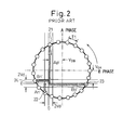
- FIG. 2 is a view for explaining an example of an operation for detection of an offset value of the conventional offset detection circuit shown in FIG. 1
- FIG. 3 is a view for explaining another example of the operation for detection of an offset value of the conventional offset detection circuit shown in FIG. 1.
- one turn of the circle expresses 360° of the A-phase or B-phase signal.
- the blank dots on the circle express the sampling times.
- the points where the one-dot-chain line ordinate and abscissa intersect the circle express the zero cross points where the offsets of the A-phase and B-phase are zero.
- the points where the vertical direction solid line 0 and horizontal direction solid line 0 intersect the circle express the zero cross points where the offsets of the A-phase and B-phase are finite values.
- the threshold value for detecting a zero cross point where a signal crosses zero is given a margin (0 ⁇ Vd).
- a sampling value detected in this range is made the phase sampling value when the signal crosses zero.
- the average value of the A-phase side absolute values of the positive value Ap' (sampling value of sampling time 21 in FIG. 2) and the negative value An' (sampling value of sampling time 22 in FIG. 2) on the B-phase side zero cross point is made the A-phase value.
- the average value of the B-phase side absolute values of the positive value Bp' (blank dot 23 in FIG. 2) and negative value Bn' (blank dot 24 in FIG. 2) on the A-phase side zero cross point is made the B-phase value.
- a conventional circuit detects each phase voltage not at the zero cross point of the A/D converted value of the other phase, but near the zero cross point (0 ⁇ Vd). For this reason, as shown in FIG. 2, when the sampling period T1 is relatively small relative to the 360° period of the input signal (one turn of the circle of FIG. 2), even if the zero cross point and sampling time become off, the amount of offset can be obtained.
- sampling period T2 when the sampling period T2 is relatively small relative to the input signal period, there are a plurality of sampling values in the range of (0 ⁇ Vd).
- sampling times 41, 42, 43, 44, 45, 46, 47, and 48 when the B-phase A/D converted value is in the range of 0 ⁇ Vd.
- the A-phase positive converted value Ap' in the case where the B-phase A/D converted value is 0+Vd is the value of the first sampling time 41 in the sampling times 41 to 44
- the A-phase positive converted value An' in the case where the B-phase A/D converted value is 0-Vd is the value of the first sampling time 45 in the sampling times 45 to 48.
- the average value of these two values ⁇ (Ap'+An')/2 ⁇ is made the offset value.
- FIG. 4A is a graph showing the A/D converted value Ap of the A-phase sampling value corresponding to the B-phase zero cross point when the B-phase offset is 0 and the A/D converted value Ap' of the A-phase sampling value corresponding to the B-phase zero cross point when the offset value is - ⁇ Ap, while FIG.
- 4B is a graph showing the A/D converted value An of the A-phase sampling value corresponding to the B-phase zero cross point when the B-phase offset is 0 and the A/D converted value Ap' of the A-phase sampling value corresponding to the B-phase zero cross point when the offset value is - ⁇ An.
- the offset values - ⁇ Ap and - ⁇ An are small, - ⁇ Ap + ( - ⁇ An ) ⁇ 0 Ap ⁇ + An ⁇ / 2 ⁇ ( Ap + An ) / 2
- the overall values become substantially equal when there is no offset.
- FIG. 5A is a graph showing the A/D converted value Ap of the A-phase sampling value corresponding to the B-phase zero cross point when the B-phase offset is 0 and the A/D converted value Ap' of the A-phase sampling value corresponding to the B-phase zero cross point when the offset value is + ⁇ Ap.
- FIG. 5B is a graph showing the A/D converted value An of the A-phase sampling value corresponding to the B-phase zero cross point and the A/D converted value An' of the A-phase sampling value corresponding to the B-phase zero cross point when the offset value + ⁇ An is relatively large. In the case shown in FIGS.
- An object of the present invention in consideration of the above prior art, is to provide an offset correction circuit of an encoder able to obtain the correct amount of offset regardless of the length of the sampling period or magnitude of the offset.
- an offset correction circuit of an encoder sampling a first phase signal and second phase signal with phases differing from each other by about 90 degrees at the same timing, converting them from an analog to digital format, and detecting an angle signal based on the obtained digital signals provided with offset detection circuits using a second phase A/D converted value of when a first phase A/D converted value is near a first value to find a second phase offset value, using a first phase A/D converted value of when a second phase A/D converted value is near a second value to find a first phase offset value, and using the currently found first offset value for the first value and the currently found second offset value for the second value when calculating the next first offset value and second offset value and correction circuits using a first offset value and second offset value to correct offsets of the first phase signal and second phase signal.
- the offset detection circuits preferably make the initial values of the first value and the second value zero.
- the offset detection circuits preferably calculate the average value of the second phase positive A/D converted value and second phase negative A/D converted value when the first phase A/D converted value is within a range set by a threshold value near the first value and detect the average value as a second phase offset value and calculate the average value of the first phase positive A/D converted value and first phase negative A/D converted value when the second phase A/D converted value is within a range set by a threshold value near the second value and detect the average value as a first phase offset value.
- the offset values are preferably values calculated from a plurality of positive A/D converted values and a plurality of negative A/D converted values.
- the positive A/D converted value and the negative A/D converted value for finding the average value are preferably alternately updated.
- correction circuits are preferably compensation circuits for subtracting from one phase A/D converted value one phase offset value found by the offset detection circuits.
- the condition for detecting the different phase voltages for obtaining the amounts of offset is fixed at "0 ⁇ Vd", but in the present invention, the conditions for detecting the different phase voltages for obtaining the amounts of offset are "X A ⁇ Vd" and "X B ⁇ Vd".
- X A , X B track the calculated offset values. Therefore, along with repeated calculations, the effect is obtained that the calculated offset values approach the correct values.
- FIG. 6 is a schematic block diagram of an offset correction circuit of an encoder according to an embodiment of the present invention.
- the offset correction circuit 60 shown by the broken line is provided with an A-phase offset detection circuit 62A, a B-phase offset detection circuit 62B, and subtraction circuits 63A and 63B.
- the A-phase signal and the B-phase signal differ in phase from each other by about 90°.
- the A-phase signal is converted by an A/D converter 61A to a digital signal A D and input to the A-phase offset detection circuit 62A and the B-phase offset detection circuit 62B.
- the B-phase signal is converted by an A/D converter 61B to a digital signal B D and input to the A-phase offset detection circuit 62A and B-phase offset detection circuit 62B.
- the A-phase offset detection circuit 62A and B-phase offset detection circuit 62B obtain the offset values Aofs and Bofs based on the A-phase and B-phase digital signals by the method described below.
- the A-phase offset detection circuit 62A uses the A-phase A/D converted value A D to find the A-phase offset value Aofs in the case where the B-phase A/D converted value B D is the value X B . Further, when calculating the next offset value Aofs, it uses the currently found offset value Bofs for the value X B .
- the B-phase offset detection circuit 62B uses the B-phase A/D converted value B D to find the B-phase offset value Bofs in the case where the A-phase A/D converted value A D is the value X A . Further, when calculating the next offset value Bofs, it uses the currently found offset value Aofs for the value X A .
- the subtraction circuits 63A and 63B are compensation circuits using the offset values detected by the offset detection circuits 62A and 62B to compensate for offsets included in the different phase A/D converted values.
- the subtraction circuit 63A receives as input the A-phase A/D converted value at its P-terminal and the A-phase offset value Aofs at its N-terminal and performs the operation (A D -Aofs).
- the subtraction circuit 63B receives as input the B-phase A/D converted value B D at its P-terminal and the B-phase offset value Bofs at its N-terminal and performs the operation (B D -Bofs).
- the subtraction circuits 63A and 63B output the offset-corrected A-phase signal and B-phase signal, then the angle detection circuit 64 detects the angle.
- the time t is 0 ⁇ t1 ⁇ t2.
- the sampling values Ap', An', Bp', and Bn' also change with each instant along with the changes in these values X A and X B .
- the initial values of the values X A and X B are preferably zero.
- the offset detection circuits calculate the average value of the B-phase positive A/D converted value B p' and B-phase negative A/D converted value B n' when the first phase A/D converted value A D is within a range set by a threshold value near the first value X A and detect the average value as a B-phase offset value. Further, they calculate the average value of the A-phase positive A/D converted value A p' and A-phase negative A/D converted value A n' when the B-phase A/D converted value B D is within a range set by a threshold value near the second value X B and detect the average value as a A-phase offset value.
- the offset values are values calculated from a plurality of positive A/D converted values and a plurality of negative A/D converted values.
- the positive A/D converted value and the negative A/D converted value for finding the average value are alternately updated.
- the subtraction circuits are compensation circuits using the offset values detected by the offset detection circuits to compensate for offsets included in the A-phase and B-phase A/D converted values.
Landscapes
- Physics & Mathematics (AREA)
- General Physics & Mathematics (AREA)
- Transmission And Conversion Of Sensor Element Output (AREA)
- Analogue/Digital Conversion (AREA)
Applications Claiming Priority (1)
| Application Number | Priority Date | Filing Date | Title |
|---|---|---|---|
| JP2006037833A JP2007218667A (ja) | 2006-02-15 | 2006-02-15 | エンコーダのオフセット補正回路 |
Publications (1)
| Publication Number | Publication Date |
|---|---|
| EP1821074A2 true EP1821074A2 (de) | 2007-08-22 |
Family
ID=38091734
Family Applications (1)
| Application Number | Title | Priority Date | Filing Date |
|---|---|---|---|
| EP07002838A Withdrawn EP1821074A2 (de) | 2006-02-15 | 2007-02-09 | Abweichungskorrekturschaltung eines Kodierers |
Country Status (4)
| Country | Link |
|---|---|
| US (1) | US20070189421A1 (de) |
| EP (1) | EP1821074A2 (de) |
| JP (1) | JP2007218667A (de) |
| CN (1) | CN101021423A (de) |
Cited By (1)
| Publication number | Priority date | Publication date | Assignee | Title |
|---|---|---|---|---|
| CN111623798A (zh) * | 2019-02-28 | 2020-09-04 | 拉碧斯半导体株式会社 | 偏移计算装置、偏移修正装置以及偏移计算方法 |
Families Citing this family (6)
| Publication number | Priority date | Publication date | Assignee | Title |
|---|---|---|---|---|
| JP5917801B2 (ja) * | 2010-03-25 | 2016-05-18 | ローム株式会社 | モータ駆動回路およびそれを用いた冷却装置、電子機器 |
| JP6235505B2 (ja) * | 2015-02-27 | 2017-11-22 | ファナック株式会社 | 自動調整機能を有するエンコーダの信号処理装置 |
| JP7748037B2 (ja) * | 2019-08-30 | 2025-10-02 | ファナック株式会社 | 数値制御装置 |
| TWI730564B (zh) | 2019-12-26 | 2021-06-11 | 財團法人工業技術研究院 | 編碼器及利用該編碼器的訊號處理方法 |
| TWI717230B (zh) * | 2020-03-12 | 2021-01-21 | 新代科技股份有限公司 | 機台編碼器安裝偏移的修正方法 |
| DE102021105880A1 (de) * | 2021-03-11 | 2022-09-15 | Infineon Technologies Ag | Drehwinkelsensorvorrichtung und Verfahren zum Bestimmen eines Drehwinkels sowie Steuervorrichtung für einen Elektromotor |
Family Cites Families (3)
| Publication number | Priority date | Publication date | Assignee | Title |
|---|---|---|---|---|
| US3705400A (en) * | 1970-12-24 | 1972-12-05 | Warner Swasey Co | Error-compensated position determining |
| JP3026949B2 (ja) * | 1997-05-12 | 2000-03-27 | ファナック株式会社 | エンコーダのオフセット補正回路 |
| US7046176B2 (en) * | 2003-04-11 | 2006-05-16 | Mitsubishi Denki Kabushiki Kaisha | Rotary encoder |
-
2006
- 2006-02-15 JP JP2006037833A patent/JP2007218667A/ja active Pending
-
2007
- 2007-02-09 EP EP07002838A patent/EP1821074A2/de not_active Withdrawn
- 2007-02-13 US US11/705,425 patent/US20070189421A1/en not_active Abandoned
- 2007-02-14 CN CNA2007100791652A patent/CN101021423A/zh active Pending
Cited By (1)
| Publication number | Priority date | Publication date | Assignee | Title |
|---|---|---|---|---|
| CN111623798A (zh) * | 2019-02-28 | 2020-09-04 | 拉碧斯半导体株式会社 | 偏移计算装置、偏移修正装置以及偏移计算方法 |
Also Published As
| Publication number | Publication date |
|---|---|
| CN101021423A (zh) | 2007-08-22 |
| JP2007218667A (ja) | 2007-08-30 |
| US20070189421A1 (en) | 2007-08-16 |
Similar Documents
| Publication | Publication Date | Title |
|---|---|---|
| EP1821074A2 (de) | Abweichungskorrekturschaltung eines Kodierers | |
| US6556153B1 (en) | System and method for improving encoder resolution | |
| US8188896B2 (en) | Digital converter for processing resolver signal | |
| US8854024B2 (en) | Power supply circuit | |
| US20110101899A1 (en) | Motor control apparatus | |
| JP4835606B2 (ja) | 回転体の位相・速度検出装置 | |
| US10389288B2 (en) | Motor controller | |
| US6215426B1 (en) | Offset correcting circuit for encoder | |
| JP5088313B2 (ja) | リニアエンコーダ信号処理装置および信号処理方法 | |
| US7826106B2 (en) | Scanning device having position correcting measuring device with connected monitoring device | |
| EP2613216B1 (de) | Halbleiterelement zur stromsteuerung und steuergerät damit | |
| US7528565B2 (en) | Signal processing device, signal processing method, signal processing program, recording medium storing the program, speed detector and servomechanism | |
| KR101012740B1 (ko) | 레졸버 디지털 변환장치 및 이를 이용한 위치 측정 장치 | |
| US20200007060A1 (en) | Motor controller | |
| US7460979B2 (en) | Method and system for enhanced resolution, automatically-calibrated position sensor | |
| CN115833687A (zh) | 基于霍尔传感器的永磁同步电机高精度转子位置拟合方法 | |
| JP4119460B2 (ja) | エンコーダの出力信号の振幅算出装置及びエンコーダの出力信号の振幅算出プログラム | |
| JP2004333156A (ja) | エンコーダ信号内挿分割器 | |
| JP2013205366A (ja) | 位置検出器 | |
| EP1752740B1 (de) | Verfahren und Schaltungsanordnung zur Interpolation des Ausgangssignals eines Kodierers | |
| EP4215878A1 (de) | Positionssensorsystem und verfahren zur fehlererkennung eines positionssensorsystems | |
| JP4508103B2 (ja) | 位置検出方法 | |
| JP3336396B2 (ja) | アブソリュートエンコーダ | |
| US10505485B2 (en) | Motor controller | |
| KR20170073351A (ko) | 모터 제어 장치 및 방법 |
Legal Events
| Date | Code | Title | Description |
|---|---|---|---|
| PUAI | Public reference made under article 153(3) epc to a published international application that has entered the european phase |
Free format text: ORIGINAL CODE: 0009012 |
|
| AK | Designated contracting states |
Kind code of ref document: A2 Designated state(s): AT BE BG CH CY CZ DE DK EE ES FI FR GB GR HU IE IS IT LI LT LU LV MC NL PL PT RO SE SI SK TR |
|
| AX | Request for extension of the european patent |
Extension state: AL BA HR MK YU |
|
| STAA | Information on the status of an ep patent application or granted ep patent |
Free format text: STATUS: THE APPLICATION HAS BEEN WITHDRAWN |
|
| 18W | Application withdrawn |
Effective date: 20080228 |