EP1814171A1 - Piezoelectric device - Google Patents
Piezoelectric device Download PDFInfo
- Publication number
- EP1814171A1 EP1814171A1 EP05799400A EP05799400A EP1814171A1 EP 1814171 A1 EP1814171 A1 EP 1814171A1 EP 05799400 A EP05799400 A EP 05799400A EP 05799400 A EP05799400 A EP 05799400A EP 1814171 A1 EP1814171 A1 EP 1814171A1
- Authority
- EP
- European Patent Office
- Prior art keywords
- vibrating reed
- seal hole
- package
- piezoelectric vibrating
- tab tape
- Prior art date
- Legal status (The legal status is an assumption and is not a legal conclusion. Google has not performed a legal analysis and makes no representation as to the accuracy of the status listed.)
- Granted
Links
Images




Classifications
-
- H—ELECTRICITY
- H10—SEMICONDUCTOR DEVICES; ELECTRIC SOLID-STATE DEVICES NOT OTHERWISE PROVIDED FOR
- H10N—ELECTRIC SOLID-STATE DEVICES NOT OTHERWISE PROVIDED FOR
- H10N30/00—Piezoelectric or electrostrictive devices
- H10N30/20—Piezoelectric or electrostrictive devices with electrical input and mechanical output, e.g. functioning as actuators or vibrators
-
- H—ELECTRICITY
- H03—ELECTRONIC CIRCUITRY
- H03H—IMPEDANCE NETWORKS, e.g. RESONANT CIRCUITS; RESONATORS
- H03H9/00—Networks comprising electromechanical or electro-acoustic elements; Electromechanical resonators
- H03H9/02—Details
- H03H9/05—Holders or supports
- H03H9/10—Mounting in enclosures
- H03H9/1007—Mounting in enclosures for bulk acoustic wave [BAW] devices
- H03H9/1014—Mounting in enclosures for bulk acoustic wave [BAW] devices the enclosure being defined by a frame built on a substrate and a cap, the frame having no mechanical contact with the BAW device
- H03H9/1021—Mounting in enclosures for bulk acoustic wave [BAW] devices the enclosure being defined by a frame built on a substrate and a cap, the frame having no mechanical contact with the BAW device the BAW device being of the cantilever type
-
- G—PHYSICS
- G01—MEASURING; TESTING
- G01C—MEASURING DISTANCES, LEVELS OR BEARINGS; SURVEYING; NAVIGATION; GYROSCOPIC INSTRUMENTS; PHOTOGRAMMETRY OR VIDEOGRAMMETRY
- G01C19/00—Gyroscopes; Turn-sensitive devices using vibrating masses; Turn-sensitive devices without moving masses; Measuring angular rate using gyroscopic effects
- G01C19/56—Turn-sensitive devices using vibrating masses, e.g. vibratory angular rate sensors based on Coriolis forces
-
- H—ELECTRICITY
- H03—ELECTRONIC CIRCUITRY
- H03H—IMPEDANCE NETWORKS, e.g. RESONANT CIRCUITS; RESONATORS
- H03H9/00—Networks comprising electromechanical or electro-acoustic elements; Electromechanical resonators
- H03H9/02—Details
- H03H9/05—Holders or supports
- H03H9/0538—Constructional combinations of supports or holders with electromechanical or other electronic elements
- H03H9/0547—Constructional combinations of supports or holders with electromechanical or other electronic elements consisting of a vertical arrangement
Definitions
- the present invention relates to a piezoelectric device, and particularly to a piezoelectric device provided with a piezoelectric vibrating reed and an IC chip that are mounted on a TAB tape.
- the piezoelectric oscillator includes a package base having a recess portion therein. Onto this recess portion, a TAB tape is mounted, in which a wiring pattern to which an IC chip and a piezoelectric vibrating reed are connected is provided on the surface of an insulation tape.
- This TAB tape is so constructed that a window portion is provided for the insulation tape and a part of the wiring pattern is bent upward through this window portion. Further, on the lower surface of the TAB tape, the IC chip is mounted, and the piezoelectric vibrating reed is mounted on the upward bent portion of the wiring pattern. Further, to the upper surface of the package base, a lid is joined, whereby the recess portion is airtightly sealed (refer to, for example, Fig. 12 in Patent Document 1.
- the piezoelectric device is a gyro sensor
- a piezoelectric vibrating reed having the following constitution.
- the piezoelectric vibrating reed of the gyro sensor is H-shaped in plane; a base portion (mount portion) connecting to a support body is provided in the center portion of the piezoelectric vibrating reed; from one end of this base portion, a pair of drive arms are protruded; and from the other end of the base portion opposed to the one end, a pair of detecting arms are protruded.
- a drive electrode is provided; and for the detection arm, a detection electrode is provided.
- These drive electrode and detection electrode conduct to an electrode pad provided for the base portion (refer to, for example, Patent Document 2).
- Patent Document 1 JP-A-2004-153408
- Patent Document 2 JP-A-2004-226181
- Fig. 8 is an explanatory view when the piezoelectric vibrating reed and the IC chip are mounted on the TAB tape.
- the TAB tape 2 In case that a piezoelectric vibrating reed 1 having the mounted portion in its center portion is mounted on a TAB tape 2 through a bump, the TAB tape 2 must have a window portion 3 as disclosed in the Patent Document 1 in the center portion of the TAB tape 2.
- an IC chip 4 is mounted on this TAB tape 2
- the TAB tape is designed so that the resonation is not produced.
- the calculation becomes very complicated in case that the IC chip is mounted on the TAB tape, so that accuracy of the calculation lowers. Therefore, the wiring pattern and the base plate resonate due to the bending vibration of the piezoelectric vibrating reed.
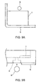
- Fig. 9 is an explanatory view of the seal hole provided in the package base.
- Fig. 9 (a) is a schematic plan view showing the seal hole provided in the package base and a mount electrode
- Fig. 9(b) is a schematic side view.
- An external electrode 6 is provided on a rear surface of the package base 5, and a mount electrode 7 for mounting a TAB tape, a piezoelectric vibrating reed and an IC chip and a circuit pattern are formed on an inner bottom surface of the package base. Further, a seal hole 8 penetrates the package base 5 linearly, so that the package outside can be confirmed visually from the package inside. Therefore, the position of the seal hole 8 in the package base 5 is limited by the position of the external electrode 6 and strength of the package. Therefore, the seal hole 8 can be provided near the mount electrode 7. However, in case that a conductive adhesive is applied onto the mount electrode 7 and the TAB tape is mounted on the mount electrode 7, the conductive adhesive frequently flows out from the mount electrode 7 and flows into the seal hole 8. In result, the conductive adhesive can flow through the seal hole 8 to the rear surface of the package base 5, which obstructs joint between the sealant 9 and the package base 5 when the seal hole 8 is melt-sealed with the sealant 9.
- An object of the invention is to provide a piezoelectric device in which miniaturization of its plane size is possible and the resonance design of a TAB tape is readily performed. Further, another object of the invention is to provide a piezoelectric device which can surely seal a seal hole.
- a piezoelectric device is characterized in that: an IC chip is mounted on an inner bottom surface of a package; a piezoelectric vibrating reed is electrically and mechanically connected onto a TAB tape in which a lead is provided on a surface of a resin tape; and the TAB tape to which the piezoelectric vibrating reed has been joined is mounted in the package, whereby the piezoelectric vibrating reed is arranged above the IC chip.
- the IC chip includes at least a circuit for driving the piezoelectric vibrating reed, and a circuit for detecting a signal outputted from the piezoelectric vibrating reed.
- the piezoelectric vibrating reed and the IC chip can be arranged up and down, the plane size of the piezoelectric device can be miniaturized. Therefore, the mounted space when the piezoelectric device is mounted on a mounting substrate can be reduced.
- the piezoelectric device is characterized in that: the TAB tape has a device hole in its center, and the lead is protruded inward of the device hole; and the leading end portion of the lead and a connection electrode provided for the piezoelectric vibrating reed are electrically and mechanically connected.
- the device hole is provided in the center portion of the TAB tape, since the IC chip is mounted on the inner bottom surface of the package, the piezoelectric vibrating reed and the IC chip can be arranged up and down, so that the plane size of the piezoelectric device can be miniaturized.
- the TAB tape is joined to only the piezoelectric vibrating reed, the elements for calculation can be reduced when the resonance design of the TAB tape is performed, so that the resonance design can be exactly performed.
- the piezoelectric device is characterized in that the piezoelectric vibrating reed has in its center a base portion on which the connection electrode is formed, and a drive arm and a detection arm for detecting an angular velocity are protruded from the base portion.
- the piezoelectric device can be functions as a gyro sensor that detects the angular velocity.
- this piezoelectric vibrating reed can be mounted in the center of the TAB tape. Therefore, the plane size of the piezoelectric device can be miniaturized.
- the piezoelectric device is characterized in that a seal hole through which the inside of the package is airtightly sealed is provided at the bottom of the package, and the seal hole has a bending portion.
- the adhesive flows out from a mount electrode and flows in the seal hole, the adhesive flows out along the side surface of the seal hole.
- the bending portion provided for the seal hole, it is possible to prevent the adhesive from flowing to the rear surface of the package.
- a sealant arranged in the seal hole melts, by the bending portion, it is possible to prevent the sealant from flowing in the inside area of the package where the IC chip or the TAB tape is arranged.
- the piezoelectric device is characterized in that: the seal hole includes an outer seal hole located on the outside of the package in relation to the bending portion, and an inner seal hole located on the inside of the package in relation to the bending portion; and the outer seal hole and the inner seal hole are separate in the horizontal direction. Since the outer seal hole and the inner seal hole are separate in the horizontal direction, it is possible to prevent the adhesive flowing out from the inner hole from directly dropping in the outer hole. Further, by the bending portion, the outflow of the adhesive can be prevented. Further, even in case that a sealant arranged in the seal hole melts, by the bending portion, it is possible to prevent the sealant from flowing in the inside area of the package where the IC chip or the TAB tape is arranged.
- Fig. 1 is an explanatory view of a piezoelectric device, in which Fig. 1 (a) is a schematic sectional view, and Fig. 1 (b) is a schematic plan view in which a lid and a TAB tape are removed.
- Fig. 2 is an explanatory view of a seal hole, in which Fig. 2 (a) is a schematic sectional view, and Fig. 2 (b) is a schematic plan view.
- Fig. 3 is an explanatory view of the TAB tape, in which Fig. 3(a) is a schematic plan view, and Fig. 3(b) is a sectional view taken along a line A-A of Fig. 3(a).
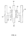
- Fig. 4 is an explanatory view of a piezoelectric vibrating reed.
- an integrated circuit (IC) chip 14 is mounted on an inner bottom surface of a package base 12
- a TAB tape 32 is mounted to which a piezoelectric vibrating reed 16 is electrically and mechanically connected, the piezoelectric vibrating reed 16 is arranged above the IC chip 14, and a lid 18 is joined onto an upper surface of the package base 12.
- the package base 12 has a recess portion 20 therein, and is formed by laminating a plane sheet and a frame sheet that are made of, for example, ceramics.
- a side surface of the recess portion 20 is formed in the shape of a staircase; and onto a bottom surface of the recess portion 20, the IC chip 14 that drives the piezoelectric vibrating reed 16 and detects a signal outputted from the piezoelectric vibrating reed 16 is mounted.
- a pad electrode 24 is provided on the upper surface of a staircase portion 22 of the recess portion 20.
- This pad electrode 24 and a pad 26 provided for the IC chip 14 are electrically connected through a wire 28, whereby the pad electrode 24 and the IC chip 14 are electrically connected.
- a part of this pad electrode 24 is electrically connected to an external electrode 30 provided on the rear surface of the package base 12.
- a mount electrode 34 for mounting the TAB tape 32 is provided on the upper surface of the stair portion 22 .
- This mount electrode 34 is electrically connected to the pad electrode 24 thereby to be electrically connected to the IC chip 14.
- the mount electrode 34 may be formed by metallize-printing metal such as tungsten on the package base 12, and thereafter performing nickel plating and gold plating. The nickel plating is performed in order to increase attachment strength between a metallized pattern and gold. Other metal plating may be used as long as it has this function.
- a seal hole 36 (36a, 36b, 36c) is provided, which penetrates the package base 12 from the recess portion 20 to the rear surface of the package base 12, and is used for airtight sealing in the package.
- This seal hole 36 is formed so that its diameter is different between the rear surface side and the inner side of the package base 12, that is, so that the hole diameter on the rear surface side of the package base 12 is larger than the hole diameter on the inner side thereof.
- a metallization 38 is applied onto an inner wall of a seal hole 36a on the rear surface side of the package base 12.
- the seal hole 36 includes a bending portion 40.
- This bending portion 40 bends horizontally seal holes 36a and 36b extending from the rear surface of the package base 12 upward, and causes a seal hole 36c to open to a side surface of the recess portion 20.
- the seal hole 36 can be formed as follows. Namely, in case the package base 12 is formed by laminating plural plane sheets and frame sheets that are made of ceramics or the like, the bottom surface of the package base 12 is formed by laminating two plane sheets, and the frame sheet is laminated on this bottom surface. At this time, in the two plane sheets, holes should be provided so that their center positions are the same and the diameter of the hole provided in the plane sheet on the rear surface side of the package base 12 becomes larger than that of the hole provided in the plane sheet on the inner side of the package base 12.
- a notch that extends from the frame inner wall that becomes the side surface of the recess portion 20 to the outer wall should be provided, and this notch can have depth by which the holes provided in the plane sheets are opened.
- the shapes of the hole and the notch are not limited to the shapes shown in Fig. 2, but they may be quadrilateral or ellipsoidal.
- the TAB tape 32 is mounted using a conductive adhesive 42.
- This TAB tape 32 is nearly rectangular, and formed by joining a lead 46 formed of copper foil onto the surface of an insulating tape 44 formed of polyimide resin or the like. Further, the TAB tape 32 has a device hole 48 in its center. This device hole 48 has such the size that a bonding tool for bonding the piezoelectric vibrating reed 16 onto the lead 46 can pass through, and the plural leads 46 are protruded from the peripheral edge of the device hole 48 to the inside of the device hole 48.
- the leads 46 are provided according to the number of connection terminals 50 provided for the piezoelectric vibrating reed 16, and extended from the position corresponding to the mount electrode 34 to the inside of the device hole 48. Further, the lead 46 provided protrusively for the device hole 48 is bent through the device hole 48 toward the insulating tape 44 side.
- the piezoelectric vibrating reed 16 is joined, using a bump 52.
- the piezoelectric vibrating reed 16 has a rectangular base portion 54 in its center, and a drive arm 56 and a detection arm 58 for detecting an angular velocity are protruded from this base portion 54.
- the piezoelectric vibrating reed 16 has a support portion 60 that protrudes from the nearly center portion of left and right sides of the base portion 54 in the left and right directions, and the drive arm 56 protrudes, in the both directions (in the up-and-down direction in Fig. 4) orthogonal to the direction along the support portion 60, from the leading portion of each support portion 60.
- the detection arm 58 protrudes in parallel to the drive arm 56 (in the up-and-down direction in Fig. 4).
- the drive arm 56 is provided with a drive electrode (not shown)
- the detection arm 58 is provided with a detection electrode (not shown)
- the drive electrode and the detection electrode conduct to a connection electrode 50.
- This connection electrode 50 provided for the base portion 54 is electrically and mechanically connected to the lead 46.
- the piezoelectric device 10 includes the piezoelectric vibrating reed 16 and the IC chip 14 in the package.
- Such the piezoelectric device 10 is used as a gyro sensor, and working of the gyro sensor is as follows. Namely, when the drive arm 56 of the piezoelectric vibrating reed 16 receives drive voltage from the IC chip 14, its leading end vibrates to the left and right (in the left and right directions in Fig. 4). At this time, when the angular velocity of rotation acts around a center of the base portion 54, the Coriolis force acts in the direction along the drive arm 56. The above vibration is transmitted through the support portion 60 and the base portion 54 to the detection arm 58, so that the detection arm 58 vibrates to the left and right (in the left and right directions in Fig. 4). An electric field on the basis of the vibration of the detection arm 58 is taken out as a signal, so that the angular velocity of rotation is detected.
- the IC chip 14 is mounted using the adhesive or the like. At this time, the IC chip 14 is mounted with its active surface faced upward, and the pad 26 provided on the active surface and the pad electrode 24 provided for the package base 12 are wire-bonded. Further, the IC chip 14 may be facedown mounted.
- the piezoelectric vibrating reed 16 is joined onto the TAB tape 32.
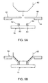
- Fig. 5 is a process drawing when the piezoelectric vibrating reed 16 is joined onto the TAB tape 32.
- the bump 52 is firstly provided on the connection electrode 50 of the piezoelectric vibrating reed 16.
- the piezoelectric vibrating reed 16 is arranged facing the connection electrode 50 upward, and the TAB tape 32 is arranged above the piezoelectric vibrating reed 16.
- the TAB tape 32 is arranged so that the connection electrode 50 of the piezoelectric vibrating reed 16 and the leading end of the TAB tape 32 are superimposed on each other.
- the bonding tool 62 is arranged (refer to Fig. 5(a)). Thereafter, the bonding tool 62 is caused to descend, whereby the lead 46 of the TAB tape 32 is bent by the bonding tool 62, and the leading end of the lead 46 is joined to the connection electrode 50 of the piezoelectric vibrating reed 16 (refer to Fig. 5(b)). At this time, in case that the lead 46 is joined to the piezoelectric vibrating reed 16 by heat-press bonding, the joint portion is heated and the leading end of the lead 46 should be pressed on the bump 52 by the bonding tool 62.
- the ultrasonic vibration should be applied to the bonding tool 62 thereby to join an interface between the lead 46 and the bump 52.
- the TAB tape 32 to which the piezoelectric vibrating reed 16 has been joined is mounted onto the mount electrode 34.
- the conductive adhesive 42 such as silver paste
- the lid 18 for sealing the recess portion 20 of the package base 12 is joined onto the upper surface of the package base 12.
- the lid 18 is made of, for example, metal
- the lid may be joined onto the package base 12 by seam welding or the like.
- sealant 64 is a metal ball formed of gold-tin soldered material or lead-tin soldered material. Further, as the material of the sealant 64, other materials than the above material may be used, for example, Sn soldered material, silver-copper alloy, or brazing filler metal. Further, the shape of the sealant 64 may be other shapes than the above shape, for example, a disk. Further, hole-sealing is specifically performed as follows. Firstly, the piezoelectric device 10 before hole-sealing is laid in vacuum, and the sealant 64 is set in the opening portion of the seal hole 36 (refer to Fig. 2(a)).
- the sealant 64 is set in the seal hole 36a on the rear surface side of the package base 12, it is possible to prevent the sealant 64 from moving by the side surface of the seal hole 36a on the rear surface side of the package base 12. Thereafter, the sealant 64 is irradiated with electronic beam or laser beam, or brought into contact with a heating device, thereby to be melted. The melted sealant 64 is attached to the metallization 38, whereby the seal hole 36 is sealed. Therefore, the recess portion 20 is vacuum-sealed.
- the piezoelectric device 10 is forwarded as a gyro sensor.
- the piezoelectric vibrating reed 16 is arranged above the IC chip 14. Therefore, even under the construction in which the connection electrode 50 is formed in the center portion of the piezoelectric vibrating reed 16, and this connection electrode 50 and the reed 46 of the TAB tape 32 are electrically and mechanically connected, the plane size of the piezoelectric device 10 can be miniaturized. In result, the mounted space when the piezoelectric device 10 is mounted on the mounting substrate can be reduced.
- the piezoelectric device 10 since the IC chip 14 is not mounted on the TAB tape 32, the number of elements for calculation when the resonance design of the TAB tape 32 is performed can be reduced, so that the resonance design can be exactly performed. Therefore, the piezoelectric device 10 of high accuracy can be obtained.
- the IC chip 14 is mounted on the package base 12, the strength of the TAB tape 32 is not short. Therefore, the piezoelectric device 10 of high reliability can be obtained. Further, if the IC chip is mounted on the TAB tape, the mass added to the TAB tape becomes large, so that the strength of the TAB tape is short.
- the seal hole 36 provided for the package base 12 has the bending portion 40, even if the conductive adhesive 42 applied on the mount electrode 34 flows out when the TAB tape 32 is joined onto the mount electrode 34, the outflow of the conductive adhesive 42 can be prevented by the bending portion 40. Namely, the conductive adhesive 42 does not flow out from the bending portion 40 to the rear surface side of the package base 12. Therefore, the mount electrode 34 and the metallization 38 applied onto the seal hole 36 do not short. Further, since the metallization 38 is not covered with the conductive adhesive 42 that has flown out, the seal hole 36 can be surely sealed by the sealant 64. Hereby, the piezoelectric deice 10 of high reliability can be obtained.
- the piezoelectric vibrating reed 16 is not limited to the above mode, but may be formed in the shape shown in Fig. 6. Namely, a piezoelectric vibrating reed 70 can be so constructed that: a base portion 72 is provided in its center portion; a pair of drive arms 74 protrude from one side of this base portion 72; and a pair of detection arms 76 protrude from the opposite side to the above side. In Fig. 6, a connection electrode, a drive electrode, and a detection electrode are omitted.
- the piezoelectric vibrating reed 16 may be a tuning fork type piezoelectric vibrating reed in which a pair of vibration arms is protruded from a base portion. Further, the piezoelectric vibrating reed 16 may be a piezoelectric vibrating reed such as AT-cut or an elastic surface wave resonance reed and the like. Further, the piezoelectric device 10 is not limited to the gyro sensor, but may be applied to a piezoelectric oscillator or an elastic surface wave oscillator.
- Fig. 7 (a) is a schematic sectional view of the seal hole
- Fig. 7 (b) is a schematic plan view of the seal hole.
- This seal hole 80 penetrates the package base 12 from the rear surface of the package base 12 to the upper surface of the staircase portion 22 of the package base 12, extends from the rear surface of the package base 12 upward, bends in the horizontal direction on the way, and thereafter extends again upward.
- a seal hole 80a extending from the rear surface side of the package 12 upward has the two-stage structure, and the hole diameter on the rear surface side is formed wider than the inner hole diameter.
- a metallization 84 is applied onto the inner wall of the hole located on this rear surface side.
- the upper end of this seal hole 80a opens to a seal hole 80b extending horizontally.
- This seal hole 80b functions as a bending portion 82.
- This seal hole 80b is connected to a seal hole 80c extending from the upper surface of the seal hole 80b to the upper surface of the staircase portion 22 of the package base 12.
- the seal hole 80a on the rear surface side of the package base 12 (outer seal hole located on the outside of the package in relation to the bending portion 82) and the seal hole 80c on the staircase portion 22 side (inner seal hole located on the inside of the package in relation to the bending portion 82) are separate from each other by the desired distance in the horizontal direction.
- This desired distance is a distance in which the seal hole 80c and the seal hole 80a are not superimposed on each other up and down, that is, a distance in which the seal hole 80a is not seen in the hole of the seal hole 80c when the seal hole 80c is seen from the upside.
- the rear surface of the IC chip and the metallization 84 of the seal hole 80 do not short, and a recess portion of the package base 12 can be surely sealed airtightly. Further, when a sealant provided for the seal hole 80 melts, it is possible to prevent by the seal hole 80b (bending portion 82) the sealant from flowing from the seal hole 80a into the portion on which the IC chip is mounted and the portion on which the TAB tape is mounted.
Landscapes
- Physics & Mathematics (AREA)
- Acoustics & Sound (AREA)
- Engineering & Computer Science (AREA)
- General Physics & Mathematics (AREA)
- Radar, Positioning & Navigation (AREA)
- Remote Sensing (AREA)
- Piezo-Electric Or Mechanical Vibrators, Or Delay Or Filter Circuits (AREA)
- Gyroscopes (AREA)
- Oscillators With Electromechanical Resonators (AREA)
Abstract

Description
- The present invention relates to a piezoelectric device, and particularly to a piezoelectric device provided with a piezoelectric vibrating reed and an IC chip that are mounted on a TAB tape.
- As piezoelectric devices, there are a gyro sensor for detecting an angular velocity, a piezoelectric vibrator and a piezoelectric oscillator that output the desired oscillation frequency, and a filter that selects the desired frequency band. As this piezoelectric device, there is, for example, a piezoelectric oscillator having the following constitution. Namely, the piezoelectric oscillator includes a package base having a recess portion therein. Onto this recess portion, a TAB tape is mounted, in which a wiring pattern to which an IC chip and a piezoelectric vibrating reed are connected is provided on the surface of an insulation tape. This TAB tape is so constructed that a window portion is provided for the insulation tape and a part of the wiring pattern is bent upward through this window portion. Further, on the lower surface of the TAB tape, the IC chip is mounted, and the piezoelectric vibrating reed is mounted on the upward bent portion of the wiring pattern. Further, to the upper surface of the package base, a lid is joined, whereby the recess portion is airtightly sealed (refer to, for example, Fig. 12 in
Patent Document 1. - Further, in case that the piezoelectric device is a gyro sensor, there is, for example, a piezoelectric vibrating reed having the following constitution. Namely, the piezoelectric vibrating reed of the gyro sensor is H-shaped in plane; a base portion (mount portion) connecting to a support body is provided in the center portion of the piezoelectric vibrating reed; from one end of this base portion, a pair of drive arms are protruded; and from the other end of the base portion opposed to the one end, a pair of detecting arms are protruded. For the drive arm, a drive electrode is provided; and for the detection arm, a detection electrode is provided. These drive electrode and detection electrode conduct to an electrode pad provided for the base portion (refer to, for example, Patent Document 2).
[Patent Document 1]JP-A-2004-153408
[Patent Document 2]JP-A-2004-226181 - Fig. 8 is an explanatory view when the piezoelectric vibrating reed and the IC chip are mounted on the TAB tape. In case that a piezoelectric vibrating
reed 1 having the mounted portion in its center portion is mounted on aTAB tape 2 through a bump, theTAB tape 2 must have awindow portion 3 as disclosed in thePatent Document 1 in the center portion of theTAB tape 2. In case that anIC chip 4 is mounted on thisTAB tape 2, it cannot be mounted under the piezoelectric vibratingreed 1 because thewindow portion 3 is provided. Therefore, theTAB tape 2 is extended to the side, and theIC chip 4 is mounted on this extended portion. However, with miniaturization of an electronic apparatus on which the piezoelectric device is mounted, it is recently necessary to reduce the thickness and the plane size of the piezoelectric device. Therefore, in the above constitution, the plane size of the piezoelectric device becomes large and the miniaturization cannot be achieved, so that the mounted space of the piezoelectric device becomes large. - Further, in case of the gyro sensor in which the piezoelectric vibrating reed is mounted on the TAB tape, there is possibility that the wiring pattern of the TAB tape and the base plate thereof resonate due to bending vibration of the piezoelectric vibrating reed. Therefore, the TAB tape is designed so that the resonation is not produced. Though such the resonation design is obtained by calculation, the calculation becomes very complicated in case that the IC chip is mounted on the TAB tape, so that accuracy of the calculation lowers. Therefore, the wiring pattern and the base plate resonate due to the bending vibration of the piezoelectric vibrating reed.
- Further, in the piezoelectric device, its package inside is airtightly sealed in an atmosphere of vacuum or inert gas. As an airtight sealing method, there is a method of joining a lid onto the upper surface of a package base having a seal hole on the bottom surface, and thereafter melt-sealing the seal hole with a sealant while putting the package in vacuum. Fig. 9 is an explanatory view of the seal hole provided in the package base. Fig. 9 (a) is a schematic plan view showing the seal hole provided in the package base and a mount electrode, and Fig. 9(b) is a schematic side view. An
external electrode 6 is provided on a rear surface of thepackage base 5, and amount electrode 7 for mounting a TAB tape, a piezoelectric vibrating reed and an IC chip and a circuit pattern are formed on an inner bottom surface of the package base. Further, aseal hole 8 penetrates thepackage base 5 linearly, so that the package outside can be confirmed visually from the package inside. Therefore, the position of theseal hole 8 in thepackage base 5 is limited by the position of theexternal electrode 6 and strength of the package. Therefore, theseal hole 8 can be provided near themount electrode 7. However, in case that a conductive adhesive is applied onto themount electrode 7 and the TAB tape is mounted on themount electrode 7, the conductive adhesive frequently flows out from themount electrode 7 and flows into theseal hole 8. In result, the conductive adhesive can flow through theseal hole 8 to the rear surface of thepackage base 5, which obstructs joint between the sealant 9 and thepackage base 5 when theseal hole 8 is melt-sealed with the sealant 9. - An object of the invention is to provide a piezoelectric device in which miniaturization of its plane size is possible and the resonance design of a TAB tape is readily performed. Further, another object of the invention is to provide a piezoelectric device which can surely seal a seal hole.
- In order to achieve the above objects, a piezoelectric device according to the invention is characterized in that: an IC chip is mounted on an inner bottom surface of a package; a piezoelectric vibrating reed is electrically and mechanically connected onto a TAB tape in which a lead is provided on a surface of a resin tape; and the TAB tape to which the piezoelectric vibrating reed has been joined is mounted in the package, whereby the piezoelectric vibrating reed is arranged above the IC chip. In this case, the IC chip includes at least a circuit for driving the piezoelectric vibrating reed, and a circuit for detecting a signal outputted from the piezoelectric vibrating reed. Since the piezoelectric vibrating reed and the IC chip can be arranged up and down, the plane size of the piezoelectric device can be miniaturized. Therefore, the mounted space when the piezoelectric device is mounted on a mounting substrate can be reduced.
- Further, the piezoelectric device is characterized in that: the TAB tape has a device hole in its center, and the lead is protruded inward of the device hole; and the leading end portion of the lead and a connection electrode provided for the piezoelectric vibrating reed are electrically and mechanically connected. Even in case that the device hole is provided in the center portion of the TAB tape, since the IC chip is mounted on the inner bottom surface of the package, the piezoelectric vibrating reed and the IC chip can be arranged up and down, so that the plane size of the piezoelectric device can be miniaturized. Further, since the TAB tape is joined to only the piezoelectric vibrating reed, the elements for calculation can be reduced when the resonance design of the TAB tape is performed, so that the resonance design can be exactly performed.
- Further, the piezoelectric device is characterized in that the piezoelectric vibrating reed has in its center a base portion on which the connection electrode is formed, and a drive arm and a detection arm for detecting an angular velocity are protruded from the base portion. Hereby, the piezoelectric device can be functions as a gyro sensor that detects the angular velocity. Further, even in case that the piezoelectric vibrating reed has the base portion in its center, this piezoelectric vibrating reed can be mounted in the center of the TAB tape. Therefore, the plane size of the piezoelectric device can be miniaturized.
- Further, the piezoelectric device is characterized in that a seal hole through which the inside of the package is airtightly sealed is provided at the bottom of the package, and the seal hole has a bending portion. In case that an adhesive flows out from a mount electrode and flows in the seal hole, the adhesive flows out along the side surface of the seal hole. However, by the bending portion provided for the seal hole, it is possible to prevent the adhesive from flowing to the rear surface of the package. Further, even in case that a sealant arranged in the seal hole melts, by the bending portion, it is possible to prevent the sealant from flowing in the inside area of the package where the IC chip or the TAB tape is arranged.
- Further, the piezoelectric device is characterized in that: the seal hole includes an outer seal hole located on the outside of the package in relation to the bending portion, and an inner seal hole located on the inside of the package in relation to the bending portion; and the outer seal hole and the inner seal hole are separate in the horizontal direction. Since the outer seal hole and the inner seal hole are separate in the horizontal direction, it is possible to prevent the adhesive flowing out from the inner hole from directly dropping in the outer hole. Further, by the bending portion, the outflow of the adhesive can be prevented. Further, even in case that a sealant arranged in the seal hole melts, by the bending portion, it is possible to prevent the sealant from flowing in the inside area of the package where the IC chip or the TAB tape is arranged.
-
- Fig. 1 is an explanatory view of a piezoelectric device.
- Fig. 2 is an explanatory view of a seal hole.
- Fig. 3 is an explanatory view of a TAB tape.
- Fig. 4 is an explanatory view of a piezoelectric vibrating reed.
- Fig. 5 is a process drawing when the piezoelectric vibrating reed is joined onto the TAB tape.
- Fig. 6 is an explanatory view of a modified example of the piezoelectric vibrating reed.
- Fig. 7 is an explanatory view of a modified example of the seal hole.
- Fig. 8 is an explanatory view when a piezoelectric vibrating reed and an IC chip are mounted on a TAB tape in the related art.
- Fig. 9 is an explanatory view of a seal hole provided for a package base in the related art.
- A best mode of a piezoelectric device will be described below. Fig. 1 is an explanatory view of a piezoelectric device, in which Fig. 1 (a) is a schematic sectional view, and Fig. 1 (b) is a schematic plan view in which a lid and a TAB tape are removed. Fig. 2 is an explanatory view of a seal hole, in which Fig. 2 (a) is a schematic sectional view, and Fig. 2 (b) is a schematic plan view. Fig. 3 is an explanatory view of the TAB tape, in which Fig. 3(a) is a schematic plan view, and Fig. 3(b) is a sectional view taken along a line A-A of Fig. 3(a). Fig. 4 is an explanatory view of a piezoelectric vibrating reed. In the constitution of a
piezoelectric device 10, an integrated circuit (IC)chip 14 is mounted on an inner bottom surface of apackage base 12, aTAB tape 32 is mounted to which apiezoelectric vibrating reed 16 is electrically and mechanically connected, the piezoelectric vibratingreed 16 is arranged above theIC chip 14, and alid 18 is joined onto an upper surface of thepackage base 12. - The
package base 12 has arecess portion 20 therein, and is formed by laminating a plane sheet and a frame sheet that are made of, for example, ceramics. A side surface of therecess portion 20 is formed in the shape of a staircase; and onto a bottom surface of therecess portion 20, theIC chip 14 that drives the piezoelectric vibratingreed 16 and detects a signal outputted from the piezoelectric vibratingreed 16 is mounted. - Further, on the upper surface of a
staircase portion 22 of therecess portion 20, apad electrode 24 is provided. Thispad electrode 24 and apad 26 provided for theIC chip 14 are electrically connected through awire 28, whereby thepad electrode 24 and theIC chip 14 are electrically connected. A part of thispad electrode 24 is electrically connected to anexternal electrode 30 provided on the rear surface of thepackage base 12. Further, on the upper surface of thestair portion 22, amount electrode 34 for mounting theTAB tape 32 is provided. Thismount electrode 34 is electrically connected to thepad electrode 24 thereby to be electrically connected to theIC chip 14. Themount electrode 34 may be formed by metallize-printing metal such as tungsten on thepackage base 12, and thereafter performing nickel plating and gold plating. The nickel plating is performed in order to increase attachment strength between a metallized pattern and gold. Other metal plating may be used as long as it has this function. - Further, in the
package base 12, a seal hole 36 (36a, 36b, 36c) is provided, which penetrates thepackage base 12 from therecess portion 20 to the rear surface of thepackage base 12, and is used for airtight sealing in the package. Thisseal hole 36 is formed so that its diameter is different between the rear surface side and the inner side of thepackage base 12, that is, so that the hole diameter on the rear surface side of thepackage base 12 is larger than the hole diameter on the inner side thereof. Further, ametallization 38 is applied onto an inner wall of aseal hole 36a on the rear surface side of thepackage base 12. Further, theseal hole 36 includes a bendingportion 40. This bendingportion 40 bends horizontally sealholes package base 12 upward, and causes aseal hole 36c to open to a side surface of therecess portion 20. Theseal hole 36 can be formed as follows. Namely, in case thepackage base 12 is formed by laminating plural plane sheets and frame sheets that are made of ceramics or the like, the bottom surface of thepackage base 12 is formed by laminating two plane sheets, and the frame sheet is laminated on this bottom surface. At this time, in the two plane sheets, holes should be provided so that their center positions are the same and the diameter of the hole provided in the plane sheet on the rear surface side of thepackage base 12 becomes larger than that of the hole provided in the plane sheet on the inner side of thepackage base 12. Further, in the frame sheet, a notch that extends from the frame inner wall that becomes the side surface of therecess portion 20 to the outer wall should be provided, and this notch can have depth by which the holes provided in the plane sheets are opened. Further, the shapes of the hole and the notch are not limited to the shapes shown in Fig. 2, but they may be quadrilateral or ellipsoidal. - On the
mount electrode 34, theTAB tape 32 is mounted using aconductive adhesive 42. ThisTAB tape 32 is nearly rectangular, and formed by joining a lead 46 formed of copper foil onto the surface of an insulatingtape 44 formed of polyimide resin or the like. Further, theTAB tape 32 has adevice hole 48 in its center. Thisdevice hole 48 has such the size that a bonding tool for bonding thepiezoelectric vibrating reed 16 onto thelead 46 can pass through, and the plural leads 46 are protruded from the peripheral edge of thedevice hole 48 to the inside of thedevice hole 48. The leads 46 are provided according to the number ofconnection terminals 50 provided for the piezoelectric vibratingreed 16, and extended from the position corresponding to themount electrode 34 to the inside of thedevice hole 48. Further, thelead 46 provided protrusively for thedevice hole 48 is bent through thedevice hole 48 toward the insulatingtape 44 side. - To a leading end of this
lead 46, the piezoelectric vibratingreed 16 is joined, using abump 52. The piezoelectric vibratingreed 16 has arectangular base portion 54 in its center, and adrive arm 56 and adetection arm 58 for detecting an angular velocity are protruded from thisbase portion 54. Specifically, the piezoelectric vibratingreed 16 has asupport portion 60 that protrudes from the nearly center portion of left and right sides of thebase portion 54 in the left and right directions, and thedrive arm 56 protrudes, in the both directions (in the up-and-down direction in Fig. 4) orthogonal to the direction along thesupport portion 60, from the leading portion of eachsupport portion 60. Further, from the nearly center portion of up-and-down sides of thebase portion 54, thedetection arm 58 protrudes in parallel to the drive arm 56 (in the up-and-down direction in Fig. 4). Thedrive arm 56 is provided with a drive electrode (not shown), thedetection arm 58 is provided with a detection electrode (not shown), and the drive electrode and the detection electrode conduct to aconnection electrode 50. Thisconnection electrode 50 provided for thebase portion 54 is electrically and mechanically connected to thelead 46. - Onto the upper surface of the
package base 12, thelid 18 is joined. Hereby, thepiezoelectric device 10 includes the piezoelectric vibratingreed 16 and theIC chip 14 in the package. - Such the
piezoelectric device 10 is used as a gyro sensor, and working of the gyro sensor is as follows. Namely, when thedrive arm 56 of the piezoelectric vibratingreed 16 receives drive voltage from theIC chip 14, its leading end vibrates to the left and right (in the left and right directions in Fig. 4). At this time, when the angular velocity of rotation acts around a center of thebase portion 54, the Coriolis force acts in the direction along thedrive arm 56. The above vibration is transmitted through thesupport portion 60 and thebase portion 54 to thedetection arm 58, so that thedetection arm 58 vibrates to the left and right (in the left and right directions in Fig. 4). An electric field on the basis of the vibration of thedetection arm 58 is taken out as a signal, so that the angular velocity of rotation is detected. - Next, a manufacturing method of the
piezoelectric device 10 will be described. Firstly, on therecess portion 20 bottom surface of thepackage base 12, theIC chip 14 is mounted using the adhesive or the like. At this time, theIC chip 14 is mounted with its active surface faced upward, and thepad 26 provided on the active surface and thepad electrode 24 provided for thepackage base 12 are wire-bonded. Further, theIC chip 14 may be facedown mounted. - Further, the piezoelectric vibrating
reed 16 is joined onto theTAB tape 32. Fig. 5 is a process drawing when the piezoelectric vibratingreed 16 is joined onto theTAB tape 32. Specifically, thebump 52 is firstly provided on theconnection electrode 50 of the piezoelectric vibratingreed 16. The piezoelectric vibratingreed 16 is arranged facing theconnection electrode 50 upward, and theTAB tape 32 is arranged above the piezoelectric vibratingreed 16. At this time, theTAB tape 32 is arranged so that theconnection electrode 50 of the piezoelectric vibratingreed 16 and the leading end of theTAB tape 32 are superimposed on each other. Next, above thedevice hole 48 of theTAB tape 32, thebonding tool 62 is arranged (refer to Fig. 5(a)). Thereafter, thebonding tool 62 is caused to descend, whereby thelead 46 of theTAB tape 32 is bent by thebonding tool 62, and the leading end of thelead 46 is joined to theconnection electrode 50 of the piezoelectric vibrating reed 16 (refer to Fig. 5(b)). At this time, in case that thelead 46 is joined to the piezoelectric vibratingreed 16 by heat-press bonding, the joint portion is heated and the leading end of thelead 46 should be pressed on thebump 52 by thebonding tool 62. Further, in case that thelead 46 is joined to the piezoelectric vibratingreed 16 by ultrasonic vibration, when the leading end of thelead 46 is pressed on thebump 52 by thebonding tool 62, the ultrasonic vibration should be applied to thebonding tool 62 thereby to join an interface between the lead 46 and thebump 52. - Thereafter, on the
package base 12 on which theIC chip 14 has been mounted, theTAB tape 32 to which thepiezoelectric vibrating reed 16 has been joined is mounted. At this time, onto themount electrode 34, by use of the conductive adhesive 42 such as silver paste, thelead 46 of theTAB tape 32 is joined. Hereby, the piezoelectric vibratingreed 16 and theIC chip 14 are electrically connected. - Next, onto the upper surface of the
package base 12, thelid 18 for sealing therecess portion 20 of thepackage base 12 is joined. In case that thelid 18 is made of, for example, metal, the lid may be joined onto thepackage base 12 by seam welding or the like. - Thereafter, the
seal hole 36 provided on the bottom surface of thepackage base 12 is airtightly sealed by asealant 64. Thissealant 64 is a metal ball formed of gold-tin soldered material or lead-tin soldered material. Further, as the material of thesealant 64, other materials than the above material may be used, for example, Sn soldered material, silver-copper alloy, or brazing filler metal. Further, the shape of thesealant 64 may be other shapes than the above shape, for example, a disk. Further, hole-sealing is specifically performed as follows. Firstly, thepiezoelectric device 10 before hole-sealing is laid in vacuum, and thesealant 64 is set in the opening portion of the seal hole 36 (refer to Fig. 2(a)). Since the diameter of theseal hole 36a on the rear surface side of thepackage base 12 is larger than the diameter of theinner seal hole 36b, when thesealant 64 is set in theseal hole 36a on the rear surface side of thepackage base 12, it is possible to prevent thesealant 64 from moving by the side surface of theseal hole 36a on the rear surface side of thepackage base 12. Thereafter, thesealant 64 is irradiated with electronic beam or laser beam, or brought into contact with a heating device, thereby to be melted. The meltedsealant 64 is attached to themetallization 38, whereby theseal hole 36 is sealed. Therefore, therecess portion 20 is vacuum-sealed. - Thereafter, a probe is brought into contact with the
external electrode 30 and the like, and data such as an amplification factor for controlling detection sensitivity of the piezoelectric vibratingreed 16 is written into theIC chip 14. After a characteristic test, thepiezoelectric device 10 is forwarded as a gyro sensor. - In the construction of such the
piezoelectric device 10, since theIC chip 14 is mounted on therecess portion 20 bottom surface of thepackage base 12, and theTAB tape 32 is mounted on the upper surface of thestaircase portion 22 in therecess portion 20, the piezoelectric vibratingreed 16 is arranged above theIC chip 14. Therefore, even under the construction in which theconnection electrode 50 is formed in the center portion of the piezoelectric vibratingreed 16, and thisconnection electrode 50 and thereed 46 of theTAB tape 32 are electrically and mechanically connected, the plane size of thepiezoelectric device 10 can be miniaturized. In result, the mounted space when thepiezoelectric device 10 is mounted on the mounting substrate can be reduced. - Further, in the
piezoelectric device 10, since theIC chip 14 is not mounted on theTAB tape 32, the number of elements for calculation when the resonance design of theTAB tape 32 is performed can be reduced, so that the resonance design can be exactly performed. Therefore, thepiezoelectric device 10 of high accuracy can be obtained. - Further, the
IC chip 14 is mounted on thepackage base 12, the strength of theTAB tape 32 is not short. Therefore, thepiezoelectric device 10 of high reliability can be obtained. Further, if the IC chip is mounted on the TAB tape, the mass added to the TAB tape becomes large, so that the strength of the TAB tape is short. - Further, since the
seal hole 36 provided for thepackage base 12 has the bendingportion 40, even if the conductive adhesive 42 applied on themount electrode 34 flows out when theTAB tape 32 is joined onto themount electrode 34, the outflow of the conductive adhesive 42 can be prevented by the bendingportion 40. Namely, theconductive adhesive 42 does not flow out from the bendingportion 40 to the rear surface side of thepackage base 12. Therefore, themount electrode 34 and themetallization 38 applied onto theseal hole 36 do not short. Further, since themetallization 38 is not covered with the conductive adhesive 42 that has flown out, theseal hole 36 can be surely sealed by thesealant 64. Hereby, thepiezoelectric deice 10 of high reliability can be obtained. - Further, when the
sealant 64 melts, it is possible to prevent by the bendingportion 40 the sealant from flowing from theseal hole 36 into the portion on which theIC chip 14 is mounted and the portion on which theTAB tape 32 is mounted. - The piezoelectric vibrating
reed 16 is not limited to the above mode, but may be formed in the shape shown in Fig. 6. Namely, a piezoelectric vibratingreed 70 can be so constructed that: abase portion 72 is provided in its center portion; a pair ofdrive arms 74 protrude from one side of thisbase portion 72; and a pair ofdetection arms 76 protrude from the opposite side to the above side. In Fig. 6, a connection electrode, a drive electrode, and a detection electrode are omitted. - Further, the piezoelectric vibrating
reed 16 may be a tuning fork type piezoelectric vibrating reed in which a pair of vibration arms is protruded from a base portion. Further, the piezoelectric vibratingreed 16 may be a piezoelectric vibrating reed such as AT-cut or an elastic surface wave resonance reed and the like. Further, thepiezoelectric device 10 is not limited to the gyro sensor, but may be applied to a piezoelectric oscillator or an elastic surface wave oscillator. - Further, the shape of the
seal hole 64 is not limited to the above shape, but may be the shape shown in Fig. 7. Here, Fig. 7 (a) is a schematic sectional view of the seal hole, and Fig. 7 (b) is a schematic plan view of the seal hole. Thisseal hole 80 penetrates thepackage base 12 from the rear surface of thepackage base 12 to the upper surface of thestaircase portion 22 of thepackage base 12, extends from the rear surface of thepackage base 12 upward, bends in the horizontal direction on the way, and thereafter extends again upward. Aseal hole 80a extending from the rear surface side of thepackage 12 upward has the two-stage structure, and the hole diameter on the rear surface side is formed wider than the inner hole diameter. Onto the inner wall of the hole located on this rear surface side, ametallization 84 is applied. The upper end of thisseal hole 80a opens to aseal hole 80b extending horizontally. Thisseal hole 80b functions as a bendingportion 82. Thisseal hole 80b is connected to aseal hole 80c extending from the upper surface of theseal hole 80b to the upper surface of thestaircase portion 22 of thepackage base 12. Theseal hole 80a on the rear surface side of the package base 12 (outer seal hole located on the outside of the package in relation to the bending portion 82) and theseal hole 80c on thestaircase portion 22 side (inner seal hole located on the inside of the package in relation to the bending portion 82) are separate from each other by the desired distance in the horizontal direction. This desired distance is a distance in which theseal hole 80c and theseal hole 80a are not superimposed on each other up and down, that is, a distance in which theseal hole 80a is not seen in the hole of theseal hole 80c when theseal hole 80c is seen from the upside. By such theseal hole 80, even in case that the conductive adhesive is used when the IC chip is joined to thepackage base 12, this conductive adhesive never flow in theseal hole 80. Further, even if the conductive adhesive applied onto the mount electrode flows into theseal hole 80c, theseal hole 80b extending horizontally prevents the conductive adhesive from directly dropping from theseal hole 80c to theseal hole 80a. Therefore, the rear surface of the IC chip and themetallization 84 of theseal hole 80 do not short, and a recess portion of thepackage base 12 can be surely sealed airtightly. Further, when a sealant provided for theseal hole 80 melts, it is possible to prevent by theseal hole 80b (bending portion 82) the sealant from flowing from theseal hole 80a into the portion on which the IC chip is mounted and the portion on which the TAB tape is mounted.
Claims (5)
- A piezoelectric device characterized in that:an IC chip is mounted on an inner bottom surface of a package;a piezoelectric vibrating reed is electrically and mechanically connected onto a TAB tape in which a lead is provided on a surface of a resin tape; andthe TAB tape to which the piezoelectric vibrating reed has been joined is mounted in the package, whereby the piezoelectric vibrating reed is arranged above the IC chip.
- The piezoelectric device according to Claim 1, characterized in that:the TAB tape has a device hole in its center, and the lead is protruded inward of the device hole; andthe leading end portion of the lead and a connection electrode provided for the piezoelectric vibrating reed are electrically and mechanically connected.
- The piezoelectric device according to Claim 2, characterized in that the piezoelectric vibrating reed has in its center a base portion on which the connection electrode is formed, and a drive arm and a detection arm for detecting an angular velocity are protruded from the base portion.
- The piezoelectric device according to Claim 1, characterized in that a seal hole through which the inside of the package is airtightly sealed is provided at the bottom of the package, and the seal hole has a bending portion.
- The piezoelectric device according to Claim 4, characterized in that:the seal hole includes an outer seal hole located on the outside of the package in relation to the bending portion, and an inner seal hole located on the inside of the package in relation to the bending portion; andthe outer seal hole and the inner seal hole are separate in the horizontal direction.
Applications Claiming Priority (2)
| Application Number | Priority Date | Filing Date | Title |
|---|---|---|---|
| JP2004304802 | 2004-10-19 | ||
| PCT/JP2005/019649 WO2006043713A1 (en) | 2004-10-19 | 2005-10-19 | Piezoelectric device |
Publications (3)
| Publication Number | Publication Date |
|---|---|
| EP1814171A1 true EP1814171A1 (en) | 2007-08-01 |
| EP1814171A4 EP1814171A4 (en) | 2011-02-02 |
| EP1814171B1 EP1814171B1 (en) | 2012-06-13 |
Family
ID=36180051
Family Applications (1)
| Application Number | Title | Priority Date | Filing Date |
|---|---|---|---|
| EP20050799400 Expired - Lifetime EP1814171B1 (en) | 2004-10-19 | 2005-10-19 | Piezoelectric device |
Country Status (6)
| Country | Link |
|---|---|
| US (1) | US7157836B2 (en) |
| EP (1) | EP1814171B1 (en) |
| JP (1) | JP4873310B2 (en) |
| KR (1) | KR100869201B1 (en) |
| CN (1) | CN101044639A (en) |
| WO (1) | WO2006043713A1 (en) |
Families Citing this family (32)
| Publication number | Priority date | Publication date | Assignee | Title |
|---|---|---|---|---|
| JP3841304B2 (en) * | 2004-02-17 | 2006-11-01 | セイコーエプソン株式会社 | Piezoelectric oscillator and manufacturing method thereof |
| DE102005008514B4 (en) * | 2005-02-24 | 2019-05-16 | Tdk Corporation | Microphone membrane and microphone with the microphone membrane |
| DE102005008511B4 (en) | 2005-02-24 | 2019-09-12 | Tdk Corporation | MEMS microphone |
| JP4554398B2 (en) * | 2005-03-03 | 2010-09-29 | セイコーエプソン株式会社 | Surface acoustic wave device and method for manufacturing surface acoustic wave device |
| US7528529B2 (en) | 2005-10-17 | 2009-05-05 | Semiconductor Energy Laboratory Co., Ltd. | Micro electro mechanical system, semiconductor device, and manufacturing method thereof |
| DE102005050398A1 (en) * | 2005-10-20 | 2007-04-26 | Epcos Ag | Cavity housing for a mechanically sensitive electronic device and method of manufacture |
| WO2007055133A1 (en) * | 2005-11-08 | 2007-05-18 | Matsushita Electric Industrial Co., Ltd. | Angular velocity sensor and process for producing the same |
| DE102005053765B4 (en) * | 2005-11-10 | 2016-04-14 | Epcos Ag | MEMS package and method of manufacture |
| JP4240053B2 (en) * | 2006-04-24 | 2009-03-18 | エプソントヨコム株式会社 | Piezoelectric oscillator and manufacturing method thereof |
| JP4924873B2 (en) * | 2006-08-02 | 2012-04-25 | セイコーエプソン株式会社 | Piezoelectric vibration gyro module and piezoelectric vibration gyro sensor |
| JP5186774B2 (en) * | 2007-02-15 | 2013-04-24 | セイコーエプソン株式会社 | Charge detection type sensor and package container used therefor |
| JP5243746B2 (en) * | 2007-08-07 | 2013-07-24 | ルネサスエレクトロニクス株式会社 | Magnetic storage device manufacturing method and magnetic storage device |
| JP2009254198A (en) * | 2008-04-10 | 2009-10-29 | Sharp Corp | Ultrasonic motor and ultrasonic oscillator |
| US8410868B2 (en) | 2009-06-04 | 2013-04-02 | Sand 9, Inc. | Methods and apparatus for temperature control of devices and mechanical resonating structures |
| US8476809B2 (en) | 2008-04-29 | 2013-07-02 | Sand 9, Inc. | Microelectromechanical systems (MEMS) resonators and related apparatus and methods |
| US8766512B2 (en) * | 2009-03-31 | 2014-07-01 | Sand 9, Inc. | Integration of piezoelectric materials with substrates |
| JP2010190706A (en) * | 2009-02-18 | 2010-09-02 | Panasonic Corp | Inertial force sensor |
| US9048811B2 (en) | 2009-03-31 | 2015-06-02 | Sand 9, Inc. | Integration of piezoelectric materials with substrates |
| JP2011139024A (en) * | 2009-12-04 | 2011-07-14 | Seiko Epson Corp | Package and vibrating device using the same |
| JP2011146973A (en) * | 2010-01-15 | 2011-07-28 | Seiko Epson Corp | Method of manufacturing piezoelectric device |
| TWI420810B (en) | 2010-12-17 | 2013-12-21 | Ind Tech Res Inst | Crystal oscillator and method for manufacturing the same |
| JP5678727B2 (en) * | 2011-03-03 | 2015-03-04 | セイコーエプソン株式会社 | Vibration device, method for manufacturing vibration device, electronic apparatus |
| JP2013182042A (en) * | 2012-02-29 | 2013-09-12 | Nippon Telegr & Teleph Corp <Ntt> | Light input output device |
| JP6051577B2 (en) * | 2012-04-20 | 2016-12-27 | セイコーエプソン株式会社 | Electronic devices and electronic equipment |
| US9230890B2 (en) | 2012-04-27 | 2016-01-05 | Lapis Semiconductor Co., Ltd. | Semiconductor device and measurement device |
| DE102013106353B4 (en) * | 2013-06-18 | 2018-06-28 | Tdk Corporation | Method for applying a structured coating to a component |
| JP6299142B2 (en) * | 2013-10-21 | 2018-03-28 | セイコーエプソン株式会社 | Vibrator, vibrator manufacturing method, electronic device, electronic apparatus, and moving body |
| USD760230S1 (en) | 2014-09-16 | 2016-06-28 | Daishinku Corporation | Piezoelectric vibration device |
| JP2016131279A (en) * | 2015-01-13 | 2016-07-21 | セイコーエプソン株式会社 | Vibrator, oscillator, electronic device, and moving object |
| JP6372361B2 (en) | 2015-01-16 | 2018-08-15 | 株式会社デンソー | Compound sensor |
| CN108779996B (en) | 2016-03-11 | 2020-09-04 | 日立金属株式会社 | Thermal mass flow sensor, method for manufacturing same, and thermal mass flowmeter |
| JP6834189B2 (en) * | 2016-06-24 | 2021-02-24 | セイコーエプソン株式会社 | Vibration devices, manufacturing methods of vibration devices, electronic devices and mobiles |
Family Cites Families (12)
| Publication number | Priority date | Publication date | Assignee | Title |
|---|---|---|---|---|
| JP4547788B2 (en) * | 2000-03-15 | 2010-09-22 | セイコーエプソン株式会社 | Package structure of piezoelectric vibrator |
| JP2002009577A (en) | 2000-06-26 | 2002-01-11 | Seiko Epson Corp | Piezo device |
| JP3896792B2 (en) * | 2001-02-06 | 2007-03-22 | セイコーエプソン株式会社 | Electronic device and piezoelectric device package |
| JP2003229720A (en) * | 2002-02-04 | 2003-08-15 | Seiko Epson Corp | Method of manufacturing piezoelectric oscillator and piezoelectric oscillator |
| JP4001029B2 (en) * | 2002-03-25 | 2007-10-31 | セイコーエプソン株式会社 | Tuning fork type piezoelectric vibrating piece, method for manufacturing the same, and piezoelectric device |
| JP2004138390A (en) | 2002-10-15 | 2004-05-13 | Ngk Insulators Ltd | Oscillator support structure |
| JP3826875B2 (en) | 2002-10-29 | 2006-09-27 | セイコーエプソン株式会社 | Piezoelectric device and manufacturing method thereof |
| JP3988042B2 (en) * | 2002-11-05 | 2007-10-10 | セイコーエプソン株式会社 | Liquid ejecting head, manufacturing method thereof, and liquid ejecting apparatus |
| JP3882913B2 (en) * | 2002-12-13 | 2007-02-21 | セイコーエプソン株式会社 | Method for manufacturing liquid jet head |
| JP2004226181A (en) | 2003-01-22 | 2004-08-12 | Toyo Commun Equip Co Ltd | Vibrating gyro |
| JP2004274263A (en) | 2003-03-06 | 2004-09-30 | Seiko Epson Corp | Piezoelectric device and method of manufacturing piezoelectric device |
| JP4381354B2 (en) * | 2004-09-10 | 2009-12-09 | セイコーエプソン株式会社 | Vibrator support structure and physical quantity measuring device |
-
2005
- 2005-10-18 US US11/252,983 patent/US7157836B2/en not_active Expired - Lifetime
- 2005-10-19 JP JP2006543189A patent/JP4873310B2/en not_active Expired - Fee Related
- 2005-10-19 KR KR20077011002A patent/KR100869201B1/en not_active Expired - Fee Related
- 2005-10-19 EP EP20050799400 patent/EP1814171B1/en not_active Expired - Lifetime
- 2005-10-19 WO PCT/JP2005/019649 patent/WO2006043713A1/en not_active Ceased
- 2005-10-19 CN CNA2005800358379A patent/CN101044639A/en active Pending
Also Published As
| Publication number | Publication date |
|---|---|
| JPWO2006043713A1 (en) | 2008-05-22 |
| CN101044639A (en) | 2007-09-26 |
| EP1814171B1 (en) | 2012-06-13 |
| WO2006043713A1 (en) | 2006-04-27 |
| KR20070084226A (en) | 2007-08-24 |
| KR100869201B1 (en) | 2008-11-18 |
| EP1814171A4 (en) | 2011-02-02 |
| US7157836B2 (en) | 2007-01-02 |
| JP4873310B2 (en) | 2012-02-08 |
| US20060082260A1 (en) | 2006-04-20 |
Similar Documents
| Publication | Publication Date | Title |
|---|---|---|
| EP1814171B1 (en) | Piezoelectric device | |
| JP2005143042A (en) | Piezoelectric device | |
| JP2006279872A (en) | Piezoelectric vibrator, manufacturing method thereof, and manufacturing method of piezoelectric oscillator using the piezoelectric vibrator | |
| KR100689051B1 (en) | Piezoelectric Oscillator, Electronic Equipment and Manufacturing Method of Piezoelectric Oscillator | |
| CN102201796A (en) | Package, electronic device, and method of manufacturing electronic device | |
| CN102201794A (en) | Electronic device and method of manufacturing electronic device | |
| JP4658625B2 (en) | Angular velocity sensor and manufacturing method thereof | |
| JP4051452B2 (en) | Piezoelectric vibrator | |
| JP4167557B2 (en) | Method for manufacturing piezoelectric oscillator | |
| JP4144036B2 (en) | Electronic component package and piezoelectric vibration device using the electronic component package | |
| JP2007180885A (en) | Piezoelectric device | |
| JP2005094461A (en) | Piezoelectric device, manufacturing method thereof, mobile phone device using piezoelectric device, and electronic apparatus using piezoelectric device | |
| JP2003163563A (en) | Piezoelectric device | |
| JP4952083B2 (en) | Piezoelectric oscillator | |
| JP2007180604A (en) | Piezoelectric oscillator | |
| JP2008011125A (en) | Surface acoustic wave device | |
| JP2007180919A (en) | Piezoelectric device and manufacturing method thereof | |
| JP2006101181A (en) | Piezoelectric oscillator and electronic equipment | |
| JP2005241490A (en) | Oscillator support structure and package for oscillator | |
| JP3865243B2 (en) | Ceramic package for electronic parts and electronic device | |
| CN118369851A (en) | Piezoelectric Devices | |
| JP2010226420A (en) | Piezoelectric device | |
| JP2008011029A (en) | Piezoelectric oscillator | |
| JP2007019537A (en) | Electronic device and manufacturing method thereof | |
| JP2004297397A (en) | Surface mount type piezoelectric oscillator |
Legal Events
| Date | Code | Title | Description |
|---|---|---|---|
| PUAI | Public reference made under article 153(3) epc to a published international application that has entered the european phase |
Free format text: ORIGINAL CODE: 0009012 |
|
| 17P | Request for examination filed |
Effective date: 20070516 |
|
| AK | Designated contracting states |
Kind code of ref document: A1 Designated state(s): DE FR GB |
|
| DAX | Request for extension of the european patent (deleted) | ||
| RBV | Designated contracting states (corrected) |
Designated state(s): DE FR GB |
|
| A4 | Supplementary search report drawn up and despatched |
Effective date: 20110107 |
|
| REG | Reference to a national code |
Ref country code: DE Ref legal event code: R079 Ref document number: 602005034748 Country of ref document: DE Free format text: PREVIOUS MAIN CLASS: H01L0041090000 Ipc: H01L0041053000 |
|
| RIC1 | Information provided on ipc code assigned before grant |
Ipc: G01C 19/56 20060101ALI20111104BHEP Ipc: H01L 41/053 20060101AFI20111104BHEP |
|
| GRAP | Despatch of communication of intention to grant a patent |
Free format text: ORIGINAL CODE: EPIDOSNIGR1 |
|
| RIN1 | Information on inventor provided before grant (corrected) |
Inventor name: KINOSHITA, YUSUKE |
|
| GRAS | Grant fee paid |
Free format text: ORIGINAL CODE: EPIDOSNIGR3 |
|
| GRAA | (expected) grant |
Free format text: ORIGINAL CODE: 0009210 |
|
| AK | Designated contracting states |
Kind code of ref document: B1 Designated state(s): DE FR GB |
|
| REG | Reference to a national code |
Ref country code: GB Ref legal event code: FG4D |
|
| REG | Reference to a national code |
Ref country code: DE Ref legal event code: R096 Ref document number: 602005034748 Country of ref document: DE Effective date: 20120809 |
|
| PLBE | No opposition filed within time limit |
Free format text: ORIGINAL CODE: 0009261 |
|
| STAA | Information on the status of an ep patent application or granted ep patent |
Free format text: STATUS: NO OPPOSITION FILED WITHIN TIME LIMIT |
|
| 26N | No opposition filed |
Effective date: 20130314 |
|
| GBPC | Gb: european patent ceased through non-payment of renewal fee |
Effective date: 20121019 |
|
| REG | Reference to a national code |
Ref country code: DE Ref legal event code: R097 Ref document number: 602005034748 Country of ref document: DE Effective date: 20130314 |
|
| REG | Reference to a national code |
Ref country code: FR Ref legal event code: ST Effective date: 20130628 |
|
| PG25 | Lapsed in a contracting state [announced via postgrant information from national office to epo] |
Ref country code: GB Free format text: LAPSE BECAUSE OF NON-PAYMENT OF DUE FEES Effective date: 20121019 |
|
| PG25 | Lapsed in a contracting state [announced via postgrant information from national office to epo] |
Ref country code: FR Free format text: LAPSE BECAUSE OF NON-PAYMENT OF DUE FEES Effective date: 20121031 |
|
| PGFP | Annual fee paid to national office [announced via postgrant information from national office to epo] |
Ref country code: DE Payment date: 20191008 Year of fee payment: 15 |
|
| REG | Reference to a national code |
Ref country code: DE Ref legal event code: R119 Ref document number: 602005034748 Country of ref document: DE |
|
| PG25 | Lapsed in a contracting state [announced via postgrant information from national office to epo] |
Ref country code: DE Free format text: LAPSE BECAUSE OF NON-PAYMENT OF DUE FEES Effective date: 20210501 |