EP1814119A1 - Semiconductor memory, memory controller and control method for semiconductor memory - Google Patents
Semiconductor memory, memory controller and control method for semiconductor memory Download PDFInfo
- Publication number
- EP1814119A1 EP1814119A1 EP06114687A EP06114687A EP1814119A1 EP 1814119 A1 EP1814119 A1 EP 1814119A1 EP 06114687 A EP06114687 A EP 06114687A EP 06114687 A EP06114687 A EP 06114687A EP 1814119 A1 EP1814119 A1 EP 1814119A1
- Authority
- EP
- European Patent Office
- Prior art keywords
- command
- semiconductor memory
- clock
- memory according
- memory
- Prior art date
- Legal status (The legal status is an assumption and is not a legal conclusion. Google has not performed a legal analysis and makes no representation as to the accuracy of the status listed.)
- Granted
Links
Images





Classifications
-
- G—PHYSICS
- G11—INFORMATION STORAGE
- G11C—STATIC STORES
- G11C11/00—Digital stores characterised by the use of particular electric or magnetic storage elements; Storage elements therefor
- G11C11/21—Digital stores characterised by the use of particular electric or magnetic storage elements; Storage elements therefor using electric elements
- G11C11/34—Digital stores characterised by the use of particular electric or magnetic storage elements; Storage elements therefor using electric elements using semiconductor devices
- G11C11/40—Digital stores characterised by the use of particular electric or magnetic storage elements; Storage elements therefor using electric elements using semiconductor devices using transistors
- G11C11/401—Digital stores characterised by the use of particular electric or magnetic storage elements; Storage elements therefor using electric elements using semiconductor devices using transistors forming cells needing refreshing or charge regeneration, i.e. dynamic cells
- G11C11/4063—Auxiliary circuits, e.g. for addressing, decoding, driving, writing, sensing or timing
- G11C11/407—Auxiliary circuits, e.g. for addressing, decoding, driving, writing, sensing or timing for memory cells of the field-effect type
- G11C11/4076—Timing circuits
-
- G—PHYSICS
- G11—INFORMATION STORAGE
- G11C—STATIC STORES
- G11C11/00—Digital stores characterised by the use of particular electric or magnetic storage elements; Storage elements therefor
- G11C11/21—Digital stores characterised by the use of particular electric or magnetic storage elements; Storage elements therefor using electric elements
- G11C11/34—Digital stores characterised by the use of particular electric or magnetic storage elements; Storage elements therefor using electric elements using semiconductor devices
- G11C11/40—Digital stores characterised by the use of particular electric or magnetic storage elements; Storage elements therefor using electric elements using semiconductor devices using transistors
- G11C11/401—Digital stores characterised by the use of particular electric or magnetic storage elements; Storage elements therefor using electric elements using semiconductor devices using transistors forming cells needing refreshing or charge regeneration, i.e. dynamic cells
- G11C11/4063—Auxiliary circuits, e.g. for addressing, decoding, driving, writing, sensing or timing
- G11C11/407—Auxiliary circuits, e.g. for addressing, decoding, driving, writing, sensing or timing for memory cells of the field-effect type
- G11C11/4072—Circuits for initialization, powering up or down, clearing memory or presetting
-
- G—PHYSICS
- G11—INFORMATION STORAGE
- G11C—STATIC STORES
- G11C11/00—Digital stores characterised by the use of particular electric or magnetic storage elements; Storage elements therefor
- G11C11/21—Digital stores characterised by the use of particular electric or magnetic storage elements; Storage elements therefor using electric elements
- G11C11/34—Digital stores characterised by the use of particular electric or magnetic storage elements; Storage elements therefor using electric elements using semiconductor devices
- G11C11/40—Digital stores characterised by the use of particular electric or magnetic storage elements; Storage elements therefor using electric elements using semiconductor devices using transistors
- G11C11/401—Digital stores characterised by the use of particular electric or magnetic storage elements; Storage elements therefor using electric elements using semiconductor devices using transistors forming cells needing refreshing or charge regeneration, i.e. dynamic cells
- G11C11/4063—Auxiliary circuits, e.g. for addressing, decoding, driving, writing, sensing or timing
- G11C11/407—Auxiliary circuits, e.g. for addressing, decoding, driving, writing, sensing or timing for memory cells of the field-effect type
- G11C11/409—Read-write [R-W] circuits
- G11C11/4096—Input/output [I/O] data management or control circuits, e.g. reading or writing circuits, I/O drivers or bit-line switches
-
- G—PHYSICS
- G11—INFORMATION STORAGE
- G11C—STATIC STORES
- G11C7/00—Arrangements for writing information into, or reading information out from, a digital store
- G11C7/10—Input/output [I/O] data interface arrangements, e.g. I/O data control circuits, I/O data buffers
- G11C7/1072—Input/output [I/O] data interface arrangements, e.g. I/O data control circuits, I/O data buffers for memories with random access ports synchronised on clock signal pulse trains, e.g. synchronous memories, self timed memories
-
- G—PHYSICS
- G11—INFORMATION STORAGE
- G11C—STATIC STORES
- G11C7/00—Arrangements for writing information into, or reading information out from, a digital store
- G11C7/20—Memory cell initialisation circuits, e.g. when powering up or down, memory clear, latent image memory
-
- G—PHYSICS
- G11—INFORMATION STORAGE
- G11C—STATIC STORES
- G11C7/00—Arrangements for writing information into, or reading information out from, a digital store
- G11C7/22—Read-write [R-W] timing or clocking circuits; Read-write [R-W] control signal generators or management
-
- G—PHYSICS
- G11—INFORMATION STORAGE
- G11C—STATIC STORES
- G11C7/00—Arrangements for writing information into, or reading information out from, a digital store
- G11C7/22—Read-write [R-W] timing or clocking circuits; Read-write [R-W] control signal generators or management
- G11C7/225—Clock input buffers
Definitions
- the present invention relates to a technique for controlling semiconductor memory of a synchronous transfer system.
- a burst transfer for raising a transfer speed by partially eliminating procedures such as specifying an address is one of effective means for improving a data transfer rate of semiconductor memory when transferring continuous data synchronously with a clock signal.
- a patent document 1 (Laid-Open Japanese Patent Application Publication No. 10-199233 ) has disclosed a method for implementing a burst transfer for EDO (extended data out) memory, which primarily performs an asynchronous transfer, by using a signal used for the EDO memory.
- Synchronous DRAM i.e., generic DRAM
- SDRAM Synchronous DRAM
- BL Burst Length
- MCS Mode Register Set
- control commands such as the MRS command can be input at a discretionary clock
- a user is required to utilize SDRAM with an appropriate attention under various limitations such as timing. For example, the user is required to use it by considering a limitation of intervals when continuously accessing the same bank, that of intervals for being able to input an RD (Read) command from an active command, et cetera.
- RD Read
- a memory controller managing a control of memory is required to control SDRAM so as to satisfy various constraint conditions, making its design difficult.
- the purpose of the present invention is to provide a memory control technique for enabling easy designs of semiconductor memory and a memory controller for controlling the memory for the semiconductor memory carrying out a synchronous transfer.
- semiconductor memory premising the one for inputting and outputting data synchronously with a clock, comprises a clock reception unit and a command reception unit.
- the clock reception unit receives the clock.
- the command reception unit initially receives a first specific command synchronizing with the clock after turning a power on, after a low-power standby or after an initialization, followed by starting a command reception.
- the first specific command is a Write command for example, and simplification of a command reception makes it possible to simplify a configuration of a circuit used for a control.
- An alternative configuration may be such that the command reception unit receives a command at every N clocks with a clock at which the first specific command is initially received being the basic point in time when the semiconductor memory inputs and outputs data for a duration of N clocks corresponding to a Read/Write command synchronizing with the clock.
- the configuration for receiving a command only at every specific clock starting from the basis enables simplification of a circuit control.
- Another alternative configuration may further be such that the command reception unit recognizes a second specific command received prior to initially receiving said first specific command as a command which defines an operation mode setup of the semiconductor memory.
- This configuration makes it possible to separate between a control for defining an operation mode of the semiconductor memory and that for reading/writing data, thereby simplifying a control configuration.
- command reception unit receives the second specific command when one or more command constituting a key prior to an input of the second specific command.
- This configuration is capable of preventing an erroneous change of an operation mode setup for the semiconductor memory.
- the present invention includes not only semiconductor memory but also a memory controller connected thereto and a control method therefor, within the scope of the present invention.
- the present invention enables easy designs of semiconductor memory and of a memory controller, and additionally simplification of the related circuit configurations. This in turn enables a design and a validation thereafter to be easy.
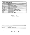
- Fig. 1A is a chart exemplifying an input signal of memory according to the present embodiment
- Fig. 1B is a chart exemplifying an output signal of the memory according thereto
- Fig. 2 is a chart exemplifying an active truth table corresponding to a state of an input signal.
- the memory used in the present embodiment comprises a clock CK, a chip enable CE, a Write enable WE, an input address IA [t-1: 0] (t denotes an address width), input data I [b-1: 0] (b denotes a data width), a partial Write enable BWEB [b/8-1: 0], a low power standby enable SHTDWN, a reset RSTB and an idle enable ZZB as input signals; and comprises output data A [b-1: 0] as an output signal.
- the clock CK is a clock signal used for synchronizing at the time of inputting and outputting data or command to and from the memory.
- the memory inputs and outputs data or a command synchronously with the rise edge of a clock CK in the following description, the memory according to the present embodiment, however, may be configured to input and output data synchronously with the fall edge of a clock CK, or with both the rise and fall edges thereof.
- the chip enable CE is a negative logic signal for receiving a Read/Write instruction at low as shown in Fig. 2.
- the write enable WE is a negative logic signal indicating a Read at high and a Write at low.
- the partial write enable BWEB is for putting mask to a specific bit per byte against a Write when writing to the memory.
- the low power standby enable SHTDWN is a signal for making the memory in a low-power standby mode, putting it in the minimum power consumption mode without retaining data when the signal is high.
- the reset RSTB is a signal for resetting the memory for initialization.
- the idle enable ZZB is a signal for making the memory in an idle (IDL) state at low.
- the present embodiment is configured to put a limitation to timing for receiving a command in order to implement a memory controller allowing a simple description by a hardware description language, that is, having a small circuit size, and enabling an easy validation of a design and of a description content written by the hardware description language.
- a conventional SDRAM received new command any time after two clocks after receiving a command
- the memory according to the present embodiment is configured to receive a command only at every two clocks. Setting such a limitation uniquely determines a supposed pattern, thereby making the circuit configuration simple and enabling an easy validation of a description content written by the hardware description language.
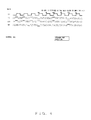
- Fig. 3 shows charts each exemplifying an operation timing of the semiconductor memory according to the present embodiment.
- the drawings show usual Read and Write operations.
- commands are received only at every two clocks, i.e., an Idle command, an RD command, a WT command, et cetera, while no command is received at the timing of one clock between commands.
- commands are received only at every four clocks, i.e., an RD command, a WT command, an Idle command, et cetera, while no command is received at other timings.
- simplification of a clock timing specification for a command reception enables an easy design of a memory controller for controlling the memory, and an easy description of a memory operation specification by a hardware description language, such as Verilog and VHDL, and an easy verification thereof.
- setup value of a BL shall preferably be set to a value of 2 k , such as 2, 4, 8, et cetera. This stems from a k being equal to the number of address signals IA which becomes unnecessary according to a BL setting.
- Fig. 4 is a chart exemplifying an operation timing immediately after an initialization of semiconductor memory according to the present embodiment.
- the memory according to the present embodiment is configured to make the initial WT command following an initialization the basic point for a command reception.
- an RD command or a refresh (Ref) command may be made a basic point for a command reception, in place of the WT command.
- data needs to be first written in order to use the memory and therefore it is desirable to make a WT command the basic point.
- Making the first WT command the basic point enables a provision of a function other than the original function to other commands during the time until an initial WT command is input. This point of view is described later.
- Fig. 4 exemplifies the case of making a WT command initially received after initializing the semiconductor memory the reference, a WT command initially received not only after an initialization but also after turning the power on or during a low-power standby mode can likewise be made a reference for a command reception.
- the configuration is also such that a once set clock constituting a reference is initialized by either of an initialization, a low-power standby and turning a power on.
- the memory according to the present embodiment is configured to have the capability of providing for instance an RD command, which is input prior to being input by an initial WT command constituting a reference, with another function, e.g., the function as command for performing various setups of the memory in the same manner as an MRS command of SDRAM.
- Fig. 5 exemplifies such a case.
- Fig. 5 shows the case of making a WT command a reference, and providing an RD command, which is input prior to being input by an initial WT command, with the function as a command (this command is noted as MRS command in the following description) for setting a value in a register which sets various setup values such as BL and RL for the memory.
- Fig. 5 makes an RD command input prior to an initial WT command an MRS command, and specifies a setup value for a register by an address code which has simultaneously been input.
- the case correlates a setup content with each address code, such as specifying setup values of BL for the address codes A0 and A1 and those of RL for the address codes A2 and A3 for example, in advance, followed by setting these setup values by address codes which are input together with an RD command.
- a setup content such as specifying setup values of BL for the address codes A0 and A1 and those of RL for the address codes A2 and A3 for example, in advance, followed by setting these setup values by address codes which are input together with an RD command.
- This configuration makes it possible to perform various setups for the memory before a data read/write to/from the memory is started.
- MRS command may be not only BL, RL and WL, but also other setups for evaluation, including an internal timing of a device and a voltage level of an internal generation power source for example.
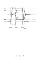
- Fig. 6 is a diagram showing a timing chart at the time of reading data of a typical DRAM.
- the WL indicates a word line (i.e., a line selection line); the BL and "/BL" indicate bit lines,; the VDD indicates a power source voltage level; the GND indicates a ground level; and the V0 and V1 indicate voltage levels of an internal generation.
- Data in a memory cell selected by the word line WL is read as a result of the data being amplified by a sense amplifier SA after a period of T, during which the data is read by the bit line BL and /BL, passes, and then the word line WL is turned off, followed by resetting (i.e., turning off) the sense amplifier SA.
- Voltage levels of the voltages V0 and V1, a rise timing WLon and a fall timing WLoff of the word line WL, and timing SAon/SAoff for setting/resetting the sense amplifier SA are important parameters for designing DRAM.
- the level and timing can be freely changed by an MRS, it is effective for evaluating the produced memory.
- the above described voltage level and/or internal timing are set by an MRS command.
- An example configuration is such that a part of address codes (e.g., addresses A6 and A7), which are input simultaneously with an MRS command, is correlated as a value for setting a voltage level of the V0, followed by selecting a voltage level to be set to the V0 from among the four voltages, i.e., V0 1 , V0 2 , V0 3 and V0 4 , according to a value of the address code.
- the present embodiment is configured to limit so as to carry out various setups for the memory prior to being input by a specific command (e.g., a WT command) after turning a power on or an initialization, and therefore a circuit configuration of a memory controller for controlling the memory is simpler than one for the conventionally configured memory, and a design and a verification thereafter are proportionately easier.
- a specific command e.g., a WT command
- the function according to the mode register set mode is the one mainly used for a device evaluation, et cetera, which sometimes includes a function useless for a memory user.
- it may be configured such that an MRS command normally does not function by way of a metal option, et cetera, in order to prevent the user from erroneously entering a mode register set mode which changes a setup by an MRS command.
- Fig. 7 is for describing an operation of such a case.
- Fig. 7 also exemplifies the case of making a WT command a reference, and providing an RD command, which is input prior to being input by an initial WT command, with the function as an MRS command for setting a value in a register which sets various setup values such as BL and RL for the memory.
- a setup value is not changed by entering a mode register set mode unless four consecutive RD commands are input prior to being input by a WT command constituting a reference.
- the first two among the four RD commands are keys (i.e., a key 1 and a key 2) for examining whether or not a value of an address code at the time of inputting the keys identifies with a predefined specific value, recognizing an RD command input in the third place as an MRS command if the address code identifies with the specific value and not receive the RD command input in the third place as an MRS command if the address code does not identify therewith.
- an RD command in the fourth place following the MRS command in the third place is also a key command (i.e., a key 3) for setting a setup value specified by the MRS command actually to the memory only if an address code of the key 3 identifies with the specific value.
- a key command i.e., a key 3 for setting a setup value specified by the MRS command actually to the memory only if an address code of the key 3 identifies with the specific value.
- the configuration is such that the two keys, i.e., the keys 1 and 2, must be passed for receiving an MRS command in Fig. 7, the number of the keys, however, may be one, or more than two.
- Another configuration may be such that an input of an MRS command in the third place is immediately followed by a setup value being set to a register within memory, in lieu of equipping with a key 3.
- Fig. 7B exemplifies such a case.
- Such a configuration of equipping keys for preventing an erroneous setup enables a prevention of an erroneous setup for the memory.
- Fig. 8 is a diagram exemplifying transitions of operation states of memory according to the present embodiment.
- the Start means turning a power on, and the memory according to the present embodiment transitions to a Write mode (WT) 3 by a command after an initialization mode 1.
- the Write mode 3 is a mode for writing data to the memory. It is possible to freely transition from the Write mode 3 to a Read mode (RD) 4 for reading data, a Refresh mode (Ref) 5 for performing refreshing processing and an Idle (IDLE) 6 for retaining data by the respective commands. It is also possible to transition from the four modes to a low-power standby mode 7 for suppressing a power consumption to a minimum without retaining data, and also therefrom to a Write mode 3. It is further possible to transition from the five modes and initialization mode to a hang-up mode 8 for destructing all memory cell data and not receiving an RD/WT commands, and also therefrom to the initialization mode 1.
- a configuration may be so as to transition from the initialization mode 1 to a mode register set mode 2 for performing various setups for the memory. And it is possible to transition from the mode register set mode 2 to the Write mode 3.
- a specific command constituting a reference (i.e., a WT command), which has been described by referring to Fig. 4, corresponds not only to an initial WT command after an initialization mode but also to an initial WT command after a low-power standby mode as shown in the state transition diagram of Fig. 8.
- Fig. 9 shows block diagrams of the memory according to the present embodiment.
- Memory 11a includes a memory cell array 12 comprising a memory cell and a selection circuit for selecting a memory cell, and comprises a memory control unit 13a for controlling the memory cell array 12, with a memory controller 14a for controlling the above described memory being placed within the memory control unit 13a.
- the memory controller 14a comprises a CMD control 15a for controlling an operation of the memory by a command that is externally received, and a Mode register unit 16a for determining an operation mode by selecting one from a plurality of operation modes.
- the CMD control 15a comprises a CK reception unit 17a for receiving a clock and a CMD reception unit 18a for receiving a command.
- a controller 14b may be configured to externally equipped with a generic use memory 11b comprising a memory array 12 and a memory control unit 13b.
- the controller 14b comprises an interface unit 19 for managing a connection with the generic use memory 11b, in addition to the CMD control 15 and a Mode register unit 16b.
- FIG. 9B another configuration may be so as to place the Mode register unit 16b on the side of the generic use memory 11b.
- the memory controller according to the present embodiment can be implemented as a part of memory, or as a configuration for externally connected to generic use memory such as SDRAM.
- memory according to the present embodiment may be other types of memory provided that they are for inputting and outputting data synchronously with an input clock, such as SRAM, in lieu of being limited to the DRAM.
Landscapes
- Engineering & Computer Science (AREA)
- Microelectronics & Electronic Packaging (AREA)
- Computer Hardware Design (AREA)
- Databases & Information Systems (AREA)
- Dram (AREA)
- Memory System (AREA)
Abstract
Description
- The present invention relates to a technique for controlling semiconductor memory of a synchronous transfer system.
- A burst transfer for raising a transfer speed by partially eliminating procedures such as specifying an address is one of effective means for improving a data transfer rate of semiconductor memory when transferring continuous data synchronously with a clock signal.
- For instance, a patent document 1 (Laid-Open
Japanese Patent Application Publication No. 10-199233 - Synchronous DRAM (SDRAM), i.e., generic DRAM, operates when a BL (Burst Length) as one of setup values used for a burst transfer is equal to or greater than two for example, and a value of the BL can be controlled by a Mode Register Set (MRS) command.
- Since control commands such as the MRS command can be input at a discretionary clock, a user is required to utilize SDRAM with an appropriate attention under various limitations such as timing. For example, the user is required to use it by considering a limitation of intervals when continuously accessing the same bank, that of intervals for being able to input an RD (Read) command from an active command, et cetera.
- Incidentally, for a setup value BL, the present specification defines that the case of inputting and outputting data for the duration of N clocks by one RD (Read)/WT (Write) command is BL=N.
- A memory controller managing a control of memory is required to control SDRAM so as to satisfy various constraint conditions, making its design difficult.
- Meanwhile, if a design is tried by describing such a specification by a hardware description language such as Verilog and VHDL (VHSIC (very high speed integrated circuit) description language), a description content becomes complex due to a cumbersomeness of the control. Because of this, not only the description per se is difficult, but also an identification of the description with a specification is difficult to validate. Therefore, adoption of the specification as a logic mixed memory macro levies great loads on both a macro designer (i.e., a describer of Verilog/VHDL) and a macro user.
- The purpose of the present invention is to provide a memory control technique for enabling easy designs of semiconductor memory and a memory controller for controlling the memory for the semiconductor memory carrying out a synchronous transfer.
- According to the present invention, semiconductor memory, premising the one for inputting and outputting data synchronously with a clock, comprises a clock reception unit and a command reception unit.
- The clock reception unit receives the clock.
- The command reception unit initially receives a first specific command synchronizing with the clock after turning a power on, after a low-power standby or after an initialization, followed by starting a command reception.
- The first specific command is a Write command for example, and simplification of a command reception makes it possible to simplify a configuration of a circuit used for a control.
- An alternative configuration may be such that the command reception unit receives a command at every N clocks with a clock at which the first specific command is initially received being the basic point in time when the semiconductor memory inputs and outputs data for a duration of N clocks corresponding to a Read/Write command synchronizing with the clock.
- As such, the configuration for receiving a command only at every specific clock starting from the basis enables simplification of a circuit control.
- Another alternative configuration may further be such that the command reception unit recognizes a second specific command received prior to initially receiving said first specific command as a command which defines an operation mode setup of the semiconductor memory.
- This configuration makes it possible to separate between a control for defining an operation mode of the semiconductor memory and that for reading/writing data, thereby simplifying a control configuration.
- Another possible alternative configuration is such that the command reception unit receives the second specific command when one or more command constituting a key prior to an input of the second specific command.
- This configuration is capable of preventing an erroneous change of an operation mode setup for the semiconductor memory.
- The present invention includes not only semiconductor memory but also a memory controller connected thereto and a control method therefor, within the scope of the present invention.
- The present invention enables easy designs of semiconductor memory and of a memory controller, and additionally simplification of the related circuit configurations. This in turn enables a design and a validation thereafter to be easy.
-
- Fig. 1A is a chart exemplifying an input signal of memory according to the present embodiment;
- Fig. 1B is a chart exemplifying an output signal of memory according to the present embodiment;
- Fig. 2 is a chart exemplifying an active truth table corresponding to a state of an input signal;
- Fig. 3A and Fig. 3B are charts each exemplifying an operation timing according to the present embodiment;
- Fig. 4 is a chart exemplifying an operation timing immediately after an initialization of semiconductor memory according to the present embodiment;
- Fig. 5 is a chart showing the case of providing a function as MRS command vis-6-vis a command input prior to a command constituting a first reference being input;
- Fig. 6 is a diagram showing a timing chart at the time of reading data of a typical DRAM;
- Fig. 7A and Fig. 7B are diagrams each describing the case of equipping a key for the purpose of entering a mode register set mode;
- Fig. 8 is a diagram exemplifying transitions of operation states of memory according to the present embodiment; and
- Fig. 9A and Fig. 9B are block diagrams of memory according to the present embodiment.
- The following is a description of the preferred embodiment of the present invention by referring to the accompanying drawings.
- Fig. 1A is a chart exemplifying an input signal of memory according to the present embodiment; and Fig. 1B is a chart exemplifying an output signal of the memory according thereto. Fig. 2 is a chart exemplifying an active truth table corresponding to a state of an input signal.
- According to the examples shown by Figs. 1A and 1B, the memory used in the present embodiment comprises a clock CK, a chip enable CE, a Write enable WE, an input address IA [t-1: 0] (t denotes an address width), input data I [b-1: 0] (b denotes a data width), a partial Write enable BWEB [b/8-1: 0], a low power standby enable SHTDWN, a reset RSTB and an idle enable ZZB as input signals; and comprises output data A [b-1: 0] as an output signal.
- Among these, the clock CK is a clock signal used for synchronizing at the time of inputting and outputting data or command to and from the memory. Note that the memory inputs and outputs data or a command synchronously with the rise edge of a clock CK in the following description, the memory according to the present embodiment, however, may be configured to input and output data synchronously with the fall edge of a clock CK, or with both the rise and fall edges thereof.
- The chip enable CE is a negative logic signal for receiving a Read/Write instruction at low as shown in Fig. 2. The write enable WE is a negative logic signal indicating a Read at high and a Write at low.
- The partial write enable BWEB is for putting mask to a specific bit per byte against a Write when writing to the memory. The low power standby enable SHTDWN is a signal for making the memory in a low-power standby mode, putting it in the minimum power consumption mode without retaining data when the signal is high. The reset RSTB is a signal for resetting the memory for initialization. The idle enable ZZB is a signal for making the memory in an idle (IDL) state at low.
- The next description is of an outline of a memory control according to the present embodiment.
- The present embodiment is configured to put a limitation to timing for receiving a command in order to implement a memory controller allowing a simple description by a hardware description language, that is, having a small circuit size, and enabling an easy validation of a design and of a description content written by the hardware description language.
- For instance, for the BL being equal to 2 (two), a conventional SDRAM received new command any time after two clocks after receiving a command, whereas the memory according to the present embodiment is configured to receive a command only at every two clocks. Setting such a limitation uniquely determines a supposed pattern, thereby making the circuit configuration simple and enabling an easy validation of a description content written by the hardware description language.
- Fig. 3 shows charts each exemplifying an operation timing of the semiconductor memory according to the present embodiment. The drawings show usual Read and Write operations.
- Note that Fig. 3 exemplifies the case of Read Latency (RL)= 1, and Write Latency (WL)= 0. When RL= 1, Read data is output so as to enable data to be imported at the timing of the next clock following a provision of an RD (Read) command, and when WL= 0, Write data is input at the timing of the same clock as a WT (Write) command.
- Fig. 3A shows the case of BL= 2, where the memory according to the present embodiment is configured to receive an RD and a WT commands at every two clocks. Likewise, in the case of BL= 4 shown by Fig. 3B, the memory receives a command at every four clocks. And the memory is configured to not receive a command at other clock timings except for a low power standby command and an initialization command.
- In Fig. 3A for example, commands are received only at every two clocks, i.e., an Idle command, an RD command, a WT command, et cetera, while no command is received at the timing of one clock between commands. Likewise in Fig. 3B, commands are received only at every four clocks, i.e., an RD command, a WT command, an Idle command, et cetera, while no command is received at other timings.
- As such, simplification of a clock timing specification for a command reception enables an easy design of a memory controller for controlling the memory, and an easy description of a memory operation specification by a hardware description language, such as Verilog and VHDL, and an easy verification thereof.
- Note that the setup value of a BL shall preferably be set to a value of 2k, such as 2, 4, 8, et cetera. This stems from a k being equal to the number of address signals IA which becomes unnecessary according to a BL setting.
- Incidentally in Fig. 3, as a BWEB signal is input at the time of a WT command execution, the data written is masked, and therefore the data writing is not carried out. In Fig. 3A for example, the data D0 is not written to a memory cell, while in Fig. 3B, the data D1 is not written to a memory cell.
- Fig. 4 is a chart exemplifying an operation timing immediately after an initialization of semiconductor memory according to the present embodiment.
- When BL= 2 for example, commands are received at every two clocks as described above, the basic point in time needs to be clarified. The memory according to the present embodiment is configured to make the initial WT command following an initialization the basic point for a command reception.
- Incidentally, an RD command or a refresh (Ref) command may be made a basic point for a command reception, in place of the WT command. However, data needs to be first written in order to use the memory and therefore it is desirable to make a WT command the basic point. Making the first WT command the basic point enables a provision of a function other than the original function to other commands during the time until an initial WT command is input. This point of view is described later.
- In the example shown by Fig. 4, an RD command and Ref command are ignored until an initial WT command is input after initializing the memory, and therefore an idle state is maintained.
- Then, as an initial WT command is input to the memory, a command is received at every two clocks if BL= 2, or every four clocks if BL= 4, sequentially, from the basic point at which the aforementioned WT command has been received.
- Fig. 4 exemplifies the case of BL= 2, where the initial WT command is input, followed by the Ref command, RD command, et cetera, being sequentially received at every two clocks with the clock at which the aforementioned WT command has been received being the reference, while no command is received at timings of one clock between commands.
- Note that Fig. 4 exemplifies the case of making a WT command initially received after initializing the semiconductor memory the reference, a WT command initially received not only after an initialization but also after turning the power on or during a low-power standby mode can likewise be made a reference for a command reception.
- The configuration is also such that a once set clock constituting a reference is initialized by either of an initialization, a low-power standby and turning a power on.
- The next description is of the case of providing a command with a function other than the original function when another command is input prior to being input by a specific command (e.g., a WT command), shown in Fig. 4, which constitutes a reference.
- The memory according to the present embodiment is configured to have the capability of providing for instance an RD command, which is input prior to being input by an initial WT command constituting a reference, with another function, e.g., the function as command for performing various setups of the memory in the same manner as an MRS command of SDRAM.
- In this case, if an RD command is input prior to being input by an initial WT command, it is possible to carry out not only a setup of a value of BL, RL and WL but also a change of an internal operation timing, an adjustment of an internal generation voltage, et cetera, for evaluation, from an address code that is simultaneously input.
- Fig. 5 exemplifies such a case.
- Fig. 5 shows the case of making a WT command a reference, and providing an RD command, which is input prior to being input by an initial WT command, with the function as a command (this command is noted as MRS command in the following description) for setting a value in a register which sets various setup values such as BL and RL for the memory.
- The case of Fig. 5 makes an RD command input prior to an initial WT command an MRS command, and specifies a setup value for a register by an address code which has simultaneously been input.
- For example, the case correlates a setup content with each address code, such as specifying setup values of BL for the address codes A0 and A1 and those of RL for the address codes A2 and A3 for example, in advance, followed by setting these setup values by address codes which are input together with an RD command.
- This configuration makes it possible to perform various setups for the memory before a data read/write to/from the memory is started.
- And what are possible to set by the MRS command may be not only BL, RL and WL, but also other setups for evaluation, including an internal timing of a device and a voltage level of an internal generation power source for example.
- Fig. 6 is a diagram showing a timing chart at the time of reading data of a typical DRAM.
- Referring to Fig. 6, the WL indicates a word line (i.e., a line selection line); the BL and "/BL" indicate bit lines,; the VDD indicates a power source voltage level; the GND indicates a ground level; and the V0 and V1 indicate voltage levels of an internal generation.
- Data in a memory cell selected by the word line WL is read as a result of the data being amplified by a sense amplifier SA after a period of T, during which the data is read by the bit line BL and /BL, passes, and then the word line WL is turned off, followed by resetting (i.e., turning off) the sense amplifier SA.
- Voltage levels of the voltages V0 and V1, a rise timing WLon and a fall timing WLoff of the word line WL, and timing SAon/SAoff for setting/resetting the sense amplifier SA are important parameters for designing DRAM.
- If the level and timing can be freely changed by an MRS, it is effective for evaluating the produced memory.
- As a method for the setting, the above described voltage level and/or internal timing are set by an MRS command. An example configuration is such that a part of address codes (e.g., addresses A6 and A7), which are input simultaneously with an MRS command, is correlated as a value for setting a voltage level of the V0, followed by selecting a voltage level to be set to the V0 from among the four voltages, i.e., V01, V02, V03 and V04, according to a value of the address code.
- It is possible to obtain information such as a design margin relating to a device by comparing evaluation results obtained by changing these voltage levels and internal timings.
- As described above, the present embodiment is configured to limit so as to carry out various setups for the memory prior to being input by a specific command (e.g., a WT command) after turning a power on or an initialization, and therefore a circuit configuration of a memory controller for controlling the memory is simpler than one for the conventionally configured memory, and a design and a verification thereafter are proportionately easier.
- Note that the function according to the mode register set mode is the one mainly used for a device evaluation, et cetera, which sometimes includes a function useless for a memory user. In such a case, it may be configured such that an MRS command normally does not function by way of a metal option, et cetera, in order to prevent the user from erroneously entering a mode register set mode which changes a setup by an MRS command.
- It is also possible to equip a key for entering the mode register set mode in order to inhibit an erroneous use of the aforementioned mode.
- Fig. 7 is for describing an operation of such a case.
- Fig. 7 also exemplifies the case of making a WT command a reference, and providing an RD command, which is input prior to being input by an initial WT command, with the function as an MRS command for setting a value in a register which sets various setup values such as BL and RL for the memory.
- In the case exemplified by Fig. 7A, a setup value is not changed by entering a mode register set mode unless four consecutive RD commands are input prior to being input by a WT command constituting a reference. And the first two among the four RD commands are keys (i.e., a
key 1 and a key 2) for examining whether or not a value of an address code at the time of inputting the keys identifies with a predefined specific value, recognizing an RD command input in the third place as an MRS command if the address code identifies with the specific value and not receive the RD command input in the third place as an MRS command if the address code does not identify therewith. - And an RD command in the fourth place following the MRS command in the third place is also a key command (i.e., a key 3) for setting a setup value specified by the MRS command actually to the memory only if an address code of the
key 3 identifies with the specific value. - Incidentally, the configuration is such that the two keys, i.e., the
keys - Another configuration may be such that an input of an MRS command in the third place is immediately followed by a setup value being set to a register within memory, in lieu of equipping with a
key 3. - Fig. 7B exemplifies such a case.
- In the case of Fig. 7B, if an address code identifies with a specific value in the
keys - Such a configuration of equipping keys for preventing an erroneous setup enables a prevention of an erroneous setup for the memory.
- Fig. 8 is a diagram exemplifying transitions of operation states of memory according to the present embodiment.
- Referring to Fig. 8, the Start means turning a power on, and the memory according to the present embodiment transitions to a Write mode (WT) 3 by a command after an
initialization mode 1. TheWrite mode 3 is a mode for writing data to the memory. It is possible to freely transition from theWrite mode 3 to a Read mode (RD) 4 for reading data, a Refresh mode (Ref) 5 for performing refreshing processing and an Idle (IDLE) 6 for retaining data by the respective commands. It is also possible to transition from the four modes to a low-power standby mode 7 for suppressing a power consumption to a minimum without retaining data, and also therefrom to aWrite mode 3. It is further possible to transition from the five modes and initialization mode to a hang-upmode 8 for destructing all memory cell data and not receiving an RD/WT commands, and also therefrom to theinitialization mode 1. - A configuration may be so as to transition from the
initialization mode 1 to a mode register setmode 2 for performing various setups for the memory. And it is possible to transition from the mode register setmode 2 to theWrite mode 3. - Note that inputs of signals to the SHTDWN and RSTB terminals shown in Fig. 1 transition to the
initialization mode 1 and low-power standby mode 7. These signals are asynchronous signals which do not synchronize with a clock CK. - Meanwhile, a specific command constituting a reference (i.e., a WT command), which has been described by referring to Fig. 4, corresponds not only to an initial WT command after an initialization mode but also to an initial WT command after a low-power standby mode as shown in the state transition diagram of Fig. 8.
- Fig. 9 shows block diagrams of the memory according to the present embodiment.
-
Memory 11a according to the present embodiment includes amemory cell array 12 comprising a memory cell and a selection circuit for selecting a memory cell, and comprises amemory control unit 13a for controlling thememory cell array 12, with amemory controller 14a for controlling the above described memory being placed within thememory control unit 13a. Thememory controller 14a comprises aCMD control 15a for controlling an operation of the memory by a command that is externally received, and aMode register unit 16a for determining an operation mode by selecting one from a plurality of operation modes. TheCMD control 15a comprises aCK reception unit 17a for receiving a clock and aCMD reception unit 18a for receiving a command. - Also as shown by Fig. 9B, a
controller 14b according to the present embodiment may be configured to externally equipped with ageneric use memory 11b comprising amemory array 12 and amemory control unit 13b. In such a case, thecontroller 14b comprises aninterface unit 19 for managing a connection with thegeneric use memory 11b, in addition to the CMD control 15 and aMode register unit 16b. - In the configuration shown by Fig. 9B, another configuration may be so as to place the
Mode register unit 16b on the side of thegeneric use memory 11b. - As described above, the memory controller according to the present embodiment can be implemented as a part of memory, or as a configuration for externally connected to generic use memory such as SDRAM.
- Note that the above description is provided by limiting memory according to the present embodiment to DRAM, the memory according thereto may be other types of memory provided that they are for inputting and outputting data synchronously with an input clock, such as SRAM, in lieu of being limited to the DRAM.
Claims (20)
- Semiconductor memory for inputting and outputting data synchronously with a clock, comprising:a clock reception unit (17a,17b) for receiving the clock; anda command reception unit (18a,18b) for initially receiving a first specific command synchronizing with the clock after turning a power on, after a low-power standby or after an initialization, followed by starting a command reception.
- The semiconductor memory according to claim 1, wherein
said first specific command is a Write command. - The semiconductor memory according to claim 1, wherein
said command reception unit (18a,18b) invalidates a command which is received prior to initially receiving said first specific command synchronizing with said clock. - The semiconductor memory according to claim 1, wherein
said command reception unit (18a,18b) receives a command at every N clocks with a clock at which said first specific command is initially received being the basic point in time when the semiconductor memory inputs and outputs data for a duration of N clocks corresponding to a Read/Write command synchronizing with the clock. - The semiconductor memory according to claim 4, wherein
said N is equal to 2k, where k is an integer being equal to or greater than 1 (one). - The semiconductor memory according to claim 4, wherein
a clock constituting said basic point is initialized at either of an initialization, a low-power standby and turning a power on. - The semiconductor memory according to claim 1, wherein
said command reception unit (18a,18b) recognizes a second specific command received prior to initially receiving said first specific command as a command which defines an operation mode setup of the semiconductor memory. - The semiconductor memory according to claim 7, wherein
said operation mode setup includes a setup of Burst Latency (BL). - The semiconductor memory according to claim 7, wherein
said operation mode setup includes a setup of Read Latency (RL). - The semiconductor memory according to claim 7, wherein
said operation mode setup includes a setup of Write Latency (WL). - The semiconductor memory according to claim 7, wherein
said operation mode setup includes a setup of an internal timing or an internal voltage level of the semiconductor memory. - The semiconductor memory according to claim 7, wherein
said second specific command is a Read command. - The semiconductor memory according to claim 7, wherein
said command reception unit receives said second specific command when one or more command constituting a key prior to an input of the second specific command. - The semiconductor memory according to claim 13, wherein
said command reception unit receives said second specific command when an address code which is input together with a command constituting said key identifies with a specific value, - The memory according to claim 7, wherein
an operation mode setup for the semiconductor memory by said second specific command is validated when a command constituting a key is input after inputting the second specific command. - The semiconductor memory according to claim 7, wherein
an operation mode setup for the semiconductor memory by said second specific command is validated at the time of inputting the aforementioned second specific command. - The semiconductor memory according to claim 7, further comprising
a mode register (16a, 16b) for setting an operation mode of the semiconductor memory, wherein an operation mode setup for the semiconductor memory by said second specific command is set in the mode register. - A memory controller connected to semiconductor memory for inputting and outputting data synchronously with a clock, comprising:a clock reception unit (17b) for receiving the clock; anda command reception unit (18b) for initially receiving a first specific command synchronizing with the clock after turning a power on, after a low-power standby or after an initialization, followed by starting a command reception.
- The memory controller according to claim 18, wherein
said command reception unit receives a command at every N clocks with a clock at which said first specific command is initially received being the basic point in time when the semiconductor memory inputs and outputs data for a duration of N clocks corresponding to a Read/Write command synchronizing with the clock. - A control method used for semiconductor memory for inputting and outputting data synchronously with a clock, comprising the steps of
receiving the clock; and
initially receiving a first specific command synchronizing with the clock after turning a power on, after a low-power standby or after an initialization, followed by starting a command reception.
Applications Claiming Priority (1)
| Application Number | Priority Date | Filing Date | Title |
|---|---|---|---|
| JP2006020427A JP2007200504A (en) | 2006-01-30 | 2006-01-30 | Semiconductor memory, memory controller, and semiconductor memory control method |
Publications (2)
| Publication Number | Publication Date |
|---|---|
| EP1814119A1 true EP1814119A1 (en) | 2007-08-01 |
| EP1814119B1 EP1814119B1 (en) | 2010-03-17 |
Family
ID=37890950
Family Applications (1)
| Application Number | Title | Priority Date | Filing Date |
|---|---|---|---|
| EP06114687A Not-in-force EP1814119B1 (en) | 2006-01-30 | 2006-05-30 | Semiconductor memory, memory controller and control method for semiconductor memory |
Country Status (7)
| Country | Link |
|---|---|
| US (1) | US7599244B2 (en) |
| EP (1) | EP1814119B1 (en) |
| JP (1) | JP2007200504A (en) |
| KR (1) | KR100787084B1 (en) |
| CN (1) | CN100594552C (en) |
| DE (1) | DE602006012928D1 (en) |
| TW (1) | TWI317519B (en) |
Families Citing this family (8)
| Publication number | Priority date | Publication date | Assignee | Title |
|---|---|---|---|---|
| JP4896450B2 (en) * | 2005-06-30 | 2012-03-14 | 株式会社東芝 | Storage device |
| JP4778321B2 (en) * | 2006-01-30 | 2011-09-21 | 富士通セミコンダクター株式会社 | Semiconductor memory, memory system |
| KR101609250B1 (en) * | 2008-11-26 | 2016-04-06 | 삼성전자주식회사 | Interface method for transmitting and receiving system using data stream |
| KR101096268B1 (en) | 2010-04-01 | 2011-12-22 | 주식회사 하이닉스반도체 | Command decoder and semiconductor memory device |
| TWI594251B (en) * | 2012-06-06 | 2017-08-01 | 慧榮科技股份有限公司 | Memory control method, controller and electronic device |
| CN103473146B (en) | 2012-06-06 | 2017-04-19 | 慧荣科技股份有限公司 | Memory control method, memory controller and electronic device |
| TWI508066B (en) * | 2013-04-30 | 2015-11-11 | Mstar Semiconductor Inc | Memory controller and signal generation method thereof |
| EP3706685A4 (en) * | 2017-11-07 | 2021-08-11 | 3M Innovative Properties Company | REPLACEABLE SOUND ATTENUATION DEVICE DETECTION |
Citations (2)
| Publication number | Priority date | Publication date | Assignee | Title |
|---|---|---|---|---|
| WO2000020954A1 (en) * | 1998-10-06 | 2000-04-13 | Intel Corporation | A self-synchronizing method and apparatus for exiting dynamic random access memory from a low power state |
| US20030126356A1 (en) * | 1997-08-11 | 2003-07-03 | Advanced Memory International, Inc. | Memory system having synchronous-link DRAM (SLDRAM) devices and controller |
Family Cites Families (22)
| Publication number | Priority date | Publication date | Assignee | Title |
|---|---|---|---|---|
| JP2813223B2 (en) * | 1990-01-22 | 1998-10-22 | 富士通株式会社 | Semiconductor storage device |
| KR100245078B1 (en) | 1996-11-15 | 2000-02-15 | 김영환 | High-speed burst control method and apparatus |
| JPH10233091A (en) * | 1997-02-21 | 1998-09-02 | Hitachi Ltd | Semiconductor storage device and data processing device |
| JP4141520B2 (en) | 1997-11-14 | 2008-08-27 | 株式会社ルネサステクノロジ | Synchronous semiconductor memory device |
| JP2000030442A (en) * | 1998-07-10 | 2000-01-28 | Mitsubishi Electric Corp | Synchronous semiconductor memory device |
| JP4043151B2 (en) * | 1998-08-26 | 2008-02-06 | 富士通株式会社 | High speed random accessible memory device |
| JP4156721B2 (en) * | 1998-09-18 | 2008-09-24 | 富士通株式会社 | Semiconductor integrated circuit device |
| US6222785B1 (en) * | 1999-01-20 | 2001-04-24 | Monolithic System Technology, Inc. | Method and apparatus for refreshing a semiconductor memory using idle memory cycles |
| KR100304705B1 (en) * | 1999-03-03 | 2001-10-29 | 윤종용 | SDRAM having posted CAS latency and CAS latency control method therefor |
| JP4864187B2 (en) * | 2000-01-19 | 2012-02-01 | 富士通セミコンダクター株式会社 | Semiconductor integrated circuit |
| JP4201490B2 (en) * | 2000-04-28 | 2008-12-24 | 富士通マイクロエレクトロニクス株式会社 | Memory circuit having automatic precharge function and integrated circuit device having automatic internal command function |
| JP4569915B2 (en) * | 2000-08-11 | 2010-10-27 | エルピーダメモリ株式会社 | Semiconductor memory device |
| JP4216457B2 (en) * | 2000-11-30 | 2009-01-28 | 富士通マイクロエレクトロニクス株式会社 | Semiconductor memory device and semiconductor device |
| JP3737437B2 (en) * | 2001-02-01 | 2006-01-18 | Necエレクトロニクス株式会社 | Semiconductor memory and entry method of operation mode thereof |
| JP4707255B2 (en) * | 2001-04-26 | 2011-06-22 | ルネサスエレクトロニクス株式会社 | Semiconductor memory device |
| DE10232859B4 (en) * | 2001-07-18 | 2014-11-13 | Samsung Electronics Co., Ltd. | Method for generating an initialization signal |
| JP4000028B2 (en) | 2001-09-18 | 2007-10-31 | 株式会社東芝 | Synchronous semiconductor memory device |
| JP4570321B2 (en) * | 2002-10-29 | 2010-10-27 | ルネサスエレクトロニクス株式会社 | Semiconductor memory device |
| JP4327482B2 (en) * | 2003-03-18 | 2009-09-09 | 富士通マイクロエレクトロニクス株式会社 | Synchronous semiconductor memory device |
| JP4152308B2 (en) * | 2003-12-08 | 2008-09-17 | エルピーダメモリ株式会社 | Semiconductor integrated circuit device |
| JP4827399B2 (en) * | 2004-05-26 | 2011-11-30 | ルネサスエレクトロニクス株式会社 | Semiconductor memory device |
| US7900099B2 (en) * | 2005-01-25 | 2011-03-01 | Micron Technology, Inc. | Enabling test modes of individual integrated circuit devices out of a plurality of integrated circuit devices |
-
2006
- 2006-01-30 JP JP2006020427A patent/JP2007200504A/en active Pending
- 2006-05-18 TW TW095117627A patent/TWI317519B/en not_active IP Right Cessation
- 2006-05-22 US US11/437,719 patent/US7599244B2/en active Active
- 2006-05-23 KR KR1020060045938A patent/KR100787084B1/en not_active Expired - Fee Related
- 2006-05-30 DE DE602006012928T patent/DE602006012928D1/en active Active
- 2006-05-30 EP EP06114687A patent/EP1814119B1/en not_active Not-in-force
- 2006-06-12 CN CN200610087024A patent/CN100594552C/en not_active Expired - Fee Related
Patent Citations (2)
| Publication number | Priority date | Publication date | Assignee | Title |
|---|---|---|---|---|
| US20030126356A1 (en) * | 1997-08-11 | 2003-07-03 | Advanced Memory International, Inc. | Memory system having synchronous-link DRAM (SLDRAM) devices and controller |
| WO2000020954A1 (en) * | 1998-10-06 | 2000-04-13 | Intel Corporation | A self-synchronizing method and apparatus for exiting dynamic random access memory from a low power state |
Also Published As
| Publication number | Publication date |
|---|---|
| US7599244B2 (en) | 2009-10-06 |
| KR100787084B1 (en) | 2007-12-21 |
| TW200729205A (en) | 2007-08-01 |
| US20070177449A1 (en) | 2007-08-02 |
| KR20070078772A (en) | 2007-08-02 |
| TWI317519B (en) | 2009-11-21 |
| CN100594552C (en) | 2010-03-17 |
| EP1814119B1 (en) | 2010-03-17 |
| CN101013596A (en) | 2007-08-08 |
| JP2007200504A (en) | 2007-08-09 |
| DE602006012928D1 (en) | 2010-04-29 |
Similar Documents
| Publication | Publication Date | Title |
|---|---|---|
| JP4932856B2 (en) | Apparatus and method for adjusting operating parameters of an integrated circuit | |
| USRE41245E1 (en) | Semiconductor memory device | |
| JP5144882B2 (en) | Semiconductor memory device | |
| JP4663274B2 (en) | MEMORY CONTROLLER, SMART CARD HAVING THE SAME, AND MEMORY DATA READING OPERATION CONTROL METHOD | |
| JP2011040041A (en) | Control method of memory device for performing write leveling operation, write leveling method of memory device, memory controller performing write leveling operation, memory device and memory system | |
| KR100922412B1 (en) | Semiconductor memory and method for controlling the same | |
| US7610455B2 (en) | Technique to read special mode register | |
| JP2008305350A (en) | Memory system, memory device, and method for controlling memory device | |
| EP1858022A2 (en) | Semiconductor memory and operating method of same | |
| US7242631B2 (en) | Semiconductor memory device and information processing system | |
| US7599244B2 (en) | Semiconductor memory, memory controller and control method for semiconductor memory | |
| US20100030954A1 (en) | Information processing system and semiconductor storage device | |
| KR20050034402A (en) | Semiconductor memory device capable of controlling burst length without resetting mode of operation and memory system including the same | |
| US6826114B2 (en) | Data path reset circuit using clock enable signal, reset method, and semiconductor memory device including the data path reset circuit and adopting the reset method | |
| CN100456387C (en) | semiconductor memory | |
| KR100527552B1 (en) | Semi-conductor memory device | |
| US20080247261A1 (en) | Semiconductor memory device and control method thereof | |
| JP4768221B2 (en) | Memory device | |
| KR100408719B1 (en) | tRAS delay control device using clock | |
| JP4568522B2 (en) | Semiconductor memory device | |
| US20030063506A1 (en) | Integrated memory device, method of operating an integrated memory, and memory system having a plurality of integrated memories | |
| JP2005071448A (en) | Semiconductor memory device | |
| KR20030062070A (en) | Apparatus and method for controlling an access of a flash memory | |
| KR20050048120A (en) | Data output circuit of semiconductor memory device |
Legal Events
| Date | Code | Title | Description |
|---|---|---|---|
| PUAI | Public reference made under article 153(3) epc to a published international application that has entered the european phase |
Free format text: ORIGINAL CODE: 0009012 |
|
| AK | Designated contracting states |
Kind code of ref document: A1 Designated state(s): AT BE BG CH CY CZ DE DK EE ES FI FR GB GR HU IE IS IT LI LT LU LV MC NL PL PT RO SE SI SK TR |
|
| AX | Request for extension of the european patent |
Extension state: AL BA HR MK YU |
|
| 17P | Request for examination filed |
Effective date: 20071008 |
|
| 17Q | First examination report despatched |
Effective date: 20080212 |
|
| AKX | Designation fees paid |
Designated state(s): DE FR IT |
|
| RAP1 | Party data changed (applicant data changed or rights of an application transferred) |
Owner name: FUJITSU MICROELECTRONICS LIMITED |
|
| GRAP | Despatch of communication of intention to grant a patent |
Free format text: ORIGINAL CODE: EPIDOSNIGR1 |
|
| RIN1 | Information on inventor provided before grant (corrected) |
Inventor name: SERIZAWA, YUJI Inventor name: ETO, SATOSHI Inventor name: MIYO, TOSHIYA Inventor name: KAWABATA, KUNINORI |
|
| GRAS | Grant fee paid |
Free format text: ORIGINAL CODE: EPIDOSNIGR3 |
|
| GRAA | (expected) grant |
Free format text: ORIGINAL CODE: 0009210 |
|
| AK | Designated contracting states |
Kind code of ref document: B1 Designated state(s): DE FR IT |
|
| REF | Corresponds to: |
Ref document number: 602006012928 Country of ref document: DE Date of ref document: 20100429 Kind code of ref document: P |
|
| PLBE | No opposition filed within time limit |
Free format text: ORIGINAL CODE: 0009261 |
|
| STAA | Information on the status of an ep patent application or granted ep patent |
Free format text: STATUS: NO OPPOSITION FILED WITHIN TIME LIMIT |
|
| REG | Reference to a national code |
Ref country code: FR Ref legal event code: ST Effective date: 20110131 |
|
| 26N | No opposition filed |
Effective date: 20101220 |
|
| PG25 | Lapsed in a contracting state [announced via postgrant information from national office to epo] |
Ref country code: IT Free format text: LAPSE BECAUSE OF FAILURE TO SUBMIT A TRANSLATION OF THE DESCRIPTION OR TO PAY THE FEE WITHIN THE PRESCRIBED TIME-LIMIT Effective date: 20100317 |
|
| PG25 | Lapsed in a contracting state [announced via postgrant information from national office to epo] |
Ref country code: FR Free format text: LAPSE BECAUSE OF NON-PAYMENT OF DUE FEES Effective date: 20100531 |
|
| REG | Reference to a national code |
Ref country code: DE Ref legal event code: R082 Ref document number: 602006012928 Country of ref document: DE Representative=s name: REICHERT & LINDNER PARTNERSCHAFT PATENTANWAELT, DE |
|
| REG | Reference to a national code |
Ref country code: DE Ref legal event code: R082 Ref document number: 602006012928 Country of ref document: DE Representative=s name: REICHERT & LINDNER PARTNERSCHAFT PATENTANWAELT, DE Effective date: 20150512 Ref country code: DE Ref legal event code: R081 Ref document number: 602006012928 Country of ref document: DE Owner name: SOCIONEXT INC., YOKOHAMA-SHI, JP Free format text: FORMER OWNER: FUJITSU SEMICONDUCTOR LTD., YOKOHAMA, KANAGAWA, JP Effective date: 20150512 |
|
| PGFP | Annual fee paid to national office [announced via postgrant information from national office to epo] |
Ref country code: DE Payment date: 20210520 Year of fee payment: 16 |
|
| REG | Reference to a national code |
Ref country code: DE Ref legal event code: R119 Ref document number: 602006012928 Country of ref document: DE |
|
| PG25 | Lapsed in a contracting state [announced via postgrant information from national office to epo] |
Ref country code: DE Free format text: LAPSE BECAUSE OF NON-PAYMENT OF DUE FEES Effective date: 20221201 |