JP4768221B2 - Memory device - Google Patents
Memory device Download PDFInfo
- Publication number
- JP4768221B2 JP4768221B2 JP2003378326A JP2003378326A JP4768221B2 JP 4768221 B2 JP4768221 B2 JP 4768221B2 JP 2003378326 A JP2003378326 A JP 2003378326A JP 2003378326 A JP2003378326 A JP 2003378326A JP 4768221 B2 JP4768221 B2 JP 4768221B2
- Authority
- JP
- Japan
- Prior art keywords
- data
- signal
- mask
- buffer
- gate
- Prior art date
- Legal status (The legal status is an assumption and is not a legal conclusion. Google has not performed a legal analysis and makes no representation as to the accuracy of the status listed.)
- Expired - Fee Related
Links
Images


Classifications
-
- G—PHYSICS
- G11—INFORMATION STORAGE
- G11C—STATIC STORES
- G11C7/00—Arrangements for writing information into, or reading information out from, a digital store
- G11C7/10—Input/output [I/O] data interface arrangements, e.g. I/O data control circuits, I/O data buffers
- G11C7/1078—Data input circuits, e.g. write amplifiers, data input buffers, data input registers, data input level conversion circuits
- G11C7/1087—Data input latches
-
- G—PHYSICS
- G11—INFORMATION STORAGE
- G11C—STATIC STORES
- G11C7/00—Arrangements for writing information into, or reading information out from, a digital store
- G11C7/10—Input/output [I/O] data interface arrangements, e.g. I/O data control circuits, I/O data buffers
- G11C7/1006—Data managing, e.g. manipulating data before writing or reading out, data bus switches or control circuits therefor
-
- G—PHYSICS
- G11—INFORMATION STORAGE
- G11C—STATIC STORES
- G11C7/00—Arrangements for writing information into, or reading information out from, a digital store
- G11C7/10—Input/output [I/O] data interface arrangements, e.g. I/O data control circuits, I/O data buffers
- G11C7/1078—Data input circuits, e.g. write amplifiers, data input buffers, data input registers, data input level conversion circuits
- G11C7/1093—Input synchronization
Description
本発明は、メモリ装置に関し、特にライトイネーブル信号及びデータマスク信号に応じてメモリセルにデータをライトするメモリ装置に関する。 The present invention relates to a memory device, and more particularly to a memory device that writes data to a memory cell in response to a write enable signal and a data mask signal.
メモリ装置には、ライトイネーブル信号及びデータマスク信号に応じてメモリセルにデータをライトするものがある。ライトイネーブル信号及びデータマスク信号に応じて、現サイクルでデータをバッファに取り込み、次サイクルでそのデータを転送してライトする。 Some memory devices write data to memory cells in response to a write enable signal and a data mask signal. In response to the write enable signal and the data mask signal, data is taken into the buffer in the current cycle, and the data is transferred and written in the next cycle.
そのようなメモリ装置では、ライトの誤動作によるデータ誤書き込みを防止する必要がある。また、ライト動作の遅延を防止する必要がある。 In such a memory device, it is necessary to prevent erroneous data writing due to a write malfunction. In addition, it is necessary to prevent a delay in the write operation.
半導体記憶装置でライト動作をするかしないかというぎりぎりの状態で外部からのライト指示があった場合、(1)ライト動作をしない、(2)ライト動作を行い、データやマスク状態を正しく取り込む、のいずれかである必要がある。ライト動作を行う場合に遷移中の意図しないマスク情報を取り込んだり、データを取り込んでないのに前のデータを使って別のアドレスに書き込んでしまったりという誤書き込みは避けなければならない。ただライトコマンドを発生しにくくするという手段ではライト動作が遅くなり、ライトサイクルも遅くなる。 When there is a write instruction from the outside in the state of whether or not to perform the write operation in the semiconductor memory device, (1) the write operation is not performed, (2) the write operation is performed, and the data and the mask state are correctly captured. Must be one of the following. When performing a write operation, it is necessary to avoid erroneous writing such as taking in unintended mask information during transition, or writing to another address using previous data even though data is not taken in. However, the means for making it difficult to generate a write command slows down the write operation and slows down the write cycle.
本発明の目的は、ライト動作を遅らせることなくデータ破壊を防止することができるメモリ装置を提供することである。 An object of the present invention is to provide a memory device that can prevent data destruction without delaying a write operation.
本発明の一観点によれば、ゲート制御により入力されるデータを第1のバッファにバッファリングするためのデータ取り込みゲートと、ゲート制御により前記第1のバッファのデータを入力して第2のバッファにバッファリングするためのデータ転送ゲートと、ゲート制御により前記第2のバッファのデータをデータバスに出力するためのデータライトゲートと、前記データバス上のデータをライトして記憶するためのメモリセルと、データマスク信号によりマスクされると前記データバスを前記メモリセルに接続せず、データマスク信号によりマスク解除されると前記データバスを前記メモリセルに接続するためのセレクタと、ライトイネーブル信号及びデータマスク信号に応じて、第1のサイクルで前記データ取り込みゲートを制御して前記第1のバッファにデータを入力し、前記第1のサイクルの次サイクルで前記データ転送ゲートを制御して前記第1のバッファのデータを前記第2のバッファに入力し前記データライトゲートを制御して前記第2のバッファのデータを前記データバスに出力する制御回路とを有し、前記制御回路は、前記ライトイネーブル信号が活性化してから前記データマスク信号がマスクを指定する状態に変化するまでの間の時間が第1の時間である第1動作モードの場合には、第1のサイクルにおいて、前記データ取り込みゲートの制御により前記第1のバッファにデータを入力せず、かつ前記データ転送ゲートの制御により前記第2のバッファにデータを入力し、かつ前記データライトゲートの制御により前記第2のバッファのデータを前記データバスに出力せず、前記第1のサイクルの次のサイクルにおいて、前記データライトゲートの制御により前記第2のバッファのデータを前記データバスに出力し、前記ライトイネーブル信号が活性化してから前記データマスク信号がマスクを指定する状態に変化するまでの間の時間が前記第1の時間よりも長い第2動作モードの場合には、第1のサイクルにおいて、前記データ取り込みゲートの制御により前記第1のバッファにデータを入力せず、かつ前記データ転送ゲートの制御により前記第2のバッファにデータを入力し、かつ前記データライトゲートの制御により前記第2のバッファのデータを前記データバスに出力し、前記第1のサイクルの次のサイクルにおいて、前記セレクタが前記データバスを前記メモリセルに接続しないようにするメモリ装置が提供される。 According to one aspect of the present invention, a data fetch gate for buffering data input by gate control in a first buffer, and a second buffer by inputting data of the first buffer by gate control A data transfer gate for buffering data, a data write gate for outputting data of the second buffer to a data bus by gate control, and a memory cell for writing and storing data on the data bus And when masked by a data mask signal, the data bus is not connected to the memory cell, and when masked by a data mask signal, a selector for connecting the data bus to the memory cell, a write enable signal, and In response to the data mask signal, the data capture gate is controlled in the first cycle. The data is input to the first buffer, the data transfer gate is controlled in the next cycle of the first cycle, and the data of the first buffer is input to the second buffer to control the data write gate. And a control circuit for outputting the data of the second buffer to the data bus. The control circuit changes to a state in which the data mask signal specifies a mask after the write enable signal is activated. In the first operation mode in which the time until is the first time , in the first cycle, no data is input to the first buffer by the control of the data fetch gate, and the data transfer Data is input to the second buffer by gate control, and data in the second buffer is transferred to the data by control of the data write gate. Not output to the scan, in the next cycle of the first cycle, the data write data of the second buffer under control of the gate output to said data bus, said data from said write enable signal is activated In the case of the second operation mode in which the time until the mask signal changes to the state specifying the mask is longer than the first time , the first cycle is controlled by the data fetch gate in the first cycle. No data is input to the buffer, data is input to the second buffer by the control of the data transfer gate, and data of the second buffer is output to the data bus by the control of the data write gate. In the next cycle of the first cycle, the selector is prevented from connecting the data bus to the memory cell. A memory device is provided.
ライトイネーブル信号が活性化してからデータマスク信号が変化する場合、その間の時間に応じて、データ取り込みゲートの制御により第1のバッファにデータを入力せず、かつデータ転送ゲートの制御により第2のバッファにデータを入力する。これにより、データ転送時間とデータ取り込み時間が一部重なって、現データを第2のバッファに入力しなければならない場合に、誤って次データがデータ取り込みゲート及びデータ転送ゲートを介して第2のバッファに入力されてしまうデータ破壊を防止できる。この場合、サイクル内でのライト動作を遅らせることなく、データ破壊を防止できる。 When the data mask signal changes after the write enable signal is activated, data is not input to the first buffer by the control of the data take-in gate and the second by the control of the data transfer gate according to the time between them. Enter data into the buffer. As a result, when the data transfer time and the data capture time partially overlap and the current data has to be input to the second buffer, the next data is erroneously passed through the data capture gate and the data transfer gate. Data corruption that is input to the buffer can be prevented. In this case, data destruction can be prevented without delaying the write operation within the cycle.
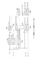
図1は、本発明の実施形態による半導体記憶装置(メモリ装置)の構成例を示すブロック図である。メモリコア120は、ワードラインセレクタ121、センスアンプセレクタ122、メモリセル123、センスアンプ124及びカラムラインセレクタ125を有する。
FIG. 1 is a block diagram showing a configuration example of a semiconductor memory device (memory device) according to an embodiment of the present invention. The
アドレスADDは、アドレス入力回路101を介してアドレスデコーダ102に供給される。アドレスデコーダ102は、アドレスADDを基にデコードし、セレクタ121、122及び125に制御信号を出力する。
The address ADD is supplied to the
セルフリフレッシュタイマ103は、定期的にリフレッシュコマンドrefpzをアービタ104に出力する。チップイネーブル信号/CE1、アウトプットイネーブル信号/OE及びライトイネーブル信号/WEは、コマンド入力回路105を介してコマンドコントローラ106に供給される。上位バイトマスク信号/UBは、マスク解除により上位バイトを有効にし、マスクにより上位バイトを無効にする。下位バイトマスク信号/LBは、マスク解除により下位バイトを有効にし、マスクにより下位バイトを無効にする。コマンドコントローラ106は、信号/CE1,/OE,/WE,/UB,/LBを基に、リードコマンドrdpz又はライトコマンドwrpzをアービタ104に出力する。
The self-
リードコマンドrdpzは、メモリセル123からデータをリードするためのコマンドである。ライトコマンドwrpzは、メモリセル123にデータをライトするためのコマンドである。リフレッシュコマンドrefpzは、メモリセル123をリフレッシュするためのコマンドである。
The read command rdpz is a command for reading data from the
リフレッシュは、DRAMの記憶が失われないように電荷を補充する動作である。半導体記憶装置の一種であるDRAMは、メモリセル123内にコンデンサを有し、コンデンサに電荷を蓄えることによってデータを保持する。この電荷は時間とともに減少するため、放っておくと一定時間で放電しきって情報を失ってしまう。これを防ぐため、DRAMには一定時間ごとに再び電荷を注入するリフレッシュ動作を行う必要がある。
The refresh is an operation for replenishing charges so that the memory of the DRAM is not lost. A DRAM, which is a kind of semiconductor memory device, has a capacitor in the
リフレッシュ中には、リード及びライトを行うことができない。逆に、リード又はライト中に、リフレッシュを行うことができない。したがって、リフレッシュ中に、リードコマンドrdpz又はライトコマンドwrpzが発生すると、リード又はライト動作は待機させられる。逆に、リード又はライト中に、リフレッシュコマンドrefpzが発生すると、リフレッシュ動作は待機させられる。アービタ104は、リフレッシュコマンドrefpz、リードコマンドrdpz及びライトコマンドwrpzを発生順に応じてタイミングコントローラ107に出力する。
During refresh, reading and writing cannot be performed. Conversely, refresh cannot be performed during read or write. Therefore, if a read command rdpz or a write command wrpz is generated during refresh, the read or write operation is put on standby. Conversely, if a refresh command refpz occurs during reading or writing, the refresh operation is put on standby. The
タイミングコントローラ107は、リフレッシュコマンドrefpz、リードコマンドrdpz及びライトコマンドwrpzに応じて、ワードラインセレクタ121、センスアンプセレクタ122及びカラムラインセレクタ125に制御信号mwlonz,msaez等を出力する。制御信号mwlonzはワードラインセレクタ121に供給され、制御信号msaezはセンスアンプセレクタ122に供給される。
The
上位バイトマスク信号/UB及び下位バイトマスク信号/LBは、バイトマスク入力回路108を介してバイトマスクコントローラ109に供給される。バイトマスクコントローラ109は、その信号に応じてカラムラインセレクタ125に制御信号を出力する。
The upper byte mask signal / UB and the lower byte mask signal / LB are supplied to the
2次元配列されたメモリセル123は、ワードライン及びカラムラインにより特定される。ワードラインセレクタ121は、制御信号に応じて、ワードラインを選択して活性化する。カラムラインセレクタ125は、制御信号に応じて、カラムラインを選択する。ライトコマンドwrpzが発生すると、特定されたメモリセル123にデータをライトして記憶することができる。リードコマンドrdpzが発生すると、特定されたメモリセル123からデータをリードすることができる。メモリセル123は、リードコマンドrdpz又はライトコマンドwrpzに応じてデータアクセスされる。センスアンプセレクタ122は、制御信号に応じて、センスアンプ124を活性化する。センスアンプ124は、メモリセル123のビットライン上の信号(データ)を増幅する。
The two-dimensionally arranged
リードコマンドrdpzが発生した場合、リードデータコントローラ112は、カラムラインセレクタ125を介してメモリセル123からデータをリードし、データI/O回路110を介して外部にデータDQを出力する。
When the read command rdpz is generated, the
ライトコマンドwrpzが発生した場合、ライトデータコントローラ111は、データDQをデータI/O回路110を介して入力し、カラムラインセレクタ125を介してメモリセル123にデータをライトする。
When the write command wrpz is generated, the
図2は、図1のバイトマスク入力回路108、バイトマスクコントローラ109、データI/O回路110、ライトデータコントローラ111及びカラムラインセレクタ125の構成例を示す。
FIG. 2 shows a configuration example of the byte
コマンドジェネレータ201は、ライトイネーブル信号/WEを基にライトコマンド信号wrpxを出力する。ライトコマンド信号wrpxは、ライトイネーブル信号/WEの立ち下がりを遅延させた時点で発生するパルス信号である。タイミングディレイ回路204は、ライトコマンド信号wrpxを遅延させてタイミング調整したライトコマンド信号bwrpzを出力する。
The
マスク入力制御回路202は、データバイトマスク信号/UB,/LBを基に信号dmlpzを生成する。マスク入力回路205は、信号/LB,/UB,dmlpz,wrpx,bwrpzを基に信号dmx(/UB)及びdmx(/LB)を出力する。マスク入力回路205の詳細は、後に図3(B)を参照しながら説明する。カラムライン制御回路206は、信号dmx(/UB)及びdmx(/LB)を基に信号clz(/UB)及びclz(/LB)を出力する。
The mask
データ入力制御回路203は、ライトイネーブル信号/WE及びデータバイトマスク信号/UB,/LBを基に上位バイト信号wdlupz,pwdlupz及び下位バイト信号wdllpz,pwdllpzを出力する。
The data
上位バイトデータ入力回路207Uは、信号/UB,pwdluzp,wdlupz,wdllpz,bwrpzに応じて、上位バイトデータDQ(/UB)を入力して上位バイトデータcdbz(/UB)を出力する。下位バイトデータ入力回路207Lは、信号/LB,pwdllzp,wdlupz,wdllpz,bwrpzに応じて、下位バイトデータDQ(/LB)を入力して下位バイトデータcdbz(/LB)を出力する。データ入力回路207U,207Lの詳細は、後に図3(A)を参照しながら説明する。
Upper byte
上位バイトカラムライン選択回路208Uは、信号clz(/UB)に応じて、データcdbz(/UB)を入力してビットライン信号bl(/UB)及び/bl(/UB)を出力する。下位バイトカラムライン選択回路208Lは、信号clz(/LB)に応じて、データcdbz(/LB)を入力してビットライン信号bl(/LB)及び/bl(/LB)を出力する。具体的には、カラムライン選択回路208U,208Lは、データバス(信号cdbz)とメモリセル124のビットライン(信号bl,/bl)とを選択的に接続する。
The upper byte column
図3(A)は、図2のデータ入力回路207U及び207Lの構成例を示す。まず、上位バイトデータ入力回路207Uの構成例を説明する。データ取り込みゲート301Uは、信号pwdlupzのゲート制御により、入力される上位バイトデータDQ(/UB)をバッファ302Uにバッファリングする。データ転送ゲート303Uは、信号wdlupz又はwdllpzの論理和信号のゲート制御により、バッファ302Uのデータを入力してバッファ304Uにバッファリングする。データライトゲート305Uは、信号bwrpzのゲート制御により、バッファ304Uのデータをデータバスに信号cdbz(/UB)として出力する。
FIG. 3A shows a configuration example of the
次に、下位バイトデータ入力回路207Lの構成例を説明する。データ取り込みゲート301Lは、信号pwdllpzのゲート制御により、入力される下位バイトデータDQ(/LB)をバッファ302Lにバッファリングする。データ転送ゲート303Lは、信号wdlupz又はwdllpzの論理和信号のゲート制御により、バッファ302Lのデータを入力してバッファ304Lにバッファリングする。データライトゲート305Lは、信号bwrpzのゲート制御により、バッファ304Lのデータをデータバスに信号cdbz(/LB)として出力する。
Next, a configuration example of the lower byte
以下、データ取り込みゲート301U,301Lを総称してデータ取り込みゲートGD1、データ転送ゲート303U,303Lを総称してデータ転送ゲートGD2、データライトゲート305U,305Lを総称してデータライトゲートGD3という。
Hereinafter, the
図3(B)は、図2のマスク入力回路205の構成例を示す。まず、上位バイトマスク信号/UBの回路について説明する。マスク取り込みゲート311Uは、信号dmlpzのゲート制御により、入力される上位バイトマスク信号/UBをバッファ312Uにバッファリングする。マスク転送ゲート313Uは、信号bwrpzのゲート制御により、バッファ312Uのマスク信号を入力してバッファ314Uにバッファリングする。マスクライトゲート315Uは、信号wrpxのゲート制御により、バッファ314Uのマスク信号を信号dmx(/UB)として出力する。
FIG. 3B shows a configuration example of the
次に、下位バイトマスク信号/LBの回路について説明する。マスク取り込みゲート311Lは、信号dmlpzのゲート制御により、入力される下位バイトマスク信号/LBをバッファ312Lにバッファリングする。マスク転送ゲート313Lは、信号bwrpzのゲート制御により、バッファ312Lのマスク信号を入力してバッファ314Lにバッファリングする。マスクライトゲート315Lは、信号wrpxのゲート制御により、バッファ314Lのマスク信号を信号dmx(/LB)として出力する。
Next, the circuit of the lower byte mask signal / LB will be described. The
以下、マスク取り込みゲート311U,311Lを総称してマスク取り込みゲートGM1、マスク転送ゲート313U,313Lを総称してマスク転送ゲートGM2、マスクライトゲート315U,315Lを総称してマスクライトゲートGM3という。
Hereinafter, the
図4は、図2のデータ入力制御回路203及びデータ入力回路207Uの参考例による構成例を示す。図4は、上位バイトの回路の構成を示すが、下位バイトの回路の構成も同様である。図5は、図4の回路の動作を説明するためのタイミングチャートである。図5において、ライトのサイクルC1及びサイクルC2は、アドレスADD(図1)の切り替えに応じて決まる。第1のサイクルC1は第1のライト動作WR1のサイクル、第2のサイクルC2は第2のライト動作WR2のサイクルである。
FIG. 4 shows a configuration example according to a reference example of the data
CDINBUF回路401は、データDQ(/UB)をバッファリングしてデータDQ1を出力する。CDINLAT回路402は、信号wdluzの制御に応じて、データDQ1を入力し、セットアップ/ホールドのタイミング調整してデータDQ2を出力する。
The
CWDLGEN(/UB)回路403は、ライトイネーブル信号/WE、チップイネーブル信号/CE1及び上位バイトマスク信号/UBを入力し、信号wdluzを出力する。具体的には、CWDLGEN(/UB)回路403は、チップイネーブル信号/CE1及びライトイネーブル信号/WEが活性化(ローレベル)しておりかつ上位バイトマスク信号/UBがマスク解除(ローレベル)である期間を活性化(ローレベル)させる第1の信号(破線で示す信号wdluz)を生成し、その第1の信号が非活性化(ハイレベル)から活性化(ローレベル)に変化する変化点を遅延させた信号を第1の遅延信号wdluzとして出力する。
The CWDLGEN (/ UB)
CWDLPGEN(/UB)回路404は、信号wdluzを入力し、信号pwdlupz及びwdlupzを出力する。信号wdlupzは、信号wdluzがハイレベルからローレベルに変化する変化点においてパルスが生成されるデータ転送ゲートパルス信号である。信号pwdlupzは、信号wdluzがローレベルからハイレベルへ変化する変化点においてパルスが生成されるデータ取り込みゲートパルス信号である。
The CWDLPGEN (/ UB)
CWDBSW回路405は、図3(A)の回路に対応し、信号bwrpz,pwdlupz,wdlupz,wdllpzの制御に応じて、データDQ2を入力し、データcdbzを出力する。信号bwrpzは、ライトイネーブル信号/WEの立ち下がり点を遅延させた点でパルスが生成される。図3(A)に示すように、データ取り込みゲートGD1は、信号pwdlupzのゲート制御に応じて、データDQ2をバッファ302Uに入力する。データ転送ゲートGD2は、信号wdlupz及びwdllpzの論理和信号のゲート制御に応じて、バッファ304Uにデータを入力する。データライトゲートGD3は、信号bwrpzの制御に応じて、バッファ304Uのデータをデータバスに出力する。
A
以上のように、CDINBUF回路401で入力データDQ(/UB)のハイレベル/ローレベル判定を行い、CDINLAT回路402でセットアップ/ホールドのタイミング調整を行い、CWDBSW回路405でデータバスへのデータ転送を行う。CWDBSW回路405では、信号pwdlupzで上位バイトデータDQ2をバッファ302Uに取り込み、信号wdlupz又はwdllpzでバッファ304Uへデータの転送を行う。データバスへのデータ転送は、データライトの実行時に信号bwrpzでデータバスに転送することでタイミング調整を行っている。これらの取り込み及び転送制御を行っているのがCWDLGEN回路403及びCWDLPGEN回路404であり、CWDLGEN回路403でライト動作を行うべきか、ライトせずに待つかを判定するためのフィルタを構成しており、その出力信号wdluzの立ち下がり及び立ち上がりそれぞれのエッジからデータ転送パルス信号wdlupz及びデータ取り込みパルス信号pwdlupzを生成している。このため、ライト動作をしない場合にデータの取り込みでデータ破壊を行わないようにするとデータの転送もされなくなるので、ライト動作の実行の有無の境界とデータの取り込み及びデータ転送の有無を高精度に調整する必要がある。
As described above, the
本来であれば、ライトイネーブル信号/WEが立ち下がる以前に、バイトマスク信号/UB,/LBが変化して確定している必要がある。しかし、電源電圧のばらつき変動や素子のばらつき変動等により、図5に示すように、バイトマスク信号/UB,/LBの変化がライトイネーブル信号/WEの立ち下がりよりも遅れてしまうことがある。この場合に、誤動作が生じないように制御する必要がある。 Originally, before the write enable signal / WE falls, the byte mask signals / UB and / LB need to be changed and fixed. However, due to fluctuations in power supply voltage variations, element variations, etc., changes in the byte mask signals / UB, / LB may be delayed from the fall of the write enable signal / WE, as shown in FIG. In this case, it is necessary to perform control so that no malfunction occurs.
正常な場合には、ライトイネーブル信号/WEの立ち下がりとバイトマスク信号/UB,/LBの変化点が同じである。この場合は、例えば、サイクルC1において、データ取り込みゲート信号pwdlupzによりバッファ302Uにデータを取り込む。そして、その次のサイクルC2において、データ転送信号wdlupz又はwdllpzによりそのデータをバッファ304Uに転送し、かつその後のデータライト信号bwrpzによりそのデータをデータバスに出力してメモリセルにライトする。これがライトサイクルである。
When normal, the falling edge of the write enable signal / WE and the changing point of the byte mask signals / UB and / LB are the same. In this case, for example, in the cycle C1, data is taken into the
バイトマスク信号/UB,/LBの切り替えがライトイネーブル信号/WEの立ち下がりより遅れてしまったような場合、ライトの初期にマスクすべきバイト(例えば下位バイト)へのライト状態が回路内部に発生してしまう。そのため、本来はライトWR1で下位バイトマスク信号/LBの立ち上がり時点のデータを取り込んではいけないが、現サイクルC1において、データ取り込みゲート信号pwdllpzのパルス501で下位バイトデータDQ(/LB)を取り込んでしまい、次サイクルC2において、データ転送ゲート信号wdllpzのパルス502でデータを転送し、データライトゲート信号bwrpzのパルス503でデータバスへデータが出力されてしまう。パルス503以降でライト動作を行ってメモリセルにデータを書き込んでしまうため、データが破壊される。すなわち、パルス501の時点では、下位バイトデータDQ(/LB)が供給されていないので、パルス501により取り込んだデータは不定(不正)データである。そのデータをメモリセルを書き込んでしまうために、データ破壊が生じる。下記の本実施形態では、上記の問題点を解決することができる。
When switching of the byte mask signal / UB, / LB is delayed from the falling edge of the write enable signal / WE, a write state to a byte (for example, a lower byte) to be masked at the initial stage of writing occurs in the circuit Resulting in. Therefore, originally, the data at the rising edge of the lower byte mask signal / LB must not be captured by the write WR1, but the lower byte data DQ (/ LB) is captured by the
図6は、図2のデータ入力制御回路203及びデータ入力回路207Uの本実施形態による構成例を示す。図6は、上位バイトの回路の構成を示すが、下位バイトの回路の構成も同様である。図7は、図6の回路の動作を説明するためのタイミングチャートである。図7において、ライトのサイクルC1及びサイクルC2は、アドレスADD(図1)の切り替えに応じて決まる。第1のサイクルC1は第1のライト動作WR1のサイクル、第2のサイクルC2は第2のライト動作WR2のサイクルである。
FIG. 6 shows a configuration example according to this embodiment of the data
図6の回路が図4の回路に比べて異なる点を説明する。CWDLGEN(/UB)回路603及びCWDLPGEN(/UB)回路604は、図4のCWDLGEN回路(/UB)403及びCWDLPGEN(/UB)回路404の代わりに設けられる。
The difference between the circuit of FIG. 6 and the circuit of FIG. 4 will be described. The CWDLGEN (/ UB)
CWDLGEN(/UB)回路603は、ライトイネーブル信号/WE、チップイネーブル信号/CE1及び上位バイトマスク信号/UBを入力し、信号wdluz及びpwdluzを出力する。具体的には、CWDLGEN(/UB)回路603は、チップイネーブル信号/CE1及びライトイネーブル信号/WEが活性化(ローレベル)しておりかつ上位バイトマスク信号/UBがマスク解除(ローレベル)である期間を活性化(ローレベル)させる第1の信号(破線で示す信号wdluz)を生成し、その第1の信号が非活性化(ハイレベル)から活性化(ローレベル)に変化する変化点を第1の遅延時間遅延させた信号を第1の遅延信号wdluzとして出力する。また、CWDLGEN(/UB)回路603は、上記の第1の信号(破線で示す信号pwdluz)が非活性化(ハイレベル)から活性化(ローレベル)に変化する変化点を上記第1の遅延時間より長い第2の遅延時間遅延させた信号を第2の遅延信号pwdluzとして出力する。
The CWDLGEN (/ UB)
CWDLPGEN(/UB)回路604は、信号wdluz及びpwdluzを入力し、信号pwdlupz及びwdlupzを出力する。信号wdlupzは、信号wdluzがハイレベルからローレベルに変化する変化点においてパルスが生成されるデータ転送ゲートパルス信号である。信号pwdlupzは、信号pwdluzがローレベルからハイレベルへ変化する変化点においてパルスが生成されるデータ取り込みゲートパルス信号である。
The CWDLPGEN (/ UB)
本実施形態では、CWDLGEN回路603のフィルタをデータ取り込み信号とデータ転送信号で個別に用意する。そのため、データの転送(信号wdllpz)を行うがデータの取り込み(信号pwdllpz)を行わないという状態を実現することができる。このため、図4及び図5の参考例のように次データがデータバスへスルーしてしまいデータ破壊が発生するという現象を防止することができる。その詳細は、後に図8(A)〜(C)を参照しながら説明する。
In the present embodiment, the filters of the
図7において、サイクルC1では、下位バイトマスク信号がハイレベル(マスク状態)であり、下位バイトデータDQ(/LB)が供給されていない。下位バイトデータ取り込みパルス701が発生しないので、不定(不正)データを取り込んでメモリセルにライトすることを防止できる。具体的には、次のサイクルC2でデータ転送パルス702及びデータライトパルス703が発生し、データバスに前のデータが供給されるが、下位バイトマスク信号/LBがハイレベルとしてカラムライン選択回路208L(図2)に供給されているので、データバスはメモリセルに接続されない。結果的に、メモリセルへのライトは行われず、データ破壊は生じない。
In FIG. 7, in cycle C1, the lower byte mask signal is at the high level (mask state), and the lower byte data DQ (/ LB) is not supplied. Since the lower byte
そして、下位バイト取り込みゲート信号pwdllpzは、サイクルC2において、パルスが発生し、下位バイトデータDQ(/LB)が取り込まれる。そして、さらに次のサイクルにおいて、そのデータがデータ転送ゲート信号により転送され、データライトゲート信号によりデータバスに供給される。そして、下位バイトマスク信号/LBがローレベルとしてカラムライン選択回路208L(図2)に供給され、データバスはメモリセルに接続される。結果的に、メモリセルへ正常なデータをライトすることができる。
The lower byte fetch gate signal pwdllpz is pulsed in cycle C2 and lower byte data DQ (/ LB) is fetched. In the next cycle, the data is transferred by the data transfer gate signal and supplied to the data bus by the data write gate signal. Then, the lower byte mask signal / LB is supplied to the column
以上のように、サイクルC2において、下位バイトのデータ転送が行われ、マスク信号のハイレベルが取り込めればデータバスはメモリセルに接続されずにデータを実際にメモリセルに書き込むことはないのでデータ破壊が生じない。そのため、ライトコマンドの発生自体の制限を緩くしてもデータ破壊を起こさず、ライトサイクル動作の鈍化を防止することが可能である。 As described above, in cycle C2, data transfer of the lower byte is performed, and if the high level of the mask signal is captured, the data bus is not connected to the memory cell and data is not actually written to the memory cell. No destruction occurs. For this reason, even if the restriction on the generation of the write command itself is relaxed, it is possible to prevent the write cycle operation from slowing without causing data destruction.
このように、マスク取り込み、データ取り込み、データライト、データ転送の優先順位を適切なものとすることによってライトコマンドが発生してもデータ破壊が発生しないため、ライト動作の遅延を防止することができる。 In this way, by making the priority order of mask capture, data capture, data write, and data transfer appropriate, even if a write command occurs, data destruction does not occur, so that a delay in write operation can be prevented. .
図8(A)〜(C)は、ライト動作例を示す。サイクル毎に、ライト動作WR0,WR1,WR2が順に行われる例を説明する。 8A to 8C show examples of the write operation. An example in which the write operations WR0, WR1, and WR2 are sequentially performed for each cycle will be described.
図8(A)は、基本のライト動作例を示す。ライトイネーブル信号/WEにおいて、ライト動作WR1及びWR2のローレベル期間が十分に長い場合の正常動作を示す。 FIG. 8A shows a basic write operation example. In the write enable signal / WE, normal operation when the low level period of the write operations WR1 and WR2 is sufficiently long is shown.
ライトイネーブル信号/WEがライト動作WR1のために立ち下がると、ライト動作WR0のデータ転送GD2[0]が行われ、ライト動作WR1のマスク取り込みGM1[1]が行われる。次に、ライト動作WR0のマスクライトGM3[0]が行われる。次に、ライト動作WR0のデータライトGD3[0]が行われ、ライト動作WR1のマスク転送GM2[1]が行われる。その後、ライト動作WR0のライトコマンドWR[0]によりメモリセルにデータがライトされる。また、ライトイネーブル信号/WEが立ち上がると、ライト動作WR1のデータ取り込みGD1[1]が行われる。 When the write enable signal / WE falls for the write operation WR1, the data transfer GD2 [0] of the write operation WR0 is performed, and the mask capture GM1 [1] of the write operation WR1 is performed. Next, the mask write GM3 [0] of the write operation WR0 is performed. Next, data write GD3 [0] for write operation WR0 is performed, and mask transfer GM2 [1] for write operation WR1 is performed. Thereafter, data is written to the memory cell by the write command WR [0] of the write operation WR0. Further, when the write enable signal / WE rises, the data acquisition GD1 [1] of the write operation WR1 is performed.
次に、ライトイネーブル信号/WEがライト動作WR2のために立ち下がると、ライト動作WR1のデータ転送GD2[1]が行われ、ライト動作WR2のマスク取り込みGM1[2]が行われる。次に、ライト動作WR1のマスクライトGM3[1]が行われる。次に、ライト動作WR1のデータライトGD3[1]が行われ、ライト動作WR2のマスク転送GM2[2]が行われる。その後、ライト動作WR1のライトコマンドWR[1]によりメモリセルにデータがライトされる。また、ライトイネーブル信号/WEが立ち上がると、ライト動作WR2のデータ取り込みGD1[2]が行われる。 Next, when the write enable signal / WE falls for the write operation WR2, the data transfer GD2 [1] of the write operation WR1 is performed, and the mask capture GM1 [2] of the write operation WR2 is performed. Next, the mask write GM3 [1] of the write operation WR1 is performed. Next, data write GD3 [1] of write operation WR1 is performed, and mask transfer GM2 [2] of write operation WR2 is performed. Thereafter, data is written to the memory cell by the write command WR [1] of the write operation WR1. When the write enable signal / WE rises, data capture GD1 [2] for the write operation WR2 is performed.
図8(B)は、図4の参考例のメモリ装置のライト動作例を示す。ライトイネーブル信号/WEにおいて、ライト動作WR1のローレベル期間が短い場合の誤動作を示す。この場合、ライトイネーブル信号/WEがライト動作WR1のために立ち下がると、ライト動作WR0のデータ転送GD2[0]が行われ、それに重なるようにライト動作WR1のデータ取り込みGD1[1]が行われる。データ転送ゲート信号wdlupzのパルスとデータ取り込みゲート信号pwdlupzのパルスとが時間的に一部重なってしまい、図3(A)のデータ転送ゲートGD2及びデータ取り込みゲートGD1が同時に開いてしまう。その結果、バッファ304Uには、本来ライト動作WR0のデータが格納されなければならないのに、エラーによりライト動作WR1のデータが格納されてしまう。そして、次のデータライトGD3[0]及びライトコマンドWR[0]では、そのライト動作WR1のデータがメモリセルにライトされてしまい、誤動作になる。これは、図5において、データ転送ゲート信号wdlupz及びデータ取り込みゲート信号pwdlupzが共に同じ信号wdluzの立ち下がり及び立ち上がりを基に生成されるためである。すなわち、データ転送ゲート信号wdlupzのパルスが生成されたときには、必ずデータ取り込みゲート信号pwdlupzのパルスも生成されてしまい、ライトイネーブル信号/WEのローレベル期間が短くなると、その両者のパルスが重なってしまうためである。
FIG. 8B shows an example of the write operation of the memory device of the reference example of FIG. In the write enable signal / WE, a malfunction occurs when the low level period of the write operation WR1 is short. In this case, when the write enable signal / WE falls for the write operation WR1, the data transfer GD2 [0] of the write operation WR0 is performed, and the data acquisition GD1 [1] of the write operation WR1 is performed so as to overlap therewith. . The pulse of the data transfer gate signal wdlupz and the pulse of the data capture gate signal pwdlupz partially overlap in time, and the data transfer gate GD2 and the data capture gate GD1 of FIG. As a result, the data for the write operation WR0 must be stored in the
図8(C)は、図6の本実施形態のメモリ装置のライト動作例を示す。ライトイネーブル信号/WEにおいて、ライト動作WR1のローレベル期間が短い場合に誤動作を防止できることを説明する。この場合、ライトイネーブル信号/WEがライト動作WR1のために立ち下がると、ライト動作WR0のデータ転送GD2[0]が行われる。しかし、ライトイネーブル信号/WEのローレベル期間が短いためにライト動作WR1のデータ取り込みGD1[1]が行われない。すなわち、ライトイネーブル信号/WEのローレベル期間が短い場合には、図7において、遅延時間が短い信号wdluzはローレベル期間が生じ、遅延時間が長い信号pwdluzはローレベル期間が生じない。その結果、データ転送ゲート信号wdlupzのパルスが発生してデータ転送GD2[0]を行い、データ取り込みゲート信号pwdlupzのパルスが発生せずにデータ取り込みGD1[1]が行われない。これにより、データ転送ゲートGD2が開き、データ取り込みゲートGD1が閉じるので、バッファ304Uにはライト動作WR0の正常なデータが格納され、データライトGD3[0]及びライトコマンドWR[0]によりそのデータがメモリセルに書き込まれ、正常な動作が保証される。
FIG. 8C shows an example of a write operation of the memory device of this embodiment shown in FIG. In the write enable signal / WE, it will be described that malfunction can be prevented when the low level period of the write operation WR1 is short. In this case, when the write enable signal / WE falls for the write operation WR1, the data transfer GD2 [0] of the write operation WR0 is performed. However, since the low level period of the write enable signal / WE is short, the data capture GD1 [1] of the write operation WR1 is not performed. That is, when the low level period of the write enable signal / WE is short, in FIG. 7, the signal wdluz having a short delay time has a low level period, and the signal pwdluz having a long delay time does not have a low level period. As a result, a data transfer gate signal wdlupz pulse is generated and data transfer GD2 [0] is performed, and no data capture gate signal pwdlupz pulse is generated and data capture GD1 [1] is not performed. As a result, the data transfer gate GD2 is opened and the data fetch gate GD1 is closed, so that the normal data of the write operation WR0 is stored in the
図9は、tBSスペック及びtBWスペックを説明するための図である。上記のように、ライトイネーブル信号/WEの立ち下がり時又はそれよりも前にバイトマスク信号/UB及び/LBが変化して確定していれば、正常なライト動作が行われる。ライトイネーブル信号/WEの立ち下がりの後にバイトマスク信号/UB,/LBが変化したときには、誤動作を防止する必要がある。この際、時間tBS[0]は、ライトイネーブル信号/WEが活性化(ローレベル)してからバイトマスク信号/UB,/LBが変化するまでの間の負の時間である。時間tBW[1]は、バイトマスク信号/UB,/LBが変化してからライトイネーブル信号/WEが非活性化(ハイレベル)するまでの間の時間である。 FIG. 9 is a diagram for explaining the tBS spec and the tBW spec. As described above, if the byte mask signals / UB and / LB change and are determined before or after the fall of the write enable signal / WE, a normal write operation is performed. When the byte mask signals / UB, / LB change after the fall of the write enable signal / WE, it is necessary to prevent malfunction. At this time, the time tBS [0] is a negative time from when the write enable signal / WE is activated (low level) until the byte mask signals / UB and / LB change. Time tBW [1] is the time from when the byte mask signals / UB, / LB change until the write enable signal / WE is deactivated (high level).
図10(A)及び(B)は、図4の参考例のメモリ装置の動作モードを示す。データ転送GD2及びデータ取り込みGD1は、両方行うか又は両方行わないかである。横軸は時間tBS[ns]を示し、0よりも左側が負値を示す。 10A and 10B show operation modes of the memory device of the reference example of FIG. Data transfer GD2 and data capture GD1 are both performed or not performed. The horizontal axis indicates time tBS [ns], and the left side from 0 indicates a negative value.
図10(A)は、データライトGD3をデータ転送GD2及びデータ取り込みGD1よりも優先させる場合を示す。動作モード1、2a、3a、4、5の順に、時間tBS(負値)が小さくなる。
FIG. 10A shows a case where the data write GD3 is prioritized over the data transfer GD2 and the data capture GD1. The time tBS (negative value) decreases in the order of the
動作モード1では、そのサイクルにおいて、データライトGD3、データ転送GD2及びデータ取り込みGD1を行わず、マスク取り込みGM1はマスク信号/UBとしてハイレベルを取り込む。この結果、メモリセルへの書き込みは行なわれず、誤動作(データ破壊)はない。
In
動作モード2aでは、そのサイクルにおいて、データライトGD3を行い、データ転送GD2及びデータ取り込みGD1を行わず、マスク取り込みGM1はマスク信号/UBとしてハイレベルを取り込む。この際、データ転送GD2が行われずに、データライトGD3が行われるため、正しいデータがメモリセルに書き込まれず、データ破壊が生じることがある。 In the operation mode 2a, in the cycle, the data write GD3 is performed, the data transfer GD2 and the data capture GD1 are not performed, and the mask capture GM1 captures the high level as the mask signal / UB. At this time, since the data write GD3 is performed without performing the data transfer GD2, correct data may not be written to the memory cell, and data destruction may occur.
動作モード3aでは、そのサイクルにおいて、データライトGD3、データ転送GD2及びデータ取り込みGD1を行い、マスク取り込みGM1はマスク信号/UBとしてハイレベルを取り込む。この際、図8(B)のように、データ転送GD2及びデータ取り込みGD1が時間的に重なることがあり、誤ったデータをメモリセルにライトしてしまい、データ破壊してしまうことがある。 In the operation mode 3a, data write GD3, data transfer GD2, and data capture GD1 are performed in the cycle, and the mask capture GM1 captures a high level as a mask signal / UB. At this time, as shown in FIG. 8B, the data transfer GD2 and the data take-in GD1 may overlap with each other in time, and erroneous data may be written to the memory cell, thereby destroying the data.
動作モード4では、そのサイクルにおいて、データライトGD3、データ転送GD2及びデータ取り込みGD1を行い、マスク取り込みGM1はマスク信号/UBとして不定値を取り込む。マスク信号/UBとして不定値が取り込まれるので、正しいマスク制御(カラムライン選択)が保証されず、データ破壊が生じることがある。動作モード4は、マスク信号/UBのハイレベル(動作モード1〜3a)とローレベル(動作モード5)の境界であるので、マスク信号/UBが不定値になる。
In
動作モード5では、そのサイクルにおいて、データライトGD3、データ転送GD2及びデータ取り込みGD1を行い、マスク取り込みGM1はマスク信号/UBとしてローレベルを取り込む。この場合は、正常なライト動作が行われる。
In
図10(B)は、データ転送GD2及びデータ取り込みGD1をデータライトGD3よりも優先させる場合を示す。動作モード1、2b、3b、4、5の順に、時間tBS(負値)が小さくなる。動作モード1、4及び5は、図10(A)のものと同じである。また、動作モード3bは、図10(A)の動作モード3aと同様のデータ破壊の可能性がある。
FIG. 10B shows a case where the data transfer GD2 and the data capture GD1 are prioritized over the data write GD3. The time tBS (negative value) decreases in the order of the
動作モード2bでは、そのサイクルにおいて、データライトGD3を行わず、データ転送GD2及びデータ取り込みGD1を行い、マスク取り込みGM1はマスク信号/UBとしてハイレベルを取り込む。この際、データ取り込みGD1及びデータ転送GD2が行われ、データライトGD3が行われないため、バッファ304Uにデータが上書きされてしまい、データ破壊が生じることがある。
In the
図11は、図12〜図15、図17及び図18を説明するためのライト動作例を示す。ライトイネーブル信号/WEは、ライト動作WR1、WR2及びWR3の順にローレベル期間が生じる。この間、マスク信号/LBはハイレベルであるとする。ライト動作WR1では、マスク信号/UBとしてM1、データDQとしてD1が供給される。ライト動作WR2では、マスク信号/UBとしてM2、データDQとしてD2が供給される。ライト動作WR3では、マスク信号/UBとしてM3、データDQとしてD3が供給される。 FIG. 11 shows a write operation example for explaining FIGS. 12 to 15, 17 and 18. The write enable signal / WE has a low level period in the order of the write operations WR1, WR2, and WR3. During this period, the mask signal / LB is assumed to be at a high level. In the write operation WR1, M1 is supplied as the mask signal / UB, and D1 is supplied as the data DQ. In the write operation WR2, M2 is supplied as the mask signal / UB, and D2 is supplied as the data DQ. In the write operation WR3, M3 is supplied as the mask signal / UB and D3 is supplied as the data DQ.
図12は、動作モード5のデータ制御及びマスク制御例を示す。ライトイネーブル信号/WE(ライト動作WR1〜WR3)のローレベル期間が十分に長い場合を示す。
FIG. 12 shows an example of data control and mask control in the
ライトイネーブル信号/WEの立ち下がりによりライト動作WR1が指示されると、データ転送ゲートGD2のスイッチが閉じデータD0がバッファ304Uに格納され、マスク取り込みゲートGM1のスイッチが閉じマスク信号M1がバッファ312Uに格納される。次に、データライトゲートGD3のスイッチが閉じデータD0がデータバスに出力され、マスクライトゲートGM3のスイッチが閉じマスク信号M0が出力される。次に、マスク転送ゲートGM2のスイッチが閉じマスク信号M1がバッファ314Uに格納される。次に、データ取り込みゲートGD1のスイッチが閉じデータD1がバッファ302Uに格納される。ライト動作WR0(データD0)は、正常に行われる。
When the write operation WR1 is instructed by the fall of the write enable signal / WE, the switch of the data transfer gate GD2 is closed and the data D0 is stored in the
ライトイネーブル信号/WEの立ち下がりによりライト動作WR2が指示されると、データ転送ゲートGD2のスイッチが閉じデータD1がバッファ304Uに格納され、マスク取り込みゲートGM1のスイッチが閉じマスク信号M2がバッファ312Uに格納される。次に、データライトゲートGD3のスイッチが閉じデータD1がデータバスに出力され、マスクライトゲートGM3のスイッチが閉じマスク信号M1が出力される。次に、マスク転送ゲートGM2のスイッチが閉じマスク信号M2がバッファ314Uに格納される。次に、データ取り込みゲートGD1のスイッチが閉じデータD2がバッファ302Uに格納される。ライト動作WR1(データD1)は、正常に行われる。
When the write operation WR2 is instructed by the fall of the write enable signal / WE, the switch of the data transfer gate GD2 is closed and the data D1 is stored in the
ライトイネーブル信号/WEの立ち下がりによりライト動作WR3が指示されると、データ転送ゲートGD2のスイッチが閉じデータD2がバッファ304Uに格納され、マスク取り込みゲートGM1のスイッチが閉じマスク信号M3がバッファ312Uに格納される。次に、データライトゲートGD3のスイッチが閉じデータD2がデータバスに出力され、マスクライトゲートGM3のスイッチが閉じマスク信号M2が出力される。次に、マスク転送ゲートGM2のスイッチが閉じマスク信号M3がバッファ314Uに格納される。次に、データ取り込みゲートGD1のスイッチが閉じデータD3がバッファ302Uに格納される。ライト動作WR2(データD2)は、正常に行われる。
When the write operation WR3 is instructed by the fall of the write enable signal / WE, the switch of the data transfer gate GD2 is closed and the data D2 is stored in the
図13は、動作モード1のデータ制御及びマスク制御例を示す。基本的には、図12と同じであり、異なる点を説明する。ライトイネーブル信号/WE(ライト動作WR2)のローレベル期間が短い場合を示す。
FIG. 13 shows an example of data control and mask control in
ライトイネーブル信号/WEの立ち下がりによりライト動作WR2が指示されると、データ転送ゲートGD2のスイッチが開いたままで、マスク取り込みゲートGM1のスイッチが閉じマスク信号M2がバッファ312Uに格納される。次に、データライトゲートGD3のスイッチが開いたままで、マスクライトゲートGM3のスイッチが開いたままである。次に、マスク転送ゲートGM2のスイッチが開いたままである。次に、データ取り込みゲートGD1のスイッチが開いたままである。このサイクルではライト動作WR1(データD1)が行われず、次のサイクルでライト動作WR1(データD1)が行われる。
When the write operation WR2 is instructed by the fall of the write enable signal / WE, the switch of the mask capture gate GM1 is closed while the switch of the data transfer gate GD2 is kept open, and the mask signal M2 is stored in the
図14は、動作モード2aのデータ制御及びマスク制御例を示す。基本的には、図12と同じであり、異なる点を説明する。ライトイネーブル信号/WE(ライト動作WR2)のローレベル期間が中間値付近の場合を示す。 FIG. 14 shows an example of data control and mask control in the operation mode 2a. Basically, it is the same as FIG. 12, and different points will be described. The case where the low level period of the write enable signal / WE (write operation WR2) is near the intermediate value is shown.
ライトイネーブル信号/WEの立ち下がりによりライト動作WR2が指示されると、データ転送ゲートGD2のスイッチが開いたままで、マスク取り込みゲートGM1のスイッチが閉じマスク信号M2がバッファ312Uに格納される。次に、データライトゲートGD3のスイッチが閉じデータD0がデータバスに出力され、マスクライトゲートGM3のスイッチが閉じマスク信号M1が出力される。次に、マスク転送ゲートGM2のスイッチが閉じマスク信号M2がバッファ314Uに格納される。次に、データ取り込みゲートGD1のスイッチが開いたままである。
When the write operation WR2 is instructed by the fall of the write enable signal / WE, the switch of the mask capture gate GM1 is closed while the switch of the data transfer gate GD2 is kept open, and the mask signal M2 is stored in the
このサイクルでは、誤ったデータD0をマスク信号M1でライトし、データ破壊が生じる。この次のサイクルでは、マスク信号がハイレベルであり、データD1のデータバスがメモリセルに接続されないので、メモリセルへのライトは行われない。したがって、データD1のライトが実行されず、データが破壊される。 In this cycle, erroneous data D0 is written with the mask signal M1, and data destruction occurs. In this next cycle, since the mask signal is at a high level and the data bus of data D1 is not connected to the memory cell, writing to the memory cell is not performed. Therefore, the data D1 is not written and the data is destroyed.
図15は、動作モード2bのデータ制御及びマスク制御例を示す。基本的には、図12と同じであり、異なる点を説明する。ライトイネーブル信号/WE(ライト動作WR2)のローレベル期間が中間値付近の場合を示す。
FIG. 15 shows an example of data control and mask control in the
ライトイネーブル信号/WEの立ち下がりによりライト動作WR2が指示されると、データ転送ゲートGD2のスイッチが閉じデータD1がバッファ304Uに格納され、マスク取り込みゲートGM1のスイッチが閉じマスク信号M2がバッファ312Uに格納される。次に、データライトゲートGD3のスイッチが開いたままで、マスクライトゲートGM3のスイッチが開いたままである。次に、マスク転送ゲートGM2のスイッチが開いたままである。次に、データ取り込みゲートGD1のスイッチが閉じデータD2がバッファ302Uに格納される。
When the write operation WR2 is instructed by the fall of the write enable signal / WE, the switch of the data transfer gate GD2 is closed and the data D1 is stored in the
このサイクルでは、データライトゲートGD3のスイッチが開いたままで、データD0が更新され、新たなデータ書き込みは行われない。次のサイクルでは、データD2がメモリセルに書き込まれる。この結果、ライト動作WR1(データD1)がスキップされたことになり、データ破壊が生じる。 In this cycle, the data D0 is updated while the switch of the data write gate GD3 is kept open, and no new data is written. In the next cycle, data D2 is written into the memory cell. As a result, the write operation WR1 (data D1) is skipped, and data destruction occurs.
以上のように、図10(A)において、データライトGD3が開始する動作モード2aの状態ではデータ転送GD2が行われないのでデータが破壊される。動作モード3aの領域では、動作モード2aと3aの境界でデータ取り込みパルスとデータ転送パルスが同時に発生することで次サイクルのデータがスルーしてしまい、バッファ304Uのデータを破壊する。動作モード4では、マスク取り込みGM1が不安定で意図したライト動作が実現できない。動作モード5ではマスク取り込みGM1、データ取り込みGD1、データ転送GD2が正常に実行でき、意図したライト動作が実行される。
As described above, in FIG. 10A, in the state of the operation mode 2a where the data write GD3 starts, the data transfer GD2 is not performed, so the data is destroyed. In the region of the operation mode 3a, the data fetch pulse and the data transfer pulse are simultaneously generated at the boundary between the operation modes 2a and 3a, whereby the data of the next cycle is passed through and the data in the
図16は、図6の本実施形態のメモリ装置の動作モードを示す。データ取り込みGD1、データライトGD3及びデータ転送GD2の順に、発生優先度が高くなっていく。横軸は時間tBS[ns]を示し、0よりも左側が負値を示す。動作モード1、2c、2d、3、4、5の順に、時間tBS(負値)が小さくなる。動作モード1、3、4及び5は、図10(A)のものと同じである。
FIG. 16 shows an operation mode of the memory device of this embodiment shown in FIG. The generation priority increases in the order of data fetch GD1, data write GD3, and data transfer GD2. The horizontal axis indicates time tBS [ns], and the left side from 0 indicates a negative value. The time tBS (negative value) decreases in the order of the
動作モード2cでは、そのサイクルにおいて、データ転送GD2を行い、データライトGD3及びデータ取り込みGD1を行わず、マスク取り込みGM1はマスク信号/UBとしてハイレベルを取り込む。この詳細は、後に図17を参照しながら説明する。
In the
動作モード2dでは、そのサイクルにおいて、データライトGD3及びデータ転送GD2を行い、データ取り込みGD1を行わず、マスク取り込みGM1はマスク信号/UBとしてハイレベルを取り込む。この詳細は、後に図18を参照しながら説明する。
In the
動作モード3では、図8(B)のように、データ転送GD2[0]及びデータ取り込みGD1[1]が重なってデータ破壊することはない。その場合は、図8(C)に示すように、データ取り込みGD1[1]が発生せず、動作モード2dとなる。動作モード3では、データ転送GD2[0]及びデータ取り込みGD1[1]が重ならないで実行されるので、データ破壊は生じない。
In the
図17は、動作モード2cのデータ制御及びマスク制御例を示す。基本的には、図12と同じであり、異なる点を説明する。ライトイネーブル信号/WE(ライト動作WR2)のローレベル期間が中間値付近の場合を示す。
FIG. 17 shows an example of data control and mask control in the
ライトイネーブル信号/WEの立ち下がりによりライト動作WR2が指示されると、データ転送ゲートGD2のスイッチが閉じデータD1がバッファ304Uに格納され、マスク取り込みゲートGM1のスイッチが閉じマスク信号M2がバッファ312Uに格納される。次に、データライトゲートGD3のスイッチが開いたままで、マスクライトゲートGM3のスイッチが開いたままである。次に、マスク転送ゲートGM2のスイッチが開いたままである。次に、データ取り込みゲートGD1のスイッチが開いたままである。このサイクルではライト動作WR1(データD1)が行われず、次のサイクルでライト動作WR1(データD1)が行われる。
When the write operation WR2 is instructed by the fall of the write enable signal / WE, the switch of the data transfer gate GD2 is closed and the data D1 is stored in the
図18は、動作モード2dのデータ制御及びマスク制御例を示す。基本的には、図12と同じであり、異なる点を説明する。ライトイネーブル信号/WE(ライト動作WR2)のローレベル期間が中間値付近の場合を示す。
FIG. 18 shows an example of data control and mask control in the
ライトイネーブル信号/WEの立ち下がりによりライト動作WR2が指示されると、データ転送ゲートGD2のスイッチが閉じデータD1がバッファ304Uに格納され、マスク取り込みゲートGM1のスイッチが閉じマスク信号M2がバッファ312Uに格納される。次に、データライトゲートGD3のスイッチが閉じデータD1がデータバスに出力され、マスクライトゲートGM3のスイッチが閉じマスク信号M1が出力される。次に、マスク転送ゲートGM2のスイッチが閉じマスク信号M2がバッファ314Uに格納される。次に、データ取り込みゲートGD1のスイッチが開いたままである。
When the write operation WR2 is instructed by the fall of the write enable signal / WE, the switch of the data transfer gate GD2 is closed and the data D1 is stored in the
このサイクルでは、ライト動作WR1(データD1)は、正常に行われる。次のサイクルでは、マスク信号がハイレベルになり、データバス及びメモリセルが接続されないので、データD1はメモリセルにライトされない。結果として、データD0及びD1を正常にライトすることができる。 In this cycle, the write operation WR1 (data D1) is normally performed. In the next cycle, the mask signal becomes high level, and the data bus and the memory cell are not connected, so that the data D1 is not written to the memory cell. As a result, the data D0 and D1 can be normally written.
以上のように、本実施形態において、動作モード1は、データライトGD3を行わず、データ転送GD2も行わない。動作モード2cは、データライトGD3は行わないが、次のライトに備えてデータ転送GD2を行う。動作モード2dは、マスク信号がハイレベルでライトコマンドは認識するが実際の書き込みは行わない。その際、バイトマスク信号の立ち上がり時のデータは取り込まない。動作モード3は、マスク信号がハイレベルでライトコマンドは認識するが実際の書き込みは行わない。その際、バイトマスク信号の立ち上がり時のデータは取り込む。動作モード4は、不定値のマスク信号の誤取り込みでライト動作を行うためにデータ破壊が生じる。動作モード5は、バイトマスク信号のローレベルに対応するデータを取り込み、ライト動作を実行する。
As described above, in the present embodiment, the
データ破壊を行うのは動作モード4であるが、電源電圧変動等によりタイミングが変動することにより、マスク取り込みGM1のタイミングが変動する。そのため、条件によってはライトなし(No WR)となったり、ライト(WR)となったり挙動が不安定となる。ライトなし(No WR)の場合にはマスク信号としてハイレベルが取り込めていれば、データを取り込んでしまったとしても、実際にはデータの書き込みは行われない。ライト(WR)の場合にはデータが取り込めていることが保障されていることからマスク信号のローレベルに相当するデータの書き込みが行われる。
Although the data destruction is performed in the
つまり、ライト動作を行わない場合には半導体記憶装置内部のデータは状態を維持し、ライト動作を行う場合にはライトコマンドとして認識された場合に相当するデータの書き込みが行われる。データの取り込みや転送を行っていないにも関わらずライト動作をしてしまうということを防ぐことができる。 That is, when the write operation is not performed, the data in the semiconductor memory device maintains the state, and when the write operation is performed, data corresponding to the case where it is recognized as a write command is written. It is possible to prevent a write operation from being performed even when data is not captured or transferred.
図10(A)では動作モード5のマスク取り込みのタイミングのみばらつくような図となっているが、実際にはデータ転送GD2(動作モード1〜2a間)、データライトGD3(動作モード2a〜3a間)、データ取り込みGD1(動作モード3a〜4間)も変動する。しかし、これらの位置が変動しても、ライトなし(No WR)がライト(WR)となったり、ライト(WR)がライトなし(No WR)となることはなく、マスク取り込みタイミングの変動(動作モード5)の分だけに誤動作の生じる期間を抑えることが可能となる。図16の場合も同様である。
In FIG. 10A, only the mask capture timing in the
図16において、もし、データ取り込みGD1のタイミング境界がマスク取り込みGM1と同程度ばらつき、さらに動作モード4の領域に設定されているとすると、変動によってデータ取り込みGD1のばらつきは動作モード5の領域にも食い込むことになるが、するとライト動作で書き込まれるデータが不安定となることからデータ破壊が動作モード5の領域に食い込むこととなる。これは、動作モード2c〜2d間に設定されているデータライトGD3のタイミング境界が動作モード4の領域に設定された場合も同様であり、動作モード1〜2c間に設定されているデータ転送GD2のタイミング境界が動作モード4の領域に設定された場合も同様である。
In FIG. 16, if the timing boundary of the data capture GD1 varies to the same extent as that of the mask capture GM1 and is set in the region of the
したがって、誤書き込みを行ってしまうようなタイミングを最小限に抑えるために、データライトGD3を行う場合でも適切なマスク制御を行うことによりデータ破壊を抑制し、ライトコマンドの発生を遅らせるというライトサイクル動作の遅延を防止することができる。 Therefore, in order to minimize the timing at which erroneous writing is performed, even in the case of data write GD3, a write cycle operation in which data destruction is suppressed by performing appropriate mask control and generation of a write command is delayed. Can be prevented.
図19(A)は、アドレス、チップイネーブル信号/CE1、ライトイネーブル信号/WE、上位バイトマスク信号/UB及び下位バイトマスク信号/LBを示す。サイクルC1及びC2等は、アドレスの切り替えにより決まる。 FIG. 19A shows an address, a chip enable signal / CE1, a write enable signal / WE, an upper byte mask signal / UB, and a lower byte mask signal / LB. The cycles C1 and C2 are determined by address switching.
図19(B)は、図19(A)に対応し、図4の参考例のメモリ装置のライト動作例を示す。ライトイネーブル信号/WEの立ち下がりを遅延させた信号webdzの立ち下がりエッジから信号wrpzのパルスを発生する。参考例では、データ破壊を発生させないようにするために、信号webdzの立ち下がりエッジの遅延を大きくする必要がある。すると、ライト動作の開始が遅延するので、コア動作を示す信号raszの終了も遅くなり、ライト動作サイクルが遅くなる。 FIG. 19B corresponds to FIG. 19A and shows a write operation example of the memory device of the reference example of FIG. A pulse of the signal wrpz is generated from the falling edge of the signal webdz obtained by delaying the falling edge of the write enable signal / WE. In the reference example, in order to prevent data destruction, it is necessary to increase the delay of the falling edge of the signal webdz. Then, since the start of the write operation is delayed, the end of the signal rasz indicating the core operation is also delayed, and the write operation cycle is delayed.
このように、ライトなし(No WR)によってデータ破壊の発生を防止する場合、参考例ではデータライトコマンドを発生しにくくする必要があった。しかし、ライト動作の発生を遅らせるとライトサイクルタイムが延びてしまうというデメリットを持っていた。 As described above, in order to prevent the occurrence of data destruction due to no writing (No WR), it is necessary to make it difficult to generate a data write command in the reference example. However, there is a demerit that if the generation of the write operation is delayed, the write cycle time is extended.
図19(C)は、図19(A)に対応し、図6の本実施形態のメモリ装置のライト動作例を示す。ライトイネーブル信号/WEの立ち下がりを遅延させた信号webdzの立ち下がりエッジから信号wrpzのパルスを発生する。ただし、この遅延時間は短いものにすることができる。遅延時間を短くすることにより、ライト動作の開始を早くすることができ、コア動作を示す信号raszの終了が早くなり、ライト動作サイクルが速くなる。本実施形態によれば、ライト動作を遅らせなくても、データ破壊を防止できる。 FIG. 19C corresponds to FIG. 19A and shows an example of the write operation of the memory device of this embodiment shown in FIG. A pulse of the signal wrpz is generated from the falling edge of the signal webdz obtained by delaying the falling edge of the write enable signal / WE. However, this delay time can be short. By shortening the delay time, the start of the write operation can be accelerated, the signal rasz indicating the core operation is terminated earlier, and the write operation cycle is accelerated. According to the present embodiment, data destruction can be prevented without delaying the write operation.
図20は、本実施形態のライト動作の処理例を示すフローチャートである。このフローチャートは、tBWスペック違反の状態(図9のtBSが負値の状態)の入力があった場合の処理である。 FIG. 20 is a flowchart illustrating a processing example of the write operation of the present embodiment. This flowchart is processing when there is an input of a tBW spec violation state (tBS in FIG. 9 is a negative value).
ステップS2001では、データライトGD3を実行するか否かをチェックする。実行する場合にはステップS2002へ進み、実行しない場合にはステップS2006へ進む。ステップS2002では、データ転送GD2を実行するか否かをチェックする。実行する場合にはステップS2003へ進み、実行しない場合には前回のデータを使い回すことになるのでデータ破壊となる。すなわち、データライトGD3を行う場合には、常に、同じサイクル内のその前にデータ転送GD2を行う必要がある。 In step S2001, it is checked whether or not to execute data write GD3. If so, the process proceeds to step S2002. If not, the process proceeds to step S2006. In step S2002, it is checked whether or not to execute data transfer GD2. If it is to be executed, the process proceeds to step S2003. If it is not to be executed, the previous data is reused, resulting in data destruction. That is, when performing data write GD3, it is always necessary to perform data transfer GD2 before that in the same cycle.
ステップS2003では、違反バイトのマスク取り込みGM1がハイレベル又はローレベルのいずれであるかをチェックする。ハイレベルの場合にはメモリセルへのライトは行われないのでステップS2004へ進み、ローレベルの場合には誤ったデータがメモリセルにライトされてしまうのでデータ破壊が生じてしまう。 In step S2003, it is checked whether the illegal byte mask capture GM1 is at a high level or a low level. If it is at the high level, writing to the memory cell is not performed, so the process proceeds to step S2004. If it is at the low level, erroneous data is written to the memory cell, and data destruction occurs.
ステップS2004では、データ取り込みGD1を実行するか否かをチェックする。実行する場合もしない場合もステップS2005へ進み、次のサイクルで違反バイトをマスクしてライト動作を行う。すなわち、データ取り込みGD1の有無はどちらでもよい。マスクされているので、データバスのデータは何でもよいことになる。 In step S2004, it is checked whether to execute data capture GD1. Whether or not to execute, the process proceeds to step S2005, and in the next cycle, the illegal byte is masked and a write operation is performed. That is, the presence or absence of the data capture GD1 may be either. Since it is masked, the data on the data bus can be anything.
ステップS2006では、データ転送GD2を実行するか否かをチェックする。実行する場合にもしない場合にもステップS2007へ進む。すなわち、データ転送GD2は実行してもしなくてもよい。 In step S2006, it is checked whether or not to execute data transfer GD2. Whether or not to execute, the process proceeds to step S2007. That is, the data transfer GD2 may or may not be executed.
ステップS2007では、マスク取り込みGM1を実行するか否かをチェックする。実行しない場合にはステップS2008へ進み、実行する場合にはバッファ内のマスク信号が破壊され、データ破壊となる。 In step S2007, it is checked whether or not to execute mask capture GM1. If not executed, the process proceeds to step S2008. If executed, the mask signal in the buffer is destroyed, resulting in data destruction.
ステップS2008では、データ取り込みGD1を実行するか否かをチェックする。実行しない場合にはステップS2009へ進み、実行する場合にはバッファ内のデータが破壊され、データ破壊となる。 In step S2008, it is checked whether or not to execute data capture GD1. If not executed, the process proceeds to step S2009. If executed, the data in the buffer is destroyed, resulting in data destruction.
ステップS2009では、正しいライト情報を維持することができる。 In step S2009, correct write information can be maintained.
以上のように、(1)データライトGD3を行わなくてもデータ転送GD2ができること、(2)データライトGD3を行わないならばデータ取り込みGD1を行わないこと、(3)マスク信号はローレベルの状態を取り込まないこと、以上の3点のいずれかを違反するとデータを破壊してしまう。本実施形態では、これらの違反をしないようにすることにより、データ破壊を防止できる。 As described above, (1) data transfer GD2 can be performed without performing data write GD3, (2) data capture GD1 is not performed if data write GD3 is not performed, and (3) the mask signal is low level. If you do not capture the state, and violate any of the above three points, the data will be destroyed. In the present embodiment, data corruption can be prevented by preventing these violations.
データライト、マスク取り込み、データ取り込み、データ転送の優先順位を細かく設定した設計を行うことにより、誤書き込みを行う可能性を大幅に減少させることが可能である。これにより、ライトコマンドの発生を遅らせるというライトサイクルに悪影響のある手法は使用する必要がない。 By designing the data write, mask capture, data capture, and data transfer priorities in detail, the possibility of erroneous writing can be greatly reduced. Thus, it is not necessary to use a technique that adversely affects the write cycle of delaying the generation of the write command.
データ取り込みとデータ転送の制御に優先順位をつけることでデータ破壊を起こしにくくする。マスク制御により正規の長さに満たないライトコマンドが投入された場合でも、ライト動作を遅らせることやデータが破壊されることを防止できる。 Prioritizing data capture and data transfer control makes data corruption less likely. Even when a write command less than the regular length is input by mask control, it is possible to prevent the write operation from being delayed or the data from being destroyed.
半導体記憶装置内部に対して正規の長さに満たないライトコマンドが投入された時、データライト、マスク取り込み、データ取り込み、データ転送のパルスの発生しやすさに順位を付けて制御を行うことによりサイクル時間を延ばすことなく誤書き込みによるデータ破壊が発生することを防止することができる。 When a write command that is less than the normal length is input to the inside of the semiconductor memory device, control is performed by ranking the likelihood of data write, mask capture, data capture, and data transfer pulses. Data destruction due to erroneous writing can be prevented without extending the cycle time.
ライト動作は、ライトイネーブル信号/WE(ライト基本信号)とバイトマスク信号/UB,/LBの合成によって実行され、立ち上がり及び立ち下がりそれぞれのエッジパルスでデータの取り込みとデータの転送を行う。 The write operation is executed by synthesizing the write enable signal / WE (write basic signal) and the byte mask signals / UB and / LB, and takes in data and transfers data with the rising and falling edge pulses.
ライトコマンドパルスとマスクの取り込みパルスは、信号/WE,/UB,/LBの合成信号の立ち下がりを基に発生する。ライト動作は、データ取り込みの次のサイクルの信号/WE,/UB,/LBの合成信号の立ち下がりでメモリセルに書き込まれるレイトライトのアーキテクチャである。データライトパルスは、データ転送パルスよりも発生しにくく、データライトが実行される場合には必ずデータ転送パルスが発生することが保障されることでデータ破壊を防止する。正規の長さに満たないライトコマンドが投入された場合、データ取り込みパルスが発生してもマスクがハイレベルとなることでデータ破壊が発生することを防止する。 The write command pulse and the mask capture pulse are generated based on the falling edge of the combined signal of the signals / WE, / UB, / LB. The write operation is a late write architecture in which data is written to a memory cell at the falling edge of the combined signal of signals / WE, / UB, / LB in the next cycle of data capture. Data write pulses are less likely to occur than data transfer pulses, and data destruction is prevented by ensuring that data transfer pulses are generated whenever data write is executed. When a write command that is less than the normal length is input, even if a data capture pulse is generated, the mask is kept at a high level to prevent data destruction.
正規の長さに満たないライトコマンドが投入された場合、データ取り込みパルスとデータ転送パルスが同一のタイミングで発生することによるデータ破壊が生じないようにデータ取り込みパルスをデータ転送パルスよりも発生しにくく制御する。 When a write command that is less than the normal length is input, the data capture pulse is less likely to occur than the data transfer pulse so that the data capture pulse and the data transfer pulse are not generated at the same timing. Control.
マスク信号を用いたデータ破壊の防止により、正規の長さに満たないライトコマンドが投入された場合でもデータライトパルスが発生するだけではデータが破壊されないので、データライトパルスを発生しやすくすることができ、ライト動作の開始やライト動作サイクルを短縮することが可能である。 By preventing data destruction using a mask signal, even if a write command that is less than the normal length is input, data is not destroyed simply by generating a data write pulse, making it easier to generate data write pulses. Thus, the start of the write operation and the write operation cycle can be shortened.
なお、上記実施形態は、何れも本発明を実施するにあたっての具体化の例を示したものに過ぎず、これらによって本発明の技術的範囲が限定的に解釈されてはならないものである。すなわち、本発明はその技術思想、またはその主要な特徴から逸脱することなく、様々な形で実施することができる。 The above-described embodiments are merely examples of implementation in carrying out the present invention, and the technical scope of the present invention should not be construed in a limited manner. That is, the present invention can be implemented in various forms without departing from the technical idea or the main features thereof.
本発明の実施形態は、例えば以下のように種々の適用が可能である。 The embodiment of the present invention can be applied in various ways as follows, for example.
(付記1)
ゲート制御により入力されるデータを第1のバッファにバッファリングするためのデータ取り込みゲートと、
ゲート制御により前記第1のバッファのデータを入力して第2のバッファにバッファリングするためのデータ転送ゲートと、
ゲート制御により前記第2のバッファのデータをデータバスに出力するためのデータライトゲートと、
前記データバス上のデータをライトして記憶するためのメモリセルと、
データマスク信号によりマスクされると前記データバスを前記メモリセルに接続せず、データマスク信号によりマスク解除されると前記データバスを前記メモリセルに接続するためのセレクタと、
ライトイネーブル信号及びデータマスク信号に応じて、現サイクルで前記データ取り込みゲートを制御して前記第1のバッファにデータを入力し、次サイクルで前記データ転送ゲートを制御して前記第1のバッファのデータを前記第2のバッファに入力し前記データライトゲートを制御して前記第2のバッファのデータを前記データバスに出力する制御回路とを有し、
前記制御回路は、前記ライトイネーブル信号が活性化してから前記データマスク信号が変化するまでの間の時間に応じて、そのサイクルにおいて、前記データ取り込みゲートの制御により前記第1のバッファにデータを入力せず、かつ前記データ転送ゲートの制御により前記第2のバッファにデータを入力するメモリ装置。
(付記2)
前記制御回路は、前記サイクルにおいて、前記データ取り込みゲートの制御により前記第1のバッファにデータを入力せず、かつ前記データ転送ゲートの制御により前記第2のバッファにデータを入力し、かつ前記データライトゲートの制御により前記第2のバッファのデータを前記データバスに出力する付記1記載のメモリ装置。
(付記3)
前記制御回路は、前記サイクルにおいて、前記データ取り込みゲートの制御により前記第1のバッファにデータを入力せず、かつ前記データ転送ゲートの制御により前記第2のバッファにデータを入力し、かつ前記データライトゲートの制御により前記第2のバッファのデータを前記データバスに出力しない付記1記載のメモリ装置。
(付記4)
前記制御回路が、前記サイクルにおいて、前記データ取り込みゲートの制御により前記第1のバッファにデータを入力せず、かつ前記データ転送ゲートの制御により前記第2のバッファにデータを入力する時、前記セレクタは、その次のサイクルにおいて、前記データバスを前記メモリセルに接続しない付記1記載のメモリ装置。
(付記5)
前記制御回路は、前記データライトゲートの制御により前記第2のバッファのデータを前記データバスに出力するときは、常に、そのサイクル内でかつ前記データライトゲートの制御の前に、前記データ転送ゲートの制御により前記第2のバッファにデータを入力する付記1記載のメモリ装置。
(付記6)
前記制御回路は、前記ライトイネーブル信号が活性化してから前記データマスク信号が変化するまでの間の時間に応じて、そのサイクルにおいて、前記データ転送ゲートの制御により前記第2のバッファにデータを入力し、かつ前記データライトゲートの制御により前記データバスにデータを出力しない付記5記載のメモリ装置。
(付記7)
前記ライトイネーブル信号及び前記データマスク信号に応じた第1の信号を生成し、その第1の信号が非活性化から活性化に変化する変化点を第1の遅延時間遅延させた信号を第1の遅延信号として出力するための第1のディレイ回路と、
前記第1の信号が非活性化から活性化に変化する変化点を前記第1の遅延時間よりも長い第2の遅延時間遅延させた信号を第2の遅延信号として出力するための第2のディレイ回路とを有し、
前記制御回路は、前記第1の遅延信号が非活性化から活性化へ変化する変化点において前記データ転送ゲートをパルス制御して前記第2のバッファにデータを入力し、前記第2の遅延信号が活性化から非活性化へ変化する変化点において前記データ取り込みゲートをパルス制御して前記第1のバッファにデータを入力する付記1記載のメモリ装置。
(付記8)
前記第1のディレイ回路は、前記ライトイネーブル信号が活性化しておりかつ前記データマスク信号がマスク解除である期間を活性化させる第1の信号を生成し、その第1の信号が非活性化から活性化に変化する変化点を第1の遅延時間遅延させた信号を第1の遅延信号として出力し、
前記第2のディレイ回路は、前記第1の信号が非活性化から活性化に変化する変化点を前記第1の遅延時間よりも長い第2の遅延時間遅延させた信号を第2の遅延信号として出力し、
前記制御回路は、前記第1の遅延信号が非活性化から活性化へ変化する変化点において前記データ転送ゲートをパルス制御して前記第2のバッファにデータを入力し、前記第2の遅延信号が活性化から非活性化へ変化する変化点において前記データ取り込みゲートをパルス制御して前記第1のバッファにデータを入力する付記7記載のメモリ装置。
(付記9)
前記制御回路は、前記ライトイネーブル信号の活性化期間が短いときには、そのサイクルにおいて、前記データ転送ゲートの制御により前記第2のバッファにデータを入力し、かつ前記データ取り込みゲートの制御により前記第1のバッファにデータを入力しない付記1記載のメモリ装置。
(付記10)
さらに、ゲート制御により入力されるデータマスク信号を第1のマスクバッファにバッファリングするためのマスク取り込みゲートと、
ゲート制御により前記第1のマスクバッファのデータマスク信号を入力して第2のマスクバッファにバッファリングするためのマスク転送ゲートと、
ゲート制御により前記第2のマスクバッファのデータマスク信号を前記セレクタに出力するためのマスクライトゲートとを有する付記1記載のメモリ装置。
(付記11)
前記データマスク信号は、上位バイトマスク信号及び下位バイトマスク信号を含む付記1記載のメモリ装置。
(付記12)
前記制御回路は、前記サイクルにおいて、前記データ取り込みゲートの制御により前記第1のバッファにデータを入力せず、かつ前記データ転送ゲートの制御により前記第2のバッファにデータを入力し、かつ前記データライトゲートの制御により前記第2のバッファのデータを前記データバスに出力する付記4記載のメモリ装置。
(付記13)
前記制御回路は、前記サイクルにおいて、前記データ取り込みゲートの制御により前記第1のバッファにデータを入力せず、かつ前記データ転送ゲートの制御により前記第2のバッファにデータを入力し、かつ前記データライトゲートの制御により前記第2のバッファのデータを前記データバスに出力しない付記12記載のメモリ装置。
(付記14)
前記制御回路は、前記データライトゲートの制御により前記第2のバッファのデータを前記データバスに出力するときは、常に、そのサイクル内でかつ前記データライトゲートの制御の前に、前記データ転送ゲートの制御により前記第2のバッファにデータを入力する付記13記載のメモリ装置。
(付記15)
前記制御回路は、前記ライトイネーブル信号が活性化してから前記データマスク信号が変化するまでの間の時間に応じて、そのサイクルにおいて、前記データ転送ゲートの制御により前記第2のバッファにデータを入力し、かつ前記データライトゲートの制御により前記データバスにデータを出力しない付記14記載のメモリ装置。
(付記16)
前記ライトイネーブル信号及び前記データマスク信号に応じた第1の信号を生成し、その第1の信号が非活性化から活性化に変化する変化点を第1の遅延時間遅延させた信号を第1の遅延信号として出力するための第1のディレイ回路と、
前記第1の信号が非活性化から活性化に変化する変化点を前記第1の遅延時間よりも長い第2の遅延時間遅延させた信号を第2の遅延信号として出力するための第2のディレイ回路とを有し、
前記制御回路は、前記第1の遅延信号が非活性化から活性化へ変化する変化点において前記データ転送ゲートをパルス制御して前記第2のバッファにデータを入力し、前記第2の遅延信号が活性化から非活性化への変化点において前記データ取り込みゲートをパルス制御して前記第1のバッファにデータを入力する付記15記載のメモリ装置。
(付記17)
前記第1のディレイ回路は、前記ライトイネーブル信号が活性化しておりかつ前記データマスク信号がマスク解除である期間を活性化させる第1の信号を生成し、その第1の信号が非活性化から活性化に変化する変化点を第1の遅延時間遅延させた信号を第1の遅延信号として出力し、
前記第2のディレイ回路は、前記第1の信号が非活性化から活性化に変化する変化点を前記第1の遅延時間よりも長い第2の遅延時間遅延させた信号を第2の遅延信号として出力し、
前記制御回路は、前記第1の遅延信号が非活性化から活性化へ変化する変化点において前記データ転送ゲートをパルス制御して前記第2のバッファにデータを入力し、前記第2の遅延信号が活性化から非活性化へ変化する変化点において前記データ取り込みゲートをパルス制御して前記第1のバッファにデータを入力する付記16記載のメモリ装置。
(付記18)
前記制御回路は、前記ライトイネーブル信号の活性化期間が短いときには、そのサイクルにおいて、前記データ転送ゲートの制御により前記第2のバッファにデータを入力し、かつ前記データ取り込みゲートの制御により前記第1のバッファにデータを入力しない付記17記載のメモリ装置。
(付記19)
さらに、ゲート制御により入力されるデータマスク信号を第1のマスクバッファにバッファリングするためのマスク取り込みゲートと、
ゲート制御により前記第1のマスクバッファのデータマスク信号を入力して第2のマスクバッファにバッファリングするためのマスク転送ゲートと、
ゲート制御により前記第2のマスクバッファのデータマスク信号を前記セレクタに出力するためのマスクライトゲートとを有する付記18載のメモリ装置。
(付記20)
前記データマスク信号は、上位バイトマスク信号及び下位バイトマスク信号を含む付記19記載のメモリ装置。
(Appendix 1)
A data capture gate for buffering data input by gate control in a first buffer;
A data transfer gate for inputting the data of the first buffer by gate control and buffering the data in the second buffer;
A data write gate for outputting data of the second buffer to a data bus by gate control;
A memory cell for writing and storing data on the data bus;
A selector for connecting the data bus to the memory cell when masked by a data mask signal, without connecting the data bus to the memory cell, and when unmasked by a data mask signal;
In accordance with a write enable signal and a data mask signal, the data fetch gate is controlled in the current cycle to input data to the first buffer, and the data transfer gate is controlled in the next cycle to control the data in the first buffer. A control circuit that inputs data to the second buffer, controls the data write gate, and outputs the data of the second buffer to the data bus;
The control circuit inputs data to the first buffer by controlling the data capture gate in the cycle according to the time between the activation of the write enable signal and the change of the data mask signal. And a memory device for inputting data to the second buffer under the control of the data transfer gate.
(Appendix 2)
In the cycle, the control circuit does not input data to the first buffer by the control of the data capture gate, and inputs data to the second buffer by the control of the data transfer gate, and the data The memory device according to
(Appendix 3)
In the cycle, the control circuit does not input data to the first buffer by the control of the data capture gate, and inputs data to the second buffer by the control of the data transfer gate, and the data The memory device according to
(Appendix 4)
When the control circuit does not input data to the first buffer by the control of the data fetch gate and inputs data to the second buffer by the control of the data transfer gate in the cycle, the selector The memory device according to
(Appendix 5)
When the control circuit outputs the data of the second buffer to the data bus by the control of the data write gate, the control circuit always outputs the data transfer gate within the cycle and before the control of the data write gate. The memory device according to
(Appendix 6)
The control circuit inputs data to the second buffer by controlling the data transfer gate in the cycle according to the time between the activation of the write enable signal and the change of the data mask signal. The memory device according to
(Appendix 7)
A first signal corresponding to the write enable signal and the data mask signal is generated, and a signal obtained by delaying a change point at which the first signal changes from deactivation to activation is delayed by a first delay time. A first delay circuit for outputting as a delay signal of
A second delay signal for outputting a signal obtained by delaying a change point at which the first signal changes from inactivation to activation by a second delay time longer than the first delay time, as a second delay signal; A delay circuit,
The control circuit pulse-controls the data transfer gate at a change point where the first delay signal changes from inactivation to activation, and inputs data to the second buffer, and the second delay signal The memory device according to
(Appendix 8)
The first delay circuit generates a first signal that activates a period in which the write enable signal is activated and the data mask signal is unmasked, and the first signal is deactivated. A signal obtained by delaying a change point that changes to activation by a first delay time is output as a first delay signal;
The second delay circuit outputs a signal obtained by delaying a change point at which the first signal changes from inactivation to activation by a second delay time longer than the first delay time. Output as
The control circuit pulse-controls the data transfer gate at a change point where the first delay signal changes from inactivation to activation, and inputs data to the second buffer, and the
(Appendix 9)
When the activation period of the write enable signal is short, the control circuit inputs data to the second buffer by controlling the data transfer gate and controls the first buffer by controlling the data fetch gate in that cycle. The memory device according to
(Appendix 10)
Furthermore, a mask capture gate for buffering a data mask signal input by gate control in the first mask buffer;
A mask transfer gate for inputting a data mask signal of the first mask buffer by the gate control and buffering the data mask signal in the second mask buffer;
The memory device according to
(Appendix 11)
The memory device according to
(Appendix 12)
In the cycle, the control circuit does not input data to the first buffer by the control of the data capture gate, and inputs data to the second buffer by the control of the data transfer gate, and the data The memory device according to
(Appendix 13)
In the cycle, the control circuit does not input data to the first buffer by the control of the data capture gate, and inputs data to the second buffer by the control of the data transfer gate, and the data 13. The memory device according to appendix 12, wherein data of the second buffer is not output to the data bus by controlling a write gate.
(Appendix 14)
When the control circuit outputs the data of the second buffer to the data bus by the control of the data write gate, the control circuit always outputs the data transfer gate within the cycle and before the control of the data write gate. 14. The memory device according to appendix 13, wherein data is input to the second buffer under the control of.
(Appendix 15)
The control circuit inputs data to the second buffer by controlling the data transfer gate in the cycle according to the time between the activation of the write enable signal and the change of the data mask signal. 15. The memory device according to supplementary note 14, wherein data is not output to the data bus under the control of the data write gate.
(Appendix 16)
A first signal corresponding to the write enable signal and the data mask signal is generated, and a signal obtained by delaying a change point at which the first signal changes from deactivation to activation is delayed by a first delay time. A first delay circuit for outputting as a delay signal of
A second delay signal for outputting a signal obtained by delaying a change point at which the first signal changes from inactivation to activation by a second delay time longer than the first delay time, as a second delay signal; A delay circuit,
The control circuit pulse-controls the data transfer gate at a change point where the first delay signal changes from inactivation to activation, and inputs data to the second buffer, and the second delay signal 16. The memory device according to appendix 15, wherein the data capture gate is pulse-controlled at the transition point from activation to deactivation and data is input to the first buffer.
(Appendix 17)
The first delay circuit generates a first signal that activates a period in which the write enable signal is activated and the data mask signal is unmasked, and the first signal is deactivated. A signal obtained by delaying a change point that changes to activation by a first delay time is output as a first delay signal;
The second delay circuit outputs a signal obtained by delaying a change point at which the first signal changes from inactivation to activation by a second delay time longer than the first delay time. Output as
The control circuit pulse-controls the data transfer gate at a change point where the first delay signal changes from inactivation to activation, and inputs data to the second buffer, and the
(Appendix 18)
When the activation period of the write enable signal is short, the control circuit inputs data to the second buffer by controlling the data transfer gate and controls the first buffer by controlling the data fetch gate in that cycle. 18. The memory device according to appendix 17, wherein data is not input to the buffer.
(Appendix 19)
Furthermore, a mask capture gate for buffering a data mask signal input by gate control in the first mask buffer;
A mask transfer gate for inputting a data mask signal of the first mask buffer by the gate control and buffering the data mask signal in the second mask buffer;
The memory device according to
(Appendix 20)
The memory device according to appendix 19, wherein the data mask signal includes an upper byte mask signal and a lower byte mask signal.
101 アドレス入力回路
102 アドレスデコーダ
103 セルフリフレッシュタイマ
104 アービタ
105 コマンド入力回路
106 コマンドコントローラ
107 タイミングコントローラ
108 バイトマスク入力回路
109 バイトマスクコントローラ
110 データI/O回路
111 ライトデータコントローラ
112 リードデータコントローラ
120 メモリコア
121 ワードラインセレクタ
122 センスアンプセレクタ
123 メモリセル
124 センスアンプ
125 カラムラインセレクタ
201 コマンドジェネレータ
202 マスク入力制御回路
203 データ入力制御回路
204 タイミングジェネレータ
205 マスク入力回路
206 カラムライン制御回路
207U 上位バイトデータ入力回路
207L 下位バイトデータ入力回路
208U 上位バイトカラムライン選択回路
208L 下位バイトカラムライン選択回路
301U,301L,GD1 データ取り込みゲート
302U,302L バッファ
303U,303L,GD2 データ転送ゲート
304U,304L バッファ
305U,305L,GD3 データライトゲート
311U,311L,GM1 マスク取り込みゲート
312U,312L バッファ
313U,313L,GM2 マスク転送ゲート
314U,314L バッファ
315U,315L,GM3 マスクライトゲート
101
Claims (4)
ゲート制御により前記第1のバッファのデータを入力して第2のバッファにバッファリングするためのデータ転送ゲートと、
ゲート制御により前記第2のバッファのデータをデータバスに出力するためのデータライトゲートと、
前記データバス上のデータをライトして記憶するためのメモリセルと、
データマスク信号によりマスクされると前記データバスを前記メモリセルに接続せず、データマスク信号によりマスク解除されると前記データバスを前記メモリセルに接続するためのセレクタと、
ライトイネーブル信号及びデータマスク信号に応じて、第1のサイクルで前記データ取り込みゲートを制御して前記第1のバッファにデータを入力し、前記第1のサイクルの次サイクルで前記データ転送ゲートを制御して前記第1のバッファのデータを前記第2のバッファに入力し前記データライトゲートを制御して前記第2のバッファのデータを前記データバスに出力する制御回路とを有し、
前記制御回路は、
前記ライトイネーブル信号が活性化してから前記データマスク信号がマスクを指定する状態に変化するまでの間の時間が第1の時間である第1動作モードの場合には、第1のサイクルにおいて、前記データ取り込みゲートの制御により前記第1のバッファにデータを入力せず、かつ前記データ転送ゲートの制御により前記第2のバッファにデータを入力し、かつ前記データライトゲートの制御により前記第2のバッファのデータを前記データバスに出力せず、前記第1のサイクルの次のサイクルにおいて、前記データライトゲートの制御により前記第2のバッファのデータを前記データバスに出力し、
前記ライトイネーブル信号が活性化してから前記データマスク信号がマスクを指定する状態に変化するまでの間の時間が前記第1の時間よりも長い第2動作モードの場合には、第1のサイクルにおいて、前記データ取り込みゲートの制御により前記第1のバッファにデータを入力せず、かつ前記データ転送ゲートの制御により前記第2のバッファにデータを入力し、かつ前記データライトゲートの制御により前記第2のバッファのデータを前記データバスに出力し、前記第1のサイクルの次のサイクルにおいて、前記セレクタが前記データバスを前記メモリセルに接続しないようにするメモリ装置。 A data capture gate for buffering data input by gate control in a first buffer;
A data transfer gate for inputting the data of the first buffer by gate control and buffering the data in the second buffer;
A data write gate for outputting data of the second buffer to a data bus by gate control;
A memory cell for writing and storing data on the data bus;
A selector for connecting the data bus to the memory cell when masked by a data mask signal, without connecting the data bus to the memory cell, and when unmasked by a data mask signal;
In response to a write enable signal and a data mask signal, the data fetch gate is controlled in the first cycle to input data to the first buffer, and the data transfer gate is controlled in the next cycle of the first cycle. And a control circuit for inputting the data of the first buffer to the second buffer, controlling the data write gate and outputting the data of the second buffer to the data bus,
The control circuit includes:
In the first operation mode in which the time between the activation of the write enable signal and the change of the data mask signal to the state specifying the mask is the first time , in the first cycle, Data is not input to the first buffer by control of the data fetch gate, data is input to the second buffer by control of the data transfer gate, and the second buffer is controlled by control of the data write gate. The data of the second buffer is not output to the data bus, and the data in the second buffer is output to the data bus under the control of the data write gate in the cycle following the first cycle.
In the second operation mode in which the time between the activation of the write enable signal and the change of the data mask signal to the state specifying the mask is longer than the first time , in the first cycle The data is not input to the first buffer by the control of the data fetch gate, the data is input to the second buffer by the control of the data transfer gate, and the second is controlled by the control of the data write gate. The memory device outputs the data of the buffer to the data bus so that the selector does not connect the data bus to the memory cell in the cycle following the first cycle .
前記第1の信号が非活性化から活性化に変化する変化点を前記第1の遅延時間よりも長い第2の遅延時間遅延させた信号を第2の遅延信号として出力するための第2のディレイ回路とを有し、
前記制御回路は、前記第1の遅延信号が非活性化から活性化へ変化する変化点において前記データ転送ゲートをパルス制御して前記第2のバッファにデータを入力し、前記第2の遅延信号が活性化から非活性化へ変化する変化点において前記データ取り込みゲートをパルス制御して前記第1のバッファにデータを入力する請求項1記載のメモリ装置。 A first signal corresponding to the write enable signal and the data mask signal is generated, and a signal obtained by delaying a change point at which the first signal changes from deactivation to activation is delayed by a first delay time. A first delay circuit for outputting as a delay signal of
A second delay signal for outputting a signal obtained by delaying a change point at which the first signal changes from inactivation to activation by a second delay time longer than the first delay time, as a second delay signal; A delay circuit,
The control circuit pulse-controls the data transfer gate at a change point where the first delay signal changes from inactivation to activation, and inputs data to the second buffer, and the second delay signal 2. The memory device according to claim 1, wherein data is input to the first buffer by pulse-controlling the data fetch gate at a change point at which the signal changes from activation to deactivation.
前記第2のディレイ回路は、前記第1の信号が非活性化から活性化に変化する変化点を前記第1の遅延時間よりも長い第2の遅延時間遅延させた信号を第2の遅延信号として出力し、
前記制御回路は、前記第1の遅延信号が非活性化から活性化へ変化する変化点において前記データ転送ゲートをパルス制御して前記第2のバッファにデータを入力し、前記第2の遅延信号が活性化から非活性化へ変化する変化点において前記データ取り込みゲートをパルス制御して前記第1のバッファにデータを入力する請求項2記載のメモリ装置。 The first delay circuit generates a first signal that defines a period in which the write enable signal is activated and the data mask signal is unmasked, and the first signal is activated from deactivation. A signal obtained by delaying the change point that changes to the first delay time for the first delay time is output as the first delay signal;
The second delay circuit outputs a signal obtained by delaying a change point at which the first signal changes from inactivation to activation by a second delay time longer than the first delay time. Output as
The control circuit pulse-controls the data transfer gate at a change point where the first delay signal changes from inactivation to activation, and inputs data to the second buffer, and the second delay signal 3. The memory device according to claim 2 , wherein data is input to the first buffer by pulse-controlling the data capture gate at a change point where the signal changes from activation to deactivation. 4.
ゲート制御により前記第1のマスクバッファのデータマスク信号を入力して第2のマスクバッファにバッファリングするためのマスク転送ゲートと、
ゲート制御により前記第2のマスクバッファのデータマスク信号を前記セレクタに出力するためのマスクライトゲートとを有する請求項1記載のメモリ装置。 Furthermore, a mask capture gate for buffering a data mask signal input by gate control in the first mask buffer;
A mask transfer gate for inputting a data mask signal of the first mask buffer by the gate control and buffering the data mask signal in the second mask buffer;
2. The memory device according to claim 1, further comprising: a mask write gate for outputting a data mask signal of the second mask buffer to the selector by gate control.
Priority Applications (2)
| Application Number | Priority Date | Filing Date | Title |
|---|---|---|---|
| JP2003378326A JP4768221B2 (en) | 2003-11-07 | 2003-11-07 | Memory device |
| US10/826,253 US6947338B2 (en) | 2003-11-07 | 2004-04-19 | Memory device |
Applications Claiming Priority (1)
| Application Number | Priority Date | Filing Date | Title |
|---|---|---|---|
| JP2003378326A JP4768221B2 (en) | 2003-11-07 | 2003-11-07 | Memory device |
Publications (2)
| Publication Number | Publication Date |
|---|---|
| JP2005141846A JP2005141846A (en) | 2005-06-02 |
| JP4768221B2 true JP4768221B2 (en) | 2011-09-07 |
Family
ID=34544459
Family Applications (1)
| Application Number | Title | Priority Date | Filing Date |
|---|---|---|---|
| JP2003378326A Expired - Fee Related JP4768221B2 (en) | 2003-11-07 | 2003-11-07 | Memory device |
Country Status (2)
| Country | Link |
|---|---|
| US (1) | US6947338B2 (en) |
| JP (1) | JP4768221B2 (en) |
Families Citing this family (5)
| Publication number | Priority date | Publication date | Assignee | Title |
|---|---|---|---|---|
| WO2007123244A1 (en) | 2006-04-24 | 2007-11-01 | Sharp Kabushiki Kaisha | Liquid crystal display device |
| EP2051133B1 (en) | 2006-07-14 | 2012-11-14 | Sharp Kabushiki Kaisha | Liquid crystal display device |
| US8319926B2 (en) | 2006-12-05 | 2012-11-27 | Sharp Kabushiki Kaisha | Liquid crystal display device |
| JP2008165865A (en) * | 2006-12-27 | 2008-07-17 | Fujitsu Ltd | Semiconductor memory and operating method of semiconductor memory |
| JP2015008029A (en) * | 2013-06-26 | 2015-01-15 | マイクロン テクノロジー, インク. | Semiconductor device |
Family Cites Families (5)
| Publication number | Priority date | Publication date | Assignee | Title |
|---|---|---|---|---|
| JP3088340B2 (en) | 1997-06-18 | 2000-09-18 | 日本電気アイシーマイコンシステム株式会社 | Semiconductor storage device |
| JP4515566B2 (en) * | 1999-11-09 | 2010-08-04 | 富士通セミコンダクター株式会社 | Semiconductor integrated circuit |
| JP2001351377A (en) | 2000-06-08 | 2001-12-21 | Matsushita Electric Ind Co Ltd | Semiconductor memory |
| JP2003007060A (en) | 2001-06-26 | 2003-01-10 | Toshiba Microelectronics Corp | Semiconductor memory and its control method |
| JP4342223B2 (en) * | 2002-10-31 | 2009-10-14 | 富士通マイクロエレクトロニクス株式会社 | Semiconductor memory |
-
2003
- 2003-11-07 JP JP2003378326A patent/JP4768221B2/en not_active Expired - Fee Related
-
2004
- 2004-04-19 US US10/826,253 patent/US6947338B2/en active Active
Also Published As
| Publication number | Publication date |
|---|---|
| US6947338B2 (en) | 2005-09-20 |
| US20050099850A1 (en) | 2005-05-12 |
| JP2005141846A (en) | 2005-06-02 |
Similar Documents
| Publication | Publication Date | Title |
|---|---|---|
| TW594785B (en) | Semiconductor memory device having external data load signal and serial-to-parallel data prefetch method thereof | |
| KR100719377B1 (en) | Semiconductor memory device reading out data pattern | |
| JP5098391B2 (en) | Semiconductor memory, system, and operation method of semiconductor memory | |
| KR100624296B1 (en) | Semiconductor memory device | |
| JP2003173676A (en) | Semiconductor memory | |
| JP4663274B2 (en) | MEMORY CONTROLLER, SMART CARD HAVING THE SAME, AND MEMORY DATA READING OPERATION CONTROL METHOD | |
| JP2010277666A (en) | Semiconductor memory device, memory controller for controlling the same, and information processing system | |
| US7813211B2 (en) | Semiconductor memory device | |
| JP2008305350A (en) | Memory system, memory device, and method for controlling memory device | |
| KR20000077249A (en) | Semiconductor memory device | |
| KR100510491B1 (en) | Semiconductor memory device, having partial activation structure, capable page mode operation and Operation method there-of | |
| JP2006073188A (en) | Semiconductor memory device capable of varying the number of bank to be refreshed in executing refresh and its operation method | |
| US7835204B2 (en) | Semiconductor memory device for generating column address | |
| JP4768221B2 (en) | Memory device | |
| US7657800B2 (en) | Semiconductor memory device and method of performing a memory operation | |
| JP4615896B2 (en) | Semiconductor memory device and control method of semiconductor memory device | |
| KR100305021B1 (en) | Lars access time control circuit | |
| TWI455147B (en) | Memory with clocked sense amplifier | |
| KR20080114083A (en) | Semiconductor memory device | |
| KR100712546B1 (en) | Circuit and method for generating write data mask signal in synchronous semiconductor memory device | |
| JP4241087B2 (en) | Semiconductor memory device | |
| JP2008257776A (en) | Semiconductor storage device and control method thereof | |
| JP2005141845A (en) | Semiconductor device | |
| US20080181023A1 (en) | Semiconductor memory device | |
| US7061819B2 (en) | Memory device |
Legal Events
| Date | Code | Title | Description |
|---|---|---|---|
| A621 | Written request for application examination |
Free format text: JAPANESE INTERMEDIATE CODE: A621 Effective date: 20061004 |
|
| A711 | Notification of change in applicant |
Free format text: JAPANESE INTERMEDIATE CODE: A712 Effective date: 20080731 |
|
| A977 | Report on retrieval |
Free format text: JAPANESE INTERMEDIATE CODE: A971007 Effective date: 20091027 |
|
| A131 | Notification of reasons for refusal |
Free format text: JAPANESE INTERMEDIATE CODE: A131 Effective date: 20091110 |
|
| A521 | Request for written amendment filed |
Free format text: JAPANESE INTERMEDIATE CODE: A523 Effective date: 20091217 |
|
| A131 | Notification of reasons for refusal |
Free format text: JAPANESE INTERMEDIATE CODE: A131 Effective date: 20100629 |
|
| A521 | Request for written amendment filed |
Free format text: JAPANESE INTERMEDIATE CODE: A523 Effective date: 20100827 |
|
| TRDD | Decision of grant or rejection written | ||
| A01 | Written decision to grant a patent or to grant a registration (utility model) |
Free format text: JAPANESE INTERMEDIATE CODE: A01 Effective date: 20110607 |
|
| A01 | Written decision to grant a patent or to grant a registration (utility model) |
Free format text: JAPANESE INTERMEDIATE CODE: A01 |
|
| A61 | First payment of annual fees (during grant procedure) |
Free format text: JAPANESE INTERMEDIATE CODE: A61 Effective date: 20110616 |
|
| R150 | Certificate of patent or registration of utility model |
Ref document number: 4768221 Country of ref document: JP Free format text: JAPANESE INTERMEDIATE CODE: R150 Free format text: JAPANESE INTERMEDIATE CODE: R150 |
|
| FPAY | Renewal fee payment (event date is renewal date of database) |
Free format text: PAYMENT UNTIL: 20140624 Year of fee payment: 3 |
|
| S111 | Request for change of ownership or part of ownership |
Free format text: JAPANESE INTERMEDIATE CODE: R313111 |
|
| R350 | Written notification of registration of transfer |
Free format text: JAPANESE INTERMEDIATE CODE: R350 |
|
| LAPS | Cancellation because of no payment of annual fees |