EP1812821B1 - Duale lichtemittierende und elektrochromische vorrichtung - Google Patents
Duale lichtemittierende und elektrochromische vorrichtung Download PDFInfo
- Publication number
- EP1812821B1 EP1812821B1 EP05817277A EP05817277A EP1812821B1 EP 1812821 B1 EP1812821 B1 EP 1812821B1 EP 05817277 A EP05817277 A EP 05817277A EP 05817277 A EP05817277 A EP 05817277A EP 1812821 B1 EP1812821 B1 EP 1812821B1
- Authority
- EP
- European Patent Office
- Prior art keywords
- layer
- electrically conductive
- disposed
- polymer
- electrolyte
- Prior art date
- Legal status (The legal status is an assumption and is not a legal conclusion. Google has not performed a legal analysis and makes no representation as to the accuracy of the status listed.)
- Not-in-force
Links
Images


Classifications
-
- H—ELECTRICITY
- H10—SEMICONDUCTOR DEVICES; ELECTRIC SOLID-STATE DEVICES NOT OTHERWISE PROVIDED FOR
- H10K—ORGANIC ELECTRIC SOLID-STATE DEVICES
- H10K59/00—Integrated devices, or assemblies of multiple devices, comprising at least one organic light-emitting element covered by group H10K50/00
- H10K59/50—OLEDs integrated with light modulating elements, e.g. with electrochromic elements, photochromic elements or liquid crystal elements
-
- G—PHYSICS
- G02—OPTICS
- G02F—OPTICAL DEVICES OR ARRANGEMENTS FOR THE CONTROL OF LIGHT BY MODIFICATION OF THE OPTICAL PROPERTIES OF THE MEDIA OF THE ELEMENTS INVOLVED THEREIN; NON-LINEAR OPTICS; FREQUENCY-CHANGING OF LIGHT; OPTICAL LOGIC ELEMENTS; OPTICAL ANALOGUE/DIGITAL CONVERTERS
- G02F1/00—Devices or arrangements for the control of the intensity, colour, phase, polarisation or direction of light arriving from an independent light source, e.g. switching, gating or modulating; Non-linear optics
- G02F1/01—Devices or arrangements for the control of the intensity, colour, phase, polarisation or direction of light arriving from an independent light source, e.g. switching, gating or modulating; Non-linear optics for the control of the intensity, phase, polarisation or colour
- G02F1/15—Devices or arrangements for the control of the intensity, colour, phase, polarisation or direction of light arriving from an independent light source, e.g. switching, gating or modulating; Non-linear optics for the control of the intensity, phase, polarisation or colour based on an electrochromic effect
- G02F1/153—Constructional details
- G02F1/155—Electrodes
Definitions
- the invention relates to display devices, more specifically to devices including display devices which provide light emission for low light environments and can change their color when sufficient light is available.
- Reflective active matrix displays are well known and different types of reflective display are known. Reflective displays have a significant advantage of low power consumption, but they can generally only be viewed when there is sufficient ambient light.
- One solution to this problem is to provide a front or back light for operation in dark conditions. This form of lighting gives rise to deteriorated image quality and increased power consumption.
- front lighting can affect the brightness and contrast of the displayed image, especially when the display is being used in its reflective mode.
- Matrix display devices employing electroluminescent, light-emitting, display elements are also well known.
- the display elements may comprise organic thin film electroluminescent elements, for example using organic polymers and molecules, or else light emitting diodes (LEDs) using traditional III-V semiconductor compounds.
- organic electroluminescent materials particularly polymer materials, have demonstrated their ability to be used practically for video display devices. These materials typically comprise one or more layers of a semiconducting conjugated polymer sandwiched between a pair of electrodes, one of which is transparent and the other of which is of a material suitable for injecting holes or electrons into the polymer layer.
- Visual displays generally operate as either emitting displays (e.g. TV screens/computer CRTs) which operate well in low ambient light environments, or absorption/reflection displays (electrochromic) for applications when ambient light is required to view.
- Ambient light levels can vary significantly, such as in an environments which pass between dark and light states.
- conventional emitting displays consume significant energy for operation during intervals when the ambient light is sufficient for lower energy consumption allowing absorptive/reflective displays to be used.
- Document US 2003/0103021 discloses a display pixel comprising a first element such as an electrochromic element which overlies an electroluminescent element.
- the first element is used where the ambient light conditions are sufficient and the electroluminescent element when light conditions are mot sufficient.
- a combined electrochromic/electroluminescent device comprises at least one pixel, such as a pixel array.
- Each pixel comprises a substrate having an electrically conductive surface, an electrochemically active counter electrode layer disposed on the electrically conductive surface, an electrolyte layer providing electrolytes disposed on said counter electrode, an electrically conductive layer disposed on the electrolyte.
- An electroactive layer is disposed on the electrically conductive layer.
- the electroactive layer provides both electroluminescence and an electrochromically active working electrode, wherein the electrically conductive layer provides transport of the electrolytes therethrough.
- An optically transparent electrode layer is disposed on said active layer.
- the electrically conductive layer can comprise a porous membrane, where the electrically conductive material is disposed on a top-side of the membrane, wherein a portion of said electrically conductive material penetrates into the membrane.
- At least one back-side contact trace is disposed on a back-side of said membrane, wherein said electrically conductive material disposed on a top-side of said membrane is coupled by a conducting channel including the electrically conductive material through the membrane to the back-side contact trace.
- the electrically conductive layer can be a porous electrode.
- the electroactive layer comprises a first material which provides electroluminescence and a second material which provides electrochromism.
- the electroactive layer comprises a single material which provides both electroluminescence and electrochromism, such as a metal complex or an electroluminescent/electrochromic polymer.
- the metal complex is preferably blended in a polymer matrix.
- the electroactive layer can comprise new materials which provide electroluminescence/electrochromism including poly(bis-OR8-phenylene-N-OR7-carbazole) or poly(OR-thiophene-N-OR7-carbazole).
- the working electrode can comprise a cathodically coloring polymer or an anodically coloring polymer.
- the electrolyte layer can comprise a gel electrolyte or a solid electrolyte.
- the solid electrolyte can comprise an ionically conducting polymer comprising complex, the complex including at least one polymer having at least one dissolved metal salt therein.
- Such polymers can include poly(ethylene oxide), poly(propylene oxide), methoxyethoxyethoxy substituted polyphosphazene, and polyether based polyurethane.
- a power supply is preferably connected between the electrically conductive surface and the electrically conductive layer, and between the electrically conductive layer and the optically transparent electrode layer.
- the power supply can be a switched power supply comprising at least one switch, further comprising a light sensor for sensing a level of ambient light, and a structure for closing said switch to provide electroluminescence when said ambient light is below a predetermined threshold level, and provide electrochromism when said ambient light is above said predetermined threshold level.
- Figure 1 shows an embodiment of a dual light emitting/electrochromic display device having a plurality of pixels, according to an embodiment of the invention.
- Fig. 2(a) shows some exemplary conjugated polymers by their electro-optical properties.
- Fig. 2(b) shows some classes of materials which provide both electroluminescence and electrochromism.
- Fig. 3 shows exemplary layers comprising a dual EL/EC device according to the invention shown partially separated to facilitate description of fabrication steps to form the dual EL/EC.
- Figs. 4(a) and (b) show electrochemical switching and reflectance spectra of an exemplary EL/EC device according to the invention at two extreme states ( ⁇ 1V), respectively.
- a combined electrochromic/electroluminescent display device 100 comprising an array of display pixels 101-104 is shown in Fig. 1 .
- Four pixels are shown only for simplicity. In most practical applications, the number of pixels provided by display device 100 will number in the hundreds, thousands, or more.
- the display device 100 is arranged to emit or reflect light upwardly, as represented by arrow 170.
- Each pixel 101-104 includes a substrate/support 107 having an electrically conductive surface 105, an electrochemically active counter electrode layer 110 disposed on the electrically conductive surface 105, and an electrolyte layer 115 providing electrolytes disposed on the counter electrode layer 110.
- An electrically conductive layer 125 is disposed on the electrolyte layer 115.
- An electroactive layer 130 is disposed on the electrically conductive layer 125.
- the electroactive layer 130 provides both electroluminescence and electrochromism (the "working electrode”).
- the electrically conductive layer 125 provides ionic transport of the electrolytes provided by electrolyte layer 115 therethrough and electrical contact to the electroactive layer 130.
- Electrically conductive layer 125 is generally, but not necessarily, a porous electrically conductive material.
- An optically transparent electrode layer 140 is disposed on the electroactive layer 130.
- An optional optically transparent cover layer (not shown) can be disposed on the transparent electrode layer 140.
- a first power supply 155 is shown connected between electrically conductive surface 105 and electrically conductive layer 125.
- a second power supply 160 is connected between electrically conductive layer 125 and optically transparent electrode layer 140.
- Those having ordinary skill in the art will appreciate a single switched power supply (not shown) can replace first power supply 155 and second power supply 160. For most applications, the optical transparency is generally required in the visible range.
- Display device 100 can operate in either electroluminescent (EL) or electrochromic (EC) modes, depending on the bias applied.
- the pixels 101-104 of device 100 can either give off light (light emission) or change in color (electrochromism) based on the manner in which voltage is applied by power supplies 155 and 160.
- the voltage applied by power supply 160 across layer 125 and 140 should be sufficient to generate at least a critical electrical field for the particular electroluminescent material comprising electroactive layer 130 to permit electroluminescence.
- electrochromism the voltage applied by power supply 155 to counter electrode 110 and working electrode 130 is such that the redox state of the electrochromically active working electrode material is changed electrochemically relative to counter electrode 110.
- the electrochromic state obtained can be retained without holding an applied voltage.
- electrically conductive surface 105 comprises a metallic layer, such as a Au layer which coats substrate/support layer 107. Electrically conductive surface 105 disposed on substrate/support layer 107 can be optically opaque, to provide a reflecting surface.
- Counter electrode 110 can be selected from a wide range of electrochemically active materials. In a preferred embodiment, counter electrode 110 comprises an electrochemically active polymeric material.
- electrolyte layer 115 is a gel electrolyte, such as an acetonitrile (ACN) solution containing poly(methyl methacrylate) and the salt LiClO 4 .
- ACN acetonitrile
- the incorporation of the high viscosity gel electrolyte into devices according to the invention has been found to lead to very effective electrochromism, while yielding only limited light emission. It is believed that certain gels may quench the light emission in the EL mode. This is evidenced when the electrolyte is removed, strong light emission is observed, but electrochromism is not observed as described in the Examples.
- electrolyte layer 115 can be a solid state electrolyte. It is expected that by using solid state electrolytes and thus converting to an all solid state cell the EL quenching sometimes experienced with certain gel electrolytes can be overcome.
- solid electrolytes There are a variety of solid electrolytes that can be used with the invention.
- Polar polymer hosts include poly(ethylene oxide), poly(propylene oxide), methoxyethoxyethoxy substituted polyphosphazene, polyether based polyurethanes, and other similar polymers which are able to dissolve metal salts and give ionically conducting complexes.
- Typical metal salts include the alkali and alkaline salts (Li + , Na + , Cs + etc.) along with non-nucleophilic anions (tetrafluoroborate, perchlorate, triflate, and bis(trifluoromethylsulfonyl)imide, etc).
- Room temperatures conductivities of 10 -5 to 10 -4 S/cm are typically attained and are adequate for most applications of the invention.
- Enhanced electrochromic switching speeds can be attained with higher ionic conductivities which can be reached with these polymers at elevated temperature.
- Electrically conductive layer 125 provides ionic transport of the electrolytes provided by electrolyte layer 115.
- conductive layer 125 is a porous conductive layer.
- the phrases "porous substrate” or “porous electrode” refers to a material whose surface allows penetration by a liquid.
- Some known materials are inherently porous electrical conductors.
- some generally non-porous materials can be made porous, if thin enough.
- gold layers less than about 50 to 100 angstroms are generally porous as defined herein.
- a porous electrically conductive layer can also be formed from generally non-porous materials using processes well known in the field of batteries where porous electrodes are required.
- one method of producing porous electrodes is to plate a metal (e.g. nickel) onto a porous substrate (foam or woven fibers) and then burn off the substrate to leave a fine porous metal structure.
- the production process is a plating process so has the same features as other plating processes.
- a generally non-porous material can be formed or patterned to have a plurality of openings.
- electrically conductive layer 125 is disposed on a porous substrate (not shown), such as by depositing the electrically conductive material on a front-side of the porous substrate.
- Conductive traces to contact pads contacting the pixels comprising conductive layer 125 can be conventionally disposed on the front of the porous substrate.
- conductive traces to contact pads can be disposed on the backside of the porous substrate.
- a conducting channel including the electrically conductive material disposed on the top of the porous substrate can connect through the porous substrate to the electrically conductive traces on the back-side of the substrate.
- Porous substrate can comprise, for example, a polycarbonate membrane having a 10 ⁇ m average pore size, such as provided by Osmonics, Inc. or filter paper.
- electroactive layer 130 provides both electroluminescence and electrochromism.
- electroactive layer 130 includes a first material which provides electroluminescence and a second material which provides electrochromism.
- the first and second materials can be intermixed (blended), stacked on one another, or patterned (e.g. as stripes or pixels) on a surface.
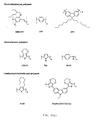
- Figure 2(a) shows the structure of exemplary electroluminescent polymers comprising MEH-PPV, PPP and PFO as well as exemplary electrochromic polymers comprising PEDOT, Ppy and PANI.
- One or more electroluminescent polymers can be used together with one or more electrochromic polymers to provide the desired electrochromic and electroluminescence required for electroactive layer 130, with the respective representative polymer structures performing the noted function well.
- electroactive layer 130 consists of a single material which provides both electroluminescence and an electrochromically active working electrode material. Exemplary materials which provide both electroluminescence and electrochromism are shown in Fig. 2(a) include P3OT and poly(bis-EDOT-Et-Cz).
- Figure 2(b) shows some additional exemplary compositions of materials which provide both electroluminescence and electrochromism for electrochromic/electroluminescent devices according to the invention.
- a first class of materials comprise metal complexes. Ru(bpy) 3 (PF 6 ) 2 tris(2,2'-bipyridyl)ruthenium[II] hexafluorophosphate and Ru(bec-bpy) 3 (PF 6 ) 2 tris[bis(ethoxycarbonyl)-2,2'-bipyridine] ruthenium[II] hexafluorophosphate are examples of this metal complex class shown in Fig. 2(b) which can be used alone or blended into an inert polymer matrix.
- a second class of materials are novel electroluminescent polymers.
- Figure 2(b) shows structures for poly(bis-OR8-phenylene-N-OR7-carbazole) and poly(OR9-thiphene-NOR7-carbazole) as examples of this class of polymers.
- a third class of materials comprise electroluminescent/electrochromic materials blended in a polymer matrix.
- Figure 2(b) shows Poly( alt -9-dihexyl-fluorene-N-ethyl-carbazole) which is blended in PMMA as well as MEH-PPV blended in PEO.
- Optically transparent electrode layer 140 can comprise materials including indium tin oxide (ITO), or fluorine doped tin oxide.
- ITO indium tin oxide
- fluorine doped tin oxide Alternatively, optically transparent electrically conducting polymers can be used, such as PEDOT/PSS.
- display device can include a pixel drive circuit as known in the art, such as disclosed in published U.S. Pat. Application No. 20030103021 to Young et al.
- the pixel drive circuit selects which pixels are in the on or off (EL mode), and which pixels are in a specific color state, including intermediate color states (EC mode).
- EL mode on or off
- EC mode intermediate color states
- a color state is used when the EL is off, and the EC polymer is initially neutral when the EL is turned on.
- the EC polymer can be colored or transmissive in EL mode. Since the EC state does not require a bias to retain its color, the EC state is an energy saving mode and is said to have "memory".
- counterelectrode layer 110 and electroactive layer 130 both include electrochemically active polymeric materials.
- Electroactive layer 130 can be a cathodically coloring or anodically coloring polymer. When electroactive layer 130 is a cathodically coloring polymer a negative bias is applied to layer 130 with respect to counter electrode 110 produces a colored state. When the electroactive layer includes an anodically coloring polymer, a positive bias applied to layer 130 with respect to counter electrode 110 produces a colored state.
- the cathodically coloring polymer can comprise a poly(3,4-alkylenedioxyheterocycle), such as alkylenedioxypyrrole, or alkylenedioxythiophene.
- the poly(3,4-alkylenedioxyheterocycle) can comprise a bridge-alkyl substituted poly(3,4-alkylenedioxythiophene), such as PProDOT-(methyl) 2 , PProDOT-(hexyl) 2 , or PProDOT-(ethylhexyl) 2 .
- the electrochemically active working electrode provided by electroactive layer 130 can be an anodically coloring polymer.
- a wide range of such materials are available, such as PPV or PPP derivatives.
- U.S. Patent No. 6,791,738 ('738) entitled ELECTROCHROMIC POLYMERS AND POLYMER ELECTROCHROMIC DEVICES describes some semiconducting electrochromic polymers including high band polymers having band gaps >3.0 eV.
- Named inventors for '738 include the inventor named in the present invention.
- Electrochemically active anodically coloring polymers disclosed prior to '738 are generally not optically clear and colorless in their transmissive states because the band gaps provided are not sufficiently high for the ⁇ - ⁇ * absorption to be excluded from the visible region, thus providing coloration to the transmissive state of the devices.
- band gaps of such polymers are generally no more than 2.7 eV.
- E hc/ ⁇ ; where h is Plank's constant and c is the speed of light).
- a high band gap polymer is not required for use with the invention, but can provide a highly transmissive state for the electroactive layer 130 allowing the reflective metal electrode 125 to be visible when desired for a given application.
- the EL material can be selected from a wide range of materials.
- the EL material can be MEH-PPV, PPP or PFO shown in Fig. 2(a) , or provided by a single material which provides EL and EC, such as shown in Fig. 2(b) .
- the invention is expected to have a wide range of applications since displays according to the invention can operate independent of ambient light. Any form of display in which one would want to have either emission of light or change of color on surface can benefit from the invention.
- Some exemplary applications include
- Electrochromic devices inherently operate with electrochromic memory since once the color change is set by an appropriate redox reaction, no current is required at that pixel. Thus, electrochromic operation uses less energy than emitting devices which require constant power consumption, thus allowing longer operating times for the power supply used in the system, typically a battery.
- the user Upon entering the dark tunnel, the user (or a light sensor based on some light level threshold) flips a switch to light emitting mode wherein the display will be visible in the dark.
- Light sensors known in the art can be based on a variety of devices including photodiodes photoresistors, photransistors, or CCDs.
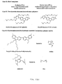
- Example 1 A device was constructed in order to make use of both the electrochromic and electroluminescent properties of certain metal complexes.
- Stock solutions of poly(methyl methacrylate) (PMMA), and the metal complex tris(2,2'-bipyridyl) ruthenium(II) hexafluorophosphate ([Ru(bpy) 3 ](PF 6 ) 2 ), ( Fig. 2(b) were prepared in acetonitrile with concentrations of 33 mg/mL and 53 mg/mL, respectively.
- PMMA serves as an inert matrix which provides good film forming properties. These solutions were blended in a 1:3 volumetric ratio.
- Composite films were spin cast from this solution onto an ITO coated glass at a rate of 2000 rpm to yield a thickness of 100 nm.
- the film on the glass ITO substrate was kept under vacuum at room temperature for 1 h and then heated under vacuum to 120 °C for 2 h.
- a porous gold membrane with a gold thickness of about 100 nm was then placed on the top of the film. A small amount of electrolyte was spread on the porous gold membrane. PEDOT, that was electrochemically deposited on gold. MYLAR® was placed at the very top facing towards the gold to serve as the counter electrode material 110. Connections to the two gold electrodes and the ITO electrode were made by copper bands. The porous gold membrane and the ITO were accessed as electrodes in order to run the device in light emitting electrochemical cell mode, while the ITO and the gold MYLAR® electrodes were utilized to run the device in electrochromic mode.
- Example 2 A device was constructed using MEH-PPV which as noted above is a material which provides both electrochromism and electroluminescence.
- MEH-PPV poly[2-methoxy-5-(2'-ethyl-hexyloxy)-1,4-phenylene vinylene]
- PEO poly(ethylene oxide)
- Li triflate lithium trifluoromethanesulfonate
- Composite polymer films were spin cast from this solution onto an ITO coated glass at a rate of 2000 rpm to yield a thickness of 200 nm. That film on the glass ITO substrate was heated under vacuum at 80 °C for 2 h.
- a porous gold membrane with a gold thickness of 100 nm was then placed on the top of the film. A small amount of electrolyte was spread on the porous gold membrane. PEDOT, that was electrochemically deposited on gold MYLAR® was placed at the very top facing towards the gold. Connections to the two gold electrodes and the ITO electrode were made by copper bands. The porous gold membrane and the ITO were accessed as electrodes in order to run the device in light emitting electrochemical cell mode, while the ITO and the gold MYLAR® electrodes were utilized to run the device in electrochromic mode.
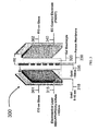
- FIG. 3 shows exemplary layers comprising a dual EL/EC device 300 according to the invention shown partially separated to facilitate description of fabrication steps to form the dual EL/EC.
- the device 300 will change color (EC mode) or emit light (EL mode). This is possible because both EL and EC operations require an electroactive layer 315 (MEH-PPV).
- the EL mode may use an ionic conductive material blended with the light emitting material.
- the EC mode uses an ionic transport layer 320 shown as a gel electrolyte.
- Electroactive layer 315 includes a thin gold layer 318 thereon.
- a porous membrane (substrate) 330 having gold 335 thereon as the middle electrode in this hybrid EL/EC device 300 ensures fast transfer of ions between the electrochemically active layers and electrical contact to the outside of the device. Moreover, when placed next to one another in the completed device thin gold layer 318 on the electroactive layer 315 together with gold layer 335 on the membrane 330 effectively provides a single layer of gold with a good electrical contact.
- the counter electrode shown as oxidized PXDOT 340 completes the active portion of device 300. Optically transparent ITO on glass layers 361 and 362 sandwich the active portion of device 300.
- a mixture of MEH-PPV, PEO (chemical structures shown in Fig. 2(b) ), and Li triflate (see below for respective chemical structure) were spun cast from dichloroethane on a clean ITO/Glass (1 inch X 1 inch) substrate to form the electroactive MEH-PPV layer 315.
- a thin layer of gold ( ⁇ 10 nm) 318 was then vapor deposited onto the MEH-PPV layer 315 through a mask at high vacuum ( ⁇ 4 x 10 -7 Torr).
- the middle contact was formed by depositing 100 nm gold 335 on a microporous membrane 330 (Pore size: about 10 ⁇ m).
- the middle contact was then pressed onto the MEH-PPV layer 315 to ensure electrical contact between the gold layers 318 and 335.
- a thin film of PXDOT (structure shown below) was separately deposited on an ITO/Glass substrate (electrochemically polymerized or solution cast) and was electrochemically oxidized to form the counter electrode 340.
- This counter electrode 340 was then placed on the middle contact (face down) separated by a thin layer of ionically conducting gel electrolyte 320.
- Photographs of the electrochromic operation of a patterned EL/EC device 300 (after pressing together) between the orange/red and transparent light blue states were recorded.
- +1V was applied between the working electrode 315 through middle contact 335 and the counter electrode 340 through ITO 362
- the MEH-PPV working electrode layer 315 became oxidized and PXDOT layer 340 was reduced which results in discoloration of the device to show the light blue of the MEH-PPV and the blue color of PXDOT layer 340 underneath. This switching was shown to be reversible by repeating this sequence multiple times.
- Figure 4(a) shows the current-voltage characteristics of this device when ⁇ 1V was applied for 10 seconds and the current was monitored against time. The switching time was determined to be about 3 seconds from the decay of the current. The maximum current values are about 0.1 mA which is typical for polymer based electrochromic devices.
- Figure 4(b) shows the reflectance spectra of this device at two extreme states ( ⁇ 1V) in the visible region. At -1V, the MEH-PPV layer is neutral with a reflectance minimum at about 510 nm. When the bias is switched to +1V, MEH-PPV is oxidized (bleached) to yield higher reflectance (lower absorption) values at 510 nm. This also results in coloring of the PEDOT layer underneath to yield lower reflectance values at wavelengths above 580 nm.
- the device When the device was biased for EL operation and -6V was applied between the MEH-PPV layer and the middle contact, the device lit up for a short period of time followed by complete oxidation (discoloration) of the MEH-PPV layer.
- Another EL/EC device was fabricated with the same configuration as described relative to Example 3, except without the presence of the gel electrolyte layer 320. As expected, this device did not show electrochromism as there was no ionically conducting medium to transfer charges between the MEH-PPV working electrode layer and the counter electrode. EL operation of this device yielded light emission (orange) from the patterned gold contacts as expected.
Claims (17)
- Kombinierte elektrochrome/elektrolumineszente Vorrichtung, die mindestens ein Pixel umfasst, wobei dieses Pixel umfasst:ein Substrat (107) mit einer elektrisch leitenden Oberfläche (105);eine elektrochemisch aktive Gegenelektrodenschicht (110), die auf der elektrisch leitenden Oberfläche angeordnet ist;eine Elektrolytschicht (115), die auf der Gegenelektrode angeordnete Elektrolyte vorsieht, eine elektrisch leitende Schicht (125), die auf dem Elektrolyt angeordnet ist,eine elektroaktive Schicht (130), die auf der elektrisch leitenden Schicht angeordnet ist, wobei die elektrisch leitende Schicht einen Transport der Elektrolyte hierdurch vorsieht, dadurch gekennzeichnet, dass die elektroaktive Schicht sowohl eine Elektrolumineszenz als auch eine elektrochemisch aktive Arbeits-Elektrode aufweist und eine optisch transparente Elektrodenschicht (140) auf der aktiven Schicht angeordnet ist.
- Vorrichtung nach Anspruch 1, wobei die elektrisch leitende Schicht umfasst:eine durchlässige Membrane (330);elektrisch leitendes Material (335), das auf einer Oberseite der Membran angeordnet ist, wobei ein Teil des elektrisch leitenden Materials in die Membran eindringt;mindestens einen rückseitigen Kontaktleiter, der auf einer Rückseite der Membran angeordnet ist, wobei das elektrisch leitende Material, das auf der Oberseite der Membran angeordnet ist, durch einen leitenden Kanal durch die Membran, der das elektrisch leitende Material umfasst, mit dem rückseitigen Kontaktleiter gekoppelt ist.
- Vorrichtung nach Anspruch 1, wobei die elektrisch leitende Schicht eine poröse Elektrode ist.
- Vorrichtung nach Anspruch 1, wobei die elektroaktive Schicht ein erstes Material umfasst, das eine Elektrolumineszenz bereitstellt, und ein zweites Material, das eine Elektrochromie bereitstellt.
- Vorrichtung nach Anspruch 1, wobei das mindestens eine Pixel eine Anordnung dieser Pixel umfasst.
- Vorrichtung nach Anspruch 1, wobei die elektroaktive Schicht ein einziges Material umfasst, welches sowohl Elektrolumineszenz als auch Elektrochromie bereitstellt,
- Vorrichtung nach Anspruch 6, wobei das einzige Material einen Metallkomplex umfasst.
- Vorrichtung nach Anspruch 6, wobei das einzige Material ein elektrolumineszentes/elektrochromes Polymer umfasst,
- Vorrichtung nach Anspruch 7, wobei der Metallkomplex in eine Polymermatrix eingefügt ist.
- Vorrichtung nach Anspruch 1, wobei die Arbeitselektrode ein sich kathodisch einfärbendes Polymer umfasst,
- Vorrichtung nach Anspruch 1, wobei die Arbeitselektrode ein sich anodisch einfärbendes Polymer umfasst.
- Vorrichtung nach Anspruch 1, wobei die Elektrolytschicht einen Gelelektrolyten umfasst.
- Vorrichtung nach Anspruch 1, wobei die Elektrolytschicht einen festen Elektrolyten umfasst.
- Vorrichtung nach Anspruch 13, wobei der feste Elektrolyt ein ionisch leitendes Polymer umfasst, das einen Komplex umfasst, wobei der Komplex mindestens ein Polymer mit mindestens einem darin gelösten Metallsalz beinhaltet.
- Vorrichtung nach Anspruch 14, wobei das Polymer mindestens eins ausgewählt aus der Gruppe bestehend aus Poly(Ethylenoxid), Poly(Propylenoxid), Methoxyethoxyethoxy substitutiertes Polyphosphazen und Polyurethane basierend auf Polyether umfasst.
- Vorrichtung nach Anspruch 1, weiterhin umfassend eine Energieversorgung, die zwischen der elektrisch leitenden Oberfläche und der elektrisch leitenden Schicht und zwischen der elektrisch leitenden Schicht und der optisch transparenten Elektrodenschicht angeschlossen ist.
- Vorrichtung nach Anspruch 1, wobei die elektroaktive Schicht Poly(bis-OR8-Phenylen-N-oR7-Carbazol) oder Poly(OR-Thiophen-N-OR7-Carbazol) umfasst.
Applications Claiming Priority (2)
| Application Number | Priority Date | Filing Date | Title |
|---|---|---|---|
| US62041204P | 2004-10-20 | 2004-10-20 | |
| PCT/US2005/037893 WO2006045043A1 (en) | 2004-10-20 | 2005-10-20 | Dual light emitting and electrochromic device |
Publications (2)
| Publication Number | Publication Date |
|---|---|
| EP1812821A1 EP1812821A1 (de) | 2007-08-01 |
| EP1812821B1 true EP1812821B1 (de) | 2008-08-27 |
Family
ID=35759092
Family Applications (1)
| Application Number | Title | Priority Date | Filing Date |
|---|---|---|---|
| EP05817277A Not-in-force EP1812821B1 (de) | 2004-10-20 | 2005-10-20 | Duale lichtemittierende und elektrochromische vorrichtung |
Country Status (7)
| Country | Link |
|---|---|
| US (1) | US7557499B2 (de) |
| EP (1) | EP1812821B1 (de) |
| JP (1) | JP2008517350A (de) |
| KR (1) | KR20070074566A (de) |
| AT (1) | ATE406595T1 (de) |
| DE (1) | DE602005009392D1 (de) |
| WO (1) | WO2006045043A1 (de) |
Families Citing this family (28)
| Publication number | Priority date | Publication date | Assignee | Title |
|---|---|---|---|---|
| US7450290B2 (en) * | 2001-06-25 | 2008-11-11 | University Of Washington | Electropolymerization of enhanced electrochromic (EC) polymer film |
| US7256923B2 (en) * | 2001-06-25 | 2007-08-14 | University Of Washington | Switchable window based on electrochromic polymers |
| US7826124B2 (en) * | 2001-06-25 | 2010-11-02 | University Of Washington Through Its Center For Commercialization | Flexible panel based on electrochromic polymers |
| US7808691B2 (en) * | 2002-06-25 | 2010-10-05 | University Of Washington | Green electrochromic materials |
| WO2008118967A1 (en) * | 2007-03-26 | 2008-10-02 | University Of Washington | Smart sunglasses, helmet faceshields and goggles based on electrochromic polymers |
| US7884994B2 (en) * | 2007-10-16 | 2011-02-08 | Saint Gobain Glass France | Electrochromic layers, device and process of producing same |
| CN101983356B (zh) * | 2008-03-24 | 2013-05-22 | 佛罗里达大学研究基金公司 | 双活化膜电致色显示装置 |
| WO2009129275A1 (en) * | 2008-04-15 | 2009-10-22 | University Of Florida Research Foundation, Inc. | Interdigitated electrode dual electroemissive/electrochromic devices |
| JP2010282128A (ja) * | 2009-06-08 | 2010-12-16 | Fuji Xerox Co Ltd | 表示媒体及び表示装置 |
| EP2545410A1 (de) | 2010-03-12 | 2013-01-16 | Battelle Memorial Institute | Elektrochrome vorrichtung zur steuerung von sichtbarer und infrarot-strahlung |
| CN103329035B (zh) * | 2010-12-28 | 2016-01-20 | 日东电工株式会社 | 多孔性电极片及其制造方法以及显示装置 |
| FR2994613B1 (fr) * | 2012-08-14 | 2014-09-05 | Commissariat Energie Atomique | Dispositif d'affichage electroluminescent et electrochrome, procede de fabrication associe |
| US9939706B2 (en) | 2013-03-26 | 2018-04-10 | Clearink Displays, Inc. | Displaced porous electrode for frustrating TIR and returning light through exit pupil |
| US9280029B2 (en) | 2013-05-13 | 2016-03-08 | Clearink Displays, Inc. | Registered reflective element for a brightness enhanced TIR display |
| KR20160013908A (ko) | 2013-05-22 | 2016-02-05 | 클리어잉크 디스플레이스 엘엘씨 | 향상된 컬러 필터 포화도를 위한 방법 및 장치 |
| EP3327498B1 (de) | 2013-07-08 | 2021-09-01 | Concord (Hk) International Education Limited | Tir-modulierte anzeige mit weitem betrachtungswinkel |
| US10705404B2 (en) | 2013-07-08 | 2020-07-07 | Concord (Hk) International Education Limited | TIR-modulated wide viewing angle display |
| US9740075B2 (en) | 2013-09-10 | 2017-08-22 | Clearink Displays, Inc. | Method and system for perforated reflective film display device |
| KR20180070711A (ko) | 2013-09-30 | 2018-06-26 | 클리어잉크 디스플레이스, 인코포레이티드 | 전면발광 반-역반사 디스플레이를 위한 방법 및 장치 |
| US9897890B2 (en) | 2014-10-07 | 2018-02-20 | Clearink Displays, Inc. | Reflective image display with threshold |
| JP6688291B2 (ja) | 2014-10-08 | 2020-04-28 | クリアインク ディスプレイズ, インコーポレイテッドClearink Displays, Inc. | カラーフィルタが位置合わせされた反射型ディスプレイ |
| KR102237211B1 (ko) * | 2015-02-23 | 2021-04-08 | 한국전자통신연구원 | 표시 패널, 그것을 포함하는 표시 장치 및 그것의 동작 방법 |
| KR102463735B1 (ko) * | 2015-06-22 | 2022-11-04 | 삼성디스플레이 주식회사 | 유기 발광 소자, 이의 제조 방법 및 이를 포함하는 유기 발광 표시 장치 |
| US10386691B2 (en) | 2015-06-24 | 2019-08-20 | CLEARink Display, Inc. | Method and apparatus for a dry particle totally internally reflective image display |
| US10261221B2 (en) | 2015-12-06 | 2019-04-16 | Clearink Displays, Inc. | Corner reflector reflective image display |
| US10386547B2 (en) | 2015-12-06 | 2019-08-20 | Clearink Displays, Inc. | Textured high refractive index surface for reflective image displays |
| KR102229145B1 (ko) * | 2016-01-29 | 2021-03-19 | 한국전자통신연구원 | 투명 디스플레이 장치 |
| CZ2022154A3 (cs) * | 2022-04-12 | 2023-06-07 | Marek Novák | Elektrochromický displej |
Family Cites Families (11)
| Publication number | Priority date | Publication date | Assignee | Title |
|---|---|---|---|---|
| JPH01172887A (ja) * | 1987-12-28 | 1989-07-07 | Tosoh Corp | Elパネル |
| US6754750B2 (en) * | 2001-05-17 | 2004-06-22 | Chaparral Network Storage Inc. | Method for automatically detecting and correcting duplicate controller SCSI ids |
| KR100921230B1 (ko) | 2001-11-21 | 2009-10-12 | 유니버시티 오브 플로리다 리서치 파운데이션, 아이엔씨. | 전색 중합체 및 중합체 전색 소자 |
| GB0129068D0 (en) * | 2001-12-05 | 2002-01-23 | Koninl Philips Electronics Nv | Display device |
| JP4259142B2 (ja) * | 2003-03-07 | 2009-04-30 | 株式会社デンソー | ディスプレイ装置 |
| TW583895B (en) * | 2003-03-31 | 2004-04-11 | Ritdisplay Corp | OEL device |
| JP4060779B2 (ja) * | 2003-10-21 | 2008-03-12 | 株式会社東芝 | 表示装置 |
| EP1687670B1 (de) * | 2003-11-19 | 2014-03-12 | University of Florida Research Foundation, Inc. | Verfahren zum kontaktieren strukturierter elektroden auf porösen substraten und einrichtungen dafür |
| JP4384005B2 (ja) * | 2004-10-15 | 2009-12-16 | 株式会社東芝 | 表示装置 |
| JP4568157B2 (ja) * | 2005-04-20 | 2010-10-27 | 株式会社東芝 | 表示装置 |
| US20070132371A1 (en) * | 2005-12-12 | 2007-06-14 | General Electric Company | Color tunable light-emitting devices and method of making the same |
-
2005
- 2005-10-20 EP EP05817277A patent/EP1812821B1/de not_active Not-in-force
- 2005-10-20 DE DE602005009392T patent/DE602005009392D1/de not_active Expired - Fee Related
- 2005-10-20 JP JP2007538063A patent/JP2008517350A/ja not_active Withdrawn
- 2005-10-20 AT AT05817277T patent/ATE406595T1/de not_active IP Right Cessation
- 2005-10-20 KR KR1020077008608A patent/KR20070074566A/ko not_active Application Discontinuation
- 2005-10-20 US US11/576,616 patent/US7557499B2/en not_active Expired - Fee Related
- 2005-10-20 WO PCT/US2005/037893 patent/WO2006045043A1/en active Application Filing
Also Published As
| Publication number | Publication date |
|---|---|
| US20080203910A1 (en) | 2008-08-28 |
| KR20070074566A (ko) | 2007-07-12 |
| JP2008517350A (ja) | 2008-05-22 |
| US7557499B2 (en) | 2009-07-07 |
| EP1812821A1 (de) | 2007-08-01 |
| DE602005009392D1 (de) | 2008-10-09 |
| WO2006045043A1 (en) | 2006-04-27 |
| ATE406595T1 (de) | 2008-09-15 |
Similar Documents
| Publication | Publication Date | Title |
|---|---|---|
| EP1812821B1 (de) | Duale lichtemittierende und elektrochromische vorrichtung | |
| KR100980353B1 (ko) | 다공성 기판상에 패턴화된 전극을 접촉시키는 방법 및 이에의한 소자 | |
| US8120245B2 (en) | Interdigitated electrode dual electroemissive/electrochromic devices | |
| Gazotti et al. | An all‐plastic and flexible electrochromic device based on elastomeric blends | |
| US7746533B2 (en) | Electrochromic devices utilizing very low band gap conjugated counter electrodes: preparation and use | |
| US7586663B1 (en) | Gel polymer electrolytes | |
| US7301687B2 (en) | Electrochemical device | |
| US6992808B2 (en) | Electrochromic display device and electrodeposition-type display device | |
| EP2196847B1 (de) | Elektrochrome anzeigevorrichtung und verfahren zu ihrer herstellung | |
| Seshadri et al. | Optimization, preparation, and electrical short evaluation for 30 cm2 active area dual conjugated polymer electrochromic windows | |
| Howard et al. | Optical properties of reversible electrodeposition electrochromic materials | |
| JP4244569B2 (ja) | エレクトロクロミック表示素子及びその製造方法、エレクトロクロミック表示装置 | |
| CN112666770B (zh) | 基于p(spma-mma)水凝胶电解质的电致变色柔性器件及其制备方法及应用 | |
| US20230063383A1 (en) | Electrochromic device and electrochromic method therefor | |
| CN212675329U (zh) | 一种电致变色器件以及显示装置 | |
| KR101570307B1 (ko) | 전기 화학 소자용 전극, 이의 제조방법 및 이를 포함하는 전기 화학 소자 | |
| EP0229438A1 (de) | Elektrochrome Vorrichtungen mit festen Elektrolyten | |
| JP2004258474A (ja) | フォトクロミック表示素子 | |
| JP2007121636A (ja) | エレクトロクロミック装置 |
Legal Events
| Date | Code | Title | Description |
|---|---|---|---|
| PUAI | Public reference made under article 153(3) epc to a published international application that has entered the european phase |
Free format text: ORIGINAL CODE: 0009012 |
|
| 17P | Request for examination filed |
Effective date: 20070518 |
|
| AK | Designated contracting states |
Kind code of ref document: A1 Designated state(s): AT BE BG CH CY CZ DE DK EE ES FI FR GB GR HU IE IS IT LI LT LU LV MC NL PL PT RO SE SI SK TR |
|
| DAX | Request for extension of the european patent (deleted) | ||
| GRAP | Despatch of communication of intention to grant a patent |
Free format text: ORIGINAL CODE: EPIDOSNIGR1 |
|
| RIC1 | Information provided on ipc code assigned before grant |
Ipc: G02F 1/15 20060101AFI20080212BHEP Ipc: H01L 27/32 20060101ALI20080212BHEP |
|
| GRAS | Grant fee paid |
Free format text: ORIGINAL CODE: EPIDOSNIGR3 |
|
| GRAA | (expected) grant |
Free format text: ORIGINAL CODE: 0009210 |
|
| AK | Designated contracting states |
Kind code of ref document: B1 Designated state(s): AT BE BG CH CY CZ DE DK EE ES FI FR GB GR HU IE IS IT LI LT LU LV MC NL PL PT RO SE SI SK TR |
|
| REG | Reference to a national code |
Ref country code: GB Ref legal event code: FG4D |
|
| REG | Reference to a national code |
Ref country code: CH Ref legal event code: EP |
|
| REG | Reference to a national code |
Ref country code: IE Ref legal event code: FG4D |
|
| REF | Corresponds to: |
Ref document number: 602005009392 Country of ref document: DE Date of ref document: 20081009 Kind code of ref document: P |
|
| REG | Reference to a national code |
Ref country code: CH Ref legal event code: NV Representative=s name: ING. MARCO ZARDI C/O M. ZARDI & CO. S.A. |
|
| PG25 | Lapsed in a contracting state [announced via postgrant information from national office to epo] |
Ref country code: IS Free format text: LAPSE BECAUSE OF FAILURE TO SUBMIT A TRANSLATION OF THE DESCRIPTION OR TO PAY THE FEE WITHIN THE PRESCRIBED TIME-LIMIT Effective date: 20081227 Ref country code: LT Free format text: LAPSE BECAUSE OF FAILURE TO SUBMIT A TRANSLATION OF THE DESCRIPTION OR TO PAY THE FEE WITHIN THE PRESCRIBED TIME-LIMIT Effective date: 20080827 |
|
| PG25 | Lapsed in a contracting state [announced via postgrant information from national office to epo] |
Ref country code: FI Free format text: LAPSE BECAUSE OF FAILURE TO SUBMIT A TRANSLATION OF THE DESCRIPTION OR TO PAY THE FEE WITHIN THE PRESCRIBED TIME-LIMIT Effective date: 20080827 Ref country code: LV Free format text: LAPSE BECAUSE OF FAILURE TO SUBMIT A TRANSLATION OF THE DESCRIPTION OR TO PAY THE FEE WITHIN THE PRESCRIBED TIME-LIMIT Effective date: 20080827 Ref country code: AT Free format text: LAPSE BECAUSE OF FAILURE TO SUBMIT A TRANSLATION OF THE DESCRIPTION OR TO PAY THE FEE WITHIN THE PRESCRIBED TIME-LIMIT Effective date: 20080827 Ref country code: ES Free format text: LAPSE BECAUSE OF FAILURE TO SUBMIT A TRANSLATION OF THE DESCRIPTION OR TO PAY THE FEE WITHIN THE PRESCRIBED TIME-LIMIT Effective date: 20081208 Ref country code: SI Free format text: LAPSE BECAUSE OF FAILURE TO SUBMIT A TRANSLATION OF THE DESCRIPTION OR TO PAY THE FEE WITHIN THE PRESCRIBED TIME-LIMIT Effective date: 20080827 |
|
| PG25 | Lapsed in a contracting state [announced via postgrant information from national office to epo] |
Ref country code: BE Free format text: LAPSE BECAUSE OF FAILURE TO SUBMIT A TRANSLATION OF THE DESCRIPTION OR TO PAY THE FEE WITHIN THE PRESCRIBED TIME-LIMIT Effective date: 20080827 |
|
| PG25 | Lapsed in a contracting state [announced via postgrant information from national office to epo] |
Ref country code: BG Free format text: LAPSE BECAUSE OF FAILURE TO SUBMIT A TRANSLATION OF THE DESCRIPTION OR TO PAY THE FEE WITHIN THE PRESCRIBED TIME-LIMIT Effective date: 20081127 Ref country code: DK Free format text: LAPSE BECAUSE OF FAILURE TO SUBMIT A TRANSLATION OF THE DESCRIPTION OR TO PAY THE FEE WITHIN THE PRESCRIBED TIME-LIMIT Effective date: 20080827 |
|
| PG25 | Lapsed in a contracting state [announced via postgrant information from national office to epo] |
Ref country code: SK Free format text: LAPSE BECAUSE OF FAILURE TO SUBMIT A TRANSLATION OF THE DESCRIPTION OR TO PAY THE FEE WITHIN THE PRESCRIBED TIME-LIMIT Effective date: 20080827 Ref country code: PT Free format text: LAPSE BECAUSE OF FAILURE TO SUBMIT A TRANSLATION OF THE DESCRIPTION OR TO PAY THE FEE WITHIN THE PRESCRIBED TIME-LIMIT Effective date: 20090127 Ref country code: RO Free format text: LAPSE BECAUSE OF FAILURE TO SUBMIT A TRANSLATION OF THE DESCRIPTION OR TO PAY THE FEE WITHIN THE PRESCRIBED TIME-LIMIT Effective date: 20080827 Ref country code: CZ Free format text: LAPSE BECAUSE OF FAILURE TO SUBMIT A TRANSLATION OF THE DESCRIPTION OR TO PAY THE FEE WITHIN THE PRESCRIBED TIME-LIMIT Effective date: 20080827 Ref country code: MC Free format text: LAPSE BECAUSE OF NON-PAYMENT OF DUE FEES Effective date: 20081031 |
|
| PLBE | No opposition filed within time limit |
Free format text: ORIGINAL CODE: 0009261 |
|
| STAA | Information on the status of an ep patent application or granted ep patent |
Free format text: STATUS: NO OPPOSITION FILED WITHIN TIME LIMIT |
|
| REG | Reference to a national code |
Ref country code: IE Ref legal event code: MM4A |
|
| PG25 | Lapsed in a contracting state [announced via postgrant information from national office to epo] |
Ref country code: EE Free format text: LAPSE BECAUSE OF FAILURE TO SUBMIT A TRANSLATION OF THE DESCRIPTION OR TO PAY THE FEE WITHIN THE PRESCRIBED TIME-LIMIT Effective date: 20080827 |
|
| 26N | No opposition filed |
Effective date: 20090528 |
|
| PG25 | Lapsed in a contracting state [announced via postgrant information from national office to epo] |
Ref country code: IT Free format text: LAPSE BECAUSE OF FAILURE TO SUBMIT A TRANSLATION OF THE DESCRIPTION OR TO PAY THE FEE WITHIN THE PRESCRIBED TIME-LIMIT Effective date: 20080827 Ref country code: DE Free format text: LAPSE BECAUSE OF NON-PAYMENT OF DUE FEES Effective date: 20090501 |
|
| PGFP | Annual fee paid to national office [announced via postgrant information from national office to epo] |
Ref country code: FR Payment date: 20090421 Year of fee payment: 4 Ref country code: NL Payment date: 20090427 Year of fee payment: 4 |
|
| PG25 | Lapsed in a contracting state [announced via postgrant information from national office to epo] |
Ref country code: IE Free format text: LAPSE BECAUSE OF NON-PAYMENT OF DUE FEES Effective date: 20081020 |
|
| PG25 | Lapsed in a contracting state [announced via postgrant information from national office to epo] |
Ref country code: SE Free format text: LAPSE BECAUSE OF FAILURE TO SUBMIT A TRANSLATION OF THE DESCRIPTION OR TO PAY THE FEE WITHIN THE PRESCRIBED TIME-LIMIT Effective date: 20081127 |
|
| REG | Reference to a national code |
Ref country code: NL Ref legal event code: V1 Effective date: 20100501 |
|
| PG25 | Lapsed in a contracting state [announced via postgrant information from national office to epo] |
Ref country code: PL Free format text: LAPSE BECAUSE OF FAILURE TO SUBMIT A TRANSLATION OF THE DESCRIPTION OR TO PAY THE FEE WITHIN THE PRESCRIBED TIME-LIMIT Effective date: 20080827 |
|
| REG | Reference to a national code |
Ref country code: CH Ref legal event code: PL |
|
| REG | Reference to a national code |
Ref country code: FR Ref legal event code: ST Effective date: 20100630 |
|
| PG25 | Lapsed in a contracting state [announced via postgrant information from national office to epo] |
Ref country code: NL Free format text: LAPSE BECAUSE OF NON-PAYMENT OF DUE FEES Effective date: 20100501 Ref country code: LU Free format text: LAPSE BECAUSE OF NON-PAYMENT OF DUE FEES Effective date: 20081020 Ref country code: CY Free format text: LAPSE BECAUSE OF FAILURE TO SUBMIT A TRANSLATION OF THE DESCRIPTION OR TO PAY THE FEE WITHIN THE PRESCRIBED TIME-LIMIT Effective date: 20080827 Ref country code: FR Free format text: LAPSE BECAUSE OF NON-PAYMENT OF DUE FEES Effective date: 20091102 Ref country code: HU Free format text: LAPSE BECAUSE OF FAILURE TO SUBMIT A TRANSLATION OF THE DESCRIPTION OR TO PAY THE FEE WITHIN THE PRESCRIBED TIME-LIMIT Effective date: 20090228 |
|
| PG25 | Lapsed in a contracting state [announced via postgrant information from national office to epo] |
Ref country code: TR Free format text: LAPSE BECAUSE OF FAILURE TO SUBMIT A TRANSLATION OF THE DESCRIPTION OR TO PAY THE FEE WITHIN THE PRESCRIBED TIME-LIMIT Effective date: 20080827 |
|
| PG25 | Lapsed in a contracting state [announced via postgrant information from national office to epo] |
Ref country code: CH Free format text: LAPSE BECAUSE OF NON-PAYMENT OF DUE FEES Effective date: 20091031 Ref country code: LI Free format text: LAPSE BECAUSE OF NON-PAYMENT OF DUE FEES Effective date: 20091031 Ref country code: GR Free format text: LAPSE BECAUSE OF FAILURE TO SUBMIT A TRANSLATION OF THE DESCRIPTION OR TO PAY THE FEE WITHIN THE PRESCRIBED TIME-LIMIT Effective date: 20081128 |
|
| PG25 | Lapsed in a contracting state [announced via postgrant information from national office to epo] |
Ref country code: GB Free format text: LAPSE BECAUSE OF NON-PAYMENT OF DUE FEES Effective date: 20091020 |