EP1806958A1 - Ceramic multilayer substrate and its producing method - Google Patents
Ceramic multilayer substrate and its producing method Download PDFInfo
- Publication number
- EP1806958A1 EP1806958A1 EP05799281A EP05799281A EP1806958A1 EP 1806958 A1 EP1806958 A1 EP 1806958A1 EP 05799281 A EP05799281 A EP 05799281A EP 05799281 A EP05799281 A EP 05799281A EP 1806958 A1 EP1806958 A1 EP 1806958A1
- Authority
- EP
- European Patent Office
- Prior art keywords
- ceramic
- chip electronic
- electronic component
- layers
- multilayer substrate
- Prior art date
- Legal status (The legal status is an assumption and is not a legal conclusion. Google has not performed a legal analysis and makes no representation as to the accuracy of the status listed.)
- Withdrawn
Links
Images


Classifications
-
- H—ELECTRICITY
- H05—ELECTRIC TECHNIQUES NOT OTHERWISE PROVIDED FOR
- H05K—PRINTED CIRCUITS; CASINGS OR CONSTRUCTIONAL DETAILS OF ELECTRIC APPARATUS; MANUFACTURE OF ASSEMBLAGES OF ELECTRICAL COMPONENTS
- H05K1/00—Printed circuits
- H05K1/18—Printed circuits structurally associated with non-printed electric components
- H05K1/182—Printed circuits structurally associated with non-printed electric components associated with components mounted in printed circuit boards [PCB], e.g. insert-mounted components [IMC]
- H05K1/185—Printed circuits structurally associated with non-printed electric components associated with components mounted in printed circuit boards [PCB], e.g. insert-mounted components [IMC] associated with components encapsulated in the insulating substrate of the PCBs; associated with components incorporated in internal layers of multilayer circuit boards
- H05K1/186—Printed circuits structurally associated with non-printed electric components associated with components mounted in printed circuit boards [PCB], e.g. insert-mounted components [IMC] associated with components encapsulated in the insulating substrate of the PCBs; associated with components incorporated in internal layers of multilayer circuit boards manufactured by mounting on or connecting to patterned circuits before or during embedding
-
- H—ELECTRICITY
- H05—ELECTRIC TECHNIQUES NOT OTHERWISE PROVIDED FOR
- H05K—PRINTED CIRCUITS; CASINGS OR CONSTRUCTIONAL DETAILS OF ELECTRIC APPARATUS; MANUFACTURE OF ASSEMBLAGES OF ELECTRICAL COMPONENTS
- H05K3/00—Apparatus or processes for manufacturing printed circuits
- H05K3/46—Manufacturing multilayer circuits
-
- B—PERFORMING OPERATIONS; TRANSPORTING
- B32—LAYERED PRODUCTS
- B32B—LAYERED PRODUCTS, i.e. PRODUCTS BUILT-UP OF STRATA OF FLAT OR NON-FLAT, e.g. CELLULAR OR HONEYCOMB, FORM
- B32B18/00—Layered products essentially comprising ceramics, e.g. refractory products
-
- C—CHEMISTRY; METALLURGY
- C04—CEMENTS; CONCRETE; ARTIFICIAL STONE; CERAMICS; REFRACTORIES
- C04B—LIME, MAGNESIA; SLAG; CEMENTS; COMPOSITIONS THEREOF, e.g. MORTARS, CONCRETE OR LIKE BUILDING MATERIALS; ARTIFICIAL STONE; CERAMICS; REFRACTORIES; TREATMENT OF NATURAL STONE
- C04B35/00—Shaped ceramic products characterised by their composition; Ceramics compositions; Processing powders of inorganic compounds preparatory to the manufacturing of ceramic products
- C04B35/622—Forming processes; Processing powders of inorganic compounds preparatory to the manufacturing of ceramic products
- C04B35/626—Preparing or treating the powders individually or as batches ; preparing or treating macroscopic reinforcing agents for ceramic products, e.g. fibres; mechanical aspects section B
- C04B35/63—Preparing or treating the powders individually or as batches ; preparing or treating macroscopic reinforcing agents for ceramic products, e.g. fibres; mechanical aspects section B using additives specially adapted for forming the products, e.g.. binder binders
- C04B35/632—Organic additives
-
- C—CHEMISTRY; METALLURGY
- C04—CEMENTS; CONCRETE; ARTIFICIAL STONE; CERAMICS; REFRACTORIES
- C04B—LIME, MAGNESIA; SLAG; CEMENTS; COMPOSITIONS THEREOF, e.g. MORTARS, CONCRETE OR LIKE BUILDING MATERIALS; ARTIFICIAL STONE; CERAMICS; REFRACTORIES; TREATMENT OF NATURAL STONE
- C04B35/00—Shaped ceramic products characterised by their composition; Ceramics compositions; Processing powders of inorganic compounds preparatory to the manufacturing of ceramic products
- C04B35/622—Forming processes; Processing powders of inorganic compounds preparatory to the manufacturing of ceramic products
- C04B35/626—Preparing or treating the powders individually or as batches ; preparing or treating macroscopic reinforcing agents for ceramic products, e.g. fibres; mechanical aspects section B
- C04B35/63—Preparing or treating the powders individually or as batches ; preparing or treating macroscopic reinforcing agents for ceramic products, e.g. fibres; mechanical aspects section B using additives specially adapted for forming the products, e.g.. binder binders
- C04B35/632—Organic additives
- C04B35/634—Polymers
-
- C—CHEMISTRY; METALLURGY
- C04—CEMENTS; CONCRETE; ARTIFICIAL STONE; CERAMICS; REFRACTORIES
- C04B—LIME, MAGNESIA; SLAG; CEMENTS; COMPOSITIONS THEREOF, e.g. MORTARS, CONCRETE OR LIKE BUILDING MATERIALS; ARTIFICIAL STONE; CERAMICS; REFRACTORIES; TREATMENT OF NATURAL STONE
- C04B35/00—Shaped ceramic products characterised by their composition; Ceramics compositions; Processing powders of inorganic compounds preparatory to the manufacturing of ceramic products
- C04B35/622—Forming processes; Processing powders of inorganic compounds preparatory to the manufacturing of ceramic products
- C04B35/626—Preparing or treating the powders individually or as batches ; preparing or treating macroscopic reinforcing agents for ceramic products, e.g. fibres; mechanical aspects section B
- C04B35/63—Preparing or treating the powders individually or as batches ; preparing or treating macroscopic reinforcing agents for ceramic products, e.g. fibres; mechanical aspects section B using additives specially adapted for forming the products, e.g.. binder binders
- C04B35/632—Organic additives
- C04B35/634—Polymers
- C04B35/63404—Polymers obtained by reactions only involving carbon-to-carbon unsaturated bonds
-
- C—CHEMISTRY; METALLURGY
- C04—CEMENTS; CONCRETE; ARTIFICIAL STONE; CERAMICS; REFRACTORIES
- C04B—LIME, MAGNESIA; SLAG; CEMENTS; COMPOSITIONS THEREOF, e.g. MORTARS, CONCRETE OR LIKE BUILDING MATERIALS; ARTIFICIAL STONE; CERAMICS; REFRACTORIES; TREATMENT OF NATURAL STONE
- C04B35/00—Shaped ceramic products characterised by their composition; Ceramics compositions; Processing powders of inorganic compounds preparatory to the manufacturing of ceramic products
- C04B35/622—Forming processes; Processing powders of inorganic compounds preparatory to the manufacturing of ceramic products
- C04B35/653—Processes involving a melting step
-
- C—CHEMISTRY; METALLURGY
- C04—CEMENTS; CONCRETE; ARTIFICIAL STONE; CERAMICS; REFRACTORIES
- C04B—LIME, MAGNESIA; SLAG; CEMENTS; COMPOSITIONS THEREOF, e.g. MORTARS, CONCRETE OR LIKE BUILDING MATERIALS; ARTIFICIAL STONE; CERAMICS; REFRACTORIES; TREATMENT OF NATURAL STONE
- C04B37/00—Joining burned ceramic articles with other burned ceramic articles or other articles by heating
- C04B37/008—Joining burned ceramic articles with other burned ceramic articles or other articles by heating by means of an interlayer consisting of an organic adhesive, e.g. phenol resin or pitch
-
- C—CHEMISTRY; METALLURGY
- C04—CEMENTS; CONCRETE; ARTIFICIAL STONE; CERAMICS; REFRACTORIES
- C04B—LIME, MAGNESIA; SLAG; CEMENTS; COMPOSITIONS THEREOF, e.g. MORTARS, CONCRETE OR LIKE BUILDING MATERIALS; ARTIFICIAL STONE; CERAMICS; REFRACTORIES; TREATMENT OF NATURAL STONE
- C04B37/00—Joining burned ceramic articles with other burned ceramic articles or other articles by heating
- C04B37/02—Joining burned ceramic articles with other burned ceramic articles or other articles by heating with metallic articles
- C04B37/023—Joining burned ceramic articles with other burned ceramic articles or other articles by heating with metallic articles characterised by the interlayer used
- C04B37/026—Joining burned ceramic articles with other burned ceramic articles or other articles by heating with metallic articles characterised by the interlayer used consisting of metals or metal salts
-
- C—CHEMISTRY; METALLURGY
- C04—CEMENTS; CONCRETE; ARTIFICIAL STONE; CERAMICS; REFRACTORIES
- C04B—LIME, MAGNESIA; SLAG; CEMENTS; COMPOSITIONS THEREOF, e.g. MORTARS, CONCRETE OR LIKE BUILDING MATERIALS; ARTIFICIAL STONE; CERAMICS; REFRACTORIES; TREATMENT OF NATURAL STONE
- C04B37/00—Joining burned ceramic articles with other burned ceramic articles or other articles by heating
- C04B37/02—Joining burned ceramic articles with other burned ceramic articles or other articles by heating with metallic articles
- C04B37/028—Joining burned ceramic articles with other burned ceramic articles or other articles by heating with metallic articles by means of an interlayer consisting of an organic adhesive, e.g. phenol resin or pitch
-
- C—CHEMISTRY; METALLURGY
- C04—CEMENTS; CONCRETE; ARTIFICIAL STONE; CERAMICS; REFRACTORIES
- C04B—LIME, MAGNESIA; SLAG; CEMENTS; COMPOSITIONS THEREOF, e.g. MORTARS, CONCRETE OR LIKE BUILDING MATERIALS; ARTIFICIAL STONE; CERAMICS; REFRACTORIES; TREATMENT OF NATURAL STONE
- C04B2235/00—Aspects relating to ceramic starting mixtures or sintered ceramic products
- C04B2235/65—Aspects relating to heat treatments of ceramic bodies such as green ceramics or pre-sintered ceramics, e.g. burning, sintering or melting processes
- C04B2235/656—Aspects relating to heat treatments of ceramic bodies such as green ceramics or pre-sintered ceramics, e.g. burning, sintering or melting processes characterised by specific heating conditions during heat treatment
-
- C—CHEMISTRY; METALLURGY
- C04—CEMENTS; CONCRETE; ARTIFICIAL STONE; CERAMICS; REFRACTORIES
- C04B—LIME, MAGNESIA; SLAG; CEMENTS; COMPOSITIONS THEREOF, e.g. MORTARS, CONCRETE OR LIKE BUILDING MATERIALS; ARTIFICIAL STONE; CERAMICS; REFRACTORIES; TREATMENT OF NATURAL STONE
- C04B2235/00—Aspects relating to ceramic starting mixtures or sintered ceramic products
- C04B2235/65—Aspects relating to heat treatments of ceramic bodies such as green ceramics or pre-sintered ceramics, e.g. burning, sintering or melting processes
- C04B2235/658—Atmosphere during thermal treatment
- C04B2235/6583—Oxygen containing atmosphere, e.g. with changing oxygen pressures
-
- C—CHEMISTRY; METALLURGY
- C04—CEMENTS; CONCRETE; ARTIFICIAL STONE; CERAMICS; REFRACTORIES
- C04B—LIME, MAGNESIA; SLAG; CEMENTS; COMPOSITIONS THEREOF, e.g. MORTARS, CONCRETE OR LIKE BUILDING MATERIALS; ARTIFICIAL STONE; CERAMICS; REFRACTORIES; TREATMENT OF NATURAL STONE
- C04B2237/00—Aspects relating to ceramic laminates or to joining of ceramic articles with other articles by heating
- C04B2237/02—Aspects relating to interlayers, e.g. used to join ceramic articles with other articles by heating
- C04B2237/12—Metallic interlayers
- C04B2237/121—Metallic interlayers based on aluminium
-
- C—CHEMISTRY; METALLURGY
- C04—CEMENTS; CONCRETE; ARTIFICIAL STONE; CERAMICS; REFRACTORIES
- C04B—LIME, MAGNESIA; SLAG; CEMENTS; COMPOSITIONS THEREOF, e.g. MORTARS, CONCRETE OR LIKE BUILDING MATERIALS; ARTIFICIAL STONE; CERAMICS; REFRACTORIES; TREATMENT OF NATURAL STONE
- C04B2237/00—Aspects relating to ceramic laminates or to joining of ceramic articles with other articles by heating
- C04B2237/02—Aspects relating to interlayers, e.g. used to join ceramic articles with other articles by heating
- C04B2237/12—Metallic interlayers
- C04B2237/124—Metallic interlayers based on copper
-
- C—CHEMISTRY; METALLURGY
- C04—CEMENTS; CONCRETE; ARTIFICIAL STONE; CERAMICS; REFRACTORIES
- C04B—LIME, MAGNESIA; SLAG; CEMENTS; COMPOSITIONS THEREOF, e.g. MORTARS, CONCRETE OR LIKE BUILDING MATERIALS; ARTIFICIAL STONE; CERAMICS; REFRACTORIES; TREATMENT OF NATURAL STONE
- C04B2237/00—Aspects relating to ceramic laminates or to joining of ceramic articles with other articles by heating
- C04B2237/30—Composition of layers of ceramic laminates or of ceramic or metallic articles to be joined by heating, e.g. Si substrates
- C04B2237/32—Ceramic
- C04B2237/34—Oxidic
- C04B2237/341—Silica or silicates
-
- C—CHEMISTRY; METALLURGY
- C04—CEMENTS; CONCRETE; ARTIFICIAL STONE; CERAMICS; REFRACTORIES
- C04B—LIME, MAGNESIA; SLAG; CEMENTS; COMPOSITIONS THEREOF, e.g. MORTARS, CONCRETE OR LIKE BUILDING MATERIALS; ARTIFICIAL STONE; CERAMICS; REFRACTORIES; TREATMENT OF NATURAL STONE
- C04B2237/00—Aspects relating to ceramic laminates or to joining of ceramic articles with other articles by heating
- C04B2237/30—Composition of layers of ceramic laminates or of ceramic or metallic articles to be joined by heating, e.g. Si substrates
- C04B2237/32—Ceramic
- C04B2237/34—Oxidic
- C04B2237/343—Alumina or aluminates
-
- C—CHEMISTRY; METALLURGY
- C04—CEMENTS; CONCRETE; ARTIFICIAL STONE; CERAMICS; REFRACTORIES
- C04B—LIME, MAGNESIA; SLAG; CEMENTS; COMPOSITIONS THEREOF, e.g. MORTARS, CONCRETE OR LIKE BUILDING MATERIALS; ARTIFICIAL STONE; CERAMICS; REFRACTORIES; TREATMENT OF NATURAL STONE
- C04B2237/00—Aspects relating to ceramic laminates or to joining of ceramic articles with other articles by heating
- C04B2237/30—Composition of layers of ceramic laminates or of ceramic or metallic articles to be joined by heating, e.g. Si substrates
- C04B2237/32—Ceramic
- C04B2237/36—Non-oxidic
- C04B2237/366—Aluminium nitride
-
- C—CHEMISTRY; METALLURGY
- C04—CEMENTS; CONCRETE; ARTIFICIAL STONE; CERAMICS; REFRACTORIES
- C04B—LIME, MAGNESIA; SLAG; CEMENTS; COMPOSITIONS THEREOF, e.g. MORTARS, CONCRETE OR LIKE BUILDING MATERIALS; ARTIFICIAL STONE; CERAMICS; REFRACTORIES; TREATMENT OF NATURAL STONE
- C04B2237/00—Aspects relating to ceramic laminates or to joining of ceramic articles with other articles by heating
- C04B2237/50—Processing aspects relating to ceramic laminates or to the joining of ceramic articles with other articles by heating
-
- C—CHEMISTRY; METALLURGY
- C04—CEMENTS; CONCRETE; ARTIFICIAL STONE; CERAMICS; REFRACTORIES
- C04B—LIME, MAGNESIA; SLAG; CEMENTS; COMPOSITIONS THEREOF, e.g. MORTARS, CONCRETE OR LIKE BUILDING MATERIALS; ARTIFICIAL STONE; CERAMICS; REFRACTORIES; TREATMENT OF NATURAL STONE
- C04B2237/00—Aspects relating to ceramic laminates or to joining of ceramic articles with other articles by heating
- C04B2237/50—Processing aspects relating to ceramic laminates or to the joining of ceramic articles with other articles by heating
- C04B2237/56—Using constraining layers before or during sintering
-
- C—CHEMISTRY; METALLURGY
- C04—CEMENTS; CONCRETE; ARTIFICIAL STONE; CERAMICS; REFRACTORIES
- C04B—LIME, MAGNESIA; SLAG; CEMENTS; COMPOSITIONS THEREOF, e.g. MORTARS, CONCRETE OR LIKE BUILDING MATERIALS; ARTIFICIAL STONE; CERAMICS; REFRACTORIES; TREATMENT OF NATURAL STONE
- C04B2237/00—Aspects relating to ceramic laminates or to joining of ceramic articles with other articles by heating
- C04B2237/50—Processing aspects relating to ceramic laminates or to the joining of ceramic articles with other articles by heating
- C04B2237/56—Using constraining layers before or during sintering
- C04B2237/562—Using constraining layers before or during sintering made of alumina or aluminates
-
- C—CHEMISTRY; METALLURGY
- C04—CEMENTS; CONCRETE; ARTIFICIAL STONE; CERAMICS; REFRACTORIES
- C04B—LIME, MAGNESIA; SLAG; CEMENTS; COMPOSITIONS THEREOF, e.g. MORTARS, CONCRETE OR LIKE BUILDING MATERIALS; ARTIFICIAL STONE; CERAMICS; REFRACTORIES; TREATMENT OF NATURAL STONE
- C04B2237/00—Aspects relating to ceramic laminates or to joining of ceramic articles with other articles by heating
- C04B2237/50—Processing aspects relating to ceramic laminates or to the joining of ceramic articles with other articles by heating
- C04B2237/68—Forming laminates or joining articles wherein at least one substrate contains at least two different parts of macro-size, e.g. one ceramic substrate layer containing an embedded conductor or electrode
-
- C—CHEMISTRY; METALLURGY
- C04—CEMENTS; CONCRETE; ARTIFICIAL STONE; CERAMICS; REFRACTORIES
- C04B—LIME, MAGNESIA; SLAG; CEMENTS; COMPOSITIONS THEREOF, e.g. MORTARS, CONCRETE OR LIKE BUILDING MATERIALS; ARTIFICIAL STONE; CERAMICS; REFRACTORIES; TREATMENT OF NATURAL STONE
- C04B2237/00—Aspects relating to ceramic laminates or to joining of ceramic articles with other articles by heating
- C04B2237/50—Processing aspects relating to ceramic laminates or to the joining of ceramic articles with other articles by heating
- C04B2237/70—Forming laminates or joined articles comprising layers of a specific, unusual thickness
- C04B2237/704—Forming laminates or joined articles comprising layers of a specific, unusual thickness of one or more of the ceramic layers or articles
-
- H—ELECTRICITY
- H05—ELECTRIC TECHNIQUES NOT OTHERWISE PROVIDED FOR
- H05K—PRINTED CIRCUITS; CASINGS OR CONSTRUCTIONAL DETAILS OF ELECTRIC APPARATUS; MANUFACTURE OF ASSEMBLAGES OF ELECTRICAL COMPONENTS
- H05K1/00—Printed circuits
- H05K1/02—Details
- H05K1/03—Use of materials for the substrate
- H05K1/0306—Inorganic insulating substrates, e.g. ceramic, glass
-
- H—ELECTRICITY
- H05—ELECTRIC TECHNIQUES NOT OTHERWISE PROVIDED FOR
- H05K—PRINTED CIRCUITS; CASINGS OR CONSTRUCTIONAL DETAILS OF ELECTRIC APPARATUS; MANUFACTURE OF ASSEMBLAGES OF ELECTRICAL COMPONENTS
- H05K2201/00—Indexing scheme relating to printed circuits covered by H05K1/00
- H05K2201/09—Shape and layout
- H05K2201/09009—Substrate related
- H05K2201/091—Locally and permanently deformed areas including dielectric material
-
- H—ELECTRICITY
- H05—ELECTRIC TECHNIQUES NOT OTHERWISE PROVIDED FOR
- H05K—PRINTED CIRCUITS; CASINGS OR CONSTRUCTIONAL DETAILS OF ELECTRIC APPARATUS; MANUFACTURE OF ASSEMBLAGES OF ELECTRICAL COMPONENTS
- H05K2201/00—Indexing scheme relating to printed circuits covered by H05K1/00
- H05K2201/10—Details of components or other objects attached to or integrated in a printed circuit board
- H05K2201/10613—Details of electrical connections of non-printed components, e.g. special leads
- H05K2201/10621—Components characterised by their electrical contacts
- H05K2201/10636—Leadless chip, e.g. chip capacitor or resistor
-
- H—ELECTRICITY
- H05—ELECTRIC TECHNIQUES NOT OTHERWISE PROVIDED FOR
- H05K—PRINTED CIRCUITS; CASINGS OR CONSTRUCTIONAL DETAILS OF ELECTRIC APPARATUS; MANUFACTURE OF ASSEMBLAGES OF ELECTRICAL COMPONENTS
- H05K2203/00—Indexing scheme relating to apparatus or processes for manufacturing printed circuits covered by H05K3/00
- H05K2203/30—Details of processes not otherwise provided for in H05K2203/01 - H05K2203/17
- H05K2203/308—Sacrificial means, e.g. for temporarily filling a space for making a via or a cavity or for making rigid-flexible PCBs
-
- H—ELECTRICITY
- H05—ELECTRIC TECHNIQUES NOT OTHERWISE PROVIDED FOR
- H05K—PRINTED CIRCUITS; CASINGS OR CONSTRUCTIONAL DETAILS OF ELECTRIC APPARATUS; MANUFACTURE OF ASSEMBLAGES OF ELECTRICAL COMPONENTS
- H05K3/00—Apparatus or processes for manufacturing printed circuits
- H05K3/46—Manufacturing multilayer circuits
- H05K3/4611—Manufacturing multilayer circuits by laminating two or more circuit boards
-
- H—ELECTRICITY
- H05—ELECTRIC TECHNIQUES NOT OTHERWISE PROVIDED FOR
- H05K—PRINTED CIRCUITS; CASINGS OR CONSTRUCTIONAL DETAILS OF ELECTRIC APPARATUS; MANUFACTURE OF ASSEMBLAGES OF ELECTRICAL COMPONENTS
- H05K3/00—Apparatus or processes for manufacturing printed circuits
- H05K3/46—Manufacturing multilayer circuits
- H05K3/4611—Manufacturing multilayer circuits by laminating two or more circuit boards
- H05K3/4626—Manufacturing multilayer circuits by laminating two or more circuit boards characterised by the insulating layers or materials
- H05K3/4629—Manufacturing multilayer circuits by laminating two or more circuit boards characterised by the insulating layers or materials laminating inorganic sheets comprising printed circuits, e.g. green ceramic sheets
-
- H—ELECTRICITY
- H10—SEMICONDUCTOR DEVICES; ELECTRIC SOLID-STATE DEVICES NOT OTHERWISE PROVIDED FOR
- H10W—GENERIC PACKAGES, INTERCONNECTIONS, CONNECTORS OR OTHER CONSTRUCTIONAL DETAILS OF DEVICES COVERED BY CLASS H10
- H10W70/00—Package substrates; Interposers; Redistribution layers [RDL]
- H10W70/60—Insulating or insulated package substrates; Interposers; Redistribution layers
- H10W70/62—Insulating or insulated package substrates; Interposers; Redistribution layers characterised by their interconnections
- H10W70/63—Vias, e.g. via plugs
-
- H—ELECTRICITY
- H10—SEMICONDUCTOR DEVICES; ELECTRIC SOLID-STATE DEVICES NOT OTHERWISE PROVIDED FOR
- H10W—GENERIC PACKAGES, INTERCONNECTIONS, CONNECTORS OR OTHER CONSTRUCTIONAL DETAILS OF DEVICES COVERED BY CLASS H10
- H10W90/00—Package configurations
- H10W90/701—Package configurations characterised by the relative positions of pads or connectors relative to package parts
- H10W90/721—Package configurations characterised by the relative positions of pads or connectors relative to package parts of bump connectors
- H10W90/724—Package configurations characterised by the relative positions of pads or connectors relative to package parts of bump connectors between a chip and a stacked insulating package substrate, interposer or RDL
-
- Y—GENERAL TAGGING OF NEW TECHNOLOGICAL DEVELOPMENTS; GENERAL TAGGING OF CROSS-SECTIONAL TECHNOLOGIES SPANNING OVER SEVERAL SECTIONS OF THE IPC; TECHNICAL SUBJECTS COVERED BY FORMER USPC CROSS-REFERENCE ART COLLECTIONS [XRACs] AND DIGESTS
- Y02—TECHNOLOGIES OR APPLICATIONS FOR MITIGATION OR ADAPTATION AGAINST CLIMATE CHANGE
- Y02P—CLIMATE CHANGE MITIGATION TECHNOLOGIES IN THE PRODUCTION OR PROCESSING OF GOODS
- Y02P70/00—Climate change mitigation technologies in the production process for final industrial or consumer products
- Y02P70/50—Manufacturing or production processes characterised by the final manufactured product
-
- Y—GENERAL TAGGING OF NEW TECHNOLOGICAL DEVELOPMENTS; GENERAL TAGGING OF CROSS-SECTIONAL TECHNOLOGIES SPANNING OVER SEVERAL SECTIONS OF THE IPC; TECHNICAL SUBJECTS COVERED BY FORMER USPC CROSS-REFERENCE ART COLLECTIONS [XRACs] AND DIGESTS
- Y10—TECHNICAL SUBJECTS COVERED BY FORMER USPC
- Y10T—TECHNICAL SUBJECTS COVERED BY FORMER US CLASSIFICATION
- Y10T428/00—Stock material or miscellaneous articles
- Y10T428/24—Structurally defined web or sheet [e.g., overall dimension, etc.]
- Y10T428/24802—Discontinuous or differential coating, impregnation or bond [e.g., artwork, printing, retouched photograph, etc.]
- Y10T428/24926—Discontinuous or differential coating, impregnation or bond [e.g., artwork, printing, retouched photograph, etc.] including ceramic, glass, porcelain or quartz layer
Definitions
- the present invention relates to ceramic multilayer substrates and methods for manufacturing the same, and more particularly to a ceramic multilayer substrate having a ceramic chip electronic component inside and a method for manufacturing the same.
- Patent Document 1 has disclosed an electronic component-embedding multilayer ceramic substrate and Patent Document 2 has disclosed a multilayer ceramic substrate and a method for manufacturing the same, as techniques for this field.
- the electronic component-embedding multilayer ceramic substrate disclosed in Patent Document 1 includes a multilayer ceramic substrate, a ceramic chip electronic component accommodated in a recess or a space defined by a through hole in the multilayer ceramic substrate, and conductors wiring the chip electronic component and disposed between layers or in spaces of the multilayer ceramic substrate. Since the chip electronic component is thus accommodated in a space of the multilayer ceramic substrate, the resulting multilayer ceramic substrate can have a desired shape, ensuring flatness.
- a capacitor element such as a capacitor element, an inductor element, and a resistor element
- functional elements are prepared in advance using plate-shaped sintered compact plates (corresponding to the ceramic chip electronic component) that are prepared by previously firing such ceramic functional elements, and these functional elements are embedded in a green multilayer composite.
- the green multilayer composite includes a green base layer, a constraining layer containing a sintering-resistant material, and wiring conductors. When the green multilayer composite is fired, the constraining layer acts to constrain the shrinkage of the green base layer in the main surface direction.
- Such a constrained sintering process using the constraining layer allows the green multilayer composite to be fired with the embedded ceramic functional elements without problems, and besides prevents mutual diffusion between the constituents of the ceramic functional elements and the green base layer.
- the functional elements can maintain their properties even after firing.
- the multilayer ceramic substrates disclosed in Patent Documents 1 and 2 are manufactured by firing a stack of ceramic green sheets having a ceramic chip electronic component inside. Consequently, the ceramic chip electronic component embedded in the fired multilayer ceramic substrate may be cracked, or broken in some cases. This occurred in the constrained sintering process using a constraining layer.
- the multilayer ceramic substrate is fired with the ceramic chip electronic component in close contact with the ceramic green sheets, it is difficult to prevent the mutual diffusion between the constituents of the ceramic chip electronic component and ceramic layers. Even the technique disclosed in Patent Document 2 may degrade the properties of the resulting chip electronic component.
- the strength of the substrate may be significantly degraded around the cavity.
- an object of the invention is to provide a highly reliable ceramic multilayer substrate containing a ceramic chip electronic component with no damage such as cracks whose properties are not degraded, and to provide a method for manufacturing the same.
- the inventers of the present invention have studied the cause of the damage to the ceramic chip electronic component embedded in a ceramic multilayer substrate.
- the inventors was found that when the ceramic layers of the ceramic multilayer substrate have a thermal expansion coefficient largely different from that of the ceramic chip electronic component, the ceramic chip electronic component is likely to crack or break. If the shrinkage of the substrate in its surface direction is reduced by employing a constrained sintering process, a non-shrinking ceramic chip electronic component can be embedded.
- ceramic chip electronic components such as monolithic ceramic capacitors, are often constituted of a high-dielectric constant material and high-dielectric constant materials generally have high thermal expansion coefficients.
- the green ceramic layer is often formed of a low-dielectric constant material and low-dielectric constant materials generally have low thermal expansion coefficients.
- the ceramic chip electronic component and the green ceramic layers in close contact with each other are fired together and then cooled to room temperature, the ceramic chip electronic component is shrunken much more than the ceramic layers during cooling, and consequently a tension from the ceramic layers is placed on the ceramic chip electronic component.
- the ceramic chip electronic component is made of a ceramic material. Since ceramic materials are less resistant to tensile stress, the ceramic chip electronic component is cracked or broken by the tension from the ceramic layers. Accordingly, the material of the ceramic chip electronic component embedded in the ceramic multilayer substrate is limited. In other words, the disadvantages that the ceramic chip electronic component is damaged and that the material of the ceramic chip electronic component is limited can be eliminated, unless the ceramic chip electronic component and the ceramic layers are in close contact with each other.
- a method for manufacturing a ceramic multilayer substrate as set forth in Claim 1 manufactures a ceramic multilayer substrate by simultaneously firing a green ceramic stack prepared by stacking a plurality of green ceramic layers and a ceramic chip electronic component including a terminal electrode and an elementary body made of a ceramic sintered compact and disposed inside the green ceramic stack.
- a contact inhibitor is disposed between the ceramic chip electronic component and the green ceramic stack, and the green ceramic stack, the ceramic chip electronic component, and the contact inhibitor are fired together.
- Claim 2 provides the method for manufacturing the ceramic multilayer substrate according to Claim 1, in which the contact inhibitor is disposed on the surface of the ceramic sintered compact.
- Claim 3 provides the method for manufacturing the ceramic multilayer substrate according to Claim 1 or 2, in which the contact inhibitor is a resin that can burn or decompose at a temperature lower than or equal to the sintering temperature of the green ceramic layers.
- Claim 4 provides the method for manufacturing the ceramic multilayer substrate according to Claim 1 or 2, in which the contact inhibitor is a ceramic powder that is not substantially sintered at the sintering temperature of the green ceramic layers.
- Claim 5 provides the method for manufacturing the ceramic multilayer substrate according to any one of Claims 1 to 4, in which the green ceramic layers are formed of a low-temperature co-fired ceramic material, and a conductor pattern mainly containing silver or copper is formed inside the green ceramic stack.
- Claim 6 provides the method for manufacturing the ceramic multilayer substrate according to any one of Claims 1 to 5, further including the step of disposing a shrinkage retardant layer made of a sintering-resistant powder not substantially sintered at the sintering temperature of the green ceramic layers on either or both main surfaces of the green ceramic stack.
- a ceramic multilayer substrate as set forth in Claim 7 includes: a ceramic stack including a plurality of ceramic layers stacked and a conductor pattern; and a ceramic chip electronic component disposed at the interface between any two adjacent layers of the ceramic layers.
- the ceramic chip electronic component includes a terminal electrode and an elementary body made of a ceramic sintered compact. The elementary body is disposed with a gap at the interface between the elementary body and the ceramic stack.
- a ceramic multilayer substrate as set forth in Claim 8 includes a ceramic stack including a plurality of ceramic layers stacked and a conductor pattern; and a ceramic chip electronic component disposed at the interface between any two adjacent layers of the ceramic layers.
- the ceramic chip electronic component includes a terminal electrode and an elementary body made of a ceramic sintered compact. The elementary body is disposed with a green ceramic powder at the interface between the elementary body and the ceramic stack.
- Claim 9 provides the ceramic multilayer substrate according to Claim 7 or 8, in which the ceramic layers are low-temperature co-fired ceramic layers.
- the invention defined in Claims 1 to 9 can provide a highly reliable ceramic multilayer substrate containing a ceramic chip electronic component with no damage, such as cracks, whose properties are not degraded, and a method for manufacturing the ceramic multilayer substrate.
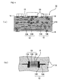
- a ceramic multilayer substrate 10 includes a ceramic stack 11 including a plurality of ceramic layers 11A stacked and an internal conductor pattern 12, and a plurality of ceramic chip electronic components 13 disposed at the interface between any two adjacent upper and lower ceramic layers 11A, as shown in Fig. 1(a).
- Each ceramic chip electronic component 13 includes an elementary body made of a ceramic sintered compact, and external terminal electrodes 13A at both ends of the elementary body.
- Surface electrodes 14 are disposed on both main surfaces of the ceramic stack 11 (upper and lower surfaces) .
- a plurality of surface mount components 20 are mounted on one main surface (upper surface in the present embodiment) of the ceramic stack 11 with the surface electrodes 14 formed between the surface mount components 20 and the ceramic stack 11.
- the surface mount components 20 include semiconductor elements, active elements such as gallium arsenide semiconductor elements, and passive elements such as capacitors, inductors, and resistors. These surface mount components are electrically connected to the surface electrodes 14 on the upper surface of the ceramic stack 11 through solder, electroconductive resin, or bonding wirers made of Au, A1, Cu and the like.
- the surface mount components 20 are electrically connected to the ceramic chip electronic components 13 with the surface electrodes 14 and the internal conductor pattern 12.
- the ceramic multilayer substrate 10 can be mounted on a mounting substrate, such as a mother board, using surface electrodes 14 on the other main surface (lower surface in the present embodiment).
- the material of the ceramic layers 11A of the ceramic stack 11 is not particularly limited as long as it is a ceramic material, for example, a low-temperature co-fired ceramic (LTCC) material is preferred.
- LTCC low-temperature co-fired ceramic
- Low-temperature co-fired ceramic materials can be sintered at temperatures of 1050°C or less and can also be fired simultaneously with silver, copper, or other metal having a low specific resistance.
- Exemplary low-temperature co-fired ceramics include glass-mixed LTCC materials prepared by mixing borosilicate glass with a ceramic powder such as alumina or forsterite, crystallized glass LTCC materials containing ZnO-MgO-Al 2 O 3 -SiO 2 crystallized glass, and non-glass LTCC materials containing BaO-Al 2 O 3 -SiO 2 ceramic powder or Al 2 O 3 -CaO-SiO 2 -MgO-B 2 O 3 ceramic powder.
- a ceramic powder such as alumina or forsterite
- crystallized glass LTCC materials containing ZnO-MgO-Al 2 O 3 -SiO 2 crystallized glass
- non-glass LTCC materials containing BaO-Al 2 O 3 -SiO 2 ceramic powder or Al 2 O 3 -CaO-SiO 2 -MgO-B 2 O 3 ceramic powder.
- the use of a low-temperature co-fired ceramic material as the material of the ceramic stack 11 allows the internal conductor pattern 12 and the surface electrodes 14 to be formed of a low-resistance, low-melting point metal, such as Ag or Cu. Consequently, the ceramic stack 11 and the internal conductor pattern 12 can be simultaneously fired at a low temperature of 1050°C or less.
- a high-temperature co-fired ceramic (HTCC) material may be used as the ceramic material.
- the high-temperature co-fired ceramic material may be prepared by sintering alumina, aluminium nitride, mullite, or the like containing a sintering agent, such as glass, at 1100°C or more.
- the internal conductor pattern 12 and the surface electrodes 14 are made of a metal selected from the group consisting of molybdenum, platinum, palladium, tungsten, nickel, and their alloys.
- the ceramic stack 11 includes the internal conductor pattern 12 formed inside and the surface electrodes 14 formed on both the upper and the lower surface, as shown in Fig. 1(a).
- the internal conductor pattern 12 includes in-plane conductors 12A formed in a predetermined pattern along the interface between any two adjacent upper and lower ceramic layers 11A and via conductors 12B formed in a predetermined pattern so as to connect some of the in-plane conductors 12A in the vertical direction.
- the ceramic chip electronic components 13 are disposed at the interface between any two adjacent upper and lower ceramic layers 11A, and their external terminal electrodes 13A are connected to the in-plane conductors 12A formed at the interface between those two upper and lower ceramic layers 11A, as shown in Figs. 1(a) and 1(b).
- the connection portion 12C of the in-plane conductor 12A to the external terminal electrode 13A is pressed into the ceramic layer 11A together with the ceramic chip electronic component 13 in such a manner that its section forms a substantially L-shape from the lower half of the end surface of the external terminal electrode 13A to the bottom surface.
- a gap V is formed between the ceramic layers 11A and the ceramic chip electronic component 13 except the external terminal electrodes 13A, that is, the elementary ceramic body 13B.
- the elementary ceramic body 13B is separate from the ceramic layers 11A.
- the gap V is formed using a contact inhibitor in a firing step, as described below. The gap prevents damage to the ceramic chip electronic component 13 during firing, resulting from the difference in thermal expansion coefficient between the ceramic chip electronic component 13 and the ceramic layers 11, and also prevents the mutual diffusion between the constituents of the elementary ceramic body 13B and the ceramic layers.
- the type of ceramic chip electronic component 13 is not particularly limited, and may use a ceramic sintered compact of barium titanate, ferrite, or the like fired at a temperature of 1050°C or more, and further 1200°C or more, as the elementary body.
- Exemplary ceramic chip electronic components include monolithic ceramic capacitors as shown in Fig. 1(b), inductors, filters, baluns, and couplers. A single or a plurality of ceramic chip electronic components can be appropriately selected from these components according to the application.
- the ceramic chip electronic component 13 used in the present embodiment includes an elementary ceramic body 13B including a plurality of ceramic layers stacked and a plurality of internal electrodes 13C each extending from one of the external terminal electrodes 13A toward the other external terminal electrode 13A, the external electrodes 13A face each other, as shown in the figure.
- Each ceramic layer of the elementary ceramic body 13B and the internal electrodes 13C overlying and underlying the ceramic layer define a capacitor.
- the plurality of ceramic chip electronic components 13 are disposed inside the ceramic stack 11.
- the plurality of ceramic chip electronic components 13 are the same type, including substantially the same number of ceramic layers made of substantially the same material with substantially the same thickness, and are disposed on the same ceramic layer 11A at the same depth from the upper surface of the ceramic stack 11, as shown in Fig. 1(a). Since the plurality of ceramic chip electronic components 13 are disposed at the same interface, a larger pressure or larger contraction force placed on the ceramic chip electronic components 13 during firing can act on each ceramic chip electronic component 13 substantially uniformly. Consequently, the variation in property among the plurality of ceramic chip electronic components 13 can be reduced.
- each ceramic chip electronic component 13 the ceramic layers of the elementary ceramic body 13B and the internal electrodes 13C are disposed parallel to the interfaces of the ceramic layers 11A, as shown in Fig. 1(b). Since the ceramic layers of the elementary ceramic body 13B are parallel to the ceramic layers 11A, a pressure or contraction force in the direction perpendicular to the interface of the ceramic layers 11A, if the pressure or the contraction force is applied, it acts on the ceramic chip electronic component 13 in the direction perpendicular to the direction of its cleavage. Consequently, cracks can be prevented in the ceramic chip electronic component 13.
- the thickness A and the length in the longitudinal direction of the ceramic chip electronic component 13 are defined as A and B respectively, it is preferable that the thickness A and the length B satisfy the relationship 2 ⁇ (B/A) ⁇ 40. If B/A is less than 2, the thickness of the ceramic chip electronic component 13 is relatively large. Accordingly the ceramic chip electronic component becomes liable to be affected by piezoelectric effect resulting from compression and thus the properties vary easily. If B/A increases to more than 40, the thickness of the ceramic chip electronic component 13 is reduced and the mechanical strength is reduced accordingly. Consequently, the ceramic chip electronic component becomes liable to be broken by a pressure when it is pressed.
- the thickness of the ceramic chip electronic component refers to the thickness in the direction in which the ceramic layers are stacked.
- the plurality of ceramic chip electronic components 13 be disposed on the same ceramic layer 11A, they may be located in any positions of the interface of the upper and lower ceramic layers as required. Sets of a plurality of ceramic chip electronic components 13 may be disposed at a plurality of interfaces different in vertical position. The ceramic chip electronic components 13 in each set are connected in series and/or in parallel using the connection portions 12C of the in-plane conductors 12A according to the application. Thus, a multifunctional, high-performance ceramic multilayer substrate 10 can be achieved.
- the surface mount components 20 are appropriately used in combination with the ceramic chip electronic components 13, as shown in Fig. 1(a).
- the ceramic chip electronic components 13 and the surface mount components 20 are electrically connected to each other through the surface electrodes 14 and the internal conductor pattern 12. If a component liable to be affected by power supply noises, such as an integrated circuit, is used as a surface mount component 20, a monolithic ceramic capacitor may be connected as the ceramic chip electronic component 13 right under the power terminal and the grounding terminal.
- noises can be efficiently removed so that, for example, power can be stably supplied and the output oscillation can be prevented, without limiting the arrangement of the terminals of the surface mount components 20, such as integrated circuits, or mounting a ceramic chip electronic component (for example, a monolithic ceramic capacitor) on another mother board.
- Figs. 2 to 4 a method for manufacturing the ceramic multilayer substrate 10 will be described.
- the ceramic multilayer substrate 10 is produced by a constrained sintering process.
- the constrained sintering process is a method in which the size of a ceramic stack 11 using a ceramic material is not substantially varied in its surface direction even after sintering the ceramic stack.
- a predetermined number of ceramic green sheets are formed of a slurry containing, for example, a low-temperature co-fired ceramic material.
- the ceramic green sheets 111A on which the ceramic chip electronic components 113 including the elementary bodies made of a ceramic sintered compact are disposed, via holes are formed in a predetermined pattern, as shown in Figs. 2(a) and 2(b).
- the via holes are filled with an electroconductive paste mainly containing, for example, Ag or Cu, to form via conductors 112B.
- the same electroconductive paste is applied onto the ceramic green sheet 111A in a predetermined pattern to form in-plane conductors 112A.
- the in-plane conductors 112A and the via conductors 112B are appropriately connected.
- the other ceramic green sheets 111A are formed in the same manner.
- the ceramic chip electronic components before firing are designated by reference numeral "113" and those after firing and cooling are designated by reference numeral "13".
- Ceramic chip electronic components 113 each including an elementary body made of a ceramic sintered compact, as shown in Fig. 2(C), is prepared.
- a resin paste prepared from a thermally decomposable resin is applied as a contact inhibitor over the entire surfaces of the elementary ceramic body 113B of the ceramic chip electronic component 113 except the external terminal electrodes 113A, and thus a paste layer 115 is formed to a thickness of 1 to 30 ⁇ m.
- the contact inhibitor is preferably formed over the entire surfaces of the elementary ceramic body 113B, and the contact inhibitor has to be formed on at least part of the surfaces, especially, it is preferably formed at the upper and lower surface, which added large pressure.
- any material can be used as the contact inhibitor as long as it can prevent mutually diffusing of the constituents between the ceramic chip electronic component 113 and the ceramic green sheet 111A during firing, and it can form a non-constraining region where the ceramic chip electronic component 113 can shrink after firing.
- a contact inhibitor may be a resin that can be burned or decomposed to form a gap V by firing, as in the present embodiment, or a ceramic powder that does not sinter to adhere to the elementary ceramic body 13B by firing.
- Burnable resins include, for example, butyral resins.
- Decomposable resins include, for example, acrylic resins.
- the ceramic powder can be, for example, below-described sintering-resistant powder.
- the resin paste may contain a low-temperature co-fired ceramic material to the extent that the formation of the gap is not hindered.
- an organic adhesive is applied or sprayed using a spray or the like onto the in-plane conductors 112A of the ceramic green sheet 111A on which the ceramic chip electronic components 113 are to be disposed, thus forming an organic adhesive layer (not shown). Then, the ceramic chip electronic components 113 are disposed on the ceramic green sheet 111A in a state where the external terminal electrodes 113A of the ceramic chip electronic components 113 are aligned with the in-plane conductors 112A of the ceramic green sheet 111A as shown in Fig. 2(b).
- the external terminal electrodes 113A of each ceramic chip electronic component 113 are bonded and fixed to the in-plane conductors 112A through the organic adhesive layer.
- the organic adhesive can be a mixture of a synthetic rubber or synthetic resin and a plasticizer.
- the thickness of the organic adhesive layer is preferably 3 ⁇ m or less when it is formed by coating, or 1 ⁇ m or less when it is formed by spraying.
- the ceramic green sheets 111A having the in-plane conductors 112A and the via conductors 112B and the ceramic green sheet 111A, on which the ceramic chip electronic components 113 are disposed, are stacked on a constraining layer 116 in a predetermined order, as shown in Fig. 3.
- the uppermost ceramic green sheet 111A having the surface electrodes 114 is placed on top of the stack.
- a green ceramic stack 111 is formed on the constraining layer 116.
- another constraining layer 116 is stacked on the upper surface of the green ceramic stack 111.
- the green ceramic stack 111 is thermocompression-bonded at a predetermined pressure from the upper and lower constraining layers 116 at a predetermined temperature to prepare a compressed body 110 shown in Fig.
- the constraining layer 116 is a sheet formed of a sintering-resistant powder (ceramic powder having a high sintering temperature, such as Al 2 O 3 ) not sintered at the sintering temperature of the green ceramic stack 111, for example, a slurry containing Al 2 O 3 as the main constituent and an organic binder as an accessory constituent.
- a sintering-resistant powder ceramic powder having a high sintering temperature, such as Al 2 O 3
- the firing temperature is preferably a temperature at which the low-temperature co-fired ceramic material can be sintered, and for example, it is in the range of 800 to 1050°C. Firing at a temperature of less than 800°C may not sufficiently sinter the ceramic components of the green ceramic stack 111. Firing at a temperature of more than 1050°C may melt the metal particles of the internal conductor pattern 12 to diffuse the metal in the green ceramic stack 111.
- the paste layer 115 formed over the external surfaces of the elementary ceramic body 113B of the ceramic chip electronic component 113 is burned or decomposed, so that narrow gaps V are formed between the elementary ceramic body 113B of each ceramic chip electronic component 113 and the ceramic green sheets 111A, as shown in Fig. 1(b). Consequently, the constituents of the ceramic layers 11A and the elementary ceramic body 113B of the ceramic chip electronic component 113 can be certainly prevented from mutually diffusing when the ceramic green sheets 111A are sintered. Thus, the properties of the ceramic chip electronic component 13 are not degraded after firing.
- the metal particles of the external terminal electrodes 113A of the ceramic chip electronic component 113 and the in-plane conductors 112A are grown to be integrated during sintering, and thus the external terminal electrodes 113A and the in-plane conductors 112A are connected to each other.
- the ceramic chip electronic component 113 is tightly connected to and integrated with the in-plane conductors 112A with the external terminal electrodes 113A by firing. Also, the gap V is formed between each ceramic chip electronic component and the ceramic green sheets 111A by burning or decomposition of the paste layer 115. Consequently, even if the ceramic chip electronic component 13 and the ceramic layers 11A have a large difference in thermal expansion coefficient during cooling after firing, the ductile in-plane conductors 12A can elongate accompanying the shrinkage of the ceramic chip electronic component 13. Thus, the ceramic chip electronic component 13 does not suffer from a strain, and cracks in or other damage to the ceramic chip electronic component 13 can be prevented.
- the external terminal electrodes 113A of the ceramic chip electronic component 113 may be an electroconductive paste that has been applied and baked, or an electroconductive paste that has been applied and dried, but not yet baked.
- a ceramic multilayer substrate 10 which having ceramic chip electronic components 13 inside, is produced by simultaneously firing a green ceramic stack 111 and ceramic chip electronic components 113, as described above.
- the green ceramic stack 111 is prepared by stacking a plurality of ceramic green sheets 111A.
- Each ceramic chip electronic component includes an elementary body made of a ceramic sintered compact, and external terminal electrodes 113A disposed at both ends of the elementary body.
- the ceramic chip electronic components are disposed inside the green ceramic stack 111.
- a paste layer 115 is previously formed on the entire surfaces of the elementary ceramic body 113B, and the ceramic chip electronic components 113, each having the paste layer 115, are disposed at the interface of any adjacent two upper and lower ceramic green sheets 111A.
- the ceramic green sheets 111A, the ceramic chip electronic components 113, and the paste layers 115 are fired with each paste layer 115 disposed between the ceramic green sheets 111A and the elementary ceramic body 113B of the ceramic chip electronic component 113.
- the paste layer 115 is burned or decomposed by firing, thus forming a gap V between the elementary ceramic body 113B of the ceramic chip electronic component 113 and the ceramic green sheets 111A. Consequently, the constituents of the elementary ceramic body 113B of the ceramic chip electronic component 113 and the ceramic layers 11A are prevented from mutually diffusing, so that the properties of the ceramic chip electronic component 13 are not degraded.
- the gap V between the ceramic chip electronic component 13 and the ceramic layers 11A allows the ceramic layers 11A to shrink through the ductile in-plane conductors 12A in between without constraint during cooling after firing.
- the ceramic chip electronic component 13 does not suffer from a strain, and cracks in or other damage to the ceramic chip electronic component 13 can be prevented.
- the present embodiment can provide a highly reliable ceramic multilayer substrate 10 containing ceramic chip electronic components 13 with no damage, such as cracks whose properties are not degraded.
- the ceramic layers 11A are low-temperature co-fired ceramic layers. Accordingly, a low-resistance and inexpensive metal, such as Ag or Cu, can be used for the internal conductor pattern 12 and the surface electrodes 14, thus reducing the manufacturing cost and increasing the high-frequency characteristics.
- a low-resistance and inexpensive metal such as Ag or Cu
- a ceramic multilayer substrate 10A of the present embodiment includes a ceramic stack 11, internal conductor patterns 12, and ceramic chip electronic components 13, and a plurality of surface mount components 20 are disposed on the upper surface of the ceramic stack 11, as shown in, for example, Figs. 5(a) and 5(b).
- the ceramic multilayer substrate 10A of the present embodiment has substantially the same structure as the first embodiment, except that the ceramic chip electronic components 13 are connected to the internal conductor patterns 12 in the ceramic stack 11 in a different manner. In other words, gaps V are formed around the elementary ceramic bodies 13B of the ceramic chip electronic components 13 so that the elementary ceramic bodies 13B are separate from the ceramic layers 11A.
- each ceramic chip electronic component 13 is connected to in-plane conductors 12A through a connection portion 12C in between.
- the connection portion 12C is defined by first and second connection conductors 12D and 12E, as shown in Fig. 5(b).
- the first connection conductor 12D extends downward from the in-plane conductor 12A, which is disposed at the interface of the upper and lower ceramic layers 11A, the ceramic chip electronic component 13 is disposed between the upper and lower ceramic layer 11A.
- the first connection conductor 12D extends to the lower surface of the external terminal electrode 13A along the interface between the lower ceramic layers 11A and the end of the external terminal electrode 13A, thus is formed an L shape in sectional view.
- the second connection conductor 12E extends upward from the in-plane conductor 12A, which is disposed at the interface of the upper and lower ceramic layers 11A, the ceramic chip electronic component 13 is disposed between the upper and lower ceramic layer 11A.
- the second connection conductor 12E extends to the upper surface of the external terminal electrode 13A along the interface between the upper ceramic layers 11A and the end of the external terminal electrode 13A, thus is formed an L shape in sectional view, as shown in Fig. 5(b).
- the first and second connection conductors 12D and 12E have a width more than or equal to the width of the ceramic chip electronic component 13.
- connection portion 12C formed in such a manner that it continuously covers the ends of the upper surface and lower surface of the ceramic chip electronic component 13 so as to form a square C-shape (hereinafter simply referred to as "C-shape") that clips the external terminal electrode 13A from the upper and lower surfaces, and of which a cross-sectional view angulates.
- C-shape a square C-shape
- the connection portion 12C is electrically connected to three faces of the external terminal electrode 13A, and preferably to five faces including both side surfaces.
- the first and second connection conductors 12D and 12E each have a width larger than the line width of the in-plane conductor 12A, so that they are connected to the in-plane conductor 12A with reliability even if they are misaligned with the in-plane conductor 12A in the width direction.
- the in-plane conductor 12A and the external terminal electrode 13A are connected to each other with reliability.
- the ceramic chip electronic components 113 are disposed between the upper and lower ceramic green sheets 111A and 111'A on which the first and second conductive portions 112D and 112E are previously formed by screen printing or the like.
- Each ceramic chip electronic component 113 includes an elementary body made of a ceramic sintered compact, and a paste layer 115 is formed over the external surfaces of the elementary ceramic body 113B.
- the ceramic green sheets 111A and 111'A holding the ceramic chip electronic components 113 and other ceramic green sheets 111A are stacked in a predetermined order, and are fired with constraining layers sandwiching the stack.
- the paste layer 115 of the ceramic chip electronic component 113 is burned or decomposed to form a gap V around the elementary ceramic body 13B of the ceramic chip electronic component 13, and thus the ceramic multilayer substrate 10A is completed, as shown in Fig. 5(b).
- the ceramic chip electronic component 13 and the in-plane conductors 12A are connected with the connection portions 12C in between with reliability.
- the present embodiment enhances the reliability of the connection as well as producing the same effect as in the first embodiment.
- the contact inhibitor is made of a resin, and the gap V is formed between the elementary ceramic body 13B of the ceramic chip electronic component 13 and the ceramic layers 11A.
- a sintering-resistant powder is used as the contact inhibitor.
- the sintering-resistant powder is not particularly limited as long as it is not sintered at the sintering temperature of the ceramic layers 11A, as with the above-described constraining layer.
- a ceramic powder having a sintering temperature higher than the sintering temperature of the ceramic layers 11A, such as Al 2 O 3 is preferably used.
- the same or similar parts as in the first or the second embodiment are designated by the same reference numerals.
- the ceramic multilayer substrate 10B of the present embodiment has the same structure as in the first embodiment, except that a powder layer 15 is formed of a sintering-resistant powder between the elementary ceramic body 13B of each ceramic chip electronic component 13 and the ceramic layers 11A, as shown in Fig. 7.
- the ceramic multilayer substrate 10B is produced in same manner as in the first or the second embodiment, except that a paste (powder paste) of an organic binder mainly containing a sintering-resistant powder is applied onto the external surfaces of the elementary ceramic body of the ceramic chip electronic component, instead of the resin paste. Accessory constituents, such as the organic binder, of the powder paste layer are burned or decomposed to disappear during firing, and the sintering-resistant powder does not sinter. Thus, substantially only the sintering-resistant powder is left to form the powder layer 15.
- a paste paste of an organic binder mainly containing a sintering-resistant powder
- the powder layer 15 is present between the elementary ceramic body 13B of the ceramic chip electronic component 13 and the ceramic layers 11A, the constituents of the elementary ceramic body 13B and the ceramic layers 11A are prevented from mutually diffusing with reliability. Accordingly, it can be expected that the same effect as in the first and second embodiments is produced.
- the ceramic multilayer substrate 10C has substantially the same structure as in the third embodiment, except that the form of the connection portion 12C of the internal conductor pattern 12 connected to the ceramic chip electronic component 13 in the ceramic stack 11 is different, as shown in Fig. 8.
- a powder layer 15 is formed of a sintering-resistant powder between the elementary ceramic body 13B of the ceramic chip electronic component 13 and the ceramic layers 11A, as shown in the same figure.
- the connection portion 12C of the internal conductor pattern 12 to the ceramic chip electronic component 13 is defined first and second connection conductors 12D and 12E, as shown in the same figure. The connection is thus established in substantially the same manner as in the second embodiment. Accordingly, it can be expected that the same effect as the ceramic multilayer substrate 10B of the third embodiment shown in Fig. 7 is produced.
- the ceramic multilayer substrate 10D of the present embodiment has the same structure as the ceramic multilayer substrate 10B of the third embodiment shown in Fig. 7 except that constraining layers 16A are appropriately disposed between the ceramic layers 11A, as shown in Fig. 9. Accordingly, in the present embodiment, the same or similar parts as in the third embodiment are designated by the same reference numerals.
- composite sheets are each prepared by, for example, stacking a ceramic green sheet and a constraining layer.
- the ceramic chip electronic component is disposed inside, in-plane conductors and via conductors are formed at the ceramic green sheet of one of the composite sheets.
- the ceramic chip electronic component is disposed on this ceramic green sheet.
- the ceramic chip electronic component which has a powder paste layer around the elementary ceramic body, is bonded and fixed to the surface of the ceramic green sheet.
- other composite sheets are stacked in such a manner that the ceramic green sheets face the ceramic chip electronic component.
- the composite sheets holding the ceramic chip electronic component and the other composite sheets are stacked to prepare the green ceramic stack, followed by firing.
- the organic binder of the powder paste layer between the elementary ceramic body of the ceramic chip electronic component and the ceramic green sheets is burned to form a powder layer, and the glass components of the ceramic green sheets diffuse into the constraining layers.
- the ceramic components of the constraining layer are bound to the glass components and integrated.
- the powder layer 15 is formed between the elementary ceramic body 13B of the ceramic chip electronic component 13 and the ceramic layers in the ceramic stack 11, and constraining layers 16A are formed between other upper and lower ceramic layers 11A, as shown in Fig. 9.
- the powder layer 15 is disposed between the elementary ceramic body 13B of the ceramic chip electronic component 13 and the ceramic layers 13B, it can be expected that the same effect as in the third embodiment is produced.
- the green ceramic stack is fired with a plurality of constraining layers disposed with predetermined distances in the stacking direction throughout the green ceramic stack. Consequently, the shrinkage in the surface direction of each ceramic layer can be prevented uniformly from the surface to middle of the green ceramic stack during firing. Thus, cracks in the substrate and a warp of the substrate can be prevented. While the present embodiment uses the powder layer 15, a gap may be formed instead of the powder layer 15.
- the contact inhibitor is formed as the paste layer 115 on the surfaces of the elementary ceramic body 113B
- the paste layer of the contact inhibitor may be formed on the ceramic green sheets 111A in the region corresponding to the elementary ceramic body 113B.
- a paste layer was formed of a thermally decomposable resin on each ceramic chip electronic component, and the firing was performed by a constrained sintering process. Whether or not strain was applied to the ceramic chip electronic components (monolithic ceramic capacitors) during cooling after firing was determined by whether a crack occurred in the monolithic ceramic capacitors. Also, the capacitances of the embedded monolithic ceramic capacitors were measured, and the degree of mutual diffusion of the material constituents was determined from the variation in the capacitance.
- a slurry was prepared using Al 2 O 3 as filler and a low-temperature co-fired ceramic material containing borosilicate glass as a sintering agent.
- the slurry was applied to carrier films to prepare a plurality of ceramic green sheets.
- One of the ceramic green sheets was subjected to laser processing to form via holes.
- an electroconductive paste mainly containing Ag powder was push into the via holes through a metal mask with the ceramic green sheet in close contact with a flat support, thus forming via conductors.
- the same electroconductive paste was screen-printed on the ceramic green sheet to form in-plane conductors in a predetermined pattern.
- via conductors and in-plane conductors were appropriately formed in the same manner.
- the ceramic layer made of the low-temperature co-fired ceramic material has a thermal expansion coefficient of 7 ppm/°C.
- monolithic ceramic capacitors were prepared as the ceramic chip electronic components each including the elementary body made of a ceramic sintered compact.
- the monolithic ceramic capacitor was made of a ceramic sintered compact (size: 1.0 mm ⁇ 0.3 mm ⁇ 0.3 mm; internal electrode: Pd; rated capacitance: 80 pF; thermal expansion coefficient: 14 ppm/°C) fired at 1300°C, and had external terminal electrodes at both ends formed by applying an electroconductive paste mainly containing Ag.
- the external terminal electrodes were not subjected to plating.
- a thermally decomposable resin paste was applied at a small thickness to form a paste layer on the external surfaces of the elementary ceramic body of the monolithic ceramic capacitor.
- an organic adhesive was applied onto predetermined ceramic green sheets by, for example, spraying, thus forming organic adhesive layers on the in-plane conductors.
- the monolithic ceramic capacitor was aligned with the in-plane conductors by a mounter, and the monolithic ceramic capacitor was bonded and fixed to the in-plane conductors.
- ten ceramic green sheets of 200 mm by 200 mm whose thickness after firing would be 50 ⁇ m were stacked.
- a plurality of monolithic ceramic capacitors were disposed in the stack of the ceramic green sheets such that they would be located at a depth of 250 ⁇ m from the surface of the substrate and in the middle in the thickness direction, followed by compression bonding.
- Ten monolithic ceramic capacitors were embedded for each 10 mm ⁇ 10 mm region.
- 4000 monolithic ceramic capacitors were disposed at the same depth in a compressed body of the 200 mm ⁇ 200 mm ceramic green sheets.
- Sheets serving as the constraining layers were disposed on both surfaces of the 200 mm ⁇ 200 mm compressed body, and the resulting stack was temporarily compression-bonded at a pressure of 10 MPa or more.
- Sheets made of Al 2 O 3 containing 0.5 percent by weight of borosilicate glass, which was also used in the ceramic green sheet, were used as the constraining layers.
- the presence of a small amount of borosilicate glass enhances the adhesion to the substrate and helps the sheets prevent shrinkage.
- the constraining layers were not sintered at the firing temperature of the ceramic material because the amount of the borosilicate glass is small.
- Temporal compression bonding at a pressure of less than 10 MPa may result in insufficient bonding between ceramic green sheets and accordingly cause delamination.
- the stack was fully compression-bonded at a pressure of, for example, 20 MPa to 250 MPa.
- Compression bonding at a pressure of less than 20 MPa may result in insufficient bonding between upper and lower ceramic green sheets and accordingly cause delamination.
- compression bonding at a pressure of more than 250 MPa may break the monolithic ceramic capacitors or the conductor pattern.
- the compressed body was fired in an air atmosphere of 870°C, and the sheets serving as the constraining layers were removed.
- the ceramic multilayer substrate with a thickness of 0.5 mm was completed.
- Comparative Example 1 a ceramic multilayer substrate was produced in the same manner as in Example 1, except that the monolithic ceramic capacitors whose elementary ceramic bodies are not coated with a thermally decomposable resin.
- Example 1 Four thousand monolithic ceramic capacitors in each ceramic multilayer substrate of Example 1 and Comparative Example 1 were checked for cracks by X-ray flaw detection. The results are shown in Table 1. Also, the capacitances of the 4000 monolithic ceramic capacitors in each ceramic multilayer substrate of Example 1 and Comparative Example 1 were measured with an LCR meter at 1 MHz. The results are shown in Table 2. The word “components” in Tables 1 and 2 refers to the monolithic ceramic capacitors and the word “substrate” refers to the ceramic multilayer substrate. [Table 1] Cracked components (number of pieces/4000 pieces) Example 1 0 Comparative Example 1 56 [Table 2] Variation in capacitance (3 CV/%) Example 1 4.0 Comparative Example 1 5.1
- Table 1 shows that no monolithic ceramic capacitor was cracked in Example 1. This suggests that the paste layer between each monolithic ceramic capacitor and the ceramic layers burned and decomposed to form a gap to prevent the monolithic ceramic capacitor from coming into close contact with the ceramic layers, and that consequently the ductile in-plane conductors can alleviate the thermal stress resulting from the difference in thermal expansion coefficient caused after firing.
- Table 2 shows that the variation in capacitance among the ceramic chip electronic components in the ceramic multilayer substrate of Example 1 was not substantially changed. This suggests that in the ceramic multilayer substrate of Example 1, gaps were formed between the monolithic ceramic capacitors and the ceramic layers during firing and prevented the monolithic ceramic capacitors from coming into close contact with the ceramic layers, and that consequently the constituents of the monolithic ceramic capacitors and the ceramic layers were not mutually diffused.
- a ceramic multilayer substrate was produced in the same manner as in Example 1, except that monolithic ceramic capacitors were disposed so as to be located at a dept of 100 ⁇ m from the upper surface of the ceramic ceramic multilayer substrate, and a paste containing sintering-resistant material (Al 2 O 3 ) was applied as a contact inhibitor onto the monolithic ceramic capacitors instead of the thermally decomposable resin paste used in Example 1.
- a paste containing sintering-resistant material Al 2 O 3
- Example 2 a ceramic multilayer substrate was produced.
- a thermally decomposable resin paste was applied onto the monolithic ceramic capacitors in the same manner as in Example 1 and the monolithic ceramic capacitors were disposed in the same manner as in Example 2.
- Example 2 and Referential Example 1 were observed for cracks in the monolithic ceramic capacitors by X-ray flaw detection, as in Example 1. The results are shown in Table 3. Also, the capacitances were measured for each ceramic multilayer substrate with an LCR meter in the same manner as in Example 1. The results are shown in Table 4. Furthermore, surface mount components were mounted on the surface of each ceramic multilayer substrate and the ceramic multilayer substrates were checked for cracks. [Table 3] Cracked components (number of pieces/4000 pieces) Example 2 0 Referential Example 1 0 [Table 4] Variation in capacitance (3 CV/%) Example 2 4.0 Referential Example 1 3.9
- Tables 3 and 4 show that no crack was found in the monolithic ceramic capacitors in both Example 2 and Referential Example 1. This suggests that cracks do not occur irrespective of where the monolithic ceramic capacitors are disposed in the ceramic stack.
- Table 4 shows that the variation in capacitance among the monolithic ceramic capacitors was substantially the same between Example 2 and Referential Example 1. This suggests that the property of the monolithic ceramic capacitors is maintained irrespective of where the monolithic ceramic capacitors are disposed in the ceramic stack.
- Example 2 As a result of the mounting of the surface mount components on each ceramic multilayer substrate of Example 2 and Referential Example 1, the ceramic multilayer substrate of Example 2 was not cracked, but the ceramic multilayer substrate of Referential Example 1 was cracked.
- Example 2 there are powder layers between the monolithic ceramic capacitors and the ceramic layers, but not gaps. Accordingly, it was found that the absence of gaps prevents the occurrence of a crack.
- Referential Example 1 the presence of gaps between the ceramic chip electronic components and the ceramic layers resulted in the crack.
- a ceramic multilayer substrate was prepared in the same manner as in Example 1, except that varied amounts of sintering agent for low-temperature co-fired ceramic material were add to the constraining layers so that the adhesion of the constraining layers to the stack of the ceramic green sheets was varied to control the shrinkage of the stack in the surface direction, as shown in Table 5.
- the present example used the same materials for the substrate as the Example 1, and the ceramic chip electronic components were disposed in the same manner as in Example 1.
- the same powder paste containing a sintering-resistant powder as in Example 2 was applied as a contact inhibitor onto the ceramic chip electronic components.
- the internal conductor patterns of the ceramic stack and the external terminal electrodes of the ceramic chip electronic components were made of Cu.
- the ceramic chip electronic components were monolithic ceramic capacitors having a dimension of 1.6 mm by 0.8 mm by 0.3 mm, internal electrodes made of Ni, a firing temperature of 1200°C, a rated capacitance of 0.1 ⁇ F, and a thermal expansion coefficient of 10.5 ppm/°C.
- Ceramic multilayer substrates were prepared at varied firing temperatures as shown in Table 6 in order to investigate the effect of the firing temperature on the powder paste layer.
- the present invention can be suitably applied to ceramic multilayer substrates used in electronic apparatuses and to methods for manufacturing the ceramic multilayer substrates.
Landscapes
- Chemical & Material Sciences (AREA)
- Engineering & Computer Science (AREA)
- Ceramic Engineering (AREA)
- Manufacturing & Machinery (AREA)
- Materials Engineering (AREA)
- Structural Engineering (AREA)
- Organic Chemistry (AREA)
- Inorganic Chemistry (AREA)
- Microelectronics & Electronic Packaging (AREA)
- Chemical Kinetics & Catalysis (AREA)
- Production Of Multi-Layered Print Wiring Board (AREA)
- Ceramic Capacitors (AREA)
- Fixed Capacitors And Capacitor Manufacturing Machines (AREA)
Abstract
Description
- The present invention relates to ceramic multilayer substrates and methods for manufacturing the same, and more particularly to a ceramic multilayer substrate having a ceramic chip electronic component inside and a method for manufacturing the same.
- Patent Document 1 has disclosed an electronic component-embedding multilayer ceramic substrate and Patent Document 2 has disclosed a multilayer ceramic substrate and a method for manufacturing the same, as techniques for this field.
- The electronic component-embedding multilayer ceramic substrate disclosed in Patent Document 1 includes a multilayer ceramic substrate, a ceramic chip electronic component accommodated in a recess or a space defined by a through hole in the multilayer ceramic substrate, and conductors wiring the chip electronic component and disposed between layers or in spaces of the multilayer ceramic substrate. Since the chip electronic component is thus accommodated in a space of the multilayer ceramic substrate, the resulting multilayer ceramic substrate can have a desired shape, ensuring flatness.
- In the multilayer ceramic substrate and its manufacturing method disclosed in Patent Document 2, functional elements such as a capacitor element, an inductor element, and a resistor element, are prepared in advance using plate-shaped sintered compact plates (corresponding to the ceramic chip electronic component) that are prepared by previously firing such ceramic functional elements, and these functional elements are embedded in a green multilayer composite. The green multilayer composite includes a green base layer, a constraining layer containing a sintering-resistant material, and wiring conductors. When the green multilayer composite is fired, the constraining layer acts to constrain the shrinkage of the green base layer in the main surface direction. Such a constrained sintering process using the constraining layer allows the green multilayer composite to be fired with the embedded ceramic functional elements without problems, and besides prevents mutual diffusion between the constituents of the ceramic functional elements and the green base layer. Thus, the functional elements can maintain their properties even after firing.
- Patent Document 1: Japanese Examined Patent Application Publication No.
06-32378 - Patent Document 2:
Japanese Unexamined Patent Application Publication No. 2002-084067 - Unfortunately, the multilayer ceramic substrates disclosed in Patent Documents 1 and 2 are manufactured by firing a stack of ceramic green sheets having a ceramic chip electronic component inside. Consequently, the ceramic chip electronic component embedded in the fired multilayer ceramic substrate may be cracked, or broken in some cases. This occurred in the constrained sintering process using a constraining layer. In addition, since the multilayer ceramic substrate is fired with the ceramic chip electronic component in close contact with the ceramic green sheets, it is difficult to prevent the mutual diffusion between the constituents of the ceramic chip electronic component and ceramic layers. Even the technique disclosed in Patent Document 2 may degrade the properties of the resulting chip electronic component.
- Furthermore, in a multilayer ceramic substrate having a recess or through hole formed as a cavity into which the ceramic chip electronic component is accommodated, as disclosed in Patent Document 1, the strength of the substrate may be significantly degraded around the cavity.
- From the viewpoint of overcoming the above disadvantages, an object of the invention is to provide a highly reliable ceramic multilayer substrate containing a ceramic chip electronic component with no damage such as cracks whose properties are not degraded, and to provide a method for manufacturing the same.
- The inventers of the present invention have studied the cause of the damage to the ceramic chip electronic component embedded in a ceramic multilayer substrate.
- As a result, the inventors was found that when the ceramic layers of the ceramic multilayer substrate have a thermal expansion coefficient largely different from that of the ceramic chip electronic component, the ceramic chip electronic component is likely to crack or break. If the shrinkage of the substrate in its surface direction is reduced by employing a constrained sintering process, a non-shrinking ceramic chip electronic component can be embedded. However, ceramic chip electronic components, such as monolithic ceramic capacitors, are often constituted of a high-dielectric constant material and high-dielectric constant materials generally have high thermal expansion coefficients. In contrast, as for the ceramic layer, the green ceramic layer is often formed of a low-dielectric constant material and low-dielectric constant materials generally have low thermal expansion coefficients.
- Accordingly, if the ceramic chip electronic component and the green ceramic layers in close contact with each other are fired together and then cooled to room temperature, the ceramic chip electronic component is shrunken much more than the ceramic layers during cooling, and consequently a tension from the ceramic layers is placed on the ceramic chip electronic component. The ceramic chip electronic component is made of a ceramic material. Since ceramic materials are less resistant to tensile stress, the ceramic chip electronic component is cracked or broken by the tension from the ceramic layers. Accordingly, the material of the ceramic chip electronic component embedded in the ceramic multilayer substrate is limited. In other words, the disadvantages that the ceramic chip electronic component is damaged and that the material of the ceramic chip electronic component is limited can be eliminated, unless the ceramic chip electronic component and the ceramic layers are in close contact with each other.
- The invention has been accomplished on the basis of the above findings. A method for manufacturing a ceramic multilayer substrate as set forth in Claim 1 manufactures a ceramic multilayer substrate by simultaneously firing a green ceramic stack prepared by stacking a plurality of green ceramic layers and a ceramic chip electronic component including a terminal electrode and an elementary body made of a ceramic sintered compact and disposed inside the green ceramic stack. In the method, a contact inhibitor is disposed between the ceramic chip electronic component and the green ceramic stack, and the green ceramic stack, the ceramic chip electronic component, and the contact inhibitor are fired together.
- Claim 2 provides the method for manufacturing the ceramic multilayer substrate according to Claim 1, in which the contact inhibitor is disposed on the surface of the ceramic sintered compact.
- Claim 3 provides the method for manufacturing the ceramic multilayer substrate according to Claim 1 or 2, in which the contact inhibitor is a resin that can burn or decompose at a temperature lower than or equal to the sintering temperature of the green ceramic layers.
- Claim 4 provides the method for manufacturing the ceramic multilayer substrate according to Claim 1 or 2, in which the contact inhibitor is a ceramic powder that is not substantially sintered at the sintering temperature of the green ceramic layers.
- Claim 5 provides the method for manufacturing the ceramic multilayer substrate according to any one of Claims 1 to 4, in which the green ceramic layers are formed of a low-temperature co-fired ceramic material, and a conductor pattern mainly containing silver or copper is formed inside the green ceramic stack.
- Claim 6 provides the method for manufacturing the ceramic multilayer substrate according to any one of Claims 1 to 5, further including the step of disposing a shrinkage retardant layer made of a sintering-resistant powder not substantially sintered at the sintering temperature of the green ceramic layers on either or both main surfaces of the green ceramic stack.
- A ceramic multilayer substrate as set forth in Claim 7 includes: a ceramic stack including a plurality of ceramic layers stacked and a conductor pattern; and a ceramic chip electronic component disposed at the interface between any two adjacent layers of the ceramic layers. The ceramic chip electronic component includes a terminal electrode and an elementary body made of a ceramic sintered compact. The elementary body is disposed with a gap at the interface between the elementary body and the ceramic stack.
- A ceramic multilayer substrate as set forth in Claim 8 includes a ceramic stack including a plurality of ceramic layers stacked and a conductor pattern; and a ceramic chip electronic component disposed at the interface between any two adjacent layers of the ceramic layers. The ceramic chip electronic component includes a terminal electrode and an elementary body made of a ceramic sintered compact. The elementary body is disposed with a green ceramic powder at the interface between the elementary body and the ceramic stack.
- Claim 9 provides the ceramic multilayer substrate according to Claim 7 or 8, in which the ceramic layers are low-temperature co-fired ceramic layers.
- The invention defined in Claims 1 to 9 can provide a highly reliable ceramic multilayer substrate containing a ceramic chip electronic component with no damage, such as cracks, whose properties are not degraded, and a method for manufacturing the ceramic multilayer substrate.
-
- Figs. 1(a) and 1(b) are representations of a ceramic multilayer substrate according to an embodiment of the invention: (a) is a sectional view of the entirety of the ceramic multilayer substrate; and (b) is a fragmentary enlarged sectional view of the essential parts of the ceramic multilayer substrate.
- Figs. 2(a) to 2(c) are process views of a manufacturing process of the ceramic multilayer substrate shown in Figs. 1(a) and 1(b): (a) is a sectional view of a ceramic green sheet; (b) is a sectional view of the state in which ceramic chip electronic components are disposed on the ceramic green sheet shown in (a); and (c) is an enlarged sectional view of the ceramic chip electronic component shown in (b).
- Fig. 3 is a sectional view of the step of forming a green ceramic stack in the manufacturing process of the ceramic multilayer substrate shown in Fig. 1.
- Figs. 4(a) to 4(c) are sectional views of states in the manufacturing process of the ceramic multilayer substrate shown in Fig. 1: (a) is a sectional view of the green ceramic stack before firing; (b) is a sectional view of the ceramic multilayer substrate after firing; and (c) is a sectional view of a state of the ceramic multilayer substrate shown in (b) on which surface mount components are disposed.
- Figs. 5(a) and 5(b) are representations of a ceramic multilayer substrate according to another embodiment of the invention: (a) is a sectional view of the entirety of the ceramic multilayer substrate; and (b) is a fragmentary enlarged sectional view of the essential parts of the ceramic multilayer substrate.
- Figs. 6(a) and 6(b) are fragmentary sectional views of essential parts of the ceramic multilayer substrate shown in Fig. 5: (a) is a sectional view immediately before embedding the ceramic chip electronic component; and (b) is a sectional view immediately after embedding the ceramic chip electronic component.
- Fig. 7 is a fragmentary enlarged sectional view of essential parts of a ceramic multilayer substrate according to another embodiment of the invention.
- Fig. 8 is a fragmentary enlarged sectional view of essential parts of a ceramic multilayer substrate according to another embodiment of the invention.
- Fig. 9 is a fragmentary enlarged sectional view of essential parts of a ceramic multilayer substrate according to another embodiment of the invention.
-
- 10, 10A, 10B, 10C, 10D: ceramic multilayer substrate
- 11: ceramic stack
- 11A: ceramic layer
- 12: conductor pattern
- 13, 113: ceramic chip electronic component
- 13A: external terminal electrode (terminal electrode)
- 15: powder layer (green powder)
- 16, 16A: constraining layer (shrinkage retardant layer)
- 111: green ceramic stack
- 111A: ceramic green sheet (green ceramic layer)
- 115: paste layer (contact inhibitor)
- V: gap
- The present invention will described on the basis of embodiments shown in Figs. 1 to 9.
- A
ceramic multilayer substrate 10 according to the present embodiment includes aceramic stack 11 including a plurality ofceramic layers 11A stacked and aninternal conductor pattern 12, and a plurality of ceramic chipelectronic components 13 disposed at the interface between any two adjacent upper and lowerceramic layers 11A, as shown in Fig. 1(a). Each ceramic chipelectronic component 13 includes an elementary body made of a ceramic sintered compact, and externalterminal electrodes 13A at both ends of the elementary body.Surface electrodes 14 are disposed on both main surfaces of the ceramic stack 11 (upper and lower surfaces) . - A plurality of
surface mount components 20 are mounted on one main surface (upper surface in the present embodiment) of theceramic stack 11 with thesurface electrodes 14 formed between thesurface mount components 20 and theceramic stack 11. Thesurface mount components 20 include semiconductor elements, active elements such as gallium arsenide semiconductor elements, and passive elements such as capacitors, inductors, and resistors. These surface mount components are electrically connected to thesurface electrodes 14 on the upper surface of theceramic stack 11 through solder, electroconductive resin, or bonding wirers made of Au, A1, Cu and the like. Thesurface mount components 20 are electrically connected to the ceramic chipelectronic components 13 with thesurface electrodes 14 and theinternal conductor pattern 12. Theceramic multilayer substrate 10 can be mounted on a mounting substrate, such as a mother board, usingsurface electrodes 14 on the other main surface (lower surface in the present embodiment). - Although the material of the
ceramic layers 11A of theceramic stack 11 is not particularly limited as long as it is a ceramic material, for example, a low-temperature co-fired ceramic (LTCC) material is preferred. Low-temperature co-fired ceramic materials can be sintered at temperatures of 1050°C or less and can also be fired simultaneously with silver, copper, or other metal having a low specific resistance. Exemplary low-temperature co-fired ceramics include glass-mixed LTCC materials prepared by mixing borosilicate glass with a ceramic powder such as alumina or forsterite, crystallized glass LTCC materials containing ZnO-MgO-Al2O3-SiO2 crystallized glass, and non-glass LTCC materials containing BaO-Al2O3-SiO2 ceramic powder or Al2O3-CaO-SiO2-MgO-B2O3 ceramic powder. - The use of a low-temperature co-fired ceramic material as the material of the
ceramic stack 11 allows theinternal conductor pattern 12 and thesurface electrodes 14 to be formed of a low-resistance, low-melting point metal, such as Ag or Cu. Consequently, theceramic stack 11 and theinternal conductor pattern 12 can be simultaneously fired at a low temperature of 1050°C or less. - A high-temperature co-fired ceramic (HTCC) material may be used as the ceramic material. The high-temperature co-fired ceramic material may be prepared by sintering alumina, aluminium nitride, mullite, or the like containing a sintering agent, such as glass, at 1100°C or more. In this instance, the
internal conductor pattern 12 and thesurface electrodes 14 are made of a metal selected from the group consisting of molybdenum, platinum, palladium, tungsten, nickel, and their alloys. - The
ceramic stack 11 includes theinternal conductor pattern 12 formed inside and thesurface electrodes 14 formed on both the upper and the lower surface, as shown in Fig. 1(a). Theinternal conductor pattern 12 includes in-plane conductors 12A formed in a predetermined pattern along the interface between any two adjacent upper and lowerceramic layers 11A and viaconductors 12B formed in a predetermined pattern so as to connect some of the in-plane conductors 12A in the vertical direction. - The ceramic chip
electronic components 13 are disposed at the interface between any two adjacent upper and lowerceramic layers 11A, and their externalterminal electrodes 13A are connected to the in-plane conductors 12A formed at the interface between those two upper and lowerceramic layers 11A, as shown in Figs. 1(a) and 1(b). Theconnection portion 12C of the in-plane conductor 12A to the externalterminal electrode 13A is pressed into theceramic layer 11A together with the ceramic chipelectronic component 13 in such a manner that its section forms a substantially L-shape from the lower half of the end surface of the externalterminal electrode 13A to the bottom surface. As shown in Fig. 1(b), a gap V is formed between theceramic layers 11A and the ceramic chipelectronic component 13 except the externalterminal electrodes 13A, that is, the elementaryceramic body 13B. Thus, the elementaryceramic body 13B is separate from theceramic layers 11A. The gap V is formed using a contact inhibitor in a firing step, as described below. The gap prevents damage to the ceramic chipelectronic component 13 during firing, resulting from the difference in thermal expansion coefficient between the ceramic chipelectronic component 13 and theceramic layers 11, and also prevents the mutual diffusion between the constituents of the elementaryceramic body 13B and the ceramic layers. - The type of ceramic chip
electronic component 13 is not particularly limited, and may use a ceramic sintered compact of barium titanate, ferrite, or the like fired at a temperature of 1050°C or more, and further 1200°C or more, as the elementary body. Exemplary ceramic chip electronic components include monolithic ceramic capacitors as shown in Fig. 1(b), inductors, filters, baluns, and couplers. A single or a plurality of ceramic chip electronic components can be appropriately selected from these components according to the application. The ceramic chipelectronic component 13 used in the present embodiment includes an elementaryceramic body 13B including a plurality of ceramic layers stacked and a plurality ofinternal electrodes 13C each extending from one of the externalterminal electrodes 13A toward the other externalterminal electrode 13A, theexternal electrodes 13A face each other, as shown in the figure. Each ceramic layer of the elementaryceramic body 13B and theinternal electrodes 13C overlying and underlying the ceramic layer define a capacitor. - As shown in Fig. 1(a), the plurality of ceramic chip
electronic components 13 are disposed inside theceramic stack 11. The plurality of ceramic chipelectronic components 13 are the same type, including substantially the same number of ceramic layers made of substantially the same material with substantially the same thickness, and are disposed on the sameceramic layer 11A at the same depth from the upper surface of theceramic stack 11, as shown in Fig. 1(a). Since the plurality of ceramic chipelectronic components 13 are disposed at the same interface, a larger pressure or larger contraction force placed on the ceramic chipelectronic components 13 during firing can act on each ceramic chipelectronic component 13 substantially uniformly. Consequently, the variation in property among the plurality of ceramic chipelectronic components 13 can be reduced. - In each ceramic chip
electronic component 13, the ceramic layers of the elementaryceramic body 13B and theinternal electrodes 13C are disposed parallel to the interfaces of theceramic layers 11A, as shown in Fig. 1(b). Since the ceramic layers of the elementaryceramic body 13B are parallel to theceramic layers 11A, a pressure or contraction force in the direction perpendicular to the interface of theceramic layers 11A, if the pressure or the contraction force is applied, it acts on the ceramic chipelectronic component 13 in the direction perpendicular to the direction of its cleavage. Consequently, cracks can be prevented in the ceramic chipelectronic component 13. - When the thickness and the length in the longitudinal direction of the ceramic chip
electronic component 13 are defined as A and B respectively, it is preferable that the thickness A and the length B satisfy the relationship 2 ≤ (B/A) ≤ 40. If B/A is less than 2, the thickness of the ceramic chipelectronic component 13 is relatively large. Accordingly the ceramic chip electronic component becomes liable to be affected by piezoelectric effect resulting from compression and thus the properties vary easily. If B/A increases to more than 40, the thickness of the ceramic chipelectronic component 13 is reduced and the mechanical strength is reduced accordingly. Consequently, the ceramic chip electronic component becomes liable to be broken by a pressure when it is pressed. The thickness of the ceramic chip electronic component refers to the thickness in the direction in which the ceramic layers are stacked. - Although it is preferable that the plurality of ceramic chip
electronic components 13 be disposed on the sameceramic layer 11A, they may be located in any positions of the interface of the upper and lower ceramic layers as required. Sets of a plurality of ceramic chipelectronic components 13 may be disposed at a plurality of interfaces different in vertical position. The ceramic chipelectronic components 13 in each set are connected in series and/or in parallel using theconnection portions 12C of the in-plane conductors 12A according to the application. Thus, a multifunctional, high-performanceceramic multilayer substrate 10 can be achieved. - The
surface mount components 20 are appropriately used in combination with the ceramic chipelectronic components 13, as shown in Fig. 1(a). The ceramic chipelectronic components 13 and thesurface mount components 20 are electrically connected to each other through thesurface electrodes 14 and theinternal conductor pattern 12. If a component liable to be affected by power supply noises, such as an integrated circuit, is used as asurface mount component 20, a monolithic ceramic capacitor may be connected as the ceramic chipelectronic component 13 right under the power terminal and the grounding terminal. Thus, noises can be efficiently removed so that, for example, power can be stably supplied and the output oscillation can be prevented, without limiting the arrangement of the terminals of thesurface mount components 20, such as integrated circuits, or mounting a ceramic chip electronic component (for example, a monolithic ceramic capacitor) on another mother board. - Turning now to Figs. 2 to 4, a method for manufacturing the
ceramic multilayer substrate 10 will be described. - In the present embodiment, the
ceramic multilayer substrate 10 is produced by a constrained sintering process. The constrained sintering process is a method in which the size of aceramic stack 11 using a ceramic material is not substantially varied in its surface direction even after sintering the ceramic stack. - In the present embodiment, first, a predetermined number of ceramic green sheets are formed of a slurry containing, for example, a low-temperature co-fired ceramic material. In one or some of the ceramic
green sheets 111A, on which the ceramic chipelectronic components 113 including the elementary bodies made of a ceramic sintered compact are disposed, via holes are formed in a predetermined pattern, as shown in Figs. 2(a) and 2(b). The via holes are filled with an electroconductive paste mainly containing, for example, Ag or Cu, to form viaconductors 112B. Then, the same electroconductive paste is applied onto the ceramicgreen sheet 111A in a predetermined pattern to form in-plane conductors 112A. The in-plane conductors 112A and the viaconductors 112B are appropriately connected. The other ceramicgreen sheets 111A are formed in the same manner. - In the description, the ceramic chip electronic components before firing are designated by reference numeral "113" and those after firing and cooling are designated by reference numeral "13".
- Ceramic chip
electronic components 113, each including an elementary body made of a ceramic sintered compact, as shown in Fig. 2(C), is prepared. A resin paste prepared from a thermally decomposable resin is applied as a contact inhibitor over the entire surfaces of the elementaryceramic body 113B of the ceramic chipelectronic component 113 except the externalterminal electrodes 113A, and thus apaste layer 115 is formed to a thickness of 1 to 30 µm. The contact inhibitor is preferably formed over the entire surfaces of the elementaryceramic body 113B, and the contact inhibitor has to be formed on at least part of the surfaces, especially, it is preferably formed at the upper and lower surface, which added large pressure. - Any material can be used as the contact inhibitor as long as it can prevent mutually diffusing of the constituents between the ceramic chip
electronic component 113 and the ceramicgreen sheet 111A during firing, and it can form a non-constraining region where the ceramic chipelectronic component 113 can shrink after firing. Such a contact inhibitor may be a resin that can be burned or decomposed to form a gap V by firing, as in the present embodiment, or a ceramic powder that does not sinter to adhere to the elementaryceramic body 13B by firing. Burnable resins include, for example, butyral resins. Decomposable resins include, for example, acrylic resins. The ceramic powder can be, for example, below-described sintering-resistant powder. The resin paste may contain a low-temperature co-fired ceramic material to the extent that the formation of the gap is not hindered. - After forming the paste layers 115 on the elementary
ceramic bodies 113B of the ceramic chipelectronic components 113, an organic adhesive is applied or sprayed using a spray or the like onto the in-plane conductors 112A of the ceramicgreen sheet 111A on which the ceramic chipelectronic components 113 are to be disposed, thus forming an organic adhesive layer (not shown). Then, the ceramic chipelectronic components 113 are disposed on the ceramicgreen sheet 111A in a state where the externalterminal electrodes 113A of the ceramic chipelectronic components 113 are aligned with the in-plane conductors 112A of the ceramicgreen sheet 111A as shown in Fig. 2(b). The externalterminal electrodes 113A of each ceramic chipelectronic component 113 are bonded and fixed to the in-plane conductors 112A through the organic adhesive layer. The organic adhesive can be a mixture of a synthetic rubber or synthetic resin and a plasticizer. The thickness of the organic adhesive layer is preferably 3 µm or less when it is formed by coating, or 1 µm or less when it is formed by spraying. - Then, the ceramic
green sheets 111A having the in-plane conductors 112A and the viaconductors 112B and the ceramicgreen sheet 111A, on which the ceramic chipelectronic components 113 are disposed, are stacked on a constraininglayer 116 in a predetermined order, as shown in Fig. 3. The uppermost ceramicgreen sheet 111A having thesurface electrodes 114 is placed on top of the stack. Thus, a greenceramic stack 111 is formed on the constraininglayer 116. Furthermore, another constraininglayer 116 is stacked on the upper surface of the greenceramic stack 111. The greenceramic stack 111 is thermocompression-bonded at a predetermined pressure from the upper and lower constraininglayers 116 at a predetermined temperature to prepare acompressed body 110 shown in Fig. 4(a). The constraininglayer 116 is a sheet formed of a sintering-resistant powder (ceramic powder having a high sintering temperature, such as Al2O3) not sintered at the sintering temperature of the greenceramic stack 111, for example, a slurry containing Al2O3 as the main constituent and an organic binder as an accessory constituent. - Then the
compressed body 110 shown in Fig. 4(a) is fired at 870°C in an atmosphere of air to complete theceramic multilayer substrate 10 shown in Fig. 4(b). The firing temperature is preferably a temperature at which the low-temperature co-fired ceramic material can be sintered, and for example, it is in the range of 800 to 1050°C. Firing at a temperature of less than 800°C may not sufficiently sinter the ceramic components of the greenceramic stack 111. Firing at a temperature of more than 1050°C may melt the metal particles of theinternal conductor pattern 12 to diffuse the metal in the greenceramic stack 111. - When the green
ceramic stack 111 is fired, thepaste layer 115 formed over the external surfaces of the elementaryceramic body 113B of the ceramic chipelectronic component 113 is burned or decomposed, so that narrow gaps V are formed between the elementaryceramic body 113B of each ceramic chipelectronic component 113 and the ceramicgreen sheets 111A, as shown in Fig. 1(b). Consequently, the constituents of theceramic layers 11A and the elementaryceramic body 113B of the ceramic chipelectronic component 113 can be certainly prevented from mutually diffusing when the ceramicgreen sheets 111A are sintered. Thus, the properties of the ceramic chipelectronic component 13 are not degraded after firing. In addition, the metal particles of the externalterminal electrodes 113A of the ceramic chipelectronic component 113 and the in-plane conductors 112A are grown to be integrated during sintering, and thus the externalterminal electrodes 113A and the in-plane conductors 112A are connected to each other. - The ceramic chip
electronic component 113 is tightly connected to and integrated with the in-plane conductors 112A with the externalterminal electrodes 113A by firing. Also, the gap V is formed between each ceramic chip electronic component and the ceramicgreen sheets 111A by burning or decomposition of thepaste layer 115. Consequently, even if the ceramic chipelectronic component 13 and theceramic layers 11A have a large difference in thermal expansion coefficient during cooling after firing, the ductile in-plane conductors 12A can elongate accompanying the shrinkage of the ceramic chipelectronic component 13. Thus, the ceramic chipelectronic component 13 does not suffer from a strain, and cracks in or other damage to the ceramic chipelectronic component 13 can be prevented. - After firing, the upper and lower constraining
layers 116 are removed by blasting or ultrasonic cleaning to complete theceramic multilayer substrate 10. In addition, predeterminedsurface mount components 20 are mounted on thesurface electrodes 14 of theceramic multilayer substrate 10 by, for example, soldering, as shown in Fig. 4(c). Thus, an end product is completed. The externalterminal electrodes 113A of the ceramic chipelectronic component 113 may be an electroconductive paste that has been applied and baked, or an electroconductive paste that has been applied and dried, but not yet baked. - In the present embodiment, a
ceramic multilayer substrate 10, which having ceramic chipelectronic components 13 inside, is produced by simultaneously firing a greenceramic stack 111 and ceramic chipelectronic components 113, as described above. In this instance, the greenceramic stack 111 is prepared by stacking a plurality of ceramicgreen sheets 111A. Each ceramic chip electronic component includes an elementary body made of a ceramic sintered compact, and externalterminal electrodes 113A disposed at both ends of the elementary body. The ceramic chip electronic components are disposed inside the greenceramic stack 111. For this structure, apaste layer 115 is previously formed on the entire surfaces of the elementaryceramic body 113B, and the ceramic chipelectronic components 113, each having thepaste layer 115, are disposed at the interface of any adjacent two upper and lower ceramicgreen sheets 111A. Thus, the ceramicgreen sheets 111A, the ceramic chipelectronic components 113, and the paste layers 115 are fired with eachpaste layer 115 disposed between the ceramicgreen sheets 111A and the elementaryceramic body 113B of the ceramic chipelectronic component 113. Thepaste layer 115 is burned or decomposed by firing, thus forming a gap V between the elementaryceramic body 113B of the ceramic chipelectronic component 113 and the ceramicgreen sheets 111A. Consequently, the constituents of the elementaryceramic body 113B of the ceramic chipelectronic component 113 and theceramic layers 11A are prevented from mutually diffusing, so that the properties of the ceramic chipelectronic component 13 are not degraded. In addition, the gap V between the ceramic chipelectronic component 13 and theceramic layers 11A allows theceramic layers 11A to shrink through the ductile in-plane conductors 12A in between without constraint during cooling after firing. Thus, the ceramic chipelectronic component 13 does not suffer from a strain, and cracks in or other damage to the ceramic chipelectronic component 13 can be prevented. - Accordingly, the present embodiment can provide a highly reliable
ceramic multilayer substrate 10 containing ceramic chipelectronic components 13 with no damage, such as cracks whose properties are not degraded. - In the present embodiment, the
ceramic layers 11A are low-temperature co-fired ceramic layers. Accordingly, a low-resistance and inexpensive metal, such as Ag or Cu, can be used for theinternal conductor pattern 12 and thesurface electrodes 14, thus reducing the manufacturing cost and increasing the high-frequency characteristics. - The same or similar parts as in the first embodiment are designated by the same reference numerals in the present embodiment.
- A
ceramic multilayer substrate 10A of the present embodiment includes aceramic stack 11,internal conductor patterns 12, and ceramic chipelectronic components 13, and a plurality ofsurface mount components 20 are disposed on the upper surface of theceramic stack 11, as shown in, for example, Figs. 5(a) and 5(b). Theceramic multilayer substrate 10A of the present embodiment has substantially the same structure as the first embodiment, except that the ceramic chipelectronic components 13 are connected to theinternal conductor patterns 12 in theceramic stack 11 in a different manner. In other words, gaps V are formed around the elementaryceramic bodies 13B of the ceramic chipelectronic components 13 so that the elementaryceramic bodies 13B are separate from theceramic layers 11A. - For connection in the present embodiment, each ceramic chip
electronic component 13 is connected to in-plane conductors 12A through aconnection portion 12C in between. Theconnection portion 12C is defined by first andsecond connection conductors first connection conductor 12D extends downward from the in-plane conductor 12A, which is disposed at the interface of the upper and lowerceramic layers 11A, the ceramic chipelectronic component 13 is disposed between the upper and lowerceramic layer 11A. Thefirst connection conductor 12D extends to the lower surface of the externalterminal electrode 13A along the interface between the lowerceramic layers 11A and the end of the externalterminal electrode 13A, thus is formed an L shape in sectional view. Thesecond connection conductor 12E extends upward from the in-plane conductor 12A, which is disposed at the interface of the upper and lowerceramic layers 11A, the ceramic chipelectronic component 13 is disposed between the upper and lowerceramic layer 11A. Thesecond connection conductor 12E extends to the upper surface of the externalterminal electrode 13A along the interface between the upperceramic layers 11A and the end of the externalterminal electrode 13A, thus is formed an L shape in sectional view, as shown in Fig. 5(b). Preferably, the first andsecond connection conductors electronic component 13. - Thus, the first and
second connection conductors connection portion 12C formed in such a manner that it continuously covers the ends of the upper surface and lower surface of the ceramic chipelectronic component 13 so as to form a square C-shape (hereinafter simply referred to as "C-shape") that clips the externalterminal electrode 13A from the upper and lower surfaces, and of which a cross-sectional view angulates. Thus, theconnection portion 12C is electrically connected to three faces of the externalterminal electrode 13A, and preferably to five faces including both side surfaces. The first andsecond connection conductors plane conductor 12A, so that they are connected to the in-plane conductor 12A with reliability even if they are misaligned with the in-plane conductor 12A in the width direction. Thus, the in-plane conductor 12A and the externalterminal electrode 13A are connected to each other with reliability. - Turning now to Figs. 6(a) and 6(b), in order to establish the connection of the present embodiment, the ceramic chip
electronic components 113 are disposed between the upper and lower ceramicgreen sheets 111A and 111'A on which the first and secondconductive portions electronic component 113 includes an elementary body made of a ceramic sintered compact, and apaste layer 115 is formed over the external surfaces of the elementaryceramic body 113B. The ceramicgreen sheets 111A and 111'A holding the ceramic chipelectronic components 113 and other ceramicgreen sheets 111A are stacked in a predetermined order, and are fired with constraining layers sandwiching the stack. Consequently, thepaste layer 115 of the ceramic chipelectronic component 113 is burned or decomposed to form a gap V around the elementaryceramic body 13B of the ceramic chipelectronic component 13, and thus theceramic multilayer substrate 10A is completed, as shown in Fig. 5(b). In the present embodiment, the ceramic chipelectronic component 13 and the in-plane conductors 12A are connected with theconnection portions 12C in between with reliability. Thus, the present embodiment enhances the reliability of the connection as well as producing the same effect as in the first embodiment. - In the first and the second embodiment, the contact inhibitor is made of a resin, and the gap V is formed between the elementary
ceramic body 13B of the ceramic chipelectronic component 13 and theceramic layers 11A. In the present embodiment, a sintering-resistant powder is used as the contact inhibitor. The sintering-resistant powder is not particularly limited as long as it is not sintered at the sintering temperature of theceramic layers 11A, as with the above-described constraining layer. For example, a ceramic powder having a sintering temperature higher than the sintering temperature of theceramic layers 11A, such as Al2O3, is preferably used. In the present embodiment as well, the same or similar parts as in the first or the second embodiment are designated by the same reference numerals. - More specifically, the
ceramic multilayer substrate 10B of the present embodiment has the same structure as in the first embodiment, except that apowder layer 15 is formed of a sintering-resistant powder between the elementaryceramic body 13B of each ceramic chipelectronic component 13 and theceramic layers 11A, as shown in Fig. 7. - The
ceramic multilayer substrate 10B is produced in same manner as in the first or the second embodiment, except that a paste (powder paste) of an organic binder mainly containing a sintering-resistant powder is applied onto the external surfaces of the elementary ceramic body of the ceramic chip electronic component, instead of the resin paste. Accessory constituents, such as the organic binder, of the powder paste layer are burned or decomposed to disappear during firing, and the sintering-resistant powder does not sinter. Thus, substantially only the sintering-resistant powder is left to form thepowder layer 15. When the ceramic chipelectronic component 13 shrinks from the swelled state during cooling after firing, it can shrink along thepowder layer 15 without being constrained by theceramic layers 11A. Consequently, cracks in or other damage to the ceramic chipelectronic component 13 can be prevented. - Since the
powder layer 15 is present between the elementaryceramic body 13B of the ceramic chipelectronic component 13 and theceramic layers 11A, the constituents of the elementaryceramic body 13B and theceramic layers 11A are prevented from mutually diffusing with reliability. Accordingly, it can be expected that the same effect as in the first and second embodiments is produced. - In the present embodiment, the ceramic multilayer substrate 10C has substantially the same structure as in the third embodiment, except that the form of the
connection portion 12C of theinternal conductor pattern 12 connected to the ceramic chipelectronic component 13 in theceramic stack 11 is different, as shown in Fig. 8. Specifically, in the present embodiment, apowder layer 15 is formed of a sintering-resistant powder between the elementaryceramic body 13B of the ceramic chipelectronic component 13 and theceramic layers 11A, as shown in the same figure. Theconnection portion 12C of theinternal conductor pattern 12 to the ceramic chipelectronic component 13 is defined first andsecond connection conductors ceramic multilayer substrate 10B of the third embodiment shown in Fig. 7 is produced. - The
ceramic multilayer substrate 10D of the present embodiment has the same structure as theceramic multilayer substrate 10B of the third embodiment shown in Fig. 7 except that constraininglayers 16A are appropriately disposed between theceramic layers 11A, as shown in Fig. 9. Accordingly, in the present embodiment, the same or similar parts as in the third embodiment are designated by the same reference numerals. - In the present embodiment, for preparing the green ceramic stack, composite sheets are each prepared by, for example, stacking a ceramic green sheet and a constraining layer. When the ceramic chip electronic component is disposed inside, in-plane conductors and via conductors are formed at the ceramic green sheet of one of the composite sheets. The ceramic chip electronic component is disposed on this ceramic green sheet. The ceramic chip electronic component, which has a powder paste layer around the elementary ceramic body, is bonded and fixed to the surface of the ceramic green sheet. Then, other composite sheets are stacked in such a manner that the ceramic green sheets face the ceramic chip electronic component. Then, the composite sheets holding the ceramic chip electronic component and the other composite sheets are stacked to prepare the green ceramic stack, followed by firing. When the green ceramic stack is fired, the organic binder of the powder paste layer between the elementary ceramic body of the ceramic chip electronic component and the ceramic green sheets is burned to form a powder layer, and the glass components of the ceramic green sheets diffuse into the constraining layers. The ceramic components of the constraining layer are bound to the glass components and integrated. Thus, the
powder layer 15 is formed between the elementaryceramic body 13B of the ceramic chipelectronic component 13 and the ceramic layers in theceramic stack 11, and constraininglayers 16A are formed between other upper and lowerceramic layers 11A, as shown in Fig. 9. - In the present embodiment, since the
powder layer 15 is disposed between the elementaryceramic body 13B of the ceramic chipelectronic component 13 and theceramic layers 13B, it can be expected that the same effect as in the third embodiment is produced. In addition, the green ceramic stack is fired with a plurality of constraining layers disposed with predetermined distances in the stacking direction throughout the green ceramic stack. Consequently, the shrinkage in the surface direction of each ceramic layer can be prevented uniformly from the surface to middle of the green ceramic stack during firing. Thus, cracks in the substrate and a warp of the substrate can be prevented. While the present embodiment uses thepowder layer 15, a gap may be formed instead of thepowder layer 15. - While in the above described embodiments, the contact inhibitor is formed as the
paste layer 115 on the surfaces of the elementaryceramic body 113B, the paste layer of the contact inhibitor may be formed on the ceramicgreen sheets 111A in the region corresponding to the elementaryceramic body 113B. - In the production of a ceramic multilayer substrate of the present example, a paste layer was formed of a thermally decomposable resin on each ceramic chip electronic component, and the firing was performed by a constrained sintering process. Whether or not strain was applied to the ceramic chip electronic components (monolithic ceramic capacitors) during cooling after firing was determined by whether a crack occurred in the monolithic ceramic capacitors. Also, the capacitances of the embedded monolithic ceramic capacitors were measured, and the degree of mutual diffusion of the material constituents was determined from the variation in the capacitance.
- For producing the ceramic multilayer substrate, first, a slurry was prepared using Al2O3 as filler and a low-temperature co-fired ceramic material containing borosilicate glass as a sintering agent. The slurry was applied to carrier films to prepare a plurality of ceramic green sheets. One of the ceramic green sheets was subjected to laser processing to form via holes. Then, an electroconductive paste mainly containing Ag powder was push into the via holes through a metal mask with the ceramic green sheet in close contact with a flat support, thus forming via conductors. The same electroconductive paste was screen-printed on the ceramic green sheet to form in-plane conductors in a predetermined pattern. For the other ceramic green sheets, via conductors and in-plane conductors were appropriately formed in the same manner. The ceramic layer made of the low-temperature co-fired ceramic material has a thermal expansion coefficient of 7 ppm/°C.
- Then, monolithic ceramic capacitors were prepared as the ceramic chip electronic components each including the elementary body made of a ceramic sintered compact. The monolithic ceramic capacitor was made of a ceramic sintered compact (size: 1.0 mm × 0.3 mm × 0.3 mm; internal electrode: Pd; rated capacitance: 80 pF; thermal expansion coefficient: 14 ppm/°C) fired at 1300°C, and had external terminal electrodes at both ends formed by applying an electroconductive paste mainly containing Ag. The external terminal electrodes were not subjected to plating. The variation in capacitance among the monolithic ceramic capacitors was 3CV = 4.0%. Then, a thermally decomposable resin paste was applied at a small thickness to form a paste layer on the external surfaces of the elementary ceramic body of the monolithic ceramic capacitor. Subsequently, an organic adhesive was applied onto predetermined ceramic green sheets by, for example, spraying, thus forming organic adhesive layers on the in-plane conductors. Then, the monolithic ceramic capacitor was aligned with the in-plane conductors by a mounter, and the monolithic ceramic capacitor was bonded and fixed to the in-plane conductors.
- In the present example, ten ceramic green sheets of 200 mm by 200 mm whose thickness after firing would be 50 µm were stacked. A plurality of monolithic ceramic capacitors were disposed in the stack of the ceramic green sheets such that they would be located at a depth of 250 µm from the surface of the substrate and in the middle in the thickness direction, followed by compression bonding. Ten monolithic ceramic capacitors were embedded for each 10 mm × 10 mm region. Hence, 4000 monolithic ceramic capacitors were disposed at the same depth in a compressed body of the 200 mm × 200 mm ceramic green sheets.
- Sheets serving as the constraining layers were disposed on both surfaces of the 200 mm × 200 mm compressed body, and the resulting stack was temporarily compression-bonded at a pressure of 10 MPa or more. Sheets made of Al2O3 containing 0.5 percent by weight of borosilicate glass, which was also used in the ceramic green sheet, were used as the constraining layers. The presence of a small amount of borosilicate glass enhances the adhesion to the substrate and helps the sheets prevent shrinkage. The constraining layers were not sintered at the firing temperature of the ceramic material because the amount of the borosilicate glass is small. Temporal compression bonding at a pressure of less than 10 MPa may result in insufficient bonding between ceramic green sheets and accordingly cause delamination. After the temporal compression bonding, the stack was fully compression-bonded at a pressure of, for example, 20 MPa to 250 MPa. Compression bonding at a pressure of less than 20 MPa may result in insufficient bonding between upper and lower ceramic green sheets and accordingly cause delamination. In contrast, compression bonding at a pressure of more than 250 MPa may break the monolithic ceramic capacitors or the conductor pattern. After the full compression bonding, the compressed body was fired in an air atmosphere of 870°C, and the sheets serving as the constraining layers were removed. Thus, the ceramic multilayer substrate with a thickness of 0.5 mm was completed.
- On the other hand, as Comparative Example 1, a ceramic multilayer substrate was produced in the same manner as in Example 1, except that the monolithic ceramic capacitors whose elementary ceramic bodies are not coated with a thermally decomposable resin.
- Four thousand monolithic ceramic capacitors in each ceramic multilayer substrate of Example 1 and Comparative Example 1 were checked for cracks by X-ray flaw detection. The results are shown in Table 1. Also, the capacitances of the 4000 monolithic ceramic capacitors in each ceramic multilayer substrate of Example 1 and Comparative Example 1 were measured with an LCR meter at 1 MHz. The results are shown in Table 2. The word "components" in Tables 1 and 2 refers to the monolithic ceramic capacitors and the word "substrate" refers to the ceramic multilayer substrate.
[Table 1] Cracked components
(number of pieces/4000 pieces)Example 1 0 Comparative Example 1 56 [Table 2] Variation in capacitance
(3 CV/%)Example 1 4.0 Comparative Example 1 5.1 - Table 1 shows that no monolithic ceramic capacitor was cracked in Example 1. This suggests that the paste layer between each monolithic ceramic capacitor and the ceramic layers burned and decomposed to form a gap to prevent the monolithic ceramic capacitor from coming into close contact with the ceramic layers, and that consequently the ductile in-plane conductors can alleviate the thermal stress resulting from the difference in thermal expansion coefficient caused after firing.
- In contrast, 56 of 4000 components were cracked in Comparative Example. This suggests that the monolithic ceramic capacitors tightly adhere to the ceramic layers, and that consequently a strain was applied between the ceramic layers and the monolithic ceramic capacitors when the monolithic ceramic capacitors shrink much more than the ceramic layers during cooling after firing.
- Table 2 shows that the variation in capacitance among the ceramic chip electronic components in the ceramic multilayer substrate of Example 1 was not substantially changed. This suggests that in the ceramic multilayer substrate of Example 1, gaps were formed between the monolithic ceramic capacitors and the ceramic layers during firing and prevented the monolithic ceramic capacitors from coming into close contact with the ceramic layers, and that consequently the constituents of the monolithic ceramic capacitors and the ceramic layers were not mutually diffused.
- In contrast, the variation in capacitance among the ceramic chip electronic components in the ceramic multilayer substrate of Comparative Example 1 was increased. This suggests that the monolithic ceramic capacitors tightly adhered to the ceramics, and that consequently the constituents of the monolithic ceramic capacitors and the ceramic layers mutually diffused to increase the variation in capacitance.
- In the present example, a ceramic multilayer substrate was produced in the same manner as in Example 1, except that monolithic ceramic capacitors were disposed so as to be located at a dept of 100 µm from the upper surface of the ceramic ceramic multilayer substrate, and a paste containing sintering-resistant material (Al2O3) was applied as a contact inhibitor onto the monolithic ceramic capacitors instead of the thermally decomposable resin paste used in Example 1.
- On the other hand, as Referential Example 1 to Example 2, a ceramic multilayer substrate was produced. In this instance, a thermally decomposable resin paste was applied onto the monolithic ceramic capacitors in the same manner as in Example 1 and the monolithic ceramic capacitors were disposed in the same manner as in Example 2.
- The ceramic multilayer substrates of Example 2 and Referential Example 1 were observed for cracks in the monolithic ceramic capacitors by X-ray flaw detection, as in Example 1. The results are shown in Table 3. Also, the capacitances were measured for each ceramic multilayer substrate with an LCR meter in the same manner as in Example 1. The results are shown in Table 4. Furthermore, surface mount components were mounted on the surface of each ceramic multilayer substrate and the ceramic multilayer substrates were checked for cracks.
[Table 3] Cracked components
(number of pieces/4000 pieces)Example 2 0 Referential Example 1 0 [Table 4] Variation in capacitance
(3 CV/%)Example 2 4.0 Referential Example 1 3.9 - Tables 3 and 4 show that no crack was found in the monolithic ceramic capacitors in both Example 2 and Referential Example 1. This suggests that cracks do not occur irrespective of where the monolithic ceramic capacitors are disposed in the ceramic stack.
- Table 4 shows that the variation in capacitance among the monolithic ceramic capacitors was substantially the same between Example 2 and Referential Example 1. This suggests that the property of the monolithic ceramic capacitors is maintained irrespective of where the monolithic ceramic capacitors are disposed in the ceramic stack.
- In addition, as a result of the mounting of the surface mount components on each ceramic multilayer substrate of Example 2 and Referential Example 1, the ceramic multilayer substrate of Example 2 was not cracked, but the ceramic multilayer substrate of Referential Example 1 was cracked. In Example 2, there are powder layers between the monolithic ceramic capacitors and the ceramic layers, but not gaps. Accordingly, it was found that the absence of gaps prevents the occurrence of a crack. In contrast, in Referential Example 1, the presence of gaps between the ceramic chip electronic components and the ceramic layers resulted in the crack.
- In the present example, a ceramic multilayer substrate was prepared in the same manner as in Example 1, except that varied amounts of sintering agent for low-temperature co-fired ceramic material were add to the constraining layers so that the adhesion of the constraining layers to the stack of the ceramic green sheets was varied to control the shrinkage of the stack in the surface direction, as shown in Table 5.
- In the present example, evaluation was performed by X-ray flaw detection in the same manner as in Example 1. The results are shown in Table 5.
[Table 5] Sintering agent content (wt%) Shrinkage (%) Effect on components and substrate Number of cracked components in 200 mm substrate (pieces/4000) 1.7 -5.1 Cracks in substrate and components 125 1.6 -5.0 No problem 0 1.4 -4.0 No problem 0 1.2 -2.0 No problem 0 1.0 -1.0 No problem 0 0.5 0 No problem 0 0.3 +1.0 No problem 0 0.2 +3.0 No problem 0 0.1 +5.0 No problem 0 0.0 +5.1 Cracks in substrate and components 114 - From the results shown in Table 5, it has been found that a shrinkage of ceramic layers beyond ±5% results in cracks in both the monolithic ceramic capacitors and the substrate even if firing is performed with the paste layer formed on the elementary ceramic bodies of the monolithic ceramic capacitors. In other words, it is necessary that the shrinkage of the low-temperature co-fired ceramic material of the ceramic layers be limited to within ±5% even if the paste layer is formed on the monolithic ceramic capacitors. It has been accordingly found that the sintering agent content in the constraining layer is preferably in the range of 0.1 to 1.6 percent by weight, which leads to a shrinkage within ±5%.
- The present example used the same materials for the substrate as the Example 1, and the ceramic chip electronic components were disposed in the same manner as in Example 1. In the present example, the same powder paste containing a sintering-resistant powder as in Example 2 was applied as a contact inhibitor onto the ceramic chip electronic components. The internal conductor patterns of the ceramic stack and the external terminal electrodes of the ceramic chip electronic components were made of Cu. The ceramic chip electronic components were monolithic ceramic capacitors having a dimension of 1.6 mm by 0.8 mm by 0.3 mm, internal electrodes made of Ni, a firing temperature of 1200°C, a rated capacitance of 0.1 µF, and a thermal expansion coefficient of 10.5 ppm/°C. Ceramic multilayer substrates were prepared at varied firing temperatures as shown in Table 6 in order to investigate the effect of the firing temperature on the powder paste layer.
- In the present embodiment, evaluation was performed by X-ray flaw detection in the same manner as in Example 1. The results are shown in Table 6.
[Table 6] Firing temperature Number of cracked components
(pieces/4000)1000°C 0 1050°C 0 1100°C 206 - From the results shown in Table 6, it has been found that if the firing temperature is increased more than 1050°C, the glass components of the ceramic layers penetrate into the powder layer of the monolithic ceramic capacitors during firing, so that the monolithic ceramic capacitors and the ceramic layers are firmly bonded to each other by the powder layer once the powder layer was sintered. Consequently, the powder layer does not function as intended.
- The above described embodiments do not limit the invention, and any modification is included in the present invention as long as it does not depart from the scope of the invention.
- The present invention can be suitably applied to ceramic multilayer substrates used in electronic apparatuses and to methods for manufacturing the ceramic multilayer substrates.
Claims (9)
- A method for manufacturing a ceramic multilayer substrate by simultaneously firing a green ceramic stack prepared by stacking a plurality of green ceramic layers and a ceramic chip electronic component disposed inside the green ceramic stack and including a terminal electrode and an elementary body made of a ceramic sintered compact, the method comprising:preliminarily disposing a contact inhibitor between the ceramic chip electronic component and the green ceramic stack; andfiring the green ceramic stack, the ceramic chip electronic component, and the contact inhibitor.
- The method for manufacturing the ceramic multilayer substrate, according to Claim 1, wherein the contact inhibitor is disposed on the surface of the ceramic sintered compact.
- The method for manufacturing the ceramic multilayer substrate, according to Claim 1 or 2, wherein the contact inhibitor is a resin that can burn or decompose at a temperature lower than or equal to the sintering temperature of the green ceramic layers.
- The method for manufacturing the ceramic multilayer substrate, according to Claim 1 or 2, wherein the contact inhibitor is a ceramic powder that is not substantially sintered at the sintering temperature of the green ceramic layers.
- The method for manufacturing the ceramic multilayer substrate, according to any one of Claims 1 to 4, wherein the green ceramic layers are formed of a low-temperature co-fired ceramic material, and a conductor pattern mainly containing silver or copper is formed inside the green ceramic stack.
- The method for manufacturing the ceramic multilayer substrate, according to any one of Claims 1 to 5, further including the step of disposing a shrinkage retardant layer made of a sintering-resistant powder not substantially sintered at the sintering temperature of the green ceramic layers on either or both main surfaces of the green ceramic stack.
- A ceramic multilayer substrate comprising: a ceramic stack including a plurality of ceramic layers stacked and a conductor pattern; and a ceramic chip electronic component disposed at the interface between any two adjacent layers of the ceramic layers, including a terminal electrode and an elementary body made of a ceramic sintered compact, the elementary body being disposed with a gap at the interface between the elementary body and the ceramic stack.
- A ceramic multilayer substrate comprising: a ceramic stack including a plurality of ceramic layers stacked and a conductor pattern; and a ceramic chip electronic component disposed at the interface between any two adjacent layers of the ceramic layers, including a terminal electrode and an elementary body made of a ceramic sintered compact, the elementary body being disposed with a green ceramic powder at the interface between the elementary body and the ceramic stack.
- The ceramic multilayer substrate according to Claim 7 or 8, wherein the ceramic layers are low-temperature co-fired ceramic layers.
Applications Claiming Priority (2)
| Application Number | Priority Date | Filing Date | Title |
|---|---|---|---|
| JP2004317312 | 2004-10-29 | ||
| PCT/JP2005/019588 WO2006046554A1 (en) | 2004-10-29 | 2005-10-25 | Ceramic multilayer substrate and its producing method |
Publications (2)
| Publication Number | Publication Date |
|---|---|
| EP1806958A1 true EP1806958A1 (en) | 2007-07-11 |
| EP1806958A4 EP1806958A4 (en) | 2008-12-31 |
Family
ID=36227794
Family Applications (1)
| Application Number | Title | Priority Date | Filing Date |
|---|---|---|---|
| EP05799281A Withdrawn EP1806958A4 (en) | 2004-10-29 | 2005-10-25 | CERAMIC MULTILAYER SUBSTRATE AND METHOD FOR MANUFACTURING THE SAME |
Country Status (6)
| Country | Link |
|---|---|
| US (2) | US7655103B2 (en) |
| EP (1) | EP1806958A4 (en) |
| JP (1) | JP4310468B2 (en) |
| KR (1) | KR100890371B1 (en) |
| CN (1) | CN101049058B (en) |
| WO (1) | WO2006046554A1 (en) |
Families Citing this family (19)
| Publication number | Priority date | Publication date | Assignee | Title |
|---|---|---|---|---|
| US8148251B2 (en) * | 2004-01-30 | 2012-04-03 | Hewlett-Packard Development Company, L.P. | Forming a semiconductor device |
| KR100890371B1 (en) * | 2004-10-29 | 2009-03-25 | 가부시키가이샤 무라타 세이사쿠쇼 | Ceramic multilayer substrate and its producing method |
| KR100790694B1 (en) * | 2006-06-30 | 2008-01-02 | 삼성전기주식회사 | Manufacturing method of LTCC substrate with built-in capacitor |
| KR100896609B1 (en) * | 2007-10-31 | 2009-05-08 | 삼성전기주식회사 | Manufacturing method of multilayer ceramic substrate |
| CN101933409B (en) * | 2008-01-31 | 2013-03-27 | 株式会社村田制作所 | Ceramic multilayer substrate manufacturing method, and ceramic multilayer substrate |
| WO2009119199A1 (en) * | 2008-03-28 | 2009-10-01 | 株式会社村田製作所 | Method for producing multilayer ceramic substrate and composite sheet |
| JP5176740B2 (en) * | 2008-07-17 | 2013-04-03 | 株式会社村田製作所 | Multilayer ceramic substrate |
| KR101043468B1 (en) * | 2009-05-06 | 2011-06-23 | 삼성전기주식회사 | Probe substrate and probe card having same |
| KR101580464B1 (en) * | 2009-06-19 | 2015-12-29 | 주식회사 미코 | Method for manufacturing multilayer ceramic substrate |
| JP5163714B2 (en) | 2010-08-25 | 2013-03-13 | 株式会社村田製作所 | Electronic components |
| CN103782665B (en) * | 2011-08-15 | 2017-04-26 | 艾思玛太阳能技术股份公司 | Electronic device comprising a capacitor in a holder for a circuit board and method for production thereof |
| WO2013099944A1 (en) * | 2011-12-27 | 2013-07-04 | 株式会社村田製作所 | Multilayer ceramic substrate and electronic component using same |
| KR20140081283A (en) * | 2012-12-21 | 2014-07-01 | 삼성전기주식회사 | Embedded multilayer capacitor and method of manufacturing thereof, print circuit board having embedded multilayer capacitor |
| JP5583828B1 (en) * | 2013-08-05 | 2014-09-03 | 株式会社フジクラ | Electronic component built-in multilayer wiring board and method for manufacturing the same |
| JP6256306B2 (en) * | 2014-11-05 | 2018-01-10 | 株式会社村田製作所 | Electronic component built-in substrate and manufacturing method thereof |
| US10763031B2 (en) | 2016-08-30 | 2020-09-01 | Samsung Electro-Mechanics Co., Ltd. | Method of manufacturing an inductor |
| CN110323061B (en) * | 2019-07-10 | 2024-05-31 | 南方科技大学 | 3D module with multiple firing modes |
| JP7294530B2 (en) * | 2020-04-07 | 2023-06-20 | 株式会社村田製作所 | Multilayer substrate and manufacturing method thereof |
| DE102020133481B4 (en) | 2020-12-15 | 2024-08-08 | Carl Freudenberg Kg | Cleaning device and method for controlling a cleaning device |
Family Cites Families (20)
| Publication number | Priority date | Publication date | Assignee | Title |
|---|---|---|---|---|
| JPH0632378B2 (en) | 1985-06-14 | 1994-04-27 | 株式会社村田製作所 | Multi-layer ceramic board with built-in electronic components |
| GB2197540B (en) * | 1986-11-12 | 1991-04-17 | Murata Manufacturing Co | A circuit structure. |
| US5384434A (en) * | 1992-03-02 | 1995-01-24 | Murata Manufacturing Co., Ltd. | Multilayer ceramic circuit board |
| JP2817553B2 (en) * | 1992-10-30 | 1998-10-30 | 日本電気株式会社 | Semiconductor package structure and method of manufacturing the same |
| US5661882A (en) * | 1995-06-30 | 1997-09-02 | Ferro Corporation | Method of integrating electronic components into electronic circuit structures made using LTCC tape |
| DE19609221C1 (en) * | 1996-03-09 | 1997-08-07 | Bosch Gmbh Robert | Process for the production of ceramic multilayer substrates |
| US5948200A (en) * | 1996-07-26 | 1999-09-07 | Taiyo Yuden Co., Ltd. | Method of manufacturing laminated ceramic electronic parts |
| US6241838B1 (en) * | 1997-09-08 | 2001-06-05 | Murata Manufacturing Co., Ltd. | Method of producing a multi-layer ceramic substrate |
| JP3322199B2 (en) * | 1998-01-06 | 2002-09-09 | 株式会社村田製作所 | Multilayer ceramic substrate and method of manufacturing the same |
| JPH11220261A (en) | 1998-02-02 | 1999-08-10 | Sumitomo Metal Electronics Devices Inc | Ceramic multilayered board with built-in capacitor |
| JP3687484B2 (en) * | 1999-06-16 | 2005-08-24 | 株式会社村田製作所 | Method for manufacturing ceramic substrate and unfired ceramic substrate |
| US6252761B1 (en) * | 1999-09-15 | 2001-06-26 | National Semiconductor Corporation | Embedded multi-layer ceramic capacitor in a low-temperature con-fired ceramic (LTCC) substrate |
| JP2001111234A (en) | 1999-10-07 | 2001-04-20 | Murata Mfg Co Ltd | Multilayer ceramic board and manufacturing method therefor |
| JP2001156454A (en) | 1999-11-25 | 2001-06-08 | Murata Mfg Co Ltd | Multilayer ceramic substrate and manufacturing method for it |
| JP3593964B2 (en) | 2000-09-07 | 2004-11-24 | 株式会社村田製作所 | Multilayer ceramic substrate and method of manufacturing the same |
| JP4248157B2 (en) * | 2000-12-15 | 2009-04-02 | イビデン株式会社 | Multilayer printed wiring board |
| JP2003332741A (en) * | 2002-05-14 | 2003-11-21 | Murata Mfg Co Ltd | Method of manufacturing ceramic multilayer substrate |
| JP2004247334A (en) * | 2003-02-10 | 2004-09-02 | Murata Mfg Co Ltd | Laminated ceramic electronic component, method of manufacturing the same, and ceramic green sheet laminated structure |
| KR100890371B1 (en) * | 2004-10-29 | 2009-03-25 | 가부시키가이샤 무라타 세이사쿠쇼 | Ceramic multilayer substrate and its producing method |
| DE602005023039D1 (en) * | 2004-10-29 | 2010-09-30 | Murata Manufacturing Co | MULTILAYER SUBSTRATE WITH CHIP TYPE ELECTRONIC COMPONENT AND METHOD OF MANUFACTURING THEREOF |
-
2005
- 2005-10-25 KR KR1020077005406A patent/KR100890371B1/en not_active Expired - Fee Related
- 2005-10-25 CN CN2005800363748A patent/CN101049058B/en not_active Expired - Fee Related
- 2005-10-25 EP EP05799281A patent/EP1806958A4/en not_active Withdrawn
- 2005-10-25 JP JP2006517875A patent/JP4310468B2/en not_active Expired - Fee Related
- 2005-10-25 WO PCT/JP2005/019588 patent/WO2006046554A1/en not_active Ceased
-
2007
- 2007-04-23 US US11/738,658 patent/US7655103B2/en not_active Expired - Fee Related
-
2009
- 2009-12-11 US US12/635,782 patent/US8124883B2/en not_active Expired - Fee Related
Also Published As
| Publication number | Publication date |
|---|---|
| US20070184251A1 (en) | 2007-08-09 |
| WO2006046554A1 (en) | 2006-05-04 |
| EP1806958A4 (en) | 2008-12-31 |
| US8124883B2 (en) | 2012-02-28 |
| US20100092742A1 (en) | 2010-04-15 |
| CN101049058B (en) | 2012-10-10 |
| JPWO2006046554A1 (en) | 2008-05-22 |
| US7655103B2 (en) | 2010-02-02 |
| KR100890371B1 (en) | 2009-03-25 |
| JP4310468B2 (en) | 2009-08-12 |
| KR20070042572A (en) | 2007-04-23 |
| CN101049058A (en) | 2007-10-03 |
Similar Documents
| Publication | Publication Date | Title |
|---|---|---|
| US8124883B2 (en) | Ceramic multilayer substrate and method for manufacturing the same | |
| KR100837147B1 (en) | Multilayer substrate incorporating chip type electronic component | |
| US7417196B2 (en) | Multilayer board with built-in chip-type electronic component and manufacturing method thereof | |
| JP2000277369A (en) | Multilayer ceramic electronic component and conductive paste thereof | |
| KR100585549B1 (en) | Multi layer electronic part | |
| JP2003203825A (en) | Electronic module including LTCC substrate with buried capacitive structure and related method | |
| CN101933409B (en) | Ceramic multilayer substrate manufacturing method, and ceramic multilayer substrate | |
| EP1786249A1 (en) | Ceramic substrate with chip type electronic component mounted thereon and process for manufacturing the same | |
| KR100462499B1 (en) | Multilayer ceramic substrate and method for manufacturing the same, non-sintered ceramic laminate and electronic device | |
| CN101683010B (en) | Method for the production of laminated ceramic electronic parts | |
| US6776862B2 (en) | Multilayered ceramic board, method for fabricating the same, and electronic device using multilayered ceramic board | |
| JPH11354370A (en) | Layered ceramic electronic parts | |
| JP4329762B2 (en) | Chip type electronic component built-in multilayer board | |
| JP4765330B2 (en) | MULTILAYER WIRING BOARD HAVING MULTILAYER ELECTRONIC COMPONENT AND METHOD FOR PRODUCING MULTILAYER WIRING BOARD | |
| KR100800509B1 (en) | Conductive Paste and Multilayer Ceramic Substrates | |
| JP4569265B2 (en) | Ceramic multilayer substrate and manufacturing method thereof | |
| JP4095416B2 (en) | Glass ceramic multilayer wiring board | |
| EP3951850A1 (en) | Electric element storage package and electric device | |
| JP2006135195A (en) | Method for manufacturing ceramic multilayer substrate, and ceramic green sheet used in the manufacturing method | |
| JP2006128583A (en) | Ceramic multilayer substrate and its manufacturing method |
Legal Events
| Date | Code | Title | Description |
|---|---|---|---|
| PUAI | Public reference made under article 153(3) epc to a published international application that has entered the european phase |
Free format text: ORIGINAL CODE: 0009012 |
|
| 17P | Request for examination filed |
Effective date: 20070402 |
|
| AK | Designated contracting states |
Kind code of ref document: A1 Designated state(s): AT BE BG CH CY CZ DE DK EE ES FI FR GB GR HU IE IS IT LI LT LU LV MC NL PL PT RO SE SI SK TR |
|
| DAX | Request for extension of the european patent (deleted) | ||
| A4 | Supplementary search report drawn up and despatched |
Effective date: 20081203 |
|
| 17Q | First examination report despatched |
Effective date: 20090306 |
|
| GRAP | Despatch of communication of intention to grant a patent |
Free format text: ORIGINAL CODE: EPIDOSNIGR1 |
|
| STAA | Information on the status of an ep patent application or granted ep patent |
Free format text: STATUS: THE APPLICATION IS DEEMED TO BE WITHDRAWN |
|
| 18D | Application deemed to be withdrawn |
Effective date: 20121123 |