EP1802104A2 - Signalverarbeitungsvorrichtung - Google Patents
Signalverarbeitungsvorrichtung Download PDFInfo
- Publication number
- EP1802104A2 EP1802104A2 EP06026704A EP06026704A EP1802104A2 EP 1802104 A2 EP1802104 A2 EP 1802104A2 EP 06026704 A EP06026704 A EP 06026704A EP 06026704 A EP06026704 A EP 06026704A EP 1802104 A2 EP1802104 A2 EP 1802104A2
- Authority
- EP
- European Patent Office
- Prior art keywords
- signal
- processing
- image
- processing unit
- resolution
- Prior art date
- Legal status (The legal status is an assumption and is not a legal conclusion. Google has not performed a legal analysis and makes no representation as to the accuracy of the status listed.)
- Withdrawn
Links
Images



Classifications
-
- H—ELECTRICITY
- H04—ELECTRIC COMMUNICATION TECHNIQUE
- H04N—PICTORIAL COMMUNICATION, e.g. TELEVISION
- H04N5/00—Details of television systems
- H04N5/222—Studio circuitry; Studio devices; Studio equipment
- H04N5/262—Studio circuits, e.g. for mixing, switching-over, change of character of image, other special effects ; Cameras specially adapted for the electronic generation of special effects
-
- H—ELECTRICITY
- H04—ELECTRIC COMMUNICATION TECHNIQUE
- H04N—PICTORIAL COMMUNICATION, e.g. TELEVISION
- H04N25/00—Circuitry of solid-state image sensors [SSIS]; Control thereof
- H04N25/40—Extracting pixel data from image sensors by controlling scanning circuits, e.g. by modifying the number of pixels sampled or to be sampled
- H04N25/42—Extracting pixel data from image sensors by controlling scanning circuits, e.g. by modifying the number of pixels sampled or to be sampled by switching between different modes of operation using different resolutions or aspect ratios, e.g. switching between interlaced and non-interlaced mode
-
- H—ELECTRICITY
- H04—ELECTRIC COMMUNICATION TECHNIQUE
- H04N—PICTORIAL COMMUNICATION, e.g. TELEVISION
- H04N23/00—Cameras or camera modules comprising electronic image sensors; Control thereof
- H04N23/10—Cameras or camera modules comprising electronic image sensors; Control thereof for generating image signals from different wavelengths
- H04N23/13—Cameras or camera modules comprising electronic image sensors; Control thereof for generating image signals from different wavelengths with multiple sensors
- H04N23/15—Image signal generation with circuitry for avoiding or correcting image misregistration
-
- H—ELECTRICITY
- H04—ELECTRIC COMMUNICATION TECHNIQUE
- H04N—PICTORIAL COMMUNICATION, e.g. TELEVISION
- H04N23/00—Cameras or camera modules comprising electronic image sensors; Control thereof
- H04N23/80—Camera processing pipelines; Components thereof
- H04N23/84—Camera processing pipelines; Components thereof for processing colour signals
Definitions
- Fig. 1 is a block diagram illustrating an example of a signal processing system included in a known digital video camera.
- the correction processing unit 21 dependent on pixels carries out correction for a digital video camera using the solid-state image-pickup device 12 while taking into consideration defective pixels, among the pixels in the correction processing unit 21, that output signals at an abnormal level even when light is not incident thereon. As a result, when the quality of a captured image is degraded, the correction processing unit 21 dependent on pixels checks which pixels of the solid-state image-pickup device 12 are defective, and the defective pixels determined as a result of the checkout are corrected.
- the modulation and YC-conversion processing unit 24 carries out image-quality improvement processing, 1/ ⁇ processing, Y-signal generation processing, C-signal generation processing, and so on on the R, G, and B signals supplied from the synchronization processing unit 23 and outputs the obtained video signals Y1 and C1 to the resolution conversion processing unit 25.
- the resolution-conversion processing unit 25 carries out processing to convert the video signal Y1 and C1 supplied from the modulation and YC-conversion processing unit 24 into signals conforming to the output format and outputs the obtained video signals Y2 and C2 to an external unit.
- processing including, for example, interlace processing and cutout processing of effective image regions (for example, processing to cut out and output only valid regions, not including a margin provided for blurriness correction processing) is carried out as conversion processing conforming to the output format.
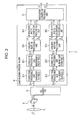
- the processing carried out by the correction processing unit 21 illustrated in Fig. 1 is carried out in parallel by a correction processing unit 21-1 and a correction processing unit 21-2
- the processing carried out by the independent correction processing unit 22 illustrated in Fig. 1 is carried out in parallel by an independent correction processing unit 22-1 and an independent correction processing unit 22-2.
- the resolution-conversion processing unit 25 illustrated in Fig. 2 carries out processing to convert the video signal Y1-1 and C1-1 supplied from the modulation and YC-conversion processing unit 24-1 and the video signal Y1-2 and C1-2 supplied from the modulation and YC-conversion processing unit 24-2 into signals conforming to the output format and outputs the obtained video signals Y2 and C2 to an external unit.
- the present invention has been conceived in light of the problems described above. Accordingly, even when the number of pixel in a solid-state image-pickup device 12 is increased, appropriate processing is compensated for within a predetermined amount of time without causing an increase in driving frequency and an increase in circuit area, and degradation in image quality is prevented.
- the first signal processing apparatus may include a second resolution conversion unit configured to carry out at least one of processing for cutting out an image in a range of effective pixels and processing for converting a progressive image signal into an interlace image signal.
- appropriate compensation can be carried out within a predetermined amount of time and degradation of image quality can be prevented even when the number of pixels in a solid-state image-pickup device is increased by neither increasing the driving frequency nor increasing the circuit area.
- An embodiment of the present invention provides a signal processing apparatus (for example a signal processing apparatus shown in Fig. 3) configured to carry out signal processing on an input image signal and to output the result of the signal processing including first correction processing means (for example, correction processing units 21-1 and 21-2) for carrying out correction processing dependent on pixels of an image-pickup device that is the output source of the image signal on the input image signal, second correction processing means (for example, independent correction processing units 22-1 and 22-2 shown in 3) for carrying out correction processing independent from pixels of the image-pickup device on a supplied image signal, synchronization processing means (for example, synchronization processing units 23-1 and 23-1) for generating RGB signals that represents a captured image and has matching spatial phases on the basis of a supplied image signal, conversion means (for example, a modulation and YC-conversion processing unit 24 shown in Fig.
- first correction processing means for example, correction processing units 21-1 and 21-2
- second correction processing means for example, independent correction processing units 22-1 and 22-2 shown in 3
- synchronization processing means
- the modulation and YC-conversion processing unit 24 carries out image-quality improvement processing, 1/ ⁇ processing, Y-signal generation processing, C-signal generation processing, and so on on the R2, G2, and B2 signals supplied from the resolution-conversion processing unit 25-1 and outputs the obtained video signals Y1 and C1 to a resolution-conversion processing unit 25-2.
- the resolution-conversion processing unit 25-1 carries out conversion processing (for example, reduction operation) on the signal S3-1 supplied from the independent correction processing unit 22-1 and the signal S3-2 supplied from the independent correction processing unit 22-2 so as to convert an image represented by these signals into an image having the same resolution as that of an image of the output format and outputs the obtained signal S4 to a synchronization processing unit 23.
- conversion processing for example, reduction operation
- the A/D converter 13 shown in Fig. 5 converts an analog signal E1 supplied from a solid-state image-pickup device 12 into a digital signal, splits the digital signal obtained after the conversion into a digital signal S1-1 and a digital signal S1-2 and outputs the digital signal S1-1 to a correction processing unit 21-1 and the digital signal S1-2 to a correction processing unit 21-2.
Landscapes
- Engineering & Computer Science (AREA)
- Multimedia (AREA)
- Signal Processing (AREA)
- Color Television Image Signal Generators (AREA)
- Studio Devices (AREA)
- Image Processing (AREA)
Applications Claiming Priority (1)
| Application Number | Priority Date | Filing Date | Title |
|---|---|---|---|
| JP2005372790A JP4320657B2 (ja) | 2005-12-26 | 2005-12-26 | 信号処理装置 |
Publications (1)
| Publication Number | Publication Date |
|---|---|
| EP1802104A2 true EP1802104A2 (de) | 2007-06-27 |
Family
ID=37989071
Family Applications (1)
| Application Number | Title | Priority Date | Filing Date |
|---|---|---|---|
| EP06026704A Withdrawn EP1802104A2 (de) | 2005-12-26 | 2006-12-22 | Signalverarbeitungsvorrichtung |
Country Status (6)
| Country | Link |
|---|---|
| US (2) | US7750946B2 (de) |
| EP (1) | EP1802104A2 (de) |
| JP (1) | JP4320657B2 (de) |
| KR (1) | KR20070068262A (de) |
| CN (1) | CN100512394C (de) |
| TW (1) | TW200810542A (de) |
Cited By (1)
| Publication number | Priority date | Publication date | Assignee | Title |
|---|---|---|---|---|
| CN109472760A (zh) * | 2019-02-01 | 2019-03-15 | 深兰人工智能芯片研究院(江苏)有限公司 | 一种校正畸变图像的方法、装置 |
Families Citing this family (8)
| Publication number | Priority date | Publication date | Assignee | Title |
|---|---|---|---|---|
| US8149285B2 (en) | 2007-09-12 | 2012-04-03 | Sanyo Electric Co., Ltd. | Video camera which executes a first process and a second process on image data |
| JP5078516B2 (ja) * | 2007-09-12 | 2012-11-21 | 三洋電機株式会社 | ビデオカメラ |
| CN101546423B (zh) * | 2008-03-24 | 2011-05-04 | 鸿富锦精密工业(深圳)有限公司 | 影像截取装置及其影像截取方法 |
| RU2453068C1 (ru) * | 2008-06-03 | 2012-06-10 | Кэнон Кабусики Кайся | Устройство захвата изображения |
| JP5359465B2 (ja) | 2009-03-31 | 2013-12-04 | ソニー株式会社 | 固体撮像装置、固体撮像装置の信号処理方法および撮像装置 |
| WO2016167016A1 (ja) * | 2015-04-14 | 2016-10-20 | ソニー株式会社 | 画像処理装置、画像処理方法、および画像処理システム |
| JP6888405B2 (ja) * | 2017-05-10 | 2021-06-16 | 富士フイルムビジネスイノベーション株式会社 | 画像処理装置及びプログラム |
| US12591780B2 (en) | 2020-02-20 | 2026-03-31 | Illumina, Inc. | Data compression for artificial intelligence-based base calling |
Family Cites Families (13)
| Publication number | Priority date | Publication date | Assignee | Title |
|---|---|---|---|---|
| JP3257145B2 (ja) | 1993-06-04 | 2002-02-18 | 松下電器産業株式会社 | 撮像装置 |
| CN1136381A (zh) * | 1994-08-31 | 1996-11-20 | 索尼公司 | 摄象装置 |
| JP3355975B2 (ja) | 1997-01-09 | 2002-12-09 | 松下電器産業株式会社 | 色信号処理回路 |
| US6356306B1 (en) * | 1997-02-28 | 2002-03-12 | Sanyo Electric Co., Ltd. | Digital camera capable of converting a progressive scan signal into an interlace scan signal |
| JPH11185031A (ja) * | 1997-12-24 | 1999-07-09 | Canon Inc | 解像度変換方法、解像度変換装置、その装置を含むシステム、及び記憶媒体 |
| JP4131052B2 (ja) * | 1998-07-17 | 2008-08-13 | ソニー株式会社 | 撮像装置 |
| US7424207B2 (en) * | 2000-02-18 | 2008-09-09 | Sanyo Electric Co., Ltd. | Digital camera |
| JP4167401B2 (ja) * | 2001-01-12 | 2008-10-15 | 富士フイルム株式会社 | ディジタル・カメラおよびその動作制御方法 |
| DE60225133T2 (de) * | 2001-05-11 | 2009-02-12 | Koninklijke Philips Electronics N.V. | Vorrichtung zur parallelen datenverarbeitung und kamerasystem mit einer solchen vorrichtung |
| US7301571B2 (en) * | 2003-01-17 | 2007-11-27 | Fujifilm Corporation | Method and imaging apparatus for correcting defective pixel of solid-state image sensor, and method for creating pixel information |
| US7295345B2 (en) * | 2003-04-29 | 2007-11-13 | Eastman Kodak Company | Method for calibration independent defect correction in an imaging system |
| JP4378994B2 (ja) * | 2003-04-30 | 2009-12-09 | ソニー株式会社 | 画像処理装置、画像処理方法ならびに撮像装置 |
| JP2005328421A (ja) * | 2004-05-17 | 2005-11-24 | Sony Corp | 撮像装置および撮像方法 |
-
2005
- 2005-12-26 JP JP2005372790A patent/JP4320657B2/ja not_active Expired - Fee Related
-
2006
- 2006-12-08 US US11/608,401 patent/US7750946B2/en not_active Expired - Fee Related
- 2006-12-12 TW TW095146365A patent/TW200810542A/zh unknown
- 2006-12-20 KR KR1020060130785A patent/KR20070068262A/ko not_active Withdrawn
- 2006-12-22 EP EP06026704A patent/EP1802104A2/de not_active Withdrawn
- 2006-12-26 CN CNB2006101705518A patent/CN100512394C/zh not_active Expired - Fee Related
-
2010
- 2010-05-18 US US12/782,343 patent/US7924319B2/en not_active Expired - Fee Related
Cited By (2)
| Publication number | Priority date | Publication date | Assignee | Title |
|---|---|---|---|---|
| CN109472760A (zh) * | 2019-02-01 | 2019-03-15 | 深兰人工智能芯片研究院(江苏)有限公司 | 一种校正畸变图像的方法、装置 |
| CN109472760B (zh) * | 2019-02-01 | 2019-05-21 | 深兰人工智能芯片研究院(江苏)有限公司 | 一种校正畸变图像的方法、装置 |
Also Published As
| Publication number | Publication date |
|---|---|
| TW200810542A (en) | 2008-02-16 |
| JP4320657B2 (ja) | 2009-08-26 |
| JP2007174560A (ja) | 2007-07-05 |
| US20070146495A1 (en) | 2007-06-28 |
| KR20070068262A (ko) | 2007-06-29 |
| US7750946B2 (en) | 2010-07-06 |
| CN1992823A (zh) | 2007-07-04 |
| US7924319B2 (en) | 2011-04-12 |
| US20100220219A1 (en) | 2010-09-02 |
| CN100512394C (zh) | 2009-07-08 |
Similar Documents
| Publication | Publication Date | Title |
|---|---|---|
| US7924319B2 (en) | Signal processing apparatus allowing an increase in pixels without an increase in driving frequency and circuit area | |
| US9055181B2 (en) | Solid-state imaging device, image processing apparatus, and a camera module having an image synthesizer configured to synthesize color information | |
| US8310568B2 (en) | Clamp control method, clamp correction device, image sensor, and electronic apparatus | |
| US11233957B2 (en) | Solid state image sensor and electronic equipment | |
| US8508625B2 (en) | Image processing apparatus | |
| US8077253B2 (en) | Solid-state device having digital signal processing circuit | |
| US20110234864A1 (en) | Imaging device | |
| US8111298B2 (en) | Imaging circuit and image pickup device | |
| JP4803156B2 (ja) | 固体撮像素子用の信号処理装置、信号処理装置を備えた撮像装置、信号処理方法、およびプログラム | |
| US8054353B2 (en) | Camera system for processing luminance and color signals using added pixel and adding sync signals | |
| US8218021B2 (en) | Image capture apparatus, method of controlling the same, and program | |
| EP2031881B1 (de) | Bilderfassungsanordnung und signalverarbeitungsverfahren | |
| KR100843195B1 (ko) | 디스플레이 처리와 데이터 압축을 동시에 수행하는 촬상신호 처리 장치 및 그 방법 | |
| JP2006148931A (ja) | 補色カラーフィルタを採用したSoCカメラシステム | |
| KR20120024448A (ko) | 촬상 장치, 신호 처리 방법 및 프로그램 | |
| US7609304B2 (en) | CCD camera with a plurality of sensor areas and corresponding output channels correcting image using a clamping process | |
| US20070285529A1 (en) | Image input device, imaging module and solid-state imaging apparatus | |
| US20070269133A1 (en) | Image-data noise reduction apparatus and method of controlling same | |
| JP2006303774A (ja) | 撮像装置 | |
| US8810710B2 (en) | Imaging using normalized luminance value to display focus state | |
| JP2000078594A (ja) | 単板式カラーカメラの広ダイナミックレンジ化処理方法 | |
| WO2019053764A1 (ja) | 撮像装置 | |
| KR100769553B1 (ko) | 색상 편차 보상 장치, 보상 방법 및 이를 이용한 이미지프로세서 | |
| KR100291442B1 (ko) | 단판식 칼라 카메라의 칼라 무아레 저감장치 | |
| JPH0888778A (ja) | 画像走査装置 |
Legal Events
| Date | Code | Title | Description |
|---|---|---|---|
| PUAI | Public reference made under article 153(3) epc to a published international application that has entered the european phase |
Free format text: ORIGINAL CODE: 0009012 |
|
| AK | Designated contracting states |
Kind code of ref document: A2 Designated state(s): AT BE BG CH CY CZ DE DK EE ES FI FR GB GR HU IE IS IT LI LT LU LV MC NL PL PT RO SE SI SK TR |
|
| AX | Request for extension of the european patent |
Extension state: AL BA HR MK YU |
|
| STAA | Information on the status of an ep patent application or granted ep patent |
Free format text: STATUS: THE APPLICATION IS DEEMED TO BE WITHDRAWN |
|
| 18D | Application deemed to be withdrawn |
Effective date: 20100701 |