EP1801863A1 - Silicon epitaxial wafer and method for manufacturing the same - Google Patents
Silicon epitaxial wafer and method for manufacturing the same Download PDFInfo
- Publication number
- EP1801863A1 EP1801863A1 EP05781511A EP05781511A EP1801863A1 EP 1801863 A1 EP1801863 A1 EP 1801863A1 EP 05781511 A EP05781511 A EP 05781511A EP 05781511 A EP05781511 A EP 05781511A EP 1801863 A1 EP1801863 A1 EP 1801863A1
- Authority
- EP
- European Patent Office
- Prior art keywords
- wafer
- single crystal
- silicon
- silicon single
- epitaxial
- Prior art date
- Legal status (The legal status is an assumption and is not a legal conclusion. Google has not performed a legal analysis and makes no representation as to the accuracy of the status listed.)
- Withdrawn
Links
Images

Classifications
-
- C—CHEMISTRY; METALLURGY
- C30—CRYSTAL GROWTH
- C30B—SINGLE-CRYSTAL GROWTH; UNIDIRECTIONAL SOLIDIFICATION OF EUTECTIC MATERIAL OR UNIDIRECTIONAL DEMIXING OF EUTECTOID MATERIAL; REFINING BY ZONE-MELTING OF MATERIAL; PRODUCTION OF A HOMOGENEOUS POLYCRYSTALLINE MATERIAL WITH DEFINED STRUCTURE; SINGLE CRYSTALS OR HOMOGENEOUS POLYCRYSTALLINE MATERIAL WITH DEFINED STRUCTURE; AFTER-TREATMENT OF SINGLE CRYSTALS OR A HOMOGENEOUS POLYCRYSTALLINE MATERIAL WITH DEFINED STRUCTURE; APPARATUS THEREFOR
- C30B29/00—Single crystals or homogeneous polycrystalline material with defined structure characterised by the material or by their shape
- C30B29/02—Elements
- C30B29/06—Silicon
-
- C—CHEMISTRY; METALLURGY
- C30—CRYSTAL GROWTH
- C30B—SINGLE-CRYSTAL GROWTH; UNIDIRECTIONAL SOLIDIFICATION OF EUTECTIC MATERIAL OR UNIDIRECTIONAL DEMIXING OF EUTECTOID MATERIAL; REFINING BY ZONE-MELTING OF MATERIAL; PRODUCTION OF A HOMOGENEOUS POLYCRYSTALLINE MATERIAL WITH DEFINED STRUCTURE; SINGLE CRYSTALS OR HOMOGENEOUS POLYCRYSTALLINE MATERIAL WITH DEFINED STRUCTURE; AFTER-TREATMENT OF SINGLE CRYSTALS OR A HOMOGENEOUS POLYCRYSTALLINE MATERIAL WITH DEFINED STRUCTURE; APPARATUS THEREFOR
- C30B15/00—Single-crystal growth by pulling from a melt, e.g. Czochralski method
-
- H—ELECTRICITY
- H10—SEMICONDUCTOR DEVICES; ELECTRIC SOLID-STATE DEVICES NOT OTHERWISE PROVIDED FOR
- H10F—INORGANIC SEMICONDUCTOR DEVICES SENSITIVE TO INFRARED RADIATION, LIGHT, ELECTROMAGNETIC RADIATION OF SHORTER WAVELENGTH OR CORPUSCULAR RADIATION
- H10F39/00—Integrated devices, or assemblies of multiple devices, comprising at least one element covered by group H10F30/00, e.g. radiation detectors comprising photodiode arrays
- H10F39/10—Integrated devices
- H10F39/12—Image sensors
-
- H—ELECTRICITY
- H10—SEMICONDUCTOR DEVICES; ELECTRIC SOLID-STATE DEVICES NOT OTHERWISE PROVIDED FOR
- H10F—INORGANIC SEMICONDUCTOR DEVICES SENSITIVE TO INFRARED RADIATION, LIGHT, ELECTROMAGNETIC RADIATION OF SHORTER WAVELENGTH OR CORPUSCULAR RADIATION
- H10F71/00—Manufacture or treatment of devices covered by this subclass
-
- H—ELECTRICITY
- H10—SEMICONDUCTOR DEVICES; ELECTRIC SOLID-STATE DEVICES NOT OTHERWISE PROVIDED FOR
- H10P—GENERIC PROCESSES OR APPARATUS FOR THE MANUFACTURE OR TREATMENT OF DEVICES COVERED BY CLASS H10
- H10P14/00—Formation of materials, e.g. in the shape of layers or pillars
- H10P14/20—Formation of materials, e.g. in the shape of layers or pillars of semiconductor materials
- H10P14/24—Formation of materials, e.g. in the shape of layers or pillars of semiconductor materials using chemical vapour deposition [CVD]
-
- H—ELECTRICITY
- H10—SEMICONDUCTOR DEVICES; ELECTRIC SOLID-STATE DEVICES NOT OTHERWISE PROVIDED FOR
- H10P—GENERIC PROCESSES OR APPARATUS FOR THE MANUFACTURE OR TREATMENT OF DEVICES COVERED BY CLASS H10
- H10P14/00—Formation of materials, e.g. in the shape of layers or pillars
- H10P14/20—Formation of materials, e.g. in the shape of layers or pillars of semiconductor materials
- H10P14/29—Formation of materials, e.g. in the shape of layers or pillars of semiconductor materials characterised by the substrates
- H10P14/2901—Materials
- H10P14/2902—Materials being Group IVA materials
- H10P14/2905—Silicon, silicon germanium or germanium
-
- H—ELECTRICITY
- H10—SEMICONDUCTOR DEVICES; ELECTRIC SOLID-STATE DEVICES NOT OTHERWISE PROVIDED FOR
- H10P—GENERIC PROCESSES OR APPARATUS FOR THE MANUFACTURE OR TREATMENT OF DEVICES COVERED BY CLASS H10
- H10P14/00—Formation of materials, e.g. in the shape of layers or pillars
- H10P14/20—Formation of materials, e.g. in the shape of layers or pillars of semiconductor materials
- H10P14/34—Deposited materials, e.g. layers
- H10P14/3402—Deposited materials, e.g. layers characterised by the chemical composition
- H10P14/3404—Deposited materials, e.g. layers characterised by the chemical composition being Group IVA materials
- H10P14/3411—Silicon, silicon germanium or germanium
-
- H—ELECTRICITY
- H10—SEMICONDUCTOR DEVICES; ELECTRIC SOLID-STATE DEVICES NOT OTHERWISE PROVIDED FOR
- H10P—GENERIC PROCESSES OR APPARATUS FOR THE MANUFACTURE OR TREATMENT OF DEVICES COVERED BY CLASS H10
- H10P36/00—Gettering within semiconductor bodies
- H10P36/20—Intrinsic gettering, i.e. thermally inducing defects by using oxygen present in the silicon body
-
- Y—GENERAL TAGGING OF NEW TECHNOLOGICAL DEVELOPMENTS; GENERAL TAGGING OF CROSS-SECTIONAL TECHNOLOGIES SPANNING OVER SEVERAL SECTIONS OF THE IPC; TECHNICAL SUBJECTS COVERED BY FORMER USPC CROSS-REFERENCE ART COLLECTIONS [XRACs] AND DIGESTS
- Y02—TECHNOLOGIES OR APPLICATIONS FOR MITIGATION OR ADAPTATION AGAINST CLIMATE CHANGE
- Y02P—CLIMATE CHANGE MITIGATION TECHNOLOGIES IN THE PRODUCTION OR PROCESSING OF GOODS
- Y02P70/00—Climate change mitigation technologies in the production process for final industrial or consumer products
- Y02P70/50—Manufacturing or production processes characterised by the final manufactured product
-
- Y—GENERAL TAGGING OF NEW TECHNOLOGICAL DEVELOPMENTS; GENERAL TAGGING OF CROSS-SECTIONAL TECHNOLOGIES SPANNING OVER SEVERAL SECTIONS OF THE IPC; TECHNICAL SUBJECTS COVERED BY FORMER USPC CROSS-REFERENCE ART COLLECTIONS [XRACs] AND DIGESTS
- Y10—TECHNICAL SUBJECTS COVERED BY FORMER USPC
- Y10T—TECHNICAL SUBJECTS COVERED BY FORMER US CLASSIFICATION
- Y10T428/00—Stock material or miscellaneous articles
- Y10T428/26—Web or sheet containing structurally defined element or component, the element or component having a specified physical dimension
- Y10T428/263—Coating layer not in excess of 5 mils thick or equivalent
- Y10T428/264—Up to 3 mils
- Y10T428/265—1 mil or less
Definitions
- the present invention relates to a silicon epitaxial wafer (hereafter referred to as an epi-wafer) which can be suitably applied to a CCD (Charge Coupled Device), CMOS (Complementally Metal-Oxide Semiconductor) or the like.
- CCD Charge Coupled Device
- CMOS Complementally Metal-Oxide Semiconductor
- a DG-IG epi-wafer having an extremely high internal gettering effect has been used for imaging devices.
- a DG-IG epi-wafer is formed by epitaxial growth of a silicon single crystal on a surface of a silicon wafer (DZ-IG wafer) which has been subjected to Denuded Zone-Intrinsic Gettering (DZ-IG) treatment.
- An imaging substrate is required to have a strong gettering effect so as to eliminate heavy metal contamination.
- an IG wafer must have oxide precipitates with high density of not less than 5 ⁇ 10 9 particles/cm 3 when the IG wafer is used for producing an imaging substrate.
- a DZ-IG wafer is produced by a two-step heat treatment comprising a DZ heat treatment at a temperature of about 1100°C to 1200°C to convert a surface layer of a wafer to a defect-free layer by outer diffusion of oxygen, and an IG heat treatment at a temperature of 600°C to 900°C to form oxygen precipitation nuclei within the wafer. Since the DG-IG heat treatment generally requires a treatment time of 10 hours or more, the production cost of the DG-IG wafer is expensive. In addition, the DZ heat treatment performed at a high temperature has allowed a possibility of contamination of the wafer with heavy metals during the heat treatment. Therefore, the DZ-IG wafer produced using the DZ-IG wafer also had a problem of high production cost and the occurrence of heavy metal contamination during the heat treatment.
- a silicon wafer is pulled by the Czochralski method (CZ method) while controlling the oxygen concentration to be in a range from 12 to 18 ⁇ 10 17 atoms/cm 3 (ASTM F121-1979), and carbon concentration to be in a range from 0.3 to 2.5 ⁇ 10 15 atoms/cm 3 (ASTM F123-1981).
- CZ method Czochralski method
- the wafer After slicing a silicon wafer from the silicon single crystal, the wafer is subjected to an annealing treatment at a temperature of not lower than 600°C and not higher than 900°C for a duration of not shorter than 15 minutes and not longer than 4 hours. Without subjecting the wafer to a treatment intended to cause an Extrinsic Gettering (EG) effect, one side or both sides of the wafer are mirror polished, and an epitaxial film is formed on the surface of the wafer.
- EG Extrinsic Gettering
- a silicon single crystal is pulled by the CZ method or by the MCZ method while controlling the carbon concentration to be in a range from 0.1 to 2.5 ⁇ 10 15 atoms/cm 3 (ASTM F123-1981), and oxygen concentration to be in a range from 10 to 18 ⁇ 10 17 atoms/cm 3 (ASTM F121-1979), and a silicon wafer for a semiconductor device is sliced from the single crystal.
- One side or both sides of the wafer is mirror polished and an epitaxial silicon film is formed on the surface of the wafer. After that, the wafer is subjected to a heat treatment for forming micro defects in the interior portion of the wafer.
- Patent Reference 3 Japanese Unexamined Patent Application, First Publication No. 2001-237247 discloses a method for producing an epi-wafer, comprising an epitaxial growth on a carbon-doped CZ wafer at a temperature below 1000°C. Using the methods described in Patent References 1 through 3, it is possible to obtain an epi-wafer which exhibits sufficient IG effect during a device process under low temperature conditions.
- Patent Reference 4 Japanese Patent Publication No. 3203740 .
- Patent Reference 4 Japanese Patent Publication No. 3203740
- epi-wafers obtained by the methods of the above-described Patent Reference 1 through 3 generated oxide precipitates to a density similar to that of the conventionally-used DG-IG epi-wafer.
- the above-described wafers had a relatively smaller density of oxide precipitates during the early stage of device formation.
- the results indicate that the above-described epi-wafers have an IG effect equivalent to the DG-IG epi-wafer during and after an intermediate stage of the device production process, but during the early stage, have an IG effect inferior to that of the De-IG epi-wafer.
- An object of the present invention is to provide a silicon epitaxial wafer and a method for producing the same which can be produced with lower production cost than that of the DG-IG wafer, has an excellent gettering effect, and is free of heavy metal contamination.
- Another object of the present invention is to provide a silicon epitaxial wafer and a method for producing the same which exhibits a strong gettering effect from the early stage of a production process of an imaging device.
- the inventors formed a polycrystalline silicon layer on the backside of a carbon-doped wafer so as to provide an EG effect. After the formation of the polycrystalline silicon layer, an epitaxial layer was formed on a surface of the wafer by epitaxial growth. Thus, a silicon epitaxial wafer of the present invention was produced.
- a first aspect of the invention is an improved configuration of a silicon epitaxial wafer comprising a silicon single crystal wafer sliced from a CZ silicon ingot doped with carbon in a range of not less than 5 ⁇ 10 15 atoms/cm 3 and not more than 5 ⁇ 10 17 atoms/cm 3 (ASTM F123-1981) and an epitaxial layer consisting of a silicon single crystal grown epitaxially on a front surface of the silicon single crystal wafer.
- a polycrystalline silicon layer having a thickness of not less than 0.5 ⁇ m and not more than 1.5 ⁇ m is formed on a back surface of the silicon single crystal wafer.
- the silicon epitaxial wafer according to the first aspect In the early stage of the production process of an imaging device, the silicon epitaxial wafer according to the first aspect generates oxide precipitates of 5 ⁇ 10 9 particles/cm 3 or more, and therefore has sufficient IG effect. In addition, an EG effect is added by the polycrystalline silicon layer. Therefore, the silicon epitaxial wafer has an optimum applicability to the production of an imaging device which is sensitive to heavy metal contamination, and contributes to improvement of the yield.
- a second aspect of the present invention is a method for producing a silicon epitaxial wafer, comprising: preparing a silicon single crystal wafer sliced from a CZ silicon ingot doped with carbon in a range of not less than 5 ⁇ 10 15 atoms/cm 3 and not more than 5 ⁇ 10 17 atoms/cm 3 (ASTM F123-1981); forming a polycrystalline silicon layer having a thickness of not less than 0.5 ⁇ m and not more than 1.5 ⁇ m on a back surface of the silicon single crystal wafer and forming oxygen precipitation nuclei in an internal portion of the silicon single crystal wafer; and epitaxially growing an epitaxial layer consisting of a silicon single crystal on a front surface of the silicon single crystal wafer.
- An epitaxial wafer of the present invention generates oxide precipitates of not less than 5 ⁇ 10 9 particles/cm 3 in the early stage of the production process of an imaging device and therefore provides a sufficient IG effect.
- an EG effect is provided by the polycrystalline silicon layer. Therefore, the silicon epitaxial wafer has an optimum applicability to the production of an imaging device which is sensitive to heavy metal contamination, and contributes to improvement of the yield.
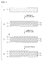
- FIG. 1C shows a silicon epitaxial wafer of the invention having an improved configuration of a silicon epitaxial wafer 10 comprising a silicon single crystal wafer 11 sliced from a CZ silicon ingot doped with carbon in a range of not less than 5 ⁇ 10 15 atoms/cm 3 and not more than 5 ⁇ 10 17 atoms/cm 3 (ASTM F123-1981), and an epitaxial layer 13 of silicon single crystal formed by epitaxial growth on a front surface of the silicon single crystal wafer 11.
- a polycrystalline silicon layer 12 is formed so as to have a thickness of not less than 0.5 ⁇ m and not more than 1.5 ⁇ m.
- oxide precipitates 11b of not less than 5 ⁇ 10 9 particles/cm 3 are generated in the early stage of the production process of an imaging device.
- the above-described silicon epitaxial wafer Since a sufficient IG effect can be obtained by the oxide precipitates, and an EG effect is provided by the polycrystalline silicon layer 12, the above-described silicon epitaxial wafer has an optimum applicability to the production of an imaging device which is sensitive to heavy metal contamination, and contributes to improvement of the yield.
- a method for producing a silicon epitaxial wafer according to the present invention is explained in the following.
- a silicon wafer 11 is prepared.
- the silicon wafer 11 has been sliced from a CZ silicon ingot doped with carbon in a range of not less than 5 ⁇ 10 15 atoms/cm 3 and not more than 5 ⁇ 10 17 atoms/cm 3 (ASTM F123-1981).
- the carbon concentration is less than 5 ⁇ 10 15 atoms/cm 3
- oxide precipitates of not less than 5 ⁇ 10 9 atoms/cm 3 in the device process resulting in insufficient gettering.
- the concentration of doped carbon was set in a range of of not less than 5 ⁇ 10 15 atoms/cm 3 and not more than 5 ⁇ 10 17 atoms/cm 3 (ASTM F123-1981).
- the concentration of doped carbon is in a range from 5 ⁇ 10 15 atoms/cm 3 and not more than 5 ⁇ 10 16 atoms/cm 3 .
- the oxygen concentration of the silicon wafer 11 is preferably in a range from 14 to 18 ⁇ 10 17 atoms/cm 3 (ASTMF121-1979). Where the oxygen concentration is less than 14 ⁇ 10 17 atoms/cm 3 , it is difficult to produce oxide precipitates of not less than 5 ⁇ 10 9 atoms/cm 3 in the device process, resulting in insufficient gettering. Where the oxygen concentration exceeds 18 ⁇ 10 17 atoms/cm 3 , epitaxial defects caused by the oxygen precipitation easily occur. Preferable oxygen concentration is in a range from 14 to 16 ⁇ 10 17 atoms/cm 3 . Specific resistivity of the silicon single crystal wafer 11 is not limited.
- a low resistivity substrate of about 0.1 ⁇ cm or less or a high resistivity substrate exceeding 100 ⁇ cm may be applied to the epitaxial wafer of the present invention.
- at least a main surface of the single crystal wafer 11 used in the invention is mirror-polished.
- a polycrystalline silicon layer 12 of average thickness of not less than 0.5 ⁇ m and not more than 1.5 ⁇ m is formed on the back surface of the silicon wafer 11, and oxygen precipitation nuclei 11a are formed in the silicon single crystal wafer 11.
- oxygen precipitation nuclei are formed within a very short period of time.
- the thickness of the polycrystalline silicon layer 12 is less than 0.5 ⁇ m, it is impossible to obtain a sufficient EG effect. Where the thickness exceeds 1.5 ⁇ m, even though a sufficient EG effect can be provided, high production cost is required and warpage in the wafer occurs. Therefore, the thickness of the polycrystalline silicon layer was set in a range of not less than 0.5 ⁇ m and not more than 1.5 ⁇ m. Preferably, the thickness of the polycrystalline silicon layer 12 is from 0.8 to 1.2 ⁇ m.
- an epitaxial layer 13 consisting of a silicon single crystal is formed by epitaxial growth on the surface of the silicon single crystal wafer 11.
- the epitaxial layer 13 has a thickness in a range from 5 to 20 ⁇ m.
- a silicon epitaxial layer 10 of the present invention can be obtained.
- This epitaxial wafer can be produced at lower production cost than that of the DZ-IG wafer.
- contamination with heavy metals does not occur in the device production process and strong gettering effect can be expected from the early stage of the production process of an imaging device.
- a silicon ingot doped with P at a concentration of 4.4 ⁇ 10 14 atoms/cm 3 and carbon at a concentration of 1 ⁇ 10 16 atoms/cm 3 (ASTM F123-1981), having an oxygen concentration of 15 ⁇ 10 17 atoms/cm 3 (ASTM F 121-1979), and having a resistvity of 10 ⁇ cm was grown by the CZ method.
- n-type silicon wafers having a diameter of 8 inches were sliced from the ingot.
- a polycrystalline silicon layer of 1 ⁇ m in thickness was formed on a backside of the silicon single crystal wafer.
- an epitaxial layer of n-type silicon single crystal having a resistivity of 10 ⁇ cm was epitaxially grown so as to have a thickness of 10 ⁇ m.
- an epitaxial wafer was obtained.
- a silicon ingot doped with P at a concentration of 4.4 ⁇ 10 14 atoms/cm 3 , having an oxygen concentration of 15 ⁇ 10 17 atoms/cm 3 (ASTM F121-1979), and having a resistvity of 10 ⁇ cm was grown by the CZ method.
- n-type silicon wafers having a diameter of 8 inches were sliced from the ingot.
- a DZ-IG wafer was formed by performing a DZ-IG two-step heat treatment comprising a first heat treatment and a second heat treatment shown in FIG 2.
- the DZ-IG heat treatment was performed under a N 2 gas atmosphere containing 3% O 2 .
- An epitaxial wafer was obtained by epitaxial growth of an n-type silicon single crystal having a resistivity of 10 ⁇ cm and a thickness of 10 ⁇ m on the surface of an n-type silicon single crystal wafer sliced from an ingot of Example 1. Different from Example 1, a polycrystalline silicon layer was not formed on the back surface of the wafer.
- An epitaxial wafer was obtained by epitaxial growth of arn n-type silicon single crystal having a resistivity of 10 ⁇ cm and a thickness of 10 ⁇ m on the surface of an n-type silicon single crystal wafer sliced from an ingot of Comparative Example 1. Different from DZ-IG epi-wafer obtained in Comparative Example 1, a DZ-IG two-step heat treatment was not performed on the wafer.
- each sample was subjected to a heat treatment for simulating a CCD production process.
- the early stage of device production, intermediate stage, and final stage were respectively simulated.
- sample wafer was extracted.
- Each sample was divided into a tablet along a cleavage, and the cleaved wafer was subjected to selective chemical etching (wright etching) of 2 ⁇ m so as to visualize oxide precipitates.
- the density of oxide precipitates on the sectional plane of the wafer was measured using an optical microscope. The result is shown in FIG. 3.
- FIG 3 denotes a result of measurement of the oxide precipitates density of each wafer after the epitaxial growth and before the heat treatment.
- the down arrows in FIG 3 respectively show that the oxide precipitate density of as Epi, and oxygen precipitation density of Comparative example are respectively below the detection limit.
- oxide precipitates were not observed in the early stage of the device process, whereas oxide precipitates providing a sufficient gettering effect were observed in the intermediate stage of the device process.
- oxide precipitate density did not reach a level sufficient for gettering even at a final stage of the device process.
- oxide precipitate densities of not less than 5 ⁇ 10 9 particles /cm 3 sufficient for providing gettering ability were observed from the early stage of device production.
- Example 1 and Comparative Examples 1 through 3 Surfaces of the epi-wafers obtained by Example 1 and Comparative Examples 1 through 3 were respectively contaminated by compulsion with Ni in a concentration of 1 ⁇ 10 12 atoms/cm 2 .
- the compulsively Ni-contaminated epi-wafers were respectively subjected to the heat treatment simulation of the Comparative Testing 1 simulating the CCD production process to the final stage.
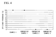
- each epi-wafer was subjected to evaluation of dielectric strength of the oxide film based on TZDB (Time Zero Dielectric Breakdown) under the conditions of a gate oxide film of 10 nm, and evaluation voltage of 8MV/cm. Efficiency percentage in this testing is shown in FIG. 4.
- TZDB Time Zero Dielectric Breakdown
- p/p- and p/p+ wafers comprising a carbon-doped p-type wafer and a polycrystalline silicon layer formed on the wafer were prepared. These wafers were subjected to a simulation-heat treatment equivalent to a CMOS image sensor process production process to a final stage. After the heat treatment simulation each wafer was subjected to evaluation of the dielectric strength of the oxide film based on TZDB. As a result all the tips showed satisfactory results, that is, the efficiency percentage was 100%.
- the epi-wafer according to the present invention comprising a carbon-doped wafer, a polycrystalline silicon layer formed on the back surface of the wafer, and an epitaxial layer formed on the front surface of the wafer provides high-yields even in a epi-wafer having a base of a p-type wafer.
- An epitaxial wafer according to the present invention provides a sufficient IG effect by the formation of oxide precipitates during an early stage of the production process of an imaging device, and further provides an EG effect by the polycrystalline silicon layer. Therefore, the epitaxial wafer has an optimum applicability to the production of an imaging device which is sensitive to heavy metal contamination, and contributes to improvement of the yield.
- a method for producing an epitaxial wafer according to the present invention enables the production of epitaxial wafers at lower cost than that of the DZ-IG wafer which requires a high production cost and has a high possibility of heavy metal contamination occurring during its production process.
- contamination with heavy metals does not occur during the production process of the wafers and a strong gettering effect is expected from the early stage of the production process of the imaging device.
Landscapes
- Chemical & Material Sciences (AREA)
- Engineering & Computer Science (AREA)
- Crystallography & Structural Chemistry (AREA)
- Materials Engineering (AREA)
- Metallurgy (AREA)
- Organic Chemistry (AREA)
- Recrystallisation Techniques (AREA)
- Crystals, And After-Treatments Of Crystals (AREA)
- Solid State Image Pick-Up Elements (AREA)
Abstract
A silicon epitaxial wafer of the invention comprises a silicon single crystal wafer sliced from a CZ silicon ingot doped with carbon in a concentration range of not less than 5×10¹⁵atoms/cm3 and not more than 5×10¹⁷atoms/cm3 and an epitaxial layer consisting of a silicon single crystal epitaxially grown on a front surface of the silicon single crystal wafer. A polycrystalline silicon layer having a thickness of not less than 0.5 µm and not more than 1.5 µm is formed on a back surface of the silicon single crystal wafer.
Description
- The present invention relates to a silicon epitaxial wafer (hereafter referred to as an epi-wafer) which can be suitably applied to a CCD (Charge Coupled Device), CMOS (Complementally Metal-Oxide Semiconductor) or the like. Priority is claimed on
Japanese Patent Application No. 2004-251837, filed August 31, 2004 - In accordance with the recent circulation of digital cameras or the like, there has been a rapid increase in the production of imaging elements such as CCD devices and CMOS imaging censors. Where a white defect occurs in an imaging element, an image cannot be captured at the position of the white defect. Therefore, a white defect causes a problem of reducing the yield of the imaging device.
- It is known that the white defect is caused by contamination of heavy metals in a silicon wafer. Conventionally, a DG-IG epi-wafer having an extremely high internal gettering effect has been used for imaging devices. A DG-IG epi-wafer is formed by epitaxial growth of a silicon single crystal on a surface of a silicon wafer (DZ-IG wafer) which has been subjected to Denuded Zone-Intrinsic Gettering (DZ-IG) treatment. An imaging substrate is required to have a strong gettering effect so as to eliminate heavy metal contamination. It is known that an IG wafer must have oxide precipitates with high density of not less than 5×10⁹ particles/cm3 when the IG wafer is used for producing an imaging substrate. A DZ-IG wafer is produced by a two-step heat treatment comprising a DZ heat treatment at a temperature of about 1100°C to 1200°C to convert a surface layer of a wafer to a defect-free layer by outer diffusion of oxygen, and an IG heat treatment at a temperature of 600°C to 900°C to form oxygen precipitation nuclei within the wafer. Since the DG-IG heat treatment generally requires a treatment time of 10 hours or more, the production cost of the DG-IG wafer is expensive. In addition, the DZ heat treatment performed at a high temperature has allowed a possibility of contamination of the wafer with heavy metals during the heat treatment. Therefore, the DZ-IG wafer produced using the DZ-IG wafer also had a problem of high production cost and the occurrence of heavy metal contamination during the heat treatment.
- Expedients to solve the above-described problem have been proposed. For example, in a method for producing a silicon wafer disclosed in Patent Reference 1 (
Japanese Unexamined Patent Application, First Publication No. H10-229093 - In a method for producing an epitaxial wafer disclosed in Patent Reference 2 (
Japanese Unexamined Patent Application, First Publication H11-204534 - For example, Patent Reference 3 (
Japanese Unexamined Patent Application, First Publication No. 2001-237247 Patent References 1 through 3, it is possible to obtain an epi-wafer which exhibits sufficient IG effect during a device process under low temperature conditions. - There is a method disclosed for producing a semiconductor device, comprising a step of forming an EG layer on the back surface of a semiconductor wafer and a step of implanting elements constituting oxygen precipitation nuclei into an interstitial portion between the EG layer and element-forming region of the semiconductor wafer (for example, Patent Reference 4:
Japanese Patent Publication No. 3203740 - In a method for producing an epitaxial wafer disclosed in Patent Reference 5 (
Japanese Patent Publication No. 3173106 - In an equivalent heat treatment for simulating a production process for CCD, epi-wafers obtained by the methods of the above-described
Patent Reference 1 through 3 generated oxide precipitates to a density similar to that of the conventionally-used DG-IG epi-wafer. However, compared with the conventional DZ-IG epi-wafer, the above-described wafers had a relatively smaller density of oxide precipitates during the early stage of device formation. The results indicate that the above-described epi-wafers have an IG effect equivalent to the DG-IG epi-wafer during and after an intermediate stage of the device production process, but during the early stage, have an IG effect inferior to that of the De-IG epi-wafer. - In the method described in Patent Reference 4, high cost and long duration required for the ion implantation are economically undesirable, and a sufficient gettering effect cannot be obtained since the oxygen precipitation region is limited to a region having a very narrow distribution in the depth direction. The method described in Patent Reference 5 cannot achieve a sufficient gettering effect since the oxygen precipitation region is limited to the gettering layer formed on the back surface of the substrate.
- An object of the present invention is to provide a silicon epitaxial wafer and a method for producing the same which can be produced with lower production cost than that of the DG-IG wafer, has an excellent gettering effect, and is free of heavy metal contamination.
- Another object of the present invention is to provide a silicon epitaxial wafer and a method for producing the same which exhibits a strong gettering effect from the early stage of a production process of an imaging device.
- In order to solve the above-described problem, the inventors formed a polycrystalline silicon layer on the backside of a carbon-doped wafer so as to provide an EG effect. After the formation of the polycrystalline silicon layer, an epitaxial layer was formed on a surface of the wafer by epitaxial growth. Thus, a silicon epitaxial wafer of the present invention was produced.
- A first aspect of the invention is an improved configuration of a silicon epitaxial wafer comprising a silicon single crystal wafer sliced from a CZ silicon ingot doped with carbon in a range of not less than 5×10¹⁵atoms/cm3 and not more than 5×10¹⁷atoms/cm3 (ASTM F123-1981) and an epitaxial layer consisting of a silicon single crystal grown epitaxially on a front surface of the silicon single crystal wafer. In this aspect, a polycrystalline silicon layer having a thickness of not less than 0.5 µm and not more than 1.5 µm is formed on a back surface of the silicon single crystal wafer.
- In the early stage of the production process of an imaging device, the silicon epitaxial wafer according to the first aspect generates oxide precipitates of 5×10⁹ particles/cm3 or more, and therefore has sufficient IG effect. In addition, an EG effect is added by the polycrystalline silicon layer. Therefore, the silicon epitaxial wafer has an optimum applicability to the production of an imaging device which is sensitive to heavy metal contamination, and contributes to improvement of the yield.
- A second aspect of the present invention is a method for producing a silicon epitaxial wafer, comprising: preparing a silicon single crystal wafer sliced from a CZ silicon ingot doped with carbon in a range of not less than 5×10¹⁵atoms/cm3 and not more than 5×10¹⁷atoms/cm3 (ASTM F123-1981); forming a polycrystalline silicon layer having a thickness of not less than 0.5 µm and not more than 1.5 µm on a back surface of the silicon single crystal wafer and forming oxygen precipitation nuclei in an internal portion of the silicon single crystal wafer; and epitaxially growing an epitaxial layer consisting of a silicon single crystal on a front surface of the silicon single crystal wafer.
- In the production method according to the second aspect, by performing the above-described steps in the above-described order, it is possible to produce epitaxial wafers at lower cost than that of the DZ-IG wafer. In addition, since there is no need for a high-temperature heat treatment, contamination with heavy metals does not occur during the production process of the wafer. In such an epitaxial wafer, it is possible to expect a strong gettering effect acting from the early stage of the production process of an imaging device.
- An epitaxial wafer of the present invention generates oxide precipitates of not less than 5×10⁹particles/cm3 in the early stage of the production process of an imaging device and therefore provides a sufficient IG effect. In addition, an EG effect is provided by the polycrystalline silicon layer. Therefore, the silicon epitaxial wafer has an optimum applicability to the production of an imaging device which is sensitive to heavy metal contamination, and contributes to improvement of the yield.
- By a method for producing an epitaxial wafer according to the invention, it is possible to produce an epitaxial wafer at lower cost than that of the DZ-IG wafer, which requires high production cost and has a high possibility of heavy metal contamination occurring in its production process. In addition, since there is no need for a high-temperature heat treatment, contamination with heavy metals does not occur in the device production process and a strong gettering effect can be expected from the early stage of the production process of an imaging device.
-
- FIGS. 1A through D are drawings showing a process chart of a method for producing a silicon epitaxial wafer of the present invention.
- FIG. 2 is a graph showing a thermal profile of a DZ-IG two-step heat treatment of Comparative Example 1.
- FIG 3 shows densities of oxide precipitates for each of device processing steps in the
Comparative Testing 1. - FIG 4 is a graph showing efficiency percentage under evaluation testing of dielectric voltage of an oxide layer by TZDB in the
Comparative Testing 2. -
- 10
- silicon epitaxial wafer
- 11
- silicon single crystal wafer
- 11a
- oxygen precipitation nuclei
- 11b
- oxide precipitate
- 12
- polycrystalline silicon layer
- 13
- epitaxial silicon layer
- Next, a best mode for carrying out the invention is explained with reference to the drawings.
- FIG. 1C shows a silicon epitaxial wafer of the invention having an improved configuration of a
silicon epitaxial wafer 10 comprising a siliconsingle crystal wafer 11 sliced from a CZ silicon ingot doped with carbon in a range of not less than 5×10¹⁵atoms/cm3 and not more than 5×10¹⁷atoms/cm3 (ASTM F123-1981), and anepitaxial layer 13 of silicon single crystal formed by epitaxial growth on a front surface of the siliconsingle crystal wafer 11. On a back surface of the siliconsingle crystal wafer 11, apolycrystalline silicon layer 12 is formed so as to have a thickness of not less than 0.5µm and not more than 1.5µm. - By forming the
polycrystalline silicon layer 12 on the back surface of the siliconsingle crystal wafer 11, in addition to the EG effect of thepolycrystalline silicon layer 12, it is possible to obtain an effect of enhancing oxygen precipitation within the wafer by introducing vacancies from thepolycrystalline silicon layer 12 into the interior of the siliconsingle crystal wafer 11. Therefore, numerous oxide precipitates are formed within the siliconsingle crystal wafer 11. By using such an epitaxial wafer, as shown in FIG 1D, oxide precipitates 11b of not less than 5×10⁹particles/cm3 are generated in the early stage of the production process of an imaging device. Since a sufficient IG effect can be obtained by the oxide precipitates, and an EG effect is provided by thepolycrystalline silicon layer 12, the above-described silicon epitaxial wafer has an optimum applicability to the production of an imaging device which is sensitive to heavy metal contamination, and contributes to improvement of the yield. - Next, a method for producing a silicon epitaxial wafer according to the present invention is explained in the following. Firstly, as shown in FIG.1A, a
silicon wafer 11 is prepared. Thesilicon wafer 11 has been sliced from a CZ silicon ingot doped with carbon in a range of not less than 5×10¹⁵atoms/cm3 and not more than 5×10¹⁷atoms/cm3 (ASTM F123-1981). Where the carbon concentration is less than 5×10¹⁵atoms/cm3, it is difficult to generate oxide precipitates of not less than 5×10⁹atoms/cm3 in the device process, resulting in insufficient gettering. Where the carbon concentration exceeds 5×10¹⁷atoms/cm3, it is impossible to grow a single crystal because of generation of dislocations in the crystal. Therefore, the concentration of doped carbon was set in a range of of not less than 5×10¹⁵atoms/cm3 and not more than 5×10¹⁷atoms/cm3 (ASTM F123-1981). Preferably, the concentration of doped carbon is in a range from 5×10¹⁵atoms/cm3 and not more than 5×10¹⁶atoms/cm3. - The oxygen concentration of the
silicon wafer 11 is preferably in a range from 14 to 18×1017atoms/cm3(ASTMF121-1979). Where the oxygen concentration is less than 14×1017atoms/cm3, it is difficult to produce oxide precipitates of not less than 5×10⁹ atoms/cm3 in the device process, resulting in insufficient gettering. Where the oxygen concentration exceeds 18×1017atoms/cm3, epitaxial defects caused by the oxygen precipitation easily occur. Preferable oxygen concentration is in a range from 14 to 16×1017atoms/cm3. Specific resistivity of the siliconsingle crystal wafer 11 is not limited. Even a low resistivity substrate of about 0.1Ω·cm or less or a high resistivity substrate exceeding 100Ω·cm may be applied to the epitaxial wafer of the present invention. Preferably, at least a main surface of thesingle crystal wafer 11 used in the invention is mirror-polished. - Next, as shown in FIG.1B, a
polycrystalline silicon layer 12 of average thickness of not less than 0.5µm and not more than 1.5µm is formed on the back surface of thesilicon wafer 11, andoxygen precipitation nuclei 11a are formed in the siliconsingle crystal wafer 11. In general, it takes several hours at a temperature of about 650°C to form a polycrystalline silicon layer on the back surface of a silicon single crystal wafer. However, when a carbon-doped siliconsingle crystal wafer 11 is subjected to a heat treatment at a temperature of about 650°C, oxygen precipitation nuclei are formed within a very short period of time. In addition, by the formation of thepolycrystalline silicon layer 12 on the back surface of the siliconsingle crystal wafer 11, vacancies are provided from thepolycrystalline silicon layer 12 into the siliconsingle crystal wafer 11 and it is also possible to obtain the effect of enhancing oxygen precipitation in the wafer. Therefore, by the formation of thepolycrystalline layer 12 on the back surface of the siliconsingle crystal wafer 11, numerous oxide precipitates are formed in the siliconsingle crystal wafer 11. The introduction of vacancies into the wafer interior from a polycrystalline silicon layer is also reported in Appl. Phys. Lett., Vo1.54, No.18, 1 May1989, p.1748-1750. - Where the thickness of the
polycrystalline silicon layer 12 is less than 0.5 µm, it is impossible to obtain a sufficient EG effect. Where the thickness exceeds 1.5 µm, even though a sufficient EG effect can be provided, high production cost is required and warpage in the wafer occurs. Therefore, the thickness of the polycrystalline silicon layer was set in a range of not less than 0.5 µm and not more than 1.5 µm. Preferably, the thickness of thepolycrystalline silicon layer 12 is from 0.8 to 1.2 µm. - Next, as shown in FIG. 1C, an
epitaxial layer 13 consisting of a silicon single crystal is formed by epitaxial growth on the surface of the siliconsingle crystal wafer 11. Preferably, theepitaxial layer 13 has a thickness in a range from 5 to 20 µm. - By performing the above-described steps in the above-described order, a
silicon epitaxial layer 10 of the present invention can be obtained. This epitaxial wafer can be produced at lower production cost than that of the DZ-IG wafer. In addition, since there is no need for a high temperature heat treatment, contamination with heavy metals does not occur in the device production process and strong gettering effect can be expected from the early stage of the production process of an imaging device. - Next, an example of the invention and comparative examples are explained in detail.
- Firstly, a silicon ingot doped with P at a concentration of 4.4×10¹⁴atoms/cm3 and carbon at a concentration of 1×10¹⁶atoms/cm3(ASTM F123-1981), having an oxygen concentration of 15×1017atoms/cm3(ASTM F 121-1979), and having a resistvity of 10Ω·cm was grown by the CZ method. Then, n-type silicon wafers having a diameter of 8 inches were sliced from the ingot. Next, a polycrystalline silicon layer of 1 µm in thickness was formed on a backside of the silicon single crystal wafer. Next, on the front surface of the silicon single crystal wafer, an epitaxial layer of n-type silicon single crystal having a resistivity of 10 Ω·cm was epitaxially grown so as to have a thickness of 10µm. Thus, an epitaxial wafer was obtained.
- Firstly, a silicon ingot doped with P at a concentration of 4.4×10¹⁴ atoms/cm3, having an oxygen concentration of 15×1017atoms/cm3(ASTM F121-1979), and having a resistvity of 10Ω·cm was grown by the CZ method. Then n-type silicon wafers having a diameter of 8 inches were sliced from the ingot. Next, a DZ-IG wafer was formed by performing a DZ-IG two-step heat treatment comprising a first heat treatment and a second heat treatment shown in FIG 2. The DZ-IG heat treatment was performed under a N2 gas atmosphere containing 3% O2. Next on the surface of the DZ-IG wafer, an epitaxial layer of n-type silicon single crystal having a resistivity of 10Ω·cm was epitaxially grown so as to have a thickness of 10 µm. Thus a DZ-IG epi-wafer was obtained.
- An epitaxial wafer was obtained by epitaxial growth of an n-type silicon single crystal having a resistivity of 10Ω·cm and a thickness of 10 µm on the surface of an n-type silicon single crystal wafer sliced from an ingot of Example 1. Different from Example 1, a polycrystalline silicon layer was not formed on the back surface of the wafer.
- An epitaxial wafer was obtained by epitaxial growth of arn n-type silicon single crystal having a resistivity of 10 Ω·cm and a thickness of 10 µm on the surface of an n-type silicon single crystal wafer sliced from an ingot of Comparative Example 1. Different from DZ-IG epi-wafer obtained in Comparative Example 1, a DZ-IG two-step heat treatment was not performed on the wafer.
- Using epi-wafers obtained by Example 1 and Comparative Examples 1 through 3 as samples, each sample was subjected to a heat treatment for simulating a CCD production process. In this heat treatment simulation, the early stage of device production, intermediate stage, and final stage were respectively simulated. After each step of early stage of device process, intermediate stage, and final stage, sample wafer was extracted. Each sample was divided into a tablet along a cleavage, and the cleaved wafer was subjected to selective chemical etching (wright etching) of 2 µm so as to visualize oxide precipitates. Using these samples, the density of oxide precipitates on the sectional plane of the wafer was measured using an optical microscope. The result is shown in FIG. 3. The term "as Epi" in FIG. 3 denotes a result of measurement of the oxide precipitates density of each wafer after the epitaxial growth and before the heat treatment. The down arrows in FIG 3 respectively show that the oxide precipitate density of as Epi, and oxygen precipitation density of Comparative example are respectively below the detection limit.
- As is obvious from FIG 3, in the epi-wafer of Comparative Example 2, oxide precipitates were not observed in the early stage of the device process, whereas oxide precipitates providing a sufficient gettering effect were observed in the intermediate stage of the device process. In the epi-
wafer 3 of Comparative Example 3, the oxide precipitate density did not reach a level sufficient for gettering even at a final stage of the device process. On the other hand, in the DZ-IG epi-wafer of Comparative Example 1, and epi-wafer of Example 1, oxide precipitate densities of not less than 5×10⁹particles /cm3 sufficient for providing gettering ability were observed from the early stage of device production. - Surfaces of the epi-wafers obtained by Example 1 and Comparative Examples 1 through 3 were respectively contaminated by compulsion with Ni in a concentration of 1×10¹²atoms/cm2. Next, the compulsively Ni-contaminated epi-wafers were respectively subjected to the heat treatment simulation of the
Comparative Testing 1 simulating the CCD production process to the final stage. After the heat treatment simulation, each epi-wafer was subjected to evaluation of dielectric strength of the oxide film based on TZDB (Time Zero Dielectric Breakdown) under the conditions of a gate oxide film of 10 nm, and evaluation voltage of 8MV/cm. Efficiency percentage in this testing is shown in FIG. 4. - As is obvious from FIG 4, in the epi-wafer of Comparative Examples 2 and 3, all tips experienced dielectric breakdown and the efficiency percentages were 0%. On the other hand, in Example 1 and Comparative Example 1, all the tips showed satisfactory results, that is, the efficiency percentage was 100%. It can be interpreted that the epi-wafers of Example 1 and Comparative Example 1 had a sufficient gettering effect at an early stage of the device process, and defects were not formed on the surface of the epi-wafers. On the other hand, it is interpreted that Ni silicide was present in epi-wafers of Comparative Example 2 and Comparative Example 3 because of insufficient gettering, and showed a deteriorated dielectric strength of the oxide film.
- Next, p/p- and p/p+ wafers comprising a carbon-doped p-type wafer and a polycrystalline silicon layer formed on the wafer were prepared. These wafers were subjected to a simulation-heat treatment equivalent to a CMOS image sensor process production process to a final stage. After the heat treatment simulation each wafer was subjected to evaluation of the dielectric strength of the oxide film based on TZDB. As a result all the tips showed satisfactory results, that is, the efficiency percentage was 100%. Thus, it was confirmed that the epi-wafer according to the present invention comprising a carbon-doped wafer, a polycrystalline silicon layer formed on the back surface of the wafer, and an epitaxial layer formed on the front surface of the wafer provides high-yields even in a epi-wafer having a base of a p-type wafer.
- An epitaxial wafer according to the present invention provides a sufficient IG effect by the formation of oxide precipitates during an early stage of the production process of an imaging device, and further provides an EG effect by the polycrystalline silicon layer. Therefore, the epitaxial wafer has an optimum applicability to the production of an imaging device which is sensitive to heavy metal contamination, and contributes to improvement of the yield.
- A method for producing an epitaxial wafer according to the present invention enables the production of epitaxial wafers at lower cost than that of the DZ-IG wafer which requires a high production cost and has a high possibility of heavy metal contamination occurring during its production process. In addition, since there is no need for a high temperature heat treatment, contamination with heavy metals does not occur during the production process of the wafers and a strong gettering effect is expected from the early stage of the production process of the imaging device.
Claims (2)
- A silicon epitaxial wafer comprising:a silicon single crystal wafer sliced from a CZ silicon ingot doped with carbon in a concentration range of not less than 5×10¹⁵atoms/cm3 and not more than 5×10¹⁷ atoms/cm3 based on analysis in accordance with ASTM F123-1981;an epitaxial layer consisting of a silicon single crystal epitaxially grown on a front surface of the silicon single crystal wafer; anda polycrystalline silicon layer having a thickness of not less than 0.5 µm and not more than 1.5 µm and is formed on a back surface of the silicon single crystal wafer.
- A method for producing a silicon epitaxial wafer comprising:preparing a silicon single crystal wafer sliced from a CZ silicon ingot doped with carbon in a concentration range of not less than 5×10¹⁵atoms/cm3 and not more than 5×10¹⁷atoms/cm3 based on analysis in accordance with ASTM F123-1981;forming a polycrystalline silicon layer having a thickness of not less than 0.5 µm and not more than 1.5 µm on a back surface of the silicon single crystal wafer and forming oxygen precipitation nuclei in an interior portion of the silicon single crystal wafer; andepitaxially growing an epitaxial layer consisting of a silicon single crystal on a front surface of the silicon single crystal wafer.
Applications Claiming Priority (2)
| Application Number | Priority Date | Filing Date | Title |
|---|---|---|---|
| JP2004251837A JP2006073580A (en) | 2004-08-31 | 2004-08-31 | Silicon epitaxial wafer and manufacturing method thereof |
| PCT/JP2005/015801 WO2006025409A1 (en) | 2004-08-31 | 2005-08-30 | Silicon epitaxial wafer and method for manufacturing the same |
Publications (2)
| Publication Number | Publication Date |
|---|---|
| EP1801863A1 true EP1801863A1 (en) | 2007-06-27 |
| EP1801863A4 EP1801863A4 (en) | 2008-09-24 |
Family
ID=36000059
Family Applications (1)
| Application Number | Title | Priority Date | Filing Date |
|---|---|---|---|
| EP05781511A Withdrawn EP1801863A4 (en) | 2004-08-31 | 2005-08-30 | SILICON EPITAXIAL WAFER AND METHOD FOR MANUFACTURING SAME |
Country Status (6)
| Country | Link |
|---|---|
| US (2) | US20090017291A1 (en) |
| EP (1) | EP1801863A4 (en) |
| JP (1) | JP2006073580A (en) |
| KR (1) | KR100877772B1 (en) |
| TW (1) | TWI278040B (en) |
| WO (1) | WO2006025409A1 (en) |
Cited By (4)
| Publication number | Priority date | Publication date | Assignee | Title |
|---|---|---|---|---|
| EP2112254A2 (en) * | 2008-03-05 | 2009-10-28 | Sumco Corporation | Silicon substrate and manufacturing method thereof |
| EP2061082A4 (en) * | 2006-09-07 | 2013-04-24 | Sumco Corp | SEMICONDUCTOR SUBSTRATE FOR SEMICONDUCTOR IMAGE FORMING DEVICE, SEMICONDUCTOR IMAGE FORMING DEVICE, AND METHOD FOR MANUFACTURING SAME |
| EP2722423A3 (en) * | 2009-03-25 | 2014-07-09 | Sumco Corporation | Silicon wafer and manufacturing method thereof |
| DE112010002747B4 (en) * | 2009-06-29 | 2020-12-24 | Sumco Corporation | Method of manufacturing a silicon epitaxial wafer |
Families Citing this family (20)
| Publication number | Priority date | Publication date | Assignee | Title |
|---|---|---|---|---|
| JP2007273959A (en) * | 2006-03-06 | 2007-10-18 | Matsushita Electric Ind Co Ltd | Photodetector and manufacturing method thereof |
| TW200936825A (en) * | 2007-12-11 | 2009-09-01 | Sumco Corp | Silicon substrate and manufacturing method thereof |
| JP5568837B2 (en) * | 2008-02-29 | 2014-08-13 | 株式会社Sumco | Silicon substrate manufacturing method |
| JP5401808B2 (en) * | 2008-03-05 | 2014-01-29 | 株式会社Sumco | Silicon substrate and manufacturing method thereof |
| JP5401809B2 (en) * | 2008-03-05 | 2014-01-29 | 株式会社Sumco | Silicon substrate and manufacturing method thereof |
| JP5343371B2 (en) * | 2008-03-05 | 2013-11-13 | 株式会社Sumco | Silicon substrate and manufacturing method thereof |
| JP2010040609A (en) * | 2008-07-31 | 2010-02-18 | Sumco Corp | Epitaxial silicon wafer and manufacturing method thereof |
| JP2010050249A (en) * | 2008-08-21 | 2010-03-04 | Sumco Corp | Method of manufacturing wafer for backside illuminated solid-state imaging device |
| JP2010114211A (en) * | 2008-11-05 | 2010-05-20 | Shin Etsu Handotai Co Ltd | Method of manufacturing epitaxial silicon wafer |
| JP2010232420A (en) * | 2009-03-27 | 2010-10-14 | Sumco Corp | Wafer for back-illuminated solid-state image sensor, manufacturing method thereof, and back-illuminated solid-state image sensor |
| US20120049330A1 (en) * | 2009-05-15 | 2012-03-01 | Sumco Corporation | Silicon wafer and method for producing the same |
| JP2011054821A (en) * | 2009-09-03 | 2011-03-17 | Sumco Corp | Method of producing epitaxial wafer and epitaxial wafer |
| JP5544859B2 (en) | 2009-12-15 | 2014-07-09 | 信越半導体株式会社 | Manufacturing method of silicon epitaxial wafer |
| US9634098B2 (en) | 2013-06-11 | 2017-04-25 | SunEdison Semiconductor Ltd. (UEN201334164H) | Oxygen precipitation in heavily doped silicon wafers sliced from ingots grown by the Czochralski method |
| CN103779372A (en) * | 2014-02-10 | 2014-05-07 | 中国电子科技集团公司第四十四研究所 | CCD manufacturing technology based on non-intrinsic impurity adsorbing technology |
| JP2015008314A (en) * | 2014-08-14 | 2015-01-15 | 株式会社Sumco | Method of producing epitaxial wafer and epitaxial wafer |
| JP6447351B2 (en) | 2015-05-08 | 2019-01-09 | 株式会社Sumco | Method for manufacturing silicon epitaxial wafer and silicon epitaxial wafer |
| DE102015121890A1 (en) * | 2015-12-15 | 2017-06-22 | Infineon Technologies Ag | Process for processing a semiconductor wafer |
| US10170312B2 (en) * | 2017-04-20 | 2019-01-01 | Taiwan Semiconductor Manufacturing Company Ltd. | Semiconductor substrate and manufacturing method of the same |
| CN114050190B (en) * | 2021-11-19 | 2024-02-13 | 常州时创能源股份有限公司 | Double-sided passivation contact battery and preparation method thereof |
Family Cites Families (22)
| Publication number | Priority date | Publication date | Assignee | Title |
|---|---|---|---|---|
| EP0120830B1 (en) * | 1983-02-14 | 1992-07-15 | MEMC Electronic Materials, Inc. | Semiconductor substrate materials having enhanced gettering ability |
| US4608096A (en) * | 1983-04-04 | 1986-08-26 | Monsanto Company | Gettering |
| JP2726583B2 (en) * | 1991-11-18 | 1998-03-11 | 三菱マテリアルシリコン株式会社 | Semiconductor substrate |
| JP2874618B2 (en) * | 1995-11-22 | 1999-03-24 | 日本電気株式会社 | Silicon semiconductor substrate and method of manufacturing the same |
| DE69736900T2 (en) * | 1996-07-29 | 2007-09-06 | Sumco Corp. | METHOD FOR PRODUCING AN EPITAXIAL DISC FROM SILICON |
| JP4013276B2 (en) * | 1997-02-17 | 2007-11-28 | 株式会社Sumco | Manufacturing method of silicon epitaxial wafer |
| KR100253392B1 (en) * | 1997-12-29 | 2000-05-01 | 김영환 | Wiring fabrication method for semiconductor device |
| JPH11204534A (en) * | 1998-01-14 | 1999-07-30 | Sumitomo Metal Ind Ltd | Method for manufacturing silicon epitaxial wafer |
| JP4107628B2 (en) * | 1999-11-26 | 2008-06-25 | 株式会社Sumco | Pre-heat treatment method for imparting IG effect to silicon wafer |
| US6491752B1 (en) * | 1999-07-16 | 2002-12-10 | Sumco Oregon Corporation | Enhanced n-type silicon material for epitaxial wafer substrate and method of making same |
| JP2001102386A (en) * | 1999-10-01 | 2001-04-13 | Toshiba Ceramics Co Ltd | Method for manufacturing semiconductor wafer |
| JP2001237247A (en) * | 2000-02-25 | 2001-08-31 | Shin Etsu Handotai Co Ltd | Method of manufacturing epitaxial wafer, epitaxial wafer and cz silicon wafer for epitaxial growth |
| KR100792773B1 (en) * | 2000-04-14 | 2008-01-11 | 신에쯔 한도타이 가부시키가이샤 | Silicon Wafer, Silicon Epitaxial Wafer, Anneal Wafer and Manufacturing Method |
| US7160385B2 (en) * | 2003-02-20 | 2007-01-09 | Sumitomo Mitsubishi Silicon Corporation | Silicon wafer and method for manufacturing the same |
| KR100917087B1 (en) * | 2000-09-19 | 2009-09-15 | 엠이엠씨 일렉트로닉 머티리얼즈 인코포레이티드 | Nitrogen-doped silicon substantially free of oxidation induced stacking faults |
| JP2002164512A (en) * | 2000-11-28 | 2002-06-07 | Fujitsu Ltd | Semiconductor device and manufacturing method thereof |
| KR20030035152A (en) * | 2001-10-30 | 2003-05-09 | 주식회사 하이닉스반도체 | Method for fabricating semiconductor wafer |
| JP4656788B2 (en) * | 2001-11-19 | 2011-03-23 | 信越半導体株式会社 | Manufacturing method of silicon epitaxial wafer |
| JP2003188176A (en) * | 2001-12-18 | 2003-07-04 | Komatsu Electronic Metals Co Ltd | Silicon wafer and method for manufacturing silicon wafer |
| EP1542269B1 (en) * | 2002-07-17 | 2016-10-05 | Sumco Corporation | A method of manufacturing a high-resistance silicon wafer |
| KR20040054015A (en) * | 2002-12-16 | 2004-06-25 | 주식회사 실트론 | A silicon wafer and a method for increasing resistivity of silicon wafer |
| JP4288406B2 (en) * | 2003-01-17 | 2009-07-01 | 株式会社ニコン | Method for manufacturing solid-state imaging device |
-
2004
- 2004-08-31 JP JP2004251837A patent/JP2006073580A/en active Pending
-
2005
- 2005-08-29 TW TW094129509A patent/TWI278040B/en not_active IP Right Cessation
- 2005-08-30 US US11/661,724 patent/US20090017291A1/en not_active Abandoned
- 2005-08-30 KR KR1020077004460A patent/KR100877772B1/en not_active Expired - Lifetime
- 2005-08-30 EP EP05781511A patent/EP1801863A4/en not_active Withdrawn
- 2005-08-30 WO PCT/JP2005/015801 patent/WO2006025409A1/en not_active Ceased
-
2011
- 2011-03-18 US US13/051,909 patent/US20110171814A1/en not_active Abandoned
Cited By (7)
| Publication number | Priority date | Publication date | Assignee | Title |
|---|---|---|---|---|
| EP2061082A4 (en) * | 2006-09-07 | 2013-04-24 | Sumco Corp | SEMICONDUCTOR SUBSTRATE FOR SEMICONDUCTOR IMAGE FORMING DEVICE, SEMICONDUCTOR IMAGE FORMING DEVICE, AND METHOD FOR MANUFACTURING SAME |
| US8492193B2 (en) | 2006-09-07 | 2013-07-23 | Sumco Corporation | Semiconductor substrate for solid-state imaging sensing device as well as solid-state image sensing device and method for producing the same |
| EP2112254A2 (en) * | 2008-03-05 | 2009-10-28 | Sumco Corporation | Silicon substrate and manufacturing method thereof |
| EP2722423A3 (en) * | 2009-03-25 | 2014-07-09 | Sumco Corporation | Silicon wafer and manufacturing method thereof |
| US8890291B2 (en) | 2009-03-25 | 2014-11-18 | Sumco Corporation | Silicon wafer and manufacturing method thereof |
| US9243345B2 (en) | 2009-03-25 | 2016-01-26 | Sumco Corporation | Silicon wafer and manufacturing method thereof |
| DE112010002747B4 (en) * | 2009-06-29 | 2020-12-24 | Sumco Corporation | Method of manufacturing a silicon epitaxial wafer |
Also Published As
| Publication number | Publication date |
|---|---|
| TW200614379A (en) | 2006-05-01 |
| TWI278040B (en) | 2007-04-01 |
| US20110171814A1 (en) | 2011-07-14 |
| WO2006025409A1 (en) | 2006-03-09 |
| JP2006073580A (en) | 2006-03-16 |
| KR20070036801A (en) | 2007-04-03 |
| KR100877772B1 (en) | 2009-01-08 |
| EP1801863A4 (en) | 2008-09-24 |
| US20090017291A1 (en) | 2009-01-15 |
Similar Documents
| Publication | Publication Date | Title |
|---|---|---|
| US20110171814A1 (en) | Silicon epitaxial wafer and production method for same | |
| JP3988307B2 (en) | Silicon single crystal, silicon wafer and epitaxial wafer | |
| EP2199435A1 (en) | Annealed wafer and method for producing annealed wafer | |
| EP1154048B1 (en) | Method of manufacture of a silicon epitaxial wafer | |
| JP5439801B2 (en) | Epitaxial wafer and method for manufacturing the same | |
| JP3381816B2 (en) | Semiconductor substrate manufacturing method | |
| TWI741950B (en) | Manufacturing method of silicon wafer | |
| US6599816B2 (en) | Method of manufacturing silicon epitaxial wafer | |
| EP1768185A1 (en) | Process for producing simox substrate and simox substrate produced by the process | |
| CN114174569A (en) | Carbon-doped monocrystalline silicon wafer and method for producing same | |
| JP2025146998A (en) | Silicon wafers and epitaxial silicon wafers | |
| JP2025157587A (en) | Silicon wafers and epitaxial silicon wafers | |
| KR20120023056A (en) | Silicon wafer and method for producing the same | |
| JPH11204534A (en) | Method for manufacturing silicon epitaxial wafer | |
| EP1195804A1 (en) | Method for producing silicon epitaxial wafer | |
| JP4270713B2 (en) | Manufacturing method of silicon epitaxial wafer | |
| JP4035886B2 (en) | Silicon epitaxial wafer and manufacturing method thereof | |
| JP7757917B2 (en) | Silicon wafers and epitaxial silicon wafers | |
| JP2012049397A (en) | Method of manufacturing silicon wafer | |
| JP2001274167A (en) | Silicon semiconductor substrate and method of manufacturing the same | |
| JP5211550B2 (en) | Manufacturing method of silicon single crystal wafer | |
| JP2003068744A (en) | Silicon wafer manufacturing method, silicon wafer, and soi wafer | |
| JP2005050942A (en) | Silicon wafer and manufacturing method therefor | |
| JP2007180427A (en) | Manufacturing method of epitaxial silicon wafer | |
| JP4356039B2 (en) | Epitaxial silicon wafer manufacturing method |
Legal Events
| Date | Code | Title | Description |
|---|---|---|---|
| PUAI | Public reference made under article 153(3) epc to a published international application that has entered the european phase |
Free format text: ORIGINAL CODE: 0009012 |
|
| 17P | Request for examination filed |
Effective date: 20070316 |
|
| AK | Designated contracting states |
Kind code of ref document: A1 Designated state(s): DE IT |
|
| DAX | Request for extension of the european patent (deleted) | ||
| RBV | Designated contracting states (corrected) |
Designated state(s): DE IT |
|
| A4 | Supplementary search report drawn up and despatched |
Effective date: 20080826 |
|
| 17Q | First examination report despatched |
Effective date: 20090213 |
|
| STAA | Information on the status of an ep patent application or granted ep patent |
Free format text: STATUS: THE APPLICATION IS DEEMED TO BE WITHDRAWN |
|
| 18D | Application deemed to be withdrawn |
Effective date: 20130301 |