EP1798760A2 - Polycrystalline silcon layer, flat panel display using the same, and method of fabricating the same. - Google Patents
Polycrystalline silcon layer, flat panel display using the same, and method of fabricating the same. Download PDFInfo
- Publication number
- EP1798760A2 EP1798760A2 EP06256355A EP06256355A EP1798760A2 EP 1798760 A2 EP1798760 A2 EP 1798760A2 EP 06256355 A EP06256355 A EP 06256355A EP 06256355 A EP06256355 A EP 06256355A EP 1798760 A2 EP1798760 A2 EP 1798760A2
- Authority
- EP
- European Patent Office
- Prior art keywords
- layer
- region
- seed region
- silicon layer
- seed
- Prior art date
- Legal status (The legal status is an assumption and is not a legal conclusion. Google has not performed a legal analysis and makes no representation as to the accuracy of the status listed.)
- Ceased
Links
Images







Classifications
-
- H—ELECTRICITY
- H05—ELECTRIC TECHNIQUES NOT OTHERWISE PROVIDED FOR
- H05B—ELECTRIC HEATING; ELECTRIC LIGHT SOURCES NOT OTHERWISE PROVIDED FOR; CIRCUIT ARRANGEMENTS FOR ELECTRIC LIGHT SOURCES, IN GENERAL
- H05B33/00—Electroluminescent light sources
- H05B33/12—Light sources with substantially two-dimensional [2D] radiating surfaces
- H05B33/22—Light sources with substantially two-dimensional [2D] radiating surfaces characterised by the chemical or physical composition or the arrangement of auxiliary dielectric or reflective layers
-
- H—ELECTRICITY
- H10—SEMICONDUCTOR DEVICES; ELECTRIC SOLID-STATE DEVICES NOT OTHERWISE PROVIDED FOR
- H10P—GENERIC PROCESSES OR APPARATUS FOR THE MANUFACTURE OR TREATMENT OF DEVICES COVERED BY CLASS H10
- H10P14/00—Formation of materials, e.g. in the shape of layers or pillars
- H10P14/20—Formation of materials, e.g. in the shape of layers or pillars of semiconductor materials
- H10P14/38—Formation of materials, e.g. in the shape of layers or pillars of semiconductor materials characterised by treatments done after the formation of the materials
- H10P14/3802—Crystallisation or recrystallisation of non-monocrystalline semiconductor materials, e.g. regrowth
- H10P14/3806—Crystallisation or recrystallisation of non-monocrystalline semiconductor materials, e.g. regrowth using crystallisation-enhancing elements
-
- H—ELECTRICITY
- H05—ELECTRIC TECHNIQUES NOT OTHERWISE PROVIDED FOR
- H05B—ELECTRIC HEATING; ELECTRIC LIGHT SOURCES NOT OTHERWISE PROVIDED FOR; CIRCUIT ARRANGEMENTS FOR ELECTRIC LIGHT SOURCES, IN GENERAL
- H05B33/00—Electroluminescent light sources
- H05B33/10—Apparatus or processes specially adapted to the manufacture of electroluminescent light sources
-
- H—ELECTRICITY
- H10—SEMICONDUCTOR DEVICES; ELECTRIC SOLID-STATE DEVICES NOT OTHERWISE PROVIDED FOR
- H10P—GENERIC PROCESSES OR APPARATUS FOR THE MANUFACTURE OR TREATMENT OF DEVICES COVERED BY CLASS H10
- H10P14/00—Formation of materials, e.g. in the shape of layers or pillars
- H10P14/20—Formation of materials, e.g. in the shape of layers or pillars of semiconductor materials
- H10P14/34—Deposited materials, e.g. layers
- H10P14/3402—Deposited materials, e.g. layers characterised by the chemical composition
- H10P14/3404—Deposited materials, e.g. layers characterised by the chemical composition being Group IVA materials
- H10P14/3411—Silicon, silicon germanium or germanium
-
- H—ELECTRICITY
- H10—SEMICONDUCTOR DEVICES; ELECTRIC SOLID-STATE DEVICES NOT OTHERWISE PROVIDED FOR
- H10D—INORGANIC ELECTRIC SEMICONDUCTOR DEVICES
- H10D86/00—Integrated devices formed in or on insulating or conducting substrates, e.g. formed in silicon-on-insulator [SOI] substrates or on stainless steel or glass substrates
- H10D86/01—Manufacture or treatment
- H10D86/021—Manufacture or treatment of multiple TFTs
- H10D86/0221—Manufacture or treatment of multiple TFTs comprising manufacture, treatment or patterning of TFT semiconductor bodies
- H10D86/0223—Manufacture or treatment of multiple TFTs comprising manufacture, treatment or patterning of TFT semiconductor bodies comprising crystallisation of amorphous, microcrystalline or polycrystalline semiconductor materials
- H10D86/0225—Manufacture or treatment of multiple TFTs comprising manufacture, treatment or patterning of TFT semiconductor bodies comprising crystallisation of amorphous, microcrystalline or polycrystalline semiconductor materials using crystallisation-promoting species, e.g. using a Ni catalyst
Definitions
- the present invention relates to a polycrystalline silicon layer, a flat panel display using the same, and a method of fabricating the same, and more particularly, to a polycrystalline silicon layer, a flat panel display using the same, and a method of fabricating the same in which a predetermined region of an amorphous silicon layer is crystallized by a super grain silicon (SGS) crystallization technique, crystallinity of a seed region is spread to become a crystallization layer, and then the crystallization layer is formed as a semiconductor layer.
- SGS super grain silicon
- a thin film transistor used in a flat panel display is made by depositing an amorphous silicon layer on a transparent substrate such as a glass, quartz or plastic substrate, dehydrogenating the amorphous silicon layer, ion-implanting impurities for forming a channel, crystallizing the amorphous silicon layer to form a polycrystalline silicon layer, and then patterning the polycrystalline silicon layer to fabricate a semiconductor layer.
- SPC solid phase crystallization
- ELC excimer laser crystallization
- MIC metal induced crystallization
- MILC metal induced lateral crystallization
- ELC is a method of crystallizing a silicon layer by irradiating the silicon layer with an excimer laser and locally heating the silicon layer to a high temperature for very short time
- MIC is a method of using phase transfer induction from amorphous silicon to polysilicon by contacting the amorphous silicon layer with metals such as nickel (Ni), palladium (Pd), gold (Au), and aluminum (Al), or implanting such metals into the amorphous silicon layer.
- MILC involves a technique of inducing sequential crystallization of silicon by lateral diffusion of silicide formed by reacting metal with the silicon.
- the thin film transistors are made of the polycrystalline silicon layers crystallized by these methods, the thin film transistors have non-uniform characteristics such as non-uniform threshold voltage and off-characteristics due to non-uniform grain size and irregular distribution of grain boundaries.
- the present invention seeks to provide a polycrystalline silicon layer with superior characteristics obtained by crystallizing a seed region through a super grain silicon (SGS) technique, and by spreading the crystallinity of the seed region to a crystallization region where the thin film transistor will be formed.
- a semiconductor layer fabricated by the method of the present invention has a uniform grain size and a regular distribution of grain boundaries.
- the present invention also provides a flat panel display incorporated using the polycrystalline silicon layer.
- One aspect of the invention provides a polycrystalline silicon layer as set out in Claim 1. Preferred features of this aspect of the invention are set out in Claims 2 to 10.
- Another aspect of the invention provides a method of fabricating a polycrystalline silicon layer as set out in Claim 11. Preferred features of this aspect of the invention are set out in Claims 12 to 20.
- Yet another aspect of the invention provides a flat panel display as set out in Claim 21. Preferred features of this aspect of the invention are set out in Claims 22 and 23.
- FIGS. 1A to 1F are cross-sectional views illustrating a method of forming a polycrystalline silicon layer presented as an embodiment of the invention
- FIGS. 2A to 2F are cross-sectional views illustrating a method of forming a polycrystalline silicon layer presented as another embodiment of the invention.
- FIGS. 3A and 3B are plan views showing a polycrystalline silicon layer crystallized according to the method presented as another embodiment of the present invention.
- FIGS. 4A and 4B are a photograph and a graph which show a relationship between a width of a seed region and a growth length of a crystallization region according to another embodiment of the invention.
- FIG. 5 is a plan view of an organic electro luminescent device including a crystallized semiconductor layer
- FIGS. 6A to 6C are examples showing crystallization of the semiconductor layer of FIG. 5.
- FIGS. 7A and 7B show shapes of a seed region.
- FIGS. 1A to 1F are cross-sectional views illustrating a method of forming a polycrystalline silicon layer presented as an embodiment of the invention.
- buffer layer 110 is formed on transparent insulating substrate 100 such as glass or plastic substrate.
- buffer layer 110 serves to inhibit moisture or impurities generated on the substrate from diffusing into a device that is to be formed on buffer layer 110, and to regulate a heat transmission rate during crystallization, thereby enabling a semiconductor layer to be smoothly crystallized.
- Amorphous silicon layer 120 is formed on buffer layer 110 using physical vapor deposition (PVD) or chemical vapor deposition (CVD).
- first pattern layer 130 having a silicon oxide layer, which is not able to diffuse a metal catalyst, is formed on amorphous silicon layer 120.
- first pattern layer 130 has at least one opening to expose a predetermined region of amorphous silicon layer 120.
- First pattern layer 130 can be formed to a thickness of about 50 ⁇ to about 5,000 ⁇ .
- second pattern layer 140 is formed on the entire surface of the substrate covering first pattern layer 130 and exposed region of amorphous silicon layer 120.
- second pattern layer 140 includes a silicon nitride layer to enable diffusion of the metal catalyst, and may have a thickness of about 50 ⁇ to about 5,000 ⁇ .
- second pattern layer 140 should be formed to entirely cover the region of amorphous silicon layer 120 exposed by first pattern layer 130.
- metal catalyst layer 150 is formed on second pattern layer 140.
- metal catalyst layer 150 is made of one of nickel (Ni), palladium (Pd), titanium (Ti), silver (Ag), gold (Au), aluminum (Al), tin (Sn), antimony (Sb), copper (Cu), cobalt (Co), molybdenum (Mo), chromium (Cr), ruthenium (Ru), rhodium (Rh), cadmium (Cd), and platinum (Pt).
- Metal catalyst layer 150 may be formed at a concentration of 10 11 to 10 15 atoms/cm 2 .
- the extent of the crystallization of amorphous silicon layer 120 varies depending on the concentration of metal catalyst layer 150. For example, when metal catalyst layer 150 is formed to have a very high concentration, a grain size of a polycrystalline silicon layer not only becomes finer, but an amount of a metal catalyst left on the polycrystalline silicon layer also increases. Therefore, characteristics of the polycrystalline silicon layer deteriorate. On the other hand, when metal catalyst layer 150 is formed to have a very low concentration, it is difficult to deposit the layer evenly with a deposition apparatus, and a seed is not sufficiently formed to crystallize amorphous silicon layer 120.
- the metal catalyst in metal catalyst layer 150 is diffused into a predetermined region of amorphous silicon layer 120 by heat-treating the substrate that includes amorphous silicon layer 120, first pattern layer 130, second pattern layer 140, and metal catalyst layer 150.
- a seed (not illustrated) is formed by the diffused metal catalyst, so that the predetermined region of amorphous silicon layer 120 is crystallized into a seed region 170.
- seed region 170 is affected by diffusion of metal catalyst 160.
- the metal catalyst is easily diffused into second pattern layer 140, but is not diffused into first pattern layer 130.
- the metal catalyst in metal catalyst layer 150 is diffused into amorphous silicon layer 120 by heat-treating the substrate, so that the seed is formed. Accordingly, the metal catalyst remains in seed region 170 after crystallization, and has a concentration of 1 ⁇ 10 13 atoms/cm 2 or less.
- Seed region 170 is a polycrystalline silicon layer crystallized by the super grain silicon (SGS) crystallization technique.
- the SGS crystallization technique includes the steps of sequentially stacking the amorphous silicon layer and the second pattern layer enabling diffusion of the metal catalyst from the metal catalyst layer on the substrate, diffusing the metal catalyst into the amorphous silicon layer through the second pattern layer by heat-treating the substrate, forming a seed, and crystallizing the amorphous silicon layer by the seed.
- Grains of the polycrystalline silicon layer of seed region 170 radially grow around the seeds forming a slightly irregular circular shape, and thereby each grain boundary also has a slightly irregular circular shape.
- the plurality of grains are formed in seed region 170, but positions and the number of the seeds are not regulated. As a result, growth directions of crystals are random in seed region 170, and thereby directions of grain boundaries are random in seed region 170 as well.
- portion of amorphous silicon layer 120 that is located under first pattern layer 130 is formed into crystallization region 190 by spreading the crystallinity of seed region 170 into crystallization region 190.
- the crystallinity of seed region 170 spreads beyond seed region 170.
- Crystallization region 190 is directly affected by seed region 170. That is, crystallization region 190 is grown by the spread of the crystallinity of seed region 170, and therefore a crystalline size and a crystallization direction of crystallization region 190 is affected by the crystalline size and the crystallization direction of seed region 170.
- the seed is not formed in crystallization region 190, unlike in seed region 170, so that the metal catalyst hardly exists there.
- Grain boundaries of crystallization region 190 are formed along crystal growth direction 180 of crystallization region 190 as a major direction. That is, the major direction of the grain boundaries is perpendicular to the longitudinal direction of seed region 170. Crystallization of seed region 170 and crystallization region 190 is performed at a temperature of about 400 °C to 800 °C for 1 minute to 3,000 minutes.
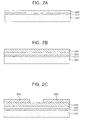
- FIGS. 2A to 2F are cross-sectional views illustrating a method of forming a polycrystalline silicon layer presented as another embodiment of the invention.
- buffer layer 210 is formed on transparent insulating substrate 200 such as glass or plastic.
- Buffer layer 210 inhibits moisture or impurities generated on the substrate from diffusing into a device to be formed on buffer layer 210, or enable a semiconductor layer to be well crystallized by regulating a heat transmission rate during crystallization.
- Amorphous silicon layer 220 is formed on buffer layer 210 by using PVD or CVD.
- second pattern layer 240 is formed to enable diffusion of a metal catalyst into amorphous silicon layer 220.
- Second pattern layer 240 includes a silicon nitride layer, and may have a thickness of about 50 ⁇ to 5,000 ⁇ .
- first pattern layer 230 is formed on second pattern layer 240.
- First pattern layer 230 has at least one opening to expose a predetermined region of second pattern layer 240.
- First pattern layer 230 includes a silicon oxide layer which does not diffuse a metal catalyst, and can have a thickness of about 50 ⁇ to 5,000 ⁇ .
- metal catalyst layer 250 is formed on the upper surfaces of first pattern layer 230 and the exposed region of second pattern layer 240.
- Metal catalyst layer 250 is formed of at least one of nickel (Ni), palladium (Pd), titanium (Ti), silver (Ag), gold (Au), aluminum (Al), tin (Sn), antimony (Sb), copper (Cu), cobalt (Co), molybdenum (Mo), chromium (Cr), ruthenium (Ru), rhodium (Rh), cadmium (Cd), and platinum (Pt).
- Metal catalyst 250 can be formed to have a concentration of 10 11 to 10 15 atoms/cm 2 .
- the extent of crystallization of amorphous silicon layer 220 varies depending on the concentration of metal catalyst layer 250. For example, when metal catalyst layer 250 is formed to have a very high concentration, a grain size of a polycrystalline silicon layer not only becomes finer, but an amount of a metal catalyst left on the polycrystalline silicon layer also increases, so that characteristics of the polycrystalline silicon layer deteriorate.
- metal catalyst layer 250 is formed to have a very low concentration, it is difficult to deposit the layer evenly by the use of a deposition apparatus, and a seed is not sufficiently formed to crystallize amorphous silicon layer 220.
- metal catalyst 260 in metal crystal layer 250 diffuses into a predetermined region of amorphous silicon layer 220 by heat-treating the substrate that includes amorphous silicon layer 220, first pattern layer 230, second pattern layer 240, the metal catalyst layer 250.
- the diffused metal catalyst forms a seed (not illustrated), and a predetermined region of amorphous silicon layer 220 is crystallized into seed region 270 by the seed.
- seed region 270 is affected by diffusion of the metal catalyst.
- Metal catalyst 260 diffuses easily into second pattern layer 240, but does not diffuse into first pattern layer 230, and thereby the seed region can be formed under the exposed region of second pattern layer 240. That is, a metal catalyst of metal catalyst layer 250, which is formed on first pattern layer 230, is not diffused, while the metal catalyst deposited on second pattern layer 240 easily diffuses to reach amorphous silicon layer 220.
- Grains of a polycrystalline silicon layer of seed region 270 radially grow around seeds forming a slightly irregular circular shape, and thereby each grain boundary has also a slightly irregular circular shape.
- a plurality of grains is formed in seed region 270, but position and the number of the seeds are not regulated. As a result, crystal growth directions are random in seed region 270, and thereby directions of grain boundaries are random in seed region 270 as well.
- a portion of amorphous silicon layer 220 under first pattern layer 230 is formed into crystallization region 290 by spread of the crystallinity of seed region 270.
- Crystallization region 290 is directly affected by seed region 270. That is, since crystallization region 290 is crystallized by the spread of crystallinity of seed region 270, crystalline size and the direction of the crystallization of crystallization region 290 is affected by the crystalline size and the direction of the crystallization of the seed region 270.
- the seed is not formed in crystallization region 290, unlike in seed region 270, so that the metal catalyst hardly exists there.
- Grain boundaries of crystallization region 290 are formed along the crystal growth direction 280 of crystallization region 290. That is, the major direction of the grain boundaries is perpendicular to the longitudinal direction of seed region 270. Crystallization of seed region 270 and crystallization region 290 is performed at a temperature of about 400 °C to 800 °C for 1 minutes to 3,000 minutes.
- FIGS. 3A and 3B are plan views of a polycrystalline silicon layer crystallized according to the method of the present invention.
- an amorphous silicon layer is crystallized into a polycrystalline silicon layer by the method described above with reference to FIGS. 1A to 1F or 2A to 2F.
- seed region 310 and crystallization region 320 are shown in FIGS. 3A and 3B.
- Seed region 310 is crystallized by the SGS crystallization technique, and crystallization region 320 is formed by causing the crystallinity of seed region 310 to spread.
- FIG. 3B which is an enlargement of region A of FIG. 3A, is divided into seed region 310 crystallized by the SGS crystallization technique, crystallization region 320 formed by the growth of crystals from seed region 310 and their interface 340.
- a plurality of polygonal (similar to a circular shape) grains 350 exist in seed region 310, and grain boundaries 360 are formed along a direction approximately perpendicular to the stretched direction of interface 340 in crystallization region 320.
- the stretched direction of interface 340 is defined as a longitudinal direction of the seed region.
- the direction of grain boundaries inside seed region 310 is random, while the major direction of grain boundaries in crystallization region 320 is regular and is approximately perpendicular to the stretched direction of interface 340.
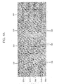
- FIG. 4A is a photograph showing seed regions 310 and crystallization regions 320
- FIG. 4B is a graph showing a relationship between an area of a seed region and growth length of a crystallization region according to the invention.
- width of a seed region is defined as a distance of the seed region along a direction perpendicular to a longitudinal (or stretched) direction of the seed region, as marked as W1-W4 in FIG. 4A.
- Length of a seed region is defined as a distance along the longitudinal direction of the seed region.
- lengths L of seed regions 310 is set to be 450 ⁇ m.
- width of the seed region varies depending on a location along the length L. If width W1 of seed region 310 is 100 ⁇ m, the growth length of crystallization region 330 is 100 ⁇ m or more, and if width W2 of seed region 310 is 50 ⁇ m, the growth length of crystallization region 330 is 100 ⁇ m or more. In other words, whenever width W1 and W2 of seed region 310 are more than 50 ⁇ m, the growth lengths of crystallization region are 100 ⁇ m or more. Thus, the crystallization region is almost saturated.
- width W3 of seed region 310 is 10 ⁇ m
- growth length 330 of crystallization region 320 is about 80 ⁇ m.
- the growth length of the crystallization region of the 10 ⁇ m-wide seed region increases around the region closer to the 50 ⁇ m-wide seed region. This is because the growth length of the crystallization region of the 10 ⁇ m-wide seed region is affected by the 50 ⁇ m-wide seed region.
- FIG. 4B roughly rectangle seed regions having a predetermined area were formed, and growth lengths of the crystallization region were measured in order to observe whether growth starts so as to form the crystallization region when the width of seed region 310 was between about 2 ⁇ m and 10 ⁇ m.
- the strategy was to observe whether growth is possible by forming square seed regions which have equal length and width.
- Another reason for forming the square seed regions is that it becomes more difficult to form first pattern layer 130, second pattern layer 140, and metal catalyst layer 150, described in FIGS. 1D to 1F and 2D to 2F, and to diffuse a metal catalyst from the metal catalyst layer, as the width of the seed region becomes narrower.
- a metal catalyst is easily diffused. This is because a metal catalyst is more easily diffused through a diffusion path with similar width and length than through a narrow width and large length.
- a growth length of a crystallization region is about 110 ⁇ m
- the area of the seed region is 4,900 ⁇ m 2 (if the length of the rectangular seed region is calculated in terms of 450 ⁇ m, its width is about 11 ⁇ m)
- the growth length of the crystallization region is about 100 ⁇ m.
- the widths corresponds to 8 ⁇ m, 5.5 ⁇ m, 3.5 ⁇ m, 0.8 ⁇ m, and 0.2 ⁇ m, respectively, and the growth lengths of the crystallization region are about 50 ⁇ m, 25 ⁇ m, 20 ⁇ m, 5 ⁇ m, and 0 ⁇ m, respectively as shown in the graph of FIG. 4B.
- the growth length is longer in the seed region with roughly the same length and width
- the seed regions having areas of 3600 ⁇ m 2 , 2500 ⁇ m 2 , 1600 ⁇ m 2 , 400 ⁇ m 2 , and 100 ⁇ m 2 are substituted with the seed region having widths of 8 ⁇ m, 5.5 ⁇ m, 3.5 ⁇ m, 0.8 ⁇ m, and 0.2 ⁇ m and a length of 450 ⁇ m
- the possibility of growth can be known, but the exact growth length of the seed region having a length of 450 ⁇ m cannot be known. Therefore, if a seed region with roughly the same length and width has an area of 1600 ⁇ m 2 , the growth length is 20 ⁇ m.
- FIG. 5 is a plan view of an organic electroluminescent device including a crystallized semiconductor layer
- FIGS. 6A to 6C show embodiments of crystallizing the semiconductor layer in FIG. 5.
- the device includes an unit pixel defined by scan line 410, data line 420, and common power line 430 disposed on a transparent insulating substrate such as glass or plastic.
- the unit pixel includes thin film transistor 440 having semiconductor layer 441, gate insulating layer (not shown) disposed on semiconductor layer 441, gate electrode 442 disposed on the gate insulating layer and corresponding to semiconductor layer 441, and source and drain electrodes 443 connected to predetermined regions of semiconductor layer 441, capacitor 450 including lower and upper electrodes 451 and 452, first electrode 460 connected to the source and drain electrodes of the thin film transistor, an organic film layer (not shown) disposed on first electrode 460 and including at least an organic emission layer, and a second electrode (not shown) disposed on the organic film layer.
- Thin film transistor 440 can be formed of a semiconductor layer formed by patterning a crystallization region crystallized using the technique shown in FIGS. 1A to 1F or 2A to 2F.
- FIGS. 6A to 6C illustrate region 470 to be formed as the seed region and a growth direction of a crystallization region 480.
- a semiconductor layer is formed by forming an amorphous silicon layer on a substrate, by crystallizing the amorphous silicon layer with the technique described referring to FIGS. 1A to 1F or 2A to 2F, and by patterning the amorphous silicon layer. That is, FIG. 6A shows the crystallization of a semiconductor layer as follows.
- a region to be formed as a seed region is disposed in parallel with data line 420 or common power line 430, which will be formed in later processes. Crystallization region is formed by growing grains from the seed region, and then is patterned, thereby forming semiconductor region 441.
- FIG. 6B shows the crystallization of a semiconductor layer in another configuration as follows.
- a region to be formed as a seed region is disposed parallel to scan line 410, which will be formed in later processes.
- a crystallization region is formed by growing grains perpendicularly to a longitudinal direction of the seed region, and then is patterned, thereby forming semiconductor region 441.
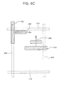
- FIG. 6C illustrates another method of the crystallization of a semiconductor layer, which is performed the methods described referring to FIGS. 6A and 6B at the same time.
- a crystallization region is grown from a seed region formed parallel to data line 420 or common power line 430, and is patterned to form a semiconductor layer shown in the upper left corner of FIG. 6C.
- Another crystallization region is grown from a seed region formed parallel to scan line 410, and is patterned to form a semiconductor layer shown in the right side of FIG. 6C. Therefore, one semiconductor layer is obtained with the same method used to obtain the semiconductor layer shown in FIG. 6A, in which the grain boundaries are formed parallel to scan line 410.
- the direction parallel to scan line 410 is a travelling direction of electric charges, and the charges have a high travelling speed.
- Another semiconductor layer is obtained with the same method used to obtain the semiconductor layer shown in FIG. 6B, in which the grain boundaries are formed perpendicular to scan line 410. In this case, the grain boundaries are formed perpendicular to the travelling direction of electric charges. Therefore the travelling speed of the charges is low compared to the semiconductor layer formed in the method described referring to FIG. 6A, but has a high uniformity.
- the semiconductor layer shown in FIG. 6C it is possible to form the semiconductor layer to have required characteristics. That is, a semiconductor layer of a switching thin film transistor can be obtained, in which grain boundaries are disposed along a travelling direction of electric charges, and charges have a high travelling speed. Alternatively, another semiconductor layer of a driving thin film transistor can be obtained, in which grain boundaries are disposed perpendicular to the travelling direction of electric charges, and uniformity of another semiconductor layers is excellent.
- FIGS. 7A and 7B shows seed regions formed in different shapes from the shapes shown in FIGS. 6A to 6C.
- the seed regions illustrated in FIGS. 6A to 6C are formed in a line shape because it is easy to dispose first and second pattern layers.
- the seed region can be formed into a bent line shape 470a or curve 470b.
- the seed region applicable to the present invention can be formed in any shape but its smallest dimension is 3.5 ⁇ m.
- the polycrystalline silicon layer, a flat panel display made with the polycrystalline silicon layer, and a method of fabricating both according to the present invention enable fabrication of a thin film transistor and a flat panel display with excellent characteristics and uniformity.
- the predetermined region of the amorphous silicon layer is crystallized with the SGS crystallization technique. Regions other than the predetermined region are crystallized by spreading the crystallinity to the amorphous silicon layer.
- the semiconductor layer is formed by the grown amorphous silicon layer.
Landscapes
- Engineering & Computer Science (AREA)
- Manufacturing & Machinery (AREA)
- Recrystallisation Techniques (AREA)
- Thin Film Transistor (AREA)
Abstract
Description
- The present invention relates to a polycrystalline silicon layer, a flat panel display using the same, and a method of fabricating the same, and more particularly, to a polycrystalline silicon layer, a flat panel display using the same, and a method of fabricating the same in which a predetermined region of an amorphous silicon layer is crystallized by a super grain silicon (SGS) crystallization technique, crystallinity of a seed region is spread to become a crystallization layer, and then the crystallization layer is formed as a semiconductor layer. The resulting polycrystalline silicon layer has excellent characteristics and uniformity.
- A thin film transistor used in a flat panel display, such as an organic electro luminescence device, is made by depositing an amorphous silicon layer on a transparent substrate such as a glass, quartz or plastic substrate, dehydrogenating the amorphous silicon layer, ion-implanting impurities for forming a channel, crystallizing the amorphous silicon layer to form a polycrystalline silicon layer, and then patterning the polycrystalline silicon layer to fabricate a semiconductor layer.
- Methods of crystallizing the amorphous silicon layer into a polycrystalline silicon layer include solid phase crystallization (SPC), excimer laser crystallization (ELC), metal induced crystallization (MIC), and metal induced lateral crystallization (MILC). SPC is a method of annealing an amorphous silicon layer for several to several tens of hours at a temperature of about 700 °C or less, which is a transition temperature of glass used as a substrate of a display device employing a thin film transistor. ELC is a method of crystallizing a silicon layer by irradiating the silicon layer with an excimer laser and locally heating the silicon layer to a high temperature for very short time, and MIC is a method of using phase transfer induction from amorphous silicon to polysilicon by contacting the amorphous silicon layer with metals such as nickel (Ni), palladium (Pd), gold (Au), and aluminum (Al), or implanting such metals into the amorphous silicon layer. MILC involves a technique of inducing sequential crystallization of silicon by lateral diffusion of silicide formed by reacting metal with the silicon.
- However, when thin film transistors are made of the polycrystalline silicon layers crystallized by these methods, the thin film transistors have non-uniform characteristics such as non-uniform threshold voltage and off-characteristics due to non-uniform grain size and irregular distribution of grain boundaries.
- The present invention seeks to provide a polycrystalline silicon layer with superior characteristics obtained by crystallizing a seed region through a super grain silicon (SGS) technique, and by spreading the crystallinity of the seed region to a crystallization region where the thin film transistor will be formed. A semiconductor layer fabricated by the method of the present invention has a uniform grain size and a regular distribution of grain boundaries. The present invention also provides a flat panel display incorporated using the polycrystalline silicon layer.
- One aspect of the invention provides a polycrystalline silicon layer as set out in
Claim 1. Preferred features of this aspect of the invention are set out in Claims 2 to 10. - Another aspect of the invention provides a method of fabricating a polycrystalline silicon layer as set out in Claim 11. Preferred features of this aspect of the invention are set out in Claims 12 to 20.
- Yet another aspect of the invention provides a flat panel display as set out in Claim 21. Preferred features of this aspect of the invention are set out in Claims 22 and 23.
- A more complete appreciation of the invention, and many of the attendant advantages thereof, will be readily apparent as the same becomes better understood by reference to the following detailed description of embodiments thereof when considered in conjunction with the accompanying drawings in which like reference symbols indicate the same or similar components wherein:
- FIGS. 1A to 1F are cross-sectional views illustrating a method of forming a polycrystalline silicon layer presented as an embodiment of the invention;
- FIGS. 2A to 2F are cross-sectional views illustrating a method of forming a polycrystalline silicon layer presented as another embodiment of the invention;
- FIGS. 3A and 3B are plan views showing a polycrystalline silicon layer crystallized according to the method presented as another embodiment of the present invention;
- FIGS. 4A and 4B are a photograph and a graph which show a relationship between a width of a seed region and a growth length of a crystallization region according to another embodiment of the invention;
- FIG. 5 is a plan view of an organic electro luminescent device including a crystallized semiconductor layer;
- FIGS. 6A to 6C are examples showing crystallization of the semiconductor layer of FIG. 5; and
- FIGS. 7A and 7B show shapes of a seed region.
- The present invention will now be described more completely hereinafter with reference to the accompanying drawings, in which embodiments of the invention are shown. These embodiments are provided to make this disclosure thorough and complete. In the drawings, the thickness and length of layers and regions may be exaggerated for clarity. Like elements are denoted by like reference numerals throughout the drawings.
- FIGS. 1A to 1F are cross-sectional views illustrating a method of forming a polycrystalline silicon layer presented as an embodiment of the invention. Referring to FIG. 1A,
buffer layer 110 is formed on transparentinsulating substrate 100 such as glass or plastic substrate. Here,buffer layer 110 serves to inhibit moisture or impurities generated on the substrate from diffusing into a device that is to be formed onbuffer layer 110, and to regulate a heat transmission rate during crystallization, thereby enabling a semiconductor layer to be smoothly crystallized.Amorphous silicon layer 120 is formed onbuffer layer 110 using physical vapor deposition (PVD) or chemical vapor deposition (CVD). - Referring to FIG. 1B,
first pattern layer 130 having a silicon oxide layer, which is not able to diffuse a metal catalyst, is formed onamorphous silicon layer 120. Here,first pattern layer 130 has at least one opening to expose a predetermined region ofamorphous silicon layer 120.First pattern layer 130 can be formed to a thickness of about 50 Å to about 5,000 Å. - Referring to FIG. 1C,
second pattern layer 140 is formed on the entire surface of the substrate coveringfirst pattern layer 130 and exposed region ofamorphous silicon layer 120. Here,second pattern layer 140 includes a silicon nitride layer to enable diffusion of the metal catalyst, and may have a thickness of about 50 Å to about 5,000 Å. Moreover,second pattern layer 140 should be formed to entirely cover the region ofamorphous silicon layer 120 exposed byfirst pattern layer 130. - Referring to FIG. 1D,
metal catalyst layer 150 is formed onsecond pattern layer 140. Here,metal catalyst layer 150 is made of one of nickel (Ni), palladium (Pd), titanium (Ti), silver (Ag), gold (Au), aluminum (Al), tin (Sn), antimony (Sb), copper (Cu), cobalt (Co), molybdenum (Mo), chromium (Cr), ruthenium (Ru), rhodium (Rh), cadmium (Cd), and platinum (Pt). -
Metal catalyst layer 150 may be formed at a concentration of 1011 to 1015 atoms/cm2. The extent of the crystallization ofamorphous silicon layer 120 varies depending on the concentration ofmetal catalyst layer 150. For example, whenmetal catalyst layer 150 is formed to have a very high concentration, a grain size of a polycrystalline silicon layer not only becomes finer, but an amount of a metal catalyst left on the polycrystalline silicon layer also increases. Therefore, characteristics of the polycrystalline silicon layer deteriorate. On the other hand, whenmetal catalyst layer 150 is formed to have a very low concentration, it is difficult to deposit the layer evenly with a deposition apparatus, and a seed is not sufficiently formed to crystallizeamorphous silicon layer 120. - Referring to FIG. 1E, the metal catalyst in
metal catalyst layer 150 is diffused into a predetermined region ofamorphous silicon layer 120 by heat-treating the substrate that includesamorphous silicon layer 120,first pattern layer 130,second pattern layer 140, andmetal catalyst layer 150. A seed (not illustrated) is formed by the diffused metal catalyst, so that the predetermined region ofamorphous silicon layer 120 is crystallized into aseed region 170. - The formation of
seed region 170 is affected by diffusion ofmetal catalyst 160. In order to form the seed region, the metal catalyst is easily diffused intosecond pattern layer 140, but is not diffused intofirst pattern layer 130. - The metal catalyst in
metal catalyst layer 150 is diffused intoamorphous silicon layer 120 by heat-treating the substrate, so that the seed is formed. Accordingly, the metal catalyst remains inseed region 170 after crystallization, and has a concentration of 1×10¹³ atoms/cm2 or less. -
Seed region 170 is a polycrystalline silicon layer crystallized by the super grain silicon (SGS) crystallization technique. Here, the SGS crystallization technique includes the steps of sequentially stacking the amorphous silicon layer and the second pattern layer enabling diffusion of the metal catalyst from the metal catalyst layer on the substrate, diffusing the metal catalyst into the amorphous silicon layer through the second pattern layer by heat-treating the substrate, forming a seed, and crystallizing the amorphous silicon layer by the seed. - Grains of the polycrystalline silicon layer of
seed region 170 radially grow around the seeds forming a slightly irregular circular shape, and thereby each grain boundary also has a slightly irregular circular shape. The plurality of grains are formed inseed region 170, but positions and the number of the seeds are not regulated. As a result, growth directions of crystals are random inseed region 170, and thereby directions of grain boundaries are random inseed region 170 as well. - Referring to FIG. 1F, portion of
amorphous silicon layer 120 that is located underfirst pattern layer 130 is formed intocrystallization region 190 by spreading the crystallinity ofseed region 170 intocrystallization region 190. In other words, the crystallinity ofseed region 170 spreads beyondseed region 170.Crystallization region 190 is directly affected byseed region 170. That is,crystallization region 190 is grown by the spread of the crystallinity ofseed region 170, and therefore a crystalline size and a crystallization direction ofcrystallization region 190 is affected by the crystalline size and the crystallization direction ofseed region 170. However, the seed is not formed incrystallization region 190, unlike inseed region 170, so that the metal catalyst hardly exists there. - Grain boundaries of
crystallization region 190 are formed alongcrystal growth direction 180 ofcrystallization region 190 as a major direction. That is, the major direction of the grain boundaries is perpendicular to the longitudinal direction ofseed region 170. Crystallization ofseed region 170 andcrystallization region 190 is performed at a temperature of about 400 °C to 800 °C for 1 minute to 3,000 minutes. - FIGS. 2A to 2F are cross-sectional views illustrating a method of forming a polycrystalline silicon layer presented as another embodiment of the invention. Referring to FIG. 2A,
buffer layer 210 is formed on transparent insulatingsubstrate 200 such as glass or plastic.Buffer layer 210 inhibits moisture or impurities generated on the substrate from diffusing into a device to be formed onbuffer layer 210, or enable a semiconductor layer to be well crystallized by regulating a heat transmission rate during crystallization.Amorphous silicon layer 220 is formed onbuffer layer 210 by using PVD or CVD. - Referring to FIG. 2B,
second pattern layer 240 is formed to enable diffusion of a metal catalyst intoamorphous silicon layer 220.Second pattern layer 240 includes a silicon nitride layer, and may have a thickness of about 50 Å to 5,000 Å. - Referring to FIG. 2C,
first pattern layer 230 is formed onsecond pattern layer 240.First pattern layer 230 has at least one opening to expose a predetermined region ofsecond pattern layer 240.First pattern layer 230 includes a silicon oxide layer which does not diffuse a metal catalyst, and can have a thickness of about 50 Å to 5,000 Å. - Referring to FIG. 2D,
metal catalyst layer 250 is formed on the upper surfaces offirst pattern layer 230 and the exposed region ofsecond pattern layer 240.Metal catalyst layer 250 is formed of at least one of nickel (Ni), palladium (Pd), titanium (Ti), silver (Ag), gold (Au), aluminum (Al), tin (Sn), antimony (Sb), copper (Cu), cobalt (Co), molybdenum (Mo), chromium (Cr), ruthenium (Ru), rhodium (Rh), cadmium (Cd), and platinum (Pt). -
Metal catalyst 250 can be formed to have a concentration of 1011 to 1015 atoms/cm2. The extent of crystallization ofamorphous silicon layer 220 varies depending on the concentration ofmetal catalyst layer 250. For example, whenmetal catalyst layer 250 is formed to have a very high concentration, a grain size of a polycrystalline silicon layer not only becomes finer, but an amount of a metal catalyst left on the polycrystalline silicon layer also increases, so that characteristics of the polycrystalline silicon layer deteriorate. Whenmetal catalyst layer 250 is formed to have a very low concentration, it is difficult to deposit the layer evenly by the use of a deposition apparatus, and a seed is not sufficiently formed to crystallizeamorphous silicon layer 220. - Referring to FIG. 2E,
metal catalyst 260 inmetal crystal layer 250 diffuses into a predetermined region ofamorphous silicon layer 220 by heat-treating the substrate that includesamorphous silicon layer 220,first pattern layer 230,second pattern layer 240, themetal catalyst layer 250. The diffused metal catalyst forms a seed (not illustrated), and a predetermined region ofamorphous silicon layer 220 is crystallized intoseed region 270 by the seed. - The formation of
seed region 270 is affected by diffusion of the metal catalyst.Metal catalyst 260 diffuses easily intosecond pattern layer 240, but does not diffuse intofirst pattern layer 230, and thereby the seed region can be formed under the exposed region ofsecond pattern layer 240. That is, a metal catalyst ofmetal catalyst layer 250, which is formed onfirst pattern layer 230, is not diffused, while the metal catalyst deposited onsecond pattern layer 240 easily diffuses to reachamorphous silicon layer 220. - Grains of a polycrystalline silicon layer of
seed region 270 radially grow around seeds forming a slightly irregular circular shape, and thereby each grain boundary has also a slightly irregular circular shape. A plurality of grains is formed inseed region 270, but position and the number of the seeds are not regulated. As a result, crystal growth directions are random inseed region 270, and thereby directions of grain boundaries are random inseed region 270 as well. - Referring to FIG. 2F, a portion of
amorphous silicon layer 220 underfirst pattern layer 230 is formed intocrystallization region 290 by spread of the crystallinity ofseed region 270.Crystallization region 290 is directly affected byseed region 270. That is, sincecrystallization region 290 is crystallized by the spread of crystallinity ofseed region 270, crystalline size and the direction of the crystallization ofcrystallization region 290 is affected by the crystalline size and the direction of the crystallization of theseed region 270. However, the seed is not formed incrystallization region 290, unlike inseed region 270, so that the metal catalyst hardly exists there. - Grain boundaries of
crystallization region 290 are formed along thecrystal growth direction 280 ofcrystallization region 290. That is, the major direction of the grain boundaries is perpendicular to the longitudinal direction ofseed region 270. Crystallization ofseed region 270 andcrystallization region 290 is performed at a temperature of about 400 °C to 800 °C for 1 minutes to 3,000 minutes. - FIGS. 3A and 3B are plan views of a polycrystalline silicon layer crystallized according to the method of the present invention. Referring to FIG. 3A, an amorphous silicon layer is crystallized into a polycrystalline silicon layer by the method described above with reference to FIGS. 1A to 1F or 2A to 2F. When a metal catalyst layer, a first pattern layer, and a second pattern layer are removed,
seed region 310 andcrystallization region 320 are shown in FIGS. 3A and 3B.Seed region 310 is crystallized by the SGS crystallization technique, andcrystallization region 320 is formed by causing the crystallinity ofseed region 310 to spread. - FIG. 3B, which is an enlargement of region A of FIG. 3A, is divided into
seed region 310 crystallized by the SGS crystallization technique,crystallization region 320 formed by the growth of crystals fromseed region 310 and theirinterface 340. A plurality of polygonal (similar to a circular shape)grains 350 exist inseed region 310, andgrain boundaries 360 are formed along a direction approximately perpendicular to the stretched direction ofinterface 340 incrystallization region 320. The stretched direction ofinterface 340 is defined as a longitudinal direction of the seed region. The direction of grain boundaries insideseed region 310 is random, while the major direction of grain boundaries incrystallization region 320 is regular and is approximately perpendicular to the stretched direction ofinterface 340. - FIG. 4A is a photograph showing
seed regions 310 andcrystallization regions 320, and FIG. 4B is a graph showing a relationship between an area of a seed region and growth length of a crystallization region according to the invention. Referring to FIGS. 4A and 4B, it is shown that the growth length of the crystallization region depends on the width of the seed region at a given length of the seed region. Herein width of a seed region is defined as a distance of the seed region along a direction perpendicular to a longitudinal (or stretched) direction of the seed region, as marked as W1-W4 in FIG. 4A. Length of a seed region is defined as a distance along the longitudinal direction of the seed region. - In order to obtain the relationship between an area of a seed region and growth length of a crystallization region, lengths L of
seed regions 310 is set to be 450 µm. As shown in FIG. 4A, width of the seed region varies depending on a location along the length L. If width W1 ofseed region 310 is 100 µm, the growth length ofcrystallization region 330 is 100 µm or more, and if width W2 ofseed region 310 is 50 µm, the growth length ofcrystallization region 330 is 100 µm or more. In other words, whenever width W1 and W2 ofseed region 310 are more than 50 µm, the growth lengths of crystallization region are 100 µm or more. Thus, the crystallization region is almost saturated. - If width W3 of
seed region 310 is 10 µm,growth length 330 ofcrystallization region 320 is about 80 µm. The growth length of the crystallization region of the 10 µm-wide seed region, however, increases around the region closer to the 50 µm-wide seed region. This is because the growth length of the crystallization region of the 10 µm-wide seed region is affected by the 50 µm-wide seed region. - In the view of the result shown in FIG. 4A, only when
seed region 310 is at least 10 µm wide, does growth start so as to formcrystallization region 330. Accordingly, it can be understood that if the seed region is 2 µm wide or less, growth does not start andcrystallization region 330 is not formed. However, it cannot be seen from the result of FIG. 4A alone whether growth starts or not in the case thatseed region 310 is between about 2 µm and 10 µm wide. - Referring to FIG. 4B, roughly rectangle seed regions having a predetermined area were formed, and growth lengths of the crystallization region were measured in order to observe whether growth starts so as to form the crystallization region when the width of
seed region 310 was between about 2 µm and 10 µm.
As it is difficult to make aseed region 450 µm long and several µm wide, the strategy was to observe whether growth is possible by forming square seed regions which have equal length and width. Another reason for forming the square seed regions is that it becomes more difficult to formfirst pattern layer 130,second pattern layer 140, andmetal catalyst layer 150, described in FIGS. 1D to 1F and 2D to 2F, and to diffuse a metal catalyst from the metal catalyst layer, as the width of the seed region becomes narrower. When a rectangular seed region has substantially the same length and width by patterning the first pattern layer or the second pattern layer into a predetermined shape, a metal catalyst is easily diffused. This is because a metal catalyst is more easily diffused through a diffusion path with similar width and length than through a narrow width and large length. - Referring to FIG. 4B, when the rectangular seed region has an area of 6400 µm2 (if the rectangular seed region is calculated in terms of a length of 450 µm, its width is about 14 µm), a growth length of a crystallization region is about 110 µm, and when the area of the seed region is 4,900 µm2 (if the length of the rectangular seed region is calculated in terms of 450 µm, its width is about 11 µm), the growth length of the crystallization region is about 100 µm. In addition, when the areas of the seed region are 3600 µm2, 2500 µm2, 1600 µm2, 400 µm2, and 100 µm2, the widths corresponds to 8 µm, 5.5 µm, 3.5 µm, 0.8 µm, and 0.2 µm, respectively, and the growth lengths of the crystallization region are about 50 µm, 25 µm, 20 µm, 5 µm, and 0 µm, respectively as shown in the graph of FIG. 4B.
- Comparing the results of FIGS. 4A with the results of FIG. 4B, it can be shown that the case of having an area of 4900 µm2 in FIG. 4B is similar to the case of having a width of 10 µm in FIG. 4A, but the growth lengths are 100 µm and 80 µm, respectively. In other words, the growth length obtained from a seed region with roughly the same length and width is slightly different from the growth length obtained from a seed region which has a greater length and a narrower width even though the areas of the seed regions are approximately the same.
- Thus, considering that the growth length is longer in the seed region with roughly the same length and width, when the seed regions having areas of 3600 µm2, 2500 µm2, 1600 µm2, 400 µm2, and 100 µm2 are substituted with the seed region having widths of 8 µm, 5.5 µm, 3.5 µm, 0.8 µm, and 0.2 µm and a length of 450 µm, the possibility of growth can be known, but the exact growth length of the seed region having a length of 450 µm cannot be known. Therefore, if a seed region with roughly the same length and width has an area of 1600 µm2, the growth length is 20 µm. Considering the longer growth length in a rough square seed region, it can be known that growth is possible when a width is 3.5 µm. Meanwhile, if a rectangle with roughly the same length and width has an area of 400 µm2, the growth length is 5 µm, and thus it can be concluded that crystallization hardly occurs when a width is 0.8 µm. As a result, if the seed region is not nearly square, but a rectangle that has a big difference between the length and the width (the length of the rectangle is 450 µm), growth is possible when the seed region has a width of at least 3.5 µm.
- FIG. 5 is a plan view of an organic electroluminescent device including a crystallized semiconductor layer, and FIGS. 6A to 6C show embodiments of crystallizing the semiconductor layer in FIG. 5. Referring to FIG. 5, the device includes an unit pixel defined by
scan line 410,data line 420, andcommon power line 430 disposed on a transparent insulating substrate such as glass or plastic. The unit pixel includesthin film transistor 440 havingsemiconductor layer 441, gate insulating layer (not shown) disposed onsemiconductor layer 441,gate electrode 442 disposed on the gate insulating layer and corresponding tosemiconductor layer 441, and source and drainelectrodes 443 connected to predetermined regions ofsemiconductor layer 441,capacitor 450 including lower andupper electrodes first electrode 460 connected to the source and drain electrodes of the thin film transistor, an organic film layer (not shown) disposed onfirst electrode 460 and including at least an organic emission layer, and a second electrode (not shown) disposed on the organic film layer. - An interlayer insulating layer (not shown) and/or a planarization layer is disposed on source and drain
electrodes 443 to electrically protect and planarizethin film transistor 440.Thin film transistor 440 can be formed of a semiconductor layer formed by patterning a crystallization region crystallized using the technique shown in FIGS. 1A to 1F or 2A to 2F. - FIGS. 6A to 6C illustrate
region 470 to be formed as the seed region and a growth direction of acrystallization region 480. A semiconductor layer is formed by forming an amorphous silicon layer on a substrate, by crystallizing the amorphous silicon layer with the technique described referring to FIGS. 1A to 1F or 2A to 2F, and by patterning the amorphous silicon layer. That is, FIG. 6A shows the crystallization of a semiconductor layer as follows. A region to be formed as a seed region is disposed in parallel withdata line 420 orcommon power line 430, which will be formed in later processes. Crystallization region is formed by growing grains from the seed region, and then is patterned, thereby formingsemiconductor region 441. - FIG. 6B shows the crystallization of a semiconductor layer in another configuration as follows. A region to be formed as a seed region is disposed parallel to scan
line 410, which will be formed in later processes. A crystallization region is formed by growing grains perpendicularly to a longitudinal direction of the seed region, and then is patterned, thereby formingsemiconductor region 441. - FIG. 6C illustrates another method of the crystallization of a semiconductor layer, which is performed the methods described referring to FIGS. 6A and 6B at the same time. A crystallization region is grown from a seed region formed parallel to
data line 420 orcommon power line 430, and is patterned to form a semiconductor layer shown in the upper left corner of FIG. 6C. Another crystallization region is grown from a seed region formed parallel to scanline 410, and is patterned to form a semiconductor layer shown in the right side of FIG. 6C. Therefore, one semiconductor layer is obtained with the same method used to obtain the semiconductor layer shown in FIG. 6A, in which the grain boundaries are formed parallel to scanline 410. The direction parallel to scanline 410 is a travelling direction of electric charges, and the charges have a high travelling speed. Another semiconductor layer is obtained with the same method used to obtain the semiconductor layer shown in FIG. 6B, in which the grain boundaries are formed perpendicular to scanline 410. In this case, the grain boundaries are formed perpendicular to the travelling direction of electric charges. Therefore the travelling speed of the charges is low compared to the semiconductor layer formed in the method described referring to FIG. 6A, but has a high uniformity. - In the case of the semiconductor layer shown in FIG. 6C, it is possible to form the semiconductor layer to have required characteristics. That is, a semiconductor layer of a switching thin film transistor can be obtained, in which grain boundaries are disposed along a travelling direction of electric charges, and charges have a high travelling speed. Alternatively, another semiconductor layer of a driving thin film transistor can be obtained, in which grain boundaries are disposed perpendicular to the travelling direction of electric charges, and uniformity of another semiconductor layers is excellent.
- FIGS. 7A and 7B shows seed regions formed in different shapes from the shapes shown in FIGS. 6A to 6C. The seed regions illustrated in FIGS. 6A to 6C are formed in a line shape because it is easy to dispose first and second pattern layers. However, depending on the positions of the semiconductor layer or manufacture processes, the seed region can be formed into a
bent line shape 470a orcurve 470b. As a result, the seed region applicable to the present invention can be formed in any shape but its smallest dimension is 3.5 µm. - Consequently, the polycrystalline silicon layer, a flat panel display made with the polycrystalline silicon layer, and a method of fabricating both according to the present invention enable fabrication of a thin film transistor and a flat panel display with excellent characteristics and uniformity. The predetermined region of the amorphous silicon layer is crystallized with the SGS crystallization technique. Regions other than the predetermined region are crystallized by spreading the crystallinity to the amorphous silicon layer. The semiconductor layer is formed by the grown amorphous silicon layer.
- While embodiments of the present invention have been described herein by way of example, it will be apparent to those of ordinary skill in the art that various modifications in form and details can be made to the described embodiments without departing from the scope of the present invention as defined by the appended claims.
Claims (23)
- A polycrystalline silicon layer, comprising:a substrate;a seed region formed on the substrate, the seed region having at least 3.5 micro metres in width; anda crystallization region grown by the seed region and formed on the substrate.
- A polycrystalline silicon layer according to Claim 1, wherein the seed region has been crystallized by a super grain silicon (SGS) crystallization technique.
- A polycrystalline silicon layer according to Claim 1 or 2, wherein the crystallization region has been formed by spread of crystallinity of the seed region.
- A polycrystalline silicon layer according to any preceding Claim, wherein the seed region is formed in a line shape with a longer length than width.
- A polycrystalline silicon layer according to any preceding Claim, wherein the seed region includes at least one seed.
- A polycrystalline silicon layer according to Claim 5, wherein the seed includes at least one metal catalyst.
- A polycrystalline silicon layer according to Claim 6, wherein the metal catalyst has a concentration of 1×10¹³ atoms/cm2 or less.
- A polycrystalline silicon layer according to any preceding Claim, wherein the seed region has a width of 50 micro metres or less.
- A polycrystalline silicon layer according to any preceding Claim, wherein the seed region has at least one grain boundary, a direction of the grain boundary being random.
- A polycrystalline silicon layer according to any one of Claims 1 to 8, wherein a major direction of grain boundaries of the crystallization region is substantially perpendicular to a longitudinal direction of the seed region.
- A method of fabricating a polycrystalline silicon layer, comprising:forming an amorphous silicon layer on a substrate;forming a first pattern layer over the amorphous silicon layer, the first pattern layer having an opening through which a portion of the amorphous silicon layer is exposed;forming a second pattern layer over the amorphous silicon layer;forming a metal catalyst layer on the second pattern layer;crystallizing a region of the amorphous silicon layer to form a seed region in the amorphous silicon layer, the seed region having a width of at least 3.5 micro metres, the seed region being formed within the exposed portion of the amorphous silicon layer; andspreading crystallinity of the seed region beyond the exposed portion of the amorphous silicon layer.
- A method according to Claim 11, wherein the second pattern layer is formed over the first pattern layer and the second pattern layer contacts the amorphous layer via the opening.
- A method according to Claim 11, wherein the first pattern layer is formed over the second pattern layer and the said metal catalyst layer accesses the said second pattern layer via the opening.
- A method according to Claim 11, 12 or 13, wherein both of the step of crystallizing a region of the amorphous silicon layer and the step of spreading crystallinity of the seed region are performed by heat-treating the substrate.
- A method according to Claim 14, wherein heat-treating the substrate is performed at a temperature of about 400 °C to 800 °C for about 1 minute to 3,000 minutes.
- A method according to one of Claims 11 to 15, wherein the first pattern layer includes a silicon oxide layer.
- A method according to one of Claims 11 to 16, wherein the second pattern layer includes a silicon nitride layer.
- A method according to Claim 16 or 17, wherein the silicon oxide layer has a thickness of about 50Å to 5,000Å.
- A method according to Claim 17 or 18, wherein the silicon nitride layer has a thickness of about 50Å to 5000Å.
- A method according to one of Claims 11 to 19, wherein the metal catalyst layer includes a metal catalyst in a concentration of about 1011 atoms/cm2 to 1015 atoms/cm2.
- A flat panel display, comprising:a substrate;a semiconductor layer which is either parallel to or perpendicular to a major direction of the grain boundaries of a crystallization region grown from a seed region having at least 3.5 micro metres in width, the semiconductor layer being arranged on the substrate and formed by patterning the crystallization region;a gate insulating layer disposed on the semiconductor layer;a gate electrode disposed on the gate insulating layer;an interlayer insulating layer disposed on the gate electrode; anda source electrode and a drain electrode disposed on the interlayer insulating layer and contacting the semiconductor layer.
- A flat panel display according to Claim 21, further comprising:a first electrode connected to the source electrode or the drain electrode.
- A flat panel display according to Claim 21 or 22, wherein the seed region has been crystallized by a super grain silicon (SGS) crystallization technique, and the grain boundary formed by spread of crystallinity of the seed region.
Applications Claiming Priority (1)
| Application Number | Priority Date | Filing Date | Title |
|---|---|---|---|
| KR1020050122628A KR100721957B1 (en) | 2005-12-13 | 2005-12-13 | Polycrystalline silicon layer, flat panel display device using the polycrystalline silicon layer and method of manufacturing the same |
Publications (2)
| Publication Number | Publication Date |
|---|---|
| EP1798760A2 true EP1798760A2 (en) | 2007-06-20 |
| EP1798760A3 EP1798760A3 (en) | 2011-01-12 |
Family
ID=37913134
Family Applications (1)
| Application Number | Title | Priority Date | Filing Date |
|---|---|---|---|
| EP06256355A Ceased EP1798760A3 (en) | 2005-12-13 | 2006-12-13 | Polycrystalline silcon layer, flat panel display using the same, and method of fabricating the same. |
Country Status (5)
| Country | Link |
|---|---|
| US (1) | US8125033B2 (en) |
| EP (1) | EP1798760A3 (en) |
| JP (1) | JP5084241B2 (en) |
| KR (1) | KR100721957B1 (en) |
| CN (1) | CN1983571B (en) |
Cited By (1)
| Publication number | Priority date | Publication date | Assignee | Title |
|---|---|---|---|---|
| US9859454B2 (en) | 2010-02-11 | 2018-01-02 | Semiconductor Energy Laboratory Co., Ltd. | Photoelectric conversion device and fabrication method thereof |
Families Citing this family (2)
| Publication number | Priority date | Publication date | Assignee | Title |
|---|---|---|---|---|
| US8035185B2 (en) * | 2003-03-26 | 2011-10-11 | Sony Corporation | Electrode, method of making same, photoelectric transfer element, method of manufacturing same, electronic device and method of manufacturing same |
| CN113454792A (en) * | 2018-12-27 | 2021-09-28 | 深圳市柔宇科技股份有限公司 | Functional device and manufacturing method thereof |
Citations (2)
| Publication number | Priority date | Publication date | Assignee | Title |
|---|---|---|---|---|
| US20030010980A1 (en) * | 2001-07-10 | 2003-01-16 | Semiconductor Energy Laboratory Co., Ltd. | Semiconductor device and method for manufacturing same |
| US6744069B1 (en) * | 1996-01-19 | 2004-06-01 | Semiconductor Energy Laboratory Co., Ltd. | Semiconductor device and its manufacturing method |
Family Cites Families (27)
| Publication number | Priority date | Publication date | Assignee | Title |
|---|---|---|---|---|
| US5498573A (en) * | 1989-11-29 | 1996-03-12 | General Electric Company | Method of making multi-layer address lines for amorphous silicon liquid crystal display devices |
| JPH0766424A (en) * | 1993-08-20 | 1995-03-10 | Semiconductor Energy Lab Co Ltd | Semiconductor device and manufacturing method thereof |
| TW272319B (en) * | 1993-12-20 | 1996-03-11 | Sharp Kk | |
| US6162667A (en) * | 1994-03-28 | 2000-12-19 | Sharp Kabushiki Kaisha | Method for fabricating thin film transistors |
| JP3621151B2 (en) * | 1994-06-02 | 2005-02-16 | 株式会社半導体エネルギー研究所 | Method for manufacturing semiconductor device |
| JP3504336B2 (en) * | 1994-06-15 | 2004-03-08 | 株式会社半導体エネルギー研究所 | Method for manufacturing semiconductor device |
| JP3662479B2 (en) * | 1994-06-22 | 2005-06-22 | 株式会社半導体エネルギー研究所 | Method for manufacturing semiconductor device |
| TW280943B (en) * | 1994-07-15 | 1996-07-11 | Sharp Kk | |
| JP3124480B2 (en) * | 1995-12-12 | 2001-01-15 | 株式会社半導体エネルギー研究所 | Method for manufacturing semiconductor device |
| US6555449B1 (en) * | 1996-05-28 | 2003-04-29 | Trustees Of Columbia University In The City Of New York | Methods for producing uniform large-grained and grain boundary location manipulated polycrystalline thin film semiconductors using sequential lateral solidfication |
| JPH10214974A (en) * | 1997-01-28 | 1998-08-11 | Semiconductor Energy Lab Co Ltd | Semiconductor device and manufacturing method thereof |
| US6452211B1 (en) * | 1997-06-10 | 2002-09-17 | Semiconductor Energy Laboratory Co., Ltd. | Semiconductor thin film and semiconductor device |
| JP3582766B2 (en) * | 1997-12-19 | 2004-10-27 | シャープ株式会社 | Method for manufacturing semiconductor device |
| JP3582768B2 (en) | 1998-07-13 | 2004-10-27 | シャープ株式会社 | Method for manufacturing semiconductor device |
| US6346437B1 (en) * | 1998-07-16 | 2002-02-12 | Sharp Laboratories Of America, Inc. | Single crystal TFT from continuous transition metal delivery method |
| JP3927756B2 (en) * | 2000-05-16 | 2007-06-13 | シャープ株式会社 | Manufacturing method of semiconductor device |
| TW548860B (en) * | 2001-06-20 | 2003-08-21 | Semiconductor Energy Lab | Light emitting device and method of manufacturing the same |
| TW546857B (en) * | 2001-07-03 | 2003-08-11 | Semiconductor Energy Lab | Light-emitting device, method of manufacturing a light-emitting device, and electronic equipment |
| KR20030030403A (en) | 2001-10-11 | 2003-04-18 | (주)씨앤에스 테크놀로지 | macro block level control circuit of video decoding |
| KR100473996B1 (en) * | 2002-01-09 | 2005-03-08 | 장 진 | Cystallization method of amorphous silicon |
| JP4190798B2 (en) * | 2002-05-08 | 2008-12-03 | Nec液晶テクノロジー株式会社 | Thin film transistor and manufacturing method thereof |
| JP2004087535A (en) * | 2002-08-22 | 2004-03-18 | Sony Corp | Method for manufacturing crystalline semiconductor material and method for manufacturing semiconductor device |
| TWI316736B (en) * | 2003-05-02 | 2009-11-01 | Au Optronics Corp | Method of fabricating polysilicon film by excimer laser crystallization process |
| US7112458B2 (en) * | 2003-10-02 | 2006-09-26 | Tpo Displays Corp. | Method of forming a liquid crystal display |
| KR20050068207A (en) * | 2003-12-29 | 2005-07-05 | 엘지.필립스 엘시디 주식회사 | Laser mask having 2-block and method of crystallization using thereof |
| KR100708644B1 (en) * | 2004-02-26 | 2007-04-17 | 삼성에스디아이 주식회사 | A thin film transistor, a flat panel display device having the same, a method of manufacturing a thin film transistor, a method of manufacturing a flat panel display device, and a method of manufacturing a donor sheet |
| KR100671824B1 (en) * | 2005-12-14 | 2007-01-19 | 진 장 | Inverted staggered thin film transistor manufacturing method |
-
2005
- 2005-12-13 KR KR1020050122628A patent/KR100721957B1/en not_active Expired - Fee Related
-
2006
- 2006-12-12 US US11/636,962 patent/US8125033B2/en active Active
- 2006-12-13 CN CN2006101669827A patent/CN1983571B/en active Active
- 2006-12-13 EP EP06256355A patent/EP1798760A3/en not_active Ceased
- 2006-12-13 JP JP2006336334A patent/JP5084241B2/en active Active
Patent Citations (2)
| Publication number | Priority date | Publication date | Assignee | Title |
|---|---|---|---|---|
| US6744069B1 (en) * | 1996-01-19 | 2004-06-01 | Semiconductor Energy Laboratory Co., Ltd. | Semiconductor device and its manufacturing method |
| US20030010980A1 (en) * | 2001-07-10 | 2003-01-16 | Semiconductor Energy Laboratory Co., Ltd. | Semiconductor device and method for manufacturing same |
Cited By (1)
| Publication number | Priority date | Publication date | Assignee | Title |
|---|---|---|---|---|
| US9859454B2 (en) | 2010-02-11 | 2018-01-02 | Semiconductor Energy Laboratory Co., Ltd. | Photoelectric conversion device and fabrication method thereof |
Also Published As
| Publication number | Publication date |
|---|---|
| US8125033B2 (en) | 2012-02-28 |
| JP5084241B2 (en) | 2012-11-28 |
| CN1983571A (en) | 2007-06-20 |
| CN1983571B (en) | 2011-09-14 |
| KR100721957B1 (en) | 2007-05-25 |
| JP2007165905A (en) | 2007-06-28 |
| EP1798760A3 (en) | 2011-01-12 |
| US20070131934A1 (en) | 2007-06-14 |
Similar Documents
| Publication | Publication Date | Title |
|---|---|---|
| EP2009680B1 (en) | Method of fabricating a polycrystalline silicon layer | |
| KR100889626B1 (en) | Thin film transistor, manufacturing method thereof, organic light emitting display device having same, and manufacturing method thereof | |
| KR100848341B1 (en) | Thin film transistor, manufacturing method thereof, and organic light emitting display device comprising the same | |
| KR101049802B1 (en) | Method for manufacturing polycrystalline silicon layer, thin film transistor, organic light emitting display device having same and method for manufacturing thereof | |
| JP2009004770A (en) | Method for manufacturing polycrystalline silicon layer, thin film transistor formed using the same, method for manufacturing the same, and organic light emitting display device including the same | |
| US8384087B2 (en) | Thin film transistor, organic light emitting diode display device having the same, and method of fabricating the same | |
| US20060030085A1 (en) | Method of fabricating thin film transistor | |
| US6531348B2 (en) | Method for crystallizing amorphous silicon and fabricating thin film transistor using crystallized silicon | |
| CN101211985A (en) | Thin film transistor, manufacturing method thereof, and organic light emitting diode display device | |
| KR101050467B1 (en) | A polycrystalline silicon layer, a manufacturing method thereof, a thin film transistor using the polycrystalline silicide layer, and an organic light emitting display device having the thin film transistor | |
| JP2010157676A (en) | Method of manufacturing polysilicon, thin film transistor, method of manufacturing the same, and organic electroluminescent display device including the same | |
| KR100864883B1 (en) | A thin film transistor, a manufacturing method thereof, and an organic light emitting display device having the same. | |
| JP6081689B2 (en) | Polycrystalline silicon layer, thin film transistor, and organic electroluminescent display device manufacturing method | |
| TWI520219B (en) | Method of forming polycrystalline germanium layer and method of manufacturing thin film transistor | |
| KR20060015196A (en) | Method of manufacturing thin film transistor | |
| US8125033B2 (en) | Polycrystalline silicon layer, flat panel display using the same, and method of fabricating the same | |
| US7863621B2 (en) | Thin film transistor | |
| US7749873B2 (en) | Polycrystalline silicon layer, flat panel display using the same, and methods of fabricating the same | |
| JP5274341B2 (en) | THIN FILM TRANSISTOR, MANUFACTURING METHOD THEREOF, AND ORGANIC ELECTROLUMINESCENT DISPLAY DEVICE INCLUDING THE SAME | |
| KR100647602B1 (en) | Thin film transistor and manufacturing method |
Legal Events
| Date | Code | Title | Description |
|---|---|---|---|
| PUAI | Public reference made under article 153(3) epc to a published international application that has entered the european phase |
Free format text: ORIGINAL CODE: 0009012 |
|
| 17P | Request for examination filed |
Effective date: 20061227 |
|
| AK | Designated contracting states |
Kind code of ref document: A2 Designated state(s): AT BE BG CH CY CZ DE DK EE ES FI FR GB GR HU IE IS IT LI LT LU LV MC NL PL PT RO SE SI SK TR |
|
| AX | Request for extension of the european patent |
Extension state: AL BA HR MK YU |
|
| RAP1 | Party data changed (applicant data changed or rights of an application transferred) |
Owner name: SAMSUNG MOBILE DISPLAY CO., LTD. |
|
| PUAL | Search report despatched |
Free format text: ORIGINAL CODE: 0009013 |
|
| AK | Designated contracting states |
Kind code of ref document: A3 Designated state(s): AT BE BG CH CY CZ DE DK EE ES FI FR GB GR HU IE IS IT LI LT LU LV MC NL PL PT RO SE SI SK TR |
|
| AX | Request for extension of the european patent |
Extension state: AL BA HR MK RS |
|
| RIC1 | Information provided on ipc code assigned before grant |
Ipc: H01L 21/02 20060101ALI20101208BHEP Ipc: H01L 21/20 20060101AFI20070426BHEP |
|
| AKX | Designation fees paid |
Designated state(s): DE FR GB |
|
| RAP1 | Party data changed (applicant data changed or rights of an application transferred) |
Owner name: SAMSUNG DISPLAY CO., LTD. |
|
| 17Q | First examination report despatched |
Effective date: 20130808 |
|
| RIC1 | Information provided on ipc code assigned before grant |
Ipc: H01L 21/02 20060101ALI20140214BHEP Ipc: H01L 21/20 20060101AFI20140214BHEP |
|
| STAA | Information on the status of an ep patent application or granted ep patent |
Free format text: STATUS: THE APPLICATION HAS BEEN REFUSED |
|
| 18R | Application refused |
Effective date: 20141117 |