EP1796158A1 - Semiconductor manufacturing apparatus - Google Patents
Semiconductor manufacturing apparatus Download PDFInfo
- Publication number
- EP1796158A1 EP1796158A1 EP05703413A EP05703413A EP1796158A1 EP 1796158 A1 EP1796158 A1 EP 1796158A1 EP 05703413 A EP05703413 A EP 05703413A EP 05703413 A EP05703413 A EP 05703413A EP 1796158 A1 EP1796158 A1 EP 1796158A1
- Authority
- EP
- European Patent Office
- Prior art keywords
- stage
- semiconductor substrate
- metal portion
- metal
- manufacturing apparatus
- Prior art date
- Legal status (The legal status is an assumption and is not a legal conclusion. Google has not performed a legal analysis and makes no representation as to the accuracy of the status listed.)
- Granted
Links
Images





Classifications
-
- H—ELECTRICITY
- H10—SEMICONDUCTOR DEVICES; ELECTRIC SOLID-STATE DEVICES NOT OTHERWISE PROVIDED FOR
- H10P—GENERIC PROCESSES OR APPARATUS FOR THE MANUFACTURE OR TREATMENT OF DEVICES COVERED BY CLASS H10
- H10P72/00—Handling or holding of wafers, substrates or devices during manufacture or treatment thereof
- H10P72/70—Handling or holding of wafers, substrates or devices during manufacture or treatment thereof for supporting or gripping
- H10P72/76—Handling or holding of wafers, substrates or devices during manufacture or treatment thereof for supporting or gripping using mechanical means, e.g. clamps or pinches
- H10P72/7604—Handling or holding of wafers, substrates or devices during manufacture or treatment thereof for supporting or gripping using mechanical means, e.g. clamps or pinches the wafers being placed on a susceptor, stage or support
- H10P72/7614—Handling or holding of wafers, substrates or devices during manufacture or treatment thereof for supporting or gripping using mechanical means, e.g. clamps or pinches the wafers being placed on a susceptor, stage or support characterised by a plurality of individual support members, e.g. support posts or protrusions
-
- H—ELECTRICITY
- H10—SEMICONDUCTOR DEVICES; ELECTRIC SOLID-STATE DEVICES NOT OTHERWISE PROVIDED FOR
- H10P—GENERIC PROCESSES OR APPARATUS FOR THE MANUFACTURE OR TREATMENT OF DEVICES COVERED BY CLASS H10
- H10P72/00—Handling or holding of wafers, substrates or devices during manufacture or treatment thereof
- H10P72/04—Apparatus for manufacture or treatment
- H10P72/0402—Apparatus for fluid treatment
- H10P72/0406—Apparatus for fluid treatment for cleaning followed by drying, rinsing, stripping, blasting or the like
-
- H—ELECTRICITY
- H10—SEMICONDUCTOR DEVICES; ELECTRIC SOLID-STATE DEVICES NOT OTHERWISE PROVIDED FOR
- H10P—GENERIC PROCESSES OR APPARATUS FOR THE MANUFACTURE OR TREATMENT OF DEVICES COVERED BY CLASS H10
- H10P72/00—Handling or holding of wafers, substrates or devices during manufacture or treatment thereof
- H10P72/04—Apparatus for manufacture or treatment
- H10P72/0451—Apparatus for manufacturing or treating in a plurality of work-stations
- H10P72/0452—Apparatus for manufacturing or treating in a plurality of work-stations characterised by the layout of the process chambers
- H10P72/0456—Apparatus for manufacturing or treating in a plurality of work-stations characterised by the layout of the process chambers in-line arrangement
-
- H—ELECTRICITY
- H10—SEMICONDUCTOR DEVICES; ELECTRIC SOLID-STATE DEVICES NOT OTHERWISE PROVIDED FOR
- H10P—GENERIC PROCESSES OR APPARATUS FOR THE MANUFACTURE OR TREATMENT OF DEVICES COVERED BY CLASS H10
- H10P72/00—Handling or holding of wafers, substrates or devices during manufacture or treatment thereof
- H10P72/30—Handling or holding of wafers, substrates or devices during manufacture or treatment thereof for conveying, e.g. between different workstations
- H10P72/33—Handling or holding of wafers, substrates or devices during manufacture or treatment thereof for conveying, e.g. between different workstations into and out of processing chamber
- H10P72/3312—Vertical transfer of a batch of workpieces
-
- H—ELECTRICITY
- H10—SEMICONDUCTOR DEVICES; ELECTRIC SOLID-STATE DEVICES NOT OTHERWISE PROVIDED FOR
- H10P—GENERIC PROCESSES OR APPARATUS FOR THE MANUFACTURE OR TREATMENT OF DEVICES COVERED BY CLASS H10
- H10P72/00—Handling or holding of wafers, substrates or devices during manufacture or treatment thereof
- H10P72/30—Handling or holding of wafers, substrates or devices during manufacture or treatment thereof for conveying, e.g. between different workstations
- H10P72/34—Handling or holding of wafers, substrates or devices during manufacture or treatment thereof for conveying, e.g. between different workstations the wafers being stored in a carrier, involving loading and unloading
- H10P72/3402—Mechanical parts of transfer devices
-
- H—ELECTRICITY
- H10—SEMICONDUCTOR DEVICES; ELECTRIC SOLID-STATE DEVICES NOT OTHERWISE PROVIDED FOR
- H10P—GENERIC PROCESSES OR APPARATUS FOR THE MANUFACTURE OR TREATMENT OF DEVICES COVERED BY CLASS H10
- H10P72/00—Handling or holding of wafers, substrates or devices during manufacture or treatment thereof
- H10P72/30—Handling or holding of wafers, substrates or devices during manufacture or treatment thereof for conveying, e.g. between different workstations
- H10P72/34—Handling or holding of wafers, substrates or devices during manufacture or treatment thereof for conveying, e.g. between different workstations the wafers being stored in a carrier, involving loading and unloading
- H10P72/3404—Storage means
-
- H—ELECTRICITY
- H10—SEMICONDUCTOR DEVICES; ELECTRIC SOLID-STATE DEVICES NOT OTHERWISE PROVIDED FOR
- H10P—GENERIC PROCESSES OR APPARATUS FOR THE MANUFACTURE OR TREATMENT OF DEVICES COVERED BY CLASS H10
- H10P72/00—Handling or holding of wafers, substrates or devices during manufacture or treatment thereof
- H10P72/30—Handling or holding of wafers, substrates or devices during manufacture or treatment thereof for conveying, e.g. between different workstations
- H10P72/34—Handling or holding of wafers, substrates or devices during manufacture or treatment thereof for conveying, e.g. between different workstations the wafers being stored in a carrier, involving loading and unloading
- H10P72/3406—Handling or holding of wafers, substrates or devices during manufacture or treatment thereof for conveying, e.g. between different workstations the wafers being stored in a carrier, involving loading and unloading involving removal of lid, door or cover
-
- H—ELECTRICITY
- H10—SEMICONDUCTOR DEVICES; ELECTRIC SOLID-STATE DEVICES NOT OTHERWISE PROVIDED FOR
- H10P—GENERIC PROCESSES OR APPARATUS FOR THE MANUFACTURE OR TREATMENT OF DEVICES COVERED BY CLASS H10
- H10P72/00—Handling or holding of wafers, substrates or devices during manufacture or treatment thereof
- H10P72/30—Handling or holding of wafers, substrates or devices during manufacture or treatment thereof for conveying, e.g. between different workstations
- H10P72/34—Handling or holding of wafers, substrates or devices during manufacture or treatment thereof for conveying, e.g. between different workstations the wafers being stored in a carrier, involving loading and unloading
- H10P72/3408—Docking arrangements
-
- H—ELECTRICITY
- H10—SEMICONDUCTOR DEVICES; ELECTRIC SOLID-STATE DEVICES NOT OTHERWISE PROVIDED FOR
- H10P—GENERIC PROCESSES OR APPARATUS FOR THE MANUFACTURE OR TREATMENT OF DEVICES COVERED BY CLASS H10
- H10P72/00—Handling or holding of wafers, substrates or devices during manufacture or treatment thereof
- H10P72/30—Handling or holding of wafers, substrates or devices during manufacture or treatment thereof for conveying, e.g. between different workstations
- H10P72/34—Handling or holding of wafers, substrates or devices during manufacture or treatment thereof for conveying, e.g. between different workstations the wafers being stored in a carrier, involving loading and unloading
- H10P72/3411—Handling or holding of wafers, substrates or devices during manufacture or treatment thereof for conveying, e.g. between different workstations the wafers being stored in a carrier, involving loading and unloading involving loading and unloading of wafers
-
- H—ELECTRICITY
- H10—SEMICONDUCTOR DEVICES; ELECTRIC SOLID-STATE DEVICES NOT OTHERWISE PROVIDED FOR
- H10P—GENERIC PROCESSES OR APPARATUS FOR THE MANUFACTURE OR TREATMENT OF DEVICES COVERED BY CLASS H10
- H10P72/00—Handling or holding of wafers, substrates or devices during manufacture or treatment thereof
- H10P72/30—Handling or holding of wafers, substrates or devices during manufacture or treatment thereof for conveying, e.g. between different workstations
- H10P72/34—Handling or holding of wafers, substrates or devices during manufacture or treatment thereof for conveying, e.g. between different workstations the wafers being stored in a carrier, involving loading and unloading
- H10P72/3411—Handling or holding of wafers, substrates or devices during manufacture or treatment thereof for conveying, e.g. between different workstations the wafers being stored in a carrier, involving loading and unloading involving loading and unloading of wafers
- H10P72/3412—Batch transfer of wafers
-
- H—ELECTRICITY
- H10—SEMICONDUCTOR DEVICES; ELECTRIC SOLID-STATE DEVICES NOT OTHERWISE PROVIDED FOR
- H10P—GENERIC PROCESSES OR APPARATUS FOR THE MANUFACTURE OR TREATMENT OF DEVICES COVERED BY CLASS H10
- H10P72/00—Handling or holding of wafers, substrates or devices during manufacture or treatment thereof
- H10P72/70—Handling or holding of wafers, substrates or devices during manufacture or treatment thereof for supporting or gripping
- H10P72/76—Handling or holding of wafers, substrates or devices during manufacture or treatment thereof for supporting or gripping using mechanical means, e.g. clamps or pinches
- H10P72/7604—Handling or holding of wafers, substrates or devices during manufacture or treatment thereof for supporting or gripping using mechanical means, e.g. clamps or pinches the wafers being placed on a susceptor, stage or support
- H10P72/7616—Handling or holding of wafers, substrates or devices during manufacture or treatment thereof for supporting or gripping using mechanical means, e.g. clamps or pinches the wafers being placed on a susceptor, stage or support characterised by a coating, a hardness or a material
Definitions
- the present invention relates to semiconductor manufacturing apparatuses, and particularly to processing of semiconductor substrates.
- the semiconductor substrates are being made thinner and thinner in order to achieve improvements in characteristics (e.g., to reduce on-state voltage).
- the semiconductor substrates are transported to a metal stage having an approximately flat surface and are set on the stage by suction.
- thin semiconductor substrates having a diameter of 6 inches and a thickness of 200 ⁇ m or less, for example, have reduced strength. Also, when contaminants such as dust and dust particles of Si attach to the back of a semiconductor substrate and the semiconductor substrate is placed on the stage for processing or for inspection, the contaminants are sandwiched between the semiconductor substrate and the stage. If the contaminants have certain or higher hardness, the semiconductor substrate undergoes considerable stress at and around the contaminants, which may result in breakage or deformation of the semiconductor substrate.
- Patent Document 1 discloses an example of a semiconductor manufacturing apparatus in which a buffer made of an elastic body is interposed between the semiconductor substrate and stage.
- Patent Documents 2 to 4 disclose examples of semiconductor manufacturing apparatuses in which holes, or the like, are formed in the surface of the stage.
- the present invention has been made to solve the problems above, and an object of the invention is to provide a semiconductor manufacturing apparatus capable of preventing breakage and deformation of semiconductor substrates without deteriorating operability in processing.
- a first aspect of the present invention provides a semiconductor manufacturing apparatus having a stage (100 to 105) on which a semiconductor substrate (30) is placed, and the stage (100 to 105) comprises a first metal portion (10) that is made of metal and that comes in contact with the semiconductor substrate (30) placed thereon and an electroconductive elastic-body portion (20) that is made of an electroconductive elastic body and that comes in contact with the semiconductor substrate (30) placed thereon.
- the semiconductor manufacturing apparatus of the first aspect of the invention when the semiconductor substrate (30) is placed on the stage (100 to 105), the stress applied to the semiconductor substrate (30) when a contaminant adheres on its back is reduced, and the semiconductor substrate (30) is kept flat. This prevents breakage and deformation of the semiconductor substrate (30) without deteriorating operability in processing.
- a second aspect of the present invention provides a semiconductor manufacturing apparatus having a stage (200 to 205) on which a semiconductor substrate (30) is placed, and the stage (200 to 205) comprises a first metal portion (10) that is made of metal not processed to form countless numbers of recesses (51, 53) in its surface and that comes in contact with the semiconductor substrate (30) placed thereon, and a second metal portion (50) that is made of metal processed to form countless numbers of recesses (51, 53) in its surface and that comes in contact with the semiconductor substrate (30) placed thereon.
- the semiconductor manufacturing apparatus of the second aspect of the invention when the semiconductor substrate (30) is placed on the stage (200 to 205), the stress applied to the semiconductor substrate (30) when a contaminant adheres on its back is reduced, and the semiconductor substrate (30) is kept flat. This prevents breakage and deformation of the semiconductor substrate (30) without deteriorating operability in processing.
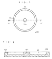
- FIG. 1 is a top view of a stage 100 of a semiconductor manufacturing apparatus according to a first preferred embodiment of the present invention.
- FIG. 2 shows the cross section taken along line A-A' of FIG. 1.
- the stage 100 has metal portions (first metal portion) 10a and 10b that are flat and made of metal, and an electroconductive elastic-body portion 20 that is flat and made of, e.g., electroconductive silicone rubber.
- the metal portions 10a and 10b and the electroconductive elastic-body portion 20 come in close contact with a single semiconductor substrate placed on the stage 100.
- the stage 100 is of vacuum suction type, a large number of holes for suction are formed in the metal portions 10a and 10b, which are not shown in FIGS. 1 and 2.
- the holes may be formed also in the electroconductive elastic-body portion 20.
- FIG. 3 is a cross-sectional view showing the stage 100 of FIG. 2 immediately before a semiconductor substrate (semiconductor wafer) 30 having a contaminant 40 adhering on the back, such as dust or Si particle, is placed on the stage 100.
- FIG. 4 is a cross-sectional view showing the stage 100 on which the semiconductor substrate 30 of FIG. 3 is set by suction. As shown in FIG. 4, the contaminant 40 is embedded in the electroconductive elastic-body portion 20 of the stage 100.
- the semiconductor substrate 30 is set on the stage 100 by suction, the stress applied to the semiconductor substrate 30 due to the contaminant 40 is reduced and the semiconductor substrate 30 is kept flat, whereby the semiconductor substrate 30 is prevented from breaking and deforming.
- the ratio between the surface area of the metal portions 10a and 10b and the surface area of the electroconductive elastic-body portion 20 can be arbitrarily determined, but the rate of breakage of the semiconductor substrate 30 can be reduced by increasing the percentage of the surface area of the electroconductive elastic-body portion 20 in the surface area of the stage 100.
- the rate of breakage of the semiconductor substrate 30 is greatly reduced when the surface area of the electroconductive elastic-body portion 20 makes up 50% or more of the surface area of the stage 100.
- the circular metal portion 10a is formed in the center of the stage 100, the ring-shaped metal portion 10b is formed along the circumference of the stage 100, and the electroconductive elastic-body portion 20 is formed between the metal portion 10a and the metal portion 10b.
- This arrangement allows the electroconductive elastic-body portion 20 to occupy an increased percentage of the surface area of the stage 100, so as to reduce the rate of breakage of the semiconductor substrate 30, while ensuring conductivity between the stage 100 and the semiconductor substrate 30.
- the surface area of the metal portion 10 may be increased as shown in FIGS. 5 to 7.
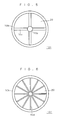
- FIG. 5 shows a stage 101 in which, in the stage 100 of FIG. 1, metal portions 10c are formed to radially extend in four directions from the center.
- FIG. 6 shows a stage 102 in which a metal portion 10d is formed to radially extend in 12 directions from the center, in place of the metal portion 10a of the stage 100 of FIG. 1.
- FIG. 7 shows a stage 103 in which a ring-shaped metal portion 10e is formed between the metal portion 10a and the metal portion 10b of the stage 100 shown in FIG. 1.
- the surface areas of the metal portions 10 occupy higher percentages than in the stage 100 shown in FIG. 1. This offers still higher conductivity than that of the stage 100, and is therefore suitable when the semiconductor substrate 30 is warped and the stage 100 is unable to ensure conductivity, for example.
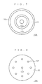
- FIG. 8 shows a stage 104 in which the central metal portion 10a of the stage 100 of FIG. 1 is replaced by a circular metal portion 10f smaller than the metal portion 10a, and the metal portion 10b is replaced by eight metal portions 10f arranged in the form of a ring.
- FIG. 9 shows a stage 105 in which nine metal portions 10f are arranged in the form of a cross.
- the surface area of the electroconductive elastic-body portion 20 makes up higher percentages than in the stage 100 shown in FIG. 1. The rate of breakage is thus further reduced as compared with the stage 100.
- the forms of the metal portion 10 and the electroconductive elastic-body portion 20 can be arbitrarily determined to adjust the conductivity and the rate of breakage of the semiconductor substrate 30.
- the material of the electroconductive elastic-body portion 20 is not limited to electroconductive silicone rubber, but the electroconductive elastic-body portion 20 may be made of any elastic body having conductivity.
- the flat, electroconductive elastic-body portion 20 of electroconductive silicone rubber is partially formed so that the contaminant 40 is embedded therein to reduce the stress applied to the semiconductor substrate 30.
- a metal portion made of surface-roughened metal may be formed in place of the electroconductive elastic-body portion 20.
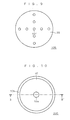
- FIG. 10 is a top view showing a stage 200 of a semiconductor manufacturing apparatus according to a second preferred embodiment of the present invention.
- FIG. 11 is an enlarged view showing a part of the cross section taken along line B-B' of FIG. 10.
- the electroconductive elastic-body portion 20 of FIG. 1 is replaced by a metal portion (a second metal portion) 50 that is made of surface-roughened metal.
- the surface of the metal portion 50 has uncounted numbers of recessed portions (recesses) 51 and raised portions 52.
- the metal portions 10a and 10b and the raised portions 52 come in close contact with a single semiconductor substrate 30 placed on the stage 200.
- the stage 200 is of vacuum suction type, a large number of holes for suction are formed in the metal portions 10a and 10b, which are not shown in FIGS. 10 and 11.
- FIG. 12 is a cross-sectional view showing the stage 200 of FIG. 11 immediately before a semiconductor substrate 30, having a contaminant 40 on its back, is placed on the stage 200.
- FIG. 13 is a cross-sectional view showing the stage 200 on which the semiconductor substrate 30 of FIG. 12 is set by suction.
- the contaminant 40 adheres to the back of the semiconductor substrate 30 above a recessed portion 51, the contaminant 40 comes in the recessed portion 51 of the stage 200 as shown in FIG. 13.
- the semiconductor substrate 30 when the semiconductor substrate 30 is set on the stage 200 by suction, the stress applied to the semiconductor substrate 30 due to the contaminant 40 is reduced, and the semiconductor substrate 30 is kept flat, whereby breakage and deformation of the semiconductor substrate 30 are prevented.
- the ratio between the surface area of the metal portions 10a and 10b and the surface area of the metal portion 50 can be arbitrarily determined, but, as in the first preferred embodiment, the rate of breakage of the semiconductor substrate 30 can be reduced by increasing the percentage of the surface area of the metal portion 50 in the surface area of the stage 100. In particular, it has been found that the rate of breakage of the semiconductor substrate 30 is greatly reduced when the surface area of the metal portion 50 makes up 50% or more of the surface area of the stage 100.
- the circular metal portion 10a is formed in the center of the stage 200, the ring-shaped metal portion 10b is formed along the circumference of the stage 200, and the metal portion 50 is formed between the metal portion 10a and the metal portion 10b.
- this arrangement allows the metal portion 50 to occupy an increased percentage of the surface area of the stage 200, so as to reduce the rate of breakage of the semiconductor substrate 30, while ensuring conductivity between the stage 200 and the semiconductor substrate 30.
- the surface area of the metal portion 10 may be increased as shown in FIGS. 14 to 16.
- FIGS. 14 to 16 show examples in which, in the structures of FIGS. 5 to 7, the metal portion 50 is formed in place of the electroconductive elastic-body portion 20.
- the surface areas of the metal portions 10 make up higher percentages than in the stage 200 shown in FIG. 10. This offers still higher conductivity than that of the stage 200, and is therefore suitable when the semiconductor substrate 30 is warped and the stage 200 is unable to ensure conductivity, for example.
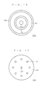
- FIGS. 17 and 18 show examples in which, in the structures of FIGS. 8 and 9, the metal portion 50 is formed in place of the electroconductive elastic-body portion 20.
- the surface areas of the metal portions 50 make up higher percentages than in the stage 200 shown in FIG. 10. The rate of breakage is thus further reduced than with the stage 200.
- the forms of the metal portion 10 and the metal portion 50 can be arbitrarily determined to adjust the conductivity and the rate of breakage of the semiconductor substrate 30.
- FIGS. 11 to 13 have shown an example in which the recessed portions 51 in the metal portion 50 are rectangularly shaped in cross section, but recessed portions 53 that are curved in cross section as shown in FIG. 19 may be formed in place of the rectangular recessed portions 51.
- both of recessed portions 51 and 53 may be formed. That is, the depths, areas, shapes, and positions of the holes and recessed portions 51 and 53 may be determined arbitrarily. It is known that the rate of breakage of the semiconductor substrate 30 is greatly reduced when the recessed portions 51 and 53 have an area of 1 to 10000 ⁇ m 2 and a depth of 1 to 100 ⁇ m.
- the recessed portions 51 and 53 of FIGS. 11, 19 and 20 may be filled with an electroconductive elastic body 60. That is, FIGS. 21 to 23 respectively show examples in which the recessed portions 51 and 53 of FIGS. 11, 19 and 20 are filled with electroconductive elastic body 60. Filling the recessed portions 51 and 53 with the electroconductive elastic body 60 alleviates abnormal discharge when high voltage is applied between the first and second main surfaces of the semiconductor substrate 30 or between the stage 200 and an upper electrode formed on the first main surface of the semiconductor substrate 30.
- the electroconductive elastic-body portions 20 of the stages 100 to 105 of the first preferred embodiment are replaced by the metal portion 50 made of surface-roughened metal. As in the first preferred embodiment, this prevents breakage and deformation of the semiconductor substrate 30 without deteriorating operability in processing or inspections.
- the metal portion 50 is made of surface-roughened metal
- the metal portion 50 may be processed in other ways than surface roughening, as long as the metal portion 50 has countless numbers of recesses formed in its surface.
Landscapes
- Container, Conveyance, Adherence, Positioning, Of Wafer (AREA)
- Die Bonding (AREA)
Abstract
Description
- The present invention relates to semiconductor manufacturing apparatuses, and particularly to processing of semiconductor substrates.
- With vertical semiconductor devices in which current flows between the first and second main surfaces of the semiconductor substrate (semiconductor wafer), the semiconductor substrates are being made thinner and thinner in order to achieve improvements in characteristics (e.g., to reduce on-state voltage). In a common single-wafer-processing semiconductor manufacturing apparatus, the semiconductor substrates are transported to a metal stage having an approximately flat surface and are set on the stage by suction.
- Now, thin semiconductor substrates, having a diameter of 6 inches and a thickness of 200 µm or less, for example, have reduced strength. Also, when contaminants such as dust and dust particles of Si attach to the back of a semiconductor substrate and the semiconductor substrate is placed on the stage for processing or for inspection, the contaminants are sandwiched between the semiconductor substrate and the stage. If the contaminants have certain or higher hardness, the semiconductor substrate undergoes considerable stress at and around the contaminants, which may result in breakage or deformation of the semiconductor substrate.
- To solve this problem, Patent Document 1 discloses an example of a semiconductor manufacturing apparatus in which a buffer made of an elastic body is interposed between the semiconductor substrate and stage. Also, Patent Documents 2 to 4 disclose examples of semiconductor manufacturing apparatuses in which holes, or the like, are formed in the surface of the stage.
-
- Patent Document 1:
Japanese Patent Application Laid-Open No. 55-43853 (1980 - Patent Document 2:
Japanese Patent Application Laid-Open No. 62-199030 (1987 - Patent Document 3:
Japanese Patent Application Laid-Open No. 59-135742 (1984 - Patent Document 4:
Japanese Patent Application Laid-Open No. 4-152512 (1992 - In the semiconductor manufacturing apparatus disclosed in Patent Document 1, the presence of the buffer, separate from the stage, is likely to deteriorate operability in processing. Also, in the semiconductor manufacturing apparatuses disclosed in Patent Documents 2 to 4, semiconductor substrates are sucked from the holes, or the like, formed in the surface of the stage. Accordingly, when the holes, or the like, are large, the semiconductor substrates undergo considerable stress at and around the holes, which may also result in breakage or deformation of the semiconductor substrates.
- The present invention has been made to solve the problems above, and an object of the invention is to provide a semiconductor manufacturing apparatus capable of preventing breakage and deformation of semiconductor substrates without deteriorating operability in processing.
- A first aspect of the present invention provides a semiconductor manufacturing apparatus having a stage (100 to 105) on which a semiconductor substrate (30) is placed, and the stage (100 to 105) comprises a first metal portion (10) that is made of metal and that comes in contact with the semiconductor substrate (30) placed thereon and an electroconductive elastic-body portion (20) that is made of an electroconductive elastic body and that comes in contact with the semiconductor substrate (30) placed thereon.
- According to the semiconductor manufacturing apparatus of the first aspect of the invention, when the semiconductor substrate (30) is placed on the stage (100 to 105), the stress applied to the semiconductor substrate (30) when a contaminant adheres on its back is reduced, and the semiconductor substrate (30) is kept flat. This prevents breakage and deformation of the semiconductor substrate (30) without deteriorating operability in processing.
- A second aspect of the present invention provides a semiconductor manufacturing apparatus having a stage (200 to 205) on which a semiconductor substrate (30) is placed, and the stage (200 to 205) comprises a first metal portion (10) that is made of metal not processed to form countless numbers of recesses (51, 53) in its surface and that comes in contact with the semiconductor substrate (30) placed thereon, and a second metal portion (50) that is made of metal processed to form countless numbers of recesses (51, 53) in its surface and that comes in contact with the semiconductor substrate (30) placed thereon.
- According to the semiconductor manufacturing apparatus of the second aspect of the invention, when the semiconductor substrate (30) is placed on the stage (200 to 205), the stress applied to the semiconductor substrate (30) when a contaminant adheres on its back is reduced, and the semiconductor substrate (30) is kept flat. This prevents breakage and deformation of the semiconductor substrate (30) without deteriorating operability in processing.
- These and other objects, features, aspects and advantages of the present invention will become more apparent from the following detailed description of the present invention when taken in conjunction with the accompanying drawings.
-
- FIG. 1 is a top view of a stage according to a first preferred embodiment of the invention.
- FIG. 2 is a cross-sectional view of the stage.
- FIG. 3 is a cross-sectional view of the stage.
- FIG. 4 is a cross-sectional view of the stage.
- FIG. 5 is a top view of a stage.
- FIG. 6 is a top view of a stage.
- FIG. 7 is a top view of a stage.
- FIG. 8 is a top view of a stage.
- FIG. 9 is a top view of a stage.
- FIG. 10 is a top view of a stage according to a second preferred embodiment of the invention.
- FIG. 11 is an enlarged cross-sectional view of a part of the stage.
- FIG. 12 is an enlarged cross-sectional view of the part of the stage.
- FIG. 13 is an enlarged cross-sectional view of the part of the stage.
- FIG. 14 is a top view of a stage.
- FIG. 15 is a top view of a stage.
- FIG. 16 is a top view of a stage.
- FIG. 17 is a top view of a stage.
- FIG. 18 is a top view of a stage.
- FIG. 19 is an enlarged cross-sectional view of a part of a stage.
- FIG. 20 is an enlarged cross-sectional view of a part of a stage.
- FIG. 21 is an enlarged cross-sectional view of a part of a stage.
- FIG. 22 is an enlarged cross-sectional view of a part of a stage.
- FIG. 23 is an enlarged cross-sectional view of a part of a stage.
- FIG. 1 is a top view of a
stage 100 of a semiconductor manufacturing apparatus according to a first preferred embodiment of the present invention. FIG. 2 shows the cross section taken along line A-A' of FIG. 1. - As shown in FIGS. 1 and 2, the
stage 100 has metal portions (first metal portion) 10a and 10b that are flat and made of metal, and an electroconductive elastic-body portion 20 that is flat and made of, e.g., electroconductive silicone rubber. Themetal portions body portion 20 come in close contact with a single semiconductor substrate placed on thestage 100. When thestage 100 is of vacuum suction type, a large number of holes for suction are formed in themetal portions body portion 20. - FIG. 3 is a cross-sectional view showing the
stage 100 of FIG. 2 immediately before a semiconductor substrate (semiconductor wafer) 30 having a contaminant 40 adhering on the back, such as dust or Si particle, is placed on thestage 100. FIG. 4 is a cross-sectional view showing thestage 100 on which thesemiconductor substrate 30 of FIG. 3 is set by suction. As shown in FIG. 4, the contaminant 40 is embedded in the electroconductive elastic-body portion 20 of thestage 100. Thus, when thesemiconductor substrate 30 is set on thestage 100 by suction, the stress applied to thesemiconductor substrate 30 due to the contaminant 40 is reduced and thesemiconductor substrate 30 is kept flat, whereby thesemiconductor substrate 30 is prevented from breaking and deforming. - In the
stage 100 of FIG. 1, the ratio between the surface area of themetal portions body portion 20 can be arbitrarily determined, but the rate of breakage of thesemiconductor substrate 30 can be reduced by increasing the percentage of the surface area of the electroconductive elastic-body portion 20 in the surface area of thestage 100. In particular, it has been found that the rate of breakage of thesemiconductor substrate 30 is greatly reduced when the surface area of the electroconductive elastic-body portion 20 makes up 50% or more of the surface area of thestage 100. - In the example of FIG. 1, the
circular metal portion 10a is formed in the center of thestage 100, the ring-shaped metal portion 10b is formed along the circumference of thestage 100, and the electroconductive elastic-body portion 20 is formed between themetal portion 10a and themetal portion 10b. This arrangement allows the electroconductive elastic-body portion 20 to occupy an increased percentage of the surface area of thestage 100, so as to reduce the rate of breakage of thesemiconductor substrate 30, while ensuring conductivity between thestage 100 and thesemiconductor substrate 30. - When the process requires higher conductivity, or when the
semiconductor substrate 30 is warped and conductivity cannot be ensured with thestage 100, for example, the surface area of themetal portion 10 may be increased as shown in FIGS. 5 to 7. - FIG. 5 shows a
stage 101 in which, in thestage 100 of FIG. 1,metal portions 10c are formed to radially extend in four directions from the center. - FIG. 6 shows a
stage 102 in which ametal portion 10d is formed to radially extend in 12 directions from the center, in place of themetal portion 10a of thestage 100 of FIG. 1. - FIG. 7 shows a
stage 103 in which a ring-shapedmetal portion 10e is formed between themetal portion 10a and themetal portion 10b of thestage 100 shown in FIG. 1. - In the
stages 101 to 103 shown in FIGS. 5 to 7, the surface areas of themetal portions 10 occupy higher percentages than in thestage 100 shown in FIG. 1. This offers still higher conductivity than that of thestage 100, and is therefore suitable when thesemiconductor substrate 30 is warped and thestage 100 is unable to ensure conductivity, for example. - FIG. 8 shows a
stage 104 in which thecentral metal portion 10a of thestage 100 of FIG. 1 is replaced by acircular metal portion 10f smaller than themetal portion 10a, and themetal portion 10b is replaced by eightmetal portions 10f arranged in the form of a ring. - FIG. 9 shows a
stage 105 in which ninemetal portions 10f are arranged in the form of a cross. - In the
stages body portion 20 makes up higher percentages than in thestage 100 shown in FIG. 1. The rate of breakage is thus further reduced as compared with thestage 100. - That is, the forms of the
metal portion 10 and the electroconductive elastic-body portion 20 can be arbitrarily determined to adjust the conductivity and the rate of breakage of thesemiconductor substrate 30. - In this way, in the
stages 100 to 105 of this preferred embodiment, when thesemiconductor substrate 30 is set by vacuum or electrostatic chuck equipment, for example, the presence of the electroconductive elastic-body portion 20, which is flat and made of, e.g., electroconductive silicone rubber, reduces the stress applied to thesemiconductor substrate 30 due to thecontaminant 40 adhering on the back of thesemiconductor substrate 30, and thesemiconductor substrate 30 is kept flat. This prevents breakage and deformation of thesemiconductor substrate 30 without deteriorating operability in processing or inspections. - While the description above has shown examples in which the electroconductive elastic-
body portion 20 is made of electroconductive silicone rubber, the material of the electroconductive elastic-body portion 20 is not limited to electroconductive silicone rubber, but the electroconductive elastic-body portion 20 may be made of any elastic body having conductivity. - In the
stages 100 to 105 of the first preferred embodiment, the flat, electroconductive elastic-body portion 20 of electroconductive silicone rubber is partially formed so that thecontaminant 40 is embedded therein to reduce the stress applied to thesemiconductor substrate 30. However, a metal portion made of surface-roughened metal may be formed in place of the electroconductive elastic-body portion 20. - FIG. 10 is a top view showing a
stage 200 of a semiconductor manufacturing apparatus according to a second preferred embodiment of the present invention. FIG. 11 is an enlarged view showing a part of the cross section taken along line B-B' of FIG. 10. - In FIG. 10, the electroconductive elastic-
body portion 20 of FIG. 1 is replaced by a metal portion (a second metal portion) 50 that is made of surface-roughened metal. As shown in FIG. 11, the surface of themetal portion 50 has uncounted numbers of recessed portions (recesses) 51 and raisedportions 52. Themetal portions portions 52 come in close contact with asingle semiconductor substrate 30 placed on thestage 200. When thestage 200 is of vacuum suction type, a large number of holes for suction are formed in themetal portions portions 51 but only in themetal portions semiconductor substrate 30 at holes formed in the recessedportions 51, thus preventing breakage or deformation of thesemiconductor substrate 30. - FIG. 12 is a cross-sectional view showing the
stage 200 of FIG. 11 immediately before asemiconductor substrate 30, having acontaminant 40 on its back, is placed on thestage 200. FIG. 13 is a cross-sectional view showing thestage 200 on which thesemiconductor substrate 30 of FIG. 12 is set by suction. In FIG. 12, when thecontaminant 40 adheres to the back of thesemiconductor substrate 30 above a recessedportion 51, thecontaminant 40 comes in the recessedportion 51 of thestage 200 as shown in FIG. 13. Thus, as in the first preferred embodiment, when thesemiconductor substrate 30 is set on thestage 200 by suction, the stress applied to thesemiconductor substrate 30 due to thecontaminant 40 is reduced, and thesemiconductor substrate 30 is kept flat, whereby breakage and deformation of thesemiconductor substrate 30 are prevented. - In FIG. 12, when the
contaminant 40 adheres to the back of thesemiconductor substrate 30 not above a recessedportion 51 but above a raisedportion 52, the flow of air caused by suction pushes thecontaminant 40 toward a recessedportion 51, and thecontaminant 40 comes in the recessedportion 51. - In the
stage 200 of FIG. 10, the ratio between the surface area of themetal portions metal portion 50 can be arbitrarily determined, but, as in the first preferred embodiment, the rate of breakage of thesemiconductor substrate 30 can be reduced by increasing the percentage of the surface area of themetal portion 50 in the surface area of thestage 100. In particular, it has been found that the rate of breakage of thesemiconductor substrate 30 is greatly reduced when the surface area of themetal portion 50 makes up 50% or more of the surface area of thestage 100. - In the example of FIG. 10, the
circular metal portion 10a is formed in the center of thestage 200, the ring-shapedmetal portion 10b is formed along the circumference of thestage 200, and themetal portion 50 is formed between themetal portion 10a and themetal portion 10b. As in the first preferred embodiment, this arrangement allows themetal portion 50 to occupy an increased percentage of the surface area of thestage 200, so as to reduce the rate of breakage of thesemiconductor substrate 30, while ensuring conductivity between thestage 200 and thesemiconductor substrate 30. - Also, as in the first preferred embodiment, when the process requires higher conductivity, or when the
semiconductor substrate 30 is warped and conductivity cannot be ensured with thestage 200, for example, the surface area of themetal portion 10 may be increased as shown in FIGS. 14 to 16. - FIGS. 14 to 16 show examples in which, in the structures of FIGS. 5 to 7, the
metal portion 50 is formed in place of the electroconductive elastic-body portion 20. - In the
stages 201 to 203 shown in FIGS. 14 to 16, the surface areas of themetal portions 10 make up higher percentages than in thestage 200 shown in FIG. 10. This offers still higher conductivity than that of thestage 200, and is therefore suitable when thesemiconductor substrate 30 is warped and thestage 200 is unable to ensure conductivity, for example. - FIGS. 17 and 18 show examples in which, in the structures of FIGS. 8 and 9, the
metal portion 50 is formed in place of the electroconductive elastic-body portion 20. - In the
stages metal portions 50 make up higher percentages than in thestage 200 shown in FIG. 10. The rate of breakage is thus further reduced than with thestage 200. - That is, the forms of the
metal portion 10 and themetal portion 50 can be arbitrarily determined to adjust the conductivity and the rate of breakage of thesemiconductor substrate 30. - FIGS. 11 to 13 have shown an example in which the recessed
portions 51 in themetal portion 50 are rectangularly shaped in cross section, but recessedportions 53 that are curved in cross section as shown in FIG. 19 may be formed in place of the rectangular recessedportions 51. Alternatively, as shown in FIG. 20, both of recessedportions portions semiconductor substrate 30 is greatly reduced when the recessedportions - Also, as shown in FIGS. 21 to 23, the recessed
portions elastic body 60. That is, FIGS. 21 to 23 respectively show examples in which the recessedportions elastic body 60. Filling the recessedportions elastic body 60 alleviates abnormal discharge when high voltage is applied between the first and second main surfaces of thesemiconductor substrate 30 or between thestage 200 and an upper electrode formed on the first main surface of thesemiconductor substrate 30. - In this way, in the
stages 200 to 205 of this preferred embodiment, the electroconductive elastic-body portions 20 of thestages 100 to 105 of the first preferred embodiment are replaced by themetal portion 50 made of surface-roughened metal. As in the first preferred embodiment, this prevents breakage and deformation of thesemiconductor substrate 30 without deteriorating operability in processing or inspections. - While the description above has shown examples in which the
metal portion 50 is made of surface-roughened metal, themetal portion 50 may be processed in other ways than surface roughening, as long as themetal portion 50 has countless numbers of recesses formed in its surface. - While the invention has been described in detail, the foregoing description is in all aspects illustrative and not restrictive. It is understood that numerous other modifications and variations can be devised without departing from the scope of the invention.
Claims (9)
- A semiconductor manufacturing apparatus having a stage (100 to 105) on which a semiconductor substrate (30) is placed,
wherein said stage (100 to 105) comprises
a first metal portion (10) that is made of metal and that comes in contact with said semiconductor substrate (30) placed thereon; and
an electroconductive elastic-body portion (20) that is made of an electroconductive elastic body and that comes in contact with said semiconductor substrate (30) placed thereon. - The semiconductor manufacturing apparatus according to claim 1,
wherein said first metal portion (10) comprises a circular metal portion (10a) formed in a center of said stage (100, 103) and a ring-shaped metal portion (10b) formed along a periphery of said stage (100, 103). - The semiconductor manufacturing apparatus according to claim 1 or 2,
wherein said electroconductive elastic-body portion (20) has a surface area that makes up 50% or more of a surface area of said stage (100 to 105). - A semiconductor manufacturing apparatus having a stage (200 to 205) on which a semiconductor substrate (30) is placed,
wherein said stage (200 to 205) comprises
a first metal portion (10) that is made of metal not processed to form countless numbers of recesses (51, 53) in its surface and that comes in contact with said semiconductor substrate (30) placed thereon, and
a second metal portion (50) that is made of metal processed to form countless numbers of recesses (51, 53) in its surface and that comes in contact with said semiconductor substrate (30) placed thereon. - The semiconductor manufacturing apparatus according to claim 4,
wherein said first metal portion (10) has a plurality of holes formed for suction, and
said holes are absent in said recesses (51, 53). - The semiconductor manufacturing apparatus according to claim 4 or 5,
wherein said first metal portion (10) comprises a circular metal portion (10a) formed in a center of said stage (200, 203) and a ring-shaped metal portion (10b) formed along a periphery of said stage (200, 203). - The semiconductor manufacturing apparatus according to any of claims 4 to 6,
wherein said second metal portion (50) has a surface area that makes up 50% or more of a surface area of said stage (200 to 205). - The semiconductor manufacturing apparatus according to any of claims 4 to 7,
wherein said recesses (51, 53) have an area of 1 to 10000 µm2 and a depth of 1 to 100 µm. - The semiconductor manufacturing apparatus according to any of claims 4 to 8,
wherein said stage (200 to 205) further comprises an electroconductive elastic body (60) filling said recesses (51, 53).
Applications Claiming Priority (1)
| Application Number | Priority Date | Filing Date | Title |
|---|---|---|---|
| PCT/JP2005/000174 WO2006075356A1 (en) | 2005-01-11 | 2005-01-11 | Semiconductor manufacturing apparatus |
Publications (3)
| Publication Number | Publication Date |
|---|---|
| EP1796158A1 true EP1796158A1 (en) | 2007-06-13 |
| EP1796158A4 EP1796158A4 (en) | 2010-08-04 |
| EP1796158B1 EP1796158B1 (en) | 2016-05-18 |
Family
ID=36677392
Family Applications (1)
| Application Number | Title | Priority Date | Filing Date |
|---|---|---|---|
| EP05703413.4A Expired - Lifetime EP1796158B1 (en) | 2005-01-11 | 2005-01-11 | Semiconductor manufacturing apparatus |
Country Status (6)
| Country | Link |
|---|---|
| US (1) | US8696816B2 (en) |
| EP (1) | EP1796158B1 (en) |
| JP (1) | JP4611292B2 (en) |
| CN (1) | CN100511632C (en) |
| TW (1) | TWI280608B (en) |
| WO (1) | WO2006075356A1 (en) |
Families Citing this family (3)
| Publication number | Priority date | Publication date | Assignee | Title |
|---|---|---|---|---|
| JP5324231B2 (en) * | 2009-01-08 | 2013-10-23 | 日東電工株式会社 | Semiconductor wafer alignment system |
| CN103506927B (en) * | 2013-10-28 | 2015-12-02 | 中国科学院地球化学研究所 | A kind of polishing machine material containing block |
| CA2980304C (en) * | 2015-03-23 | 2021-07-06 | Hubbell Incorporated | Connectors for flexible busbar and methods of connecting |
Family Cites Families (15)
| Publication number | Priority date | Publication date | Assignee | Title |
|---|---|---|---|---|
| JPS5543853A (en) * | 1978-09-25 | 1980-03-27 | Hitachi Ltd | Dicing |
| JPS5913752B2 (en) | 1978-09-25 | 1984-03-31 | ヤマハ株式会社 | electronic musical instruments |
| JPS59135742A (en) | 1983-01-25 | 1984-08-04 | Toshiba Corp | Supporting device for semiconductor wafer |
| JPS62199030A (en) * | 1986-02-27 | 1987-09-02 | Nec Kyushu Ltd | Treatment device of semiconductor wafer |
| JP2574818B2 (en) | 1987-11-16 | 1997-01-22 | 株式会社日立製作所 | Vacuum suction fixing table and vacuum suction fixing method |
| JPH04152512A (en) | 1990-10-16 | 1992-05-26 | Fujitsu Ltd | Wafer chuck |
| JPH10107131A (en) * | 1996-09-25 | 1998-04-24 | Teikoku Seiki Kk | Suction table and element thereof |
| JPH10112495A (en) * | 1996-10-07 | 1998-04-28 | Dainippon Screen Mfg Co Ltd | Substrate holder |
| JP3469999B2 (en) | 1996-10-30 | 2003-11-25 | 京セラ株式会社 | Adsorber manufacturing method |
| JP4152512B2 (en) | 1999-01-11 | 2008-09-17 | 大成建設株式会社 | Sensible heat flow analysis method |
| JP2001209981A (en) * | 1999-02-09 | 2001-08-03 | Ricoh Co Ltd | Optical disk substrate film forming apparatus, optical disk substrate film forming method, substrate holder manufacturing method, substrate holder, optical disk, and phase change recording optical disk |
| DE19962170A1 (en) * | 1999-12-22 | 2001-07-12 | Steag Micro Tech Gmbh | Sub-beam holder |
| JP3390409B2 (en) * | 2000-06-02 | 2003-03-24 | エヌイーシーセミコンダクターズ九州株式会社 | Support frame attaching device |
| DE10308095B3 (en) * | 2003-02-24 | 2004-10-14 | Infineon Technologies Ag | Electronic component with at least one semiconductor chip on a circuit carrier and method for producing the same |
| JP2004265962A (en) * | 2003-02-28 | 2004-09-24 | Hirata Corp | Substrate rotating device |
-
2005
- 2005-01-11 US US11/571,971 patent/US8696816B2/en active Active
- 2005-01-11 JP JP2006519024A patent/JP4611292B2/en not_active Expired - Lifetime
- 2005-01-11 CN CNB2005800270071A patent/CN100511632C/en not_active Expired - Lifetime
- 2005-01-11 EP EP05703413.4A patent/EP1796158B1/en not_active Expired - Lifetime
- 2005-01-11 WO PCT/JP2005/000174 patent/WO2006075356A1/en not_active Ceased
- 2005-03-16 TW TW094108005A patent/TWI280608B/en not_active IP Right Cessation
Also Published As
| Publication number | Publication date |
|---|---|
| US20070228628A1 (en) | 2007-10-04 |
| JP4611292B2 (en) | 2011-01-12 |
| TW200625399A (en) | 2006-07-16 |
| CN101019221A (en) | 2007-08-15 |
| JPWO2006075356A1 (en) | 2008-06-12 |
| WO2006075356A1 (en) | 2006-07-20 |
| TWI280608B (en) | 2007-05-01 |
| US8696816B2 (en) | 2014-04-15 |
| CN100511632C (en) | 2009-07-08 |
| EP1796158A4 (en) | 2010-08-04 |
| EP1796158B1 (en) | 2016-05-18 |
Similar Documents
| Publication | Publication Date | Title |
|---|---|---|
| US10431489B2 (en) | Substrate support apparatus having reduced substrate particle generation | |
| US8517803B2 (en) | Retaining ring for chemical mechanical polishing | |
| TWI660247B (en) | Substrate holding member | |
| CN110277341A (en) | Electrostatic chuck | |
| EP2202786A1 (en) | Plasma film forming apparatus | |
| CN213366557U (en) | Multilayer electrostatic chuck assembly | |
| MY167045A (en) | Sealed elastomer bonded si electrodes and the like for reduced particle contamination in dielectric etch | |
| CN111668150A (en) | Electrostatic chuck and processing device | |
| CN111668148A (en) | Electrostatic chuck and processing device | |
| CN106796909A (en) | Electrostatic chuck with radio frequency branch | |
| CN105575874A (en) | Clamp assembly | |
| US8696816B2 (en) | Semiconductor manufacturing apparatus | |
| JP2019169629A (en) | Board retainer | |
| JP5146056B2 (en) | Semiconductor device manufacturing method and semiconductor device support device | |
| KR20120007017A (en) | Receiving device for accommodating semiconductor substrate | |
| US20100144147A1 (en) | Sample holding tool, sample suction device using the same and sample processing method using the same | |
| JP2009055017A (en) | Holding jig and suction device using the same | |
| US20140057052A1 (en) | Wafer support device | |
| KR100841381B1 (en) | Semiconductor manufacturing device | |
| CN116313991A (en) | Wafer overturning device | |
| JP2004221266A (en) | Ring component for semiconductor equipment | |
| KR100717694B1 (en) | Electrostatic chuck with separating layer | |
| JP2002368068A (en) | Suction stage | |
| JP4590314B2 (en) | Wafer carrier | |
| JP2005085979A (en) | Electrostatic chuck |
Legal Events
| Date | Code | Title | Description |
|---|---|---|---|
| PUAI | Public reference made under article 153(3) epc to a published international application that has entered the european phase |
Free format text: ORIGINAL CODE: 0009012 |
|
| 17P | Request for examination filed |
Effective date: 20070112 |
|
| AK | Designated contracting states |
Kind code of ref document: A1 Designated state(s): DE FR NL |
|
| DAX | Request for extension of the european patent (deleted) | ||
| RBV | Designated contracting states (corrected) |
Designated state(s): DE FR NL |
|
| A4 | Supplementary search report drawn up and despatched |
Effective date: 20100705 |
|
| RIC1 | Information provided on ipc code assigned before grant |
Ipc: B65C 11/04 20060101ALI20100629BHEP Ipc: H01L 21/68 20060101AFI20060726BHEP |
|
| 17Q | First examination report despatched |
Effective date: 20130426 |
|
| REG | Reference to a national code |
Ref country code: DE Ref legal event code: R079 Ref document number: 602005049363 Country of ref document: DE Free format text: PREVIOUS MAIN CLASS: H01L0021680000 Ipc: H01L0021670000 |
|
| GRAP | Despatch of communication of intention to grant a patent |
Free format text: ORIGINAL CODE: EPIDOSNIGR1 |
|
| INTG | Intention to grant announced |
Effective date: 20151202 |
|
| RIC1 | Information provided on ipc code assigned before grant |
Ipc: H01L 21/687 20060101ALI20151123BHEP Ipc: H01L 21/677 20060101ALI20151123BHEP Ipc: H01L 21/67 20060101AFI20151123BHEP |
|
| GRAS | Grant fee paid |
Free format text: ORIGINAL CODE: EPIDOSNIGR3 |
|
| GRAA | (expected) grant |
Free format text: ORIGINAL CODE: 0009210 |
|
| AK | Designated contracting states |
Kind code of ref document: B1 Designated state(s): DE FR NL |
|
| REG | Reference to a national code |
Ref country code: DE Ref legal event code: R096 Ref document number: 602005049363 Country of ref document: DE |
|
| REG | Reference to a national code |
Ref country code: NL Ref legal event code: MP Effective date: 20160518 |
|
| PG25 | Lapsed in a contracting state [announced via postgrant information from national office to epo] |
Ref country code: NL Free format text: LAPSE BECAUSE OF FAILURE TO SUBMIT A TRANSLATION OF THE DESCRIPTION OR TO PAY THE FEE WITHIN THE PRESCRIBED TIME-LIMIT Effective date: 20160518 |
|
| REG | Reference to a national code |
Ref country code: DE Ref legal event code: R097 Ref document number: 602005049363 Country of ref document: DE |
|
| PLBE | No opposition filed within time limit |
Free format text: ORIGINAL CODE: 0009261 |
|
| STAA | Information on the status of an ep patent application or granted ep patent |
Free format text: STATUS: NO OPPOSITION FILED WITHIN TIME LIMIT |
|
| 26N | No opposition filed |
Effective date: 20170221 |
|
| REG | Reference to a national code |
Ref country code: FR Ref legal event code: ST Effective date: 20170929 |
|
| PG25 | Lapsed in a contracting state [announced via postgrant information from national office to epo] |
Ref country code: FR Free format text: LAPSE BECAUSE OF NON-PAYMENT OF DUE FEES Effective date: 20170131 |
|
| REG | Reference to a national code |
Ref country code: DE Ref legal event code: R084 Ref document number: 602005049363 Country of ref document: DE |
|
| P01 | Opt-out of the competence of the unified patent court (upc) registered |
Effective date: 20230512 |
|
| PGFP | Annual fee paid to national office [announced via postgrant information from national office to epo] |
Ref country code: DE Payment date: 20231128 Year of fee payment: 20 |
|
| REG | Reference to a national code |
Ref country code: DE Ref legal event code: R071 Ref document number: 602005049363 Country of ref document: DE |