EP1796107A1 - Transparent conductor, transparent electrode, solar cell, luminescent device and display panel - Google Patents
Transparent conductor, transparent electrode, solar cell, luminescent device and display panel Download PDFInfo
- Publication number
- EP1796107A1 EP1796107A1 EP05770464A EP05770464A EP1796107A1 EP 1796107 A1 EP1796107 A1 EP 1796107A1 EP 05770464 A EP05770464 A EP 05770464A EP 05770464 A EP05770464 A EP 05770464A EP 1796107 A1 EP1796107 A1 EP 1796107A1
- Authority
- EP
- European Patent Office
- Prior art keywords
- metal oxide
- transparent conductor
- conductor according
- transparent
- tio
- Prior art date
- Legal status (The legal status is an assumption and is not a legal conclusion. Google has not performed a legal analysis and makes no representation as to the accuracy of the status listed.)
- Withdrawn
Links
- 239000004020 conductor Substances 0.000 title claims description 74
- 229910044991 metal oxide Inorganic materials 0.000 claims abstract description 124
- 150000004706 metal oxides Chemical class 0.000 claims abstract description 124
- GWEVSGVZZGPLCZ-UHFFFAOYSA-N Titan oxide Chemical compound O=[Ti]=O GWEVSGVZZGPLCZ-UHFFFAOYSA-N 0.000 claims abstract description 118
- 239000000758 substrate Substances 0.000 claims abstract description 46
- 239000013078 crystal Substances 0.000 claims abstract description 26
- 229910052715 tantalum Inorganic materials 0.000 claims abstract description 13
- 229910052758 niobium Inorganic materials 0.000 claims abstract description 11
- 229910052787 antimony Inorganic materials 0.000 claims abstract description 7
- 229910052785 arsenic Inorganic materials 0.000 claims abstract description 7
- 229910052750 molybdenum Inorganic materials 0.000 claims abstract description 7
- XLOMVQKBTHCTTD-UHFFFAOYSA-N zinc oxide Inorganic materials [Zn]=O XLOMVQKBTHCTTD-UHFFFAOYSA-N 0.000 claims description 23
- MCMNRKCIXSYSNV-UHFFFAOYSA-N Zirconium dioxide Chemical compound O=[Zr]=O MCMNRKCIXSYSNV-UHFFFAOYSA-N 0.000 claims description 12
- JMASRVWKEDWRBT-UHFFFAOYSA-N Gallium nitride Chemical compound [Ga]#N JMASRVWKEDWRBT-UHFFFAOYSA-N 0.000 claims description 7
- 229910052721 tungsten Inorganic materials 0.000 claims description 5
- 229910052748 manganese Inorganic materials 0.000 claims description 4
- 229910052720 vanadium Inorganic materials 0.000 claims description 4
- 229910002244 LaAlO3 Inorganic materials 0.000 claims description 3
- PNEYBMLMFCGWSK-UHFFFAOYSA-N aluminium oxide Inorganic materials [O-2].[O-2].[O-2].[Al+3].[Al+3] PNEYBMLMFCGWSK-UHFFFAOYSA-N 0.000 claims description 3
- 229910052797 bismuth Inorganic materials 0.000 claims description 3
- CETPSERCERDGAM-UHFFFAOYSA-N ceric oxide Chemical compound O=[Ce]=O CETPSERCERDGAM-UHFFFAOYSA-N 0.000 claims description 3
- 229910000422 cerium(IV) oxide Inorganic materials 0.000 claims description 3
- 229910052593 corundum Inorganic materials 0.000 claims description 3
- CPLXHLVBOLITMK-UHFFFAOYSA-N magnesium oxide Inorganic materials [Mg]=O CPLXHLVBOLITMK-UHFFFAOYSA-N 0.000 claims description 3
- 229910052698 phosphorus Inorganic materials 0.000 claims description 3
- 229910052702 rhenium Inorganic materials 0.000 claims description 3
- 229910052713 technetium Inorganic materials 0.000 claims description 3
- 229910001845 yogo sapphire Inorganic materials 0.000 claims description 3
- 229910002370 SrTiO3 Inorganic materials 0.000 claims 1
- 238000002834 transmittance Methods 0.000 abstract description 37
- 239000010409 thin film Substances 0.000 abstract description 15
- 239000000126 substance Substances 0.000 abstract description 9
- 239000002994 raw material Substances 0.000 abstract description 6
- 238000012423 maintenance Methods 0.000 abstract 1
- 239000007769 metal material Substances 0.000 abstract 1
- 239000010408 film Substances 0.000 description 51
- 238000010586 diagram Methods 0.000 description 30
- 229910052751 metal Inorganic materials 0.000 description 30
- 239000002184 metal Substances 0.000 description 30
- 230000003287 optical effect Effects 0.000 description 27
- 238000000034 method Methods 0.000 description 25
- 238000002441 X-ray diffraction Methods 0.000 description 19
- 239000000463 material Substances 0.000 description 17
- 239000004973 liquid crystal related substance Substances 0.000 description 13
- 238000005259 measurement Methods 0.000 description 13
- 238000004549 pulsed laser deposition Methods 0.000 description 12
- 239000011787 zinc oxide Substances 0.000 description 11
- 125000004429 atom Chemical group 0.000 description 10
- 230000037230 mobility Effects 0.000 description 10
- 238000005401 electroluminescence Methods 0.000 description 9
- 238000006467 substitution reaction Methods 0.000 description 9
- 229910052719 titanium Inorganic materials 0.000 description 9
- 230000007423 decrease Effects 0.000 description 7
- 238000004519 manufacturing process Methods 0.000 description 7
- 238000005240 physical vapour deposition Methods 0.000 description 6
- 230000008569 process Effects 0.000 description 6
- 230000009467 reduction Effects 0.000 description 6
- MYMOFIZGZYHOMD-UHFFFAOYSA-N Dioxygen Chemical compound O=O MYMOFIZGZYHOMD-UHFFFAOYSA-N 0.000 description 5
- 229910001882 dioxygen Inorganic materials 0.000 description 5
- 239000011521 glass Substances 0.000 description 5
- 238000005229 chemical vapour deposition Methods 0.000 description 4
- 238000004891 communication Methods 0.000 description 4
- 238000000151 deposition Methods 0.000 description 4
- 239000002019 doping agent Substances 0.000 description 4
- 239000000203 mixture Substances 0.000 description 4
- 229910052760 oxygen Inorganic materials 0.000 description 4
- 238000005498 polishing Methods 0.000 description 4
- 238000001228 spectrum Methods 0.000 description 4
- XOLBLPGZBRYERU-UHFFFAOYSA-N tin dioxide Chemical compound O=[Sn]=O XOLBLPGZBRYERU-UHFFFAOYSA-N 0.000 description 4
- QVGXLLKOCUKJST-UHFFFAOYSA-N atomic oxygen Chemical compound [O] QVGXLLKOCUKJST-UHFFFAOYSA-N 0.000 description 3
- 230000008901 benefit Effects 0.000 description 3
- 230000000903 blocking effect Effects 0.000 description 3
- 239000000969 carrier Substances 0.000 description 3
- 238000000576 coating method Methods 0.000 description 3
- 230000003247 decreasing effect Effects 0.000 description 3
- 239000010432 diamond Substances 0.000 description 3
- 229910003460 diamond Inorganic materials 0.000 description 3
- 239000012535 impurity Substances 0.000 description 3
- 238000001451 molecular beam epitaxy Methods 0.000 description 3
- 239000001301 oxygen Substances 0.000 description 3
- 239000002245 particle Substances 0.000 description 3
- 239000011941 photocatalyst Substances 0.000 description 3
- 230000001105 regulatory effect Effects 0.000 description 3
- 239000004065 semiconductor Substances 0.000 description 3
- 239000002002 slurry Substances 0.000 description 3
- 239000006104 solid solution Substances 0.000 description 3
- CURLTUGMZLYLDI-UHFFFAOYSA-N Carbon dioxide Chemical compound O=C=O CURLTUGMZLYLDI-UHFFFAOYSA-N 0.000 description 2
- -1 SrTiO3 Chemical compound 0.000 description 2
- 238000002679 ablation Methods 0.000 description 2
- 238000010521 absorption reaction Methods 0.000 description 2
- 239000002253 acid Substances 0.000 description 2
- 239000003513 alkali Substances 0.000 description 2
- 229910052782 aluminium Inorganic materials 0.000 description 2
- 230000008859 change Effects 0.000 description 2
- 230000001419 dependent effect Effects 0.000 description 2
- 230000008021 deposition Effects 0.000 description 2
- 230000004927 fusion Effects 0.000 description 2
- 238000010438 heat treatment Methods 0.000 description 2
- 229910052738 indium Inorganic materials 0.000 description 2
- 238000010030 laminating Methods 0.000 description 2
- 230000007246 mechanism Effects 0.000 description 2
- 238000002488 metal-organic chemical vapour deposition Methods 0.000 description 2
- 150000002739 metals Chemical class 0.000 description 2
- ZKATWMILCYLAPD-UHFFFAOYSA-N niobium pentoxide Chemical compound O=[Nb](=O)O[Nb](=O)=O ZKATWMILCYLAPD-UHFFFAOYSA-N 0.000 description 2
- 239000000843 powder Substances 0.000 description 2
- 239000011435 rock Substances 0.000 description 2
- VYPSYNLAJGMNEJ-UHFFFAOYSA-N silicon dioxide Inorganic materials O=[Si]=O VYPSYNLAJGMNEJ-UHFFFAOYSA-N 0.000 description 2
- 239000000243 solution Substances 0.000 description 2
- 238000004544 sputter deposition Methods 0.000 description 2
- 230000007704 transition Effects 0.000 description 2
- ZSBXGIUJOOQZMP-JLNYLFASSA-N Matrine Chemical compound C1CC[C@H]2CN3C(=O)CCC[C@@H]3[C@@H]3[C@H]2N1CCC3 ZSBXGIUJOOQZMP-JLNYLFASSA-N 0.000 description 1
- ATJFFYVFTNAWJD-UHFFFAOYSA-N Tin Chemical compound [Sn] ATJFFYVFTNAWJD-UHFFFAOYSA-N 0.000 description 1
- 229910045601 alloy Inorganic materials 0.000 description 1
- 239000000956 alloy Substances 0.000 description 1
- 229910021417 amorphous silicon Inorganic materials 0.000 description 1
- 238000000137 annealing Methods 0.000 description 1
- 229910002092 carbon dioxide Inorganic materials 0.000 description 1
- 239000001569 carbon dioxide Substances 0.000 description 1
- 238000006243 chemical reaction Methods 0.000 description 1
- 229910052804 chromium Inorganic materials 0.000 description 1
- 239000011248 coating agent Substances 0.000 description 1
- 239000008119 colloidal silica Substances 0.000 description 1
- 238000011109 contamination Methods 0.000 description 1
- 230000001276 controlling effect Effects 0.000 description 1
- 238000012937 correction Methods 0.000 description 1
- 230000007812 deficiency Effects 0.000 description 1
- 238000005137 deposition process Methods 0.000 description 1
- 238000009795 derivation Methods 0.000 description 1
- 238000011161 development Methods 0.000 description 1
- 230000000694 effects Effects 0.000 description 1
- 230000005611 electricity Effects 0.000 description 1
- 230000005674 electromagnetic induction Effects 0.000 description 1
- 238000005516 engineering process Methods 0.000 description 1
- 238000000605 extraction Methods 0.000 description 1
- 239000000835 fiber Substances 0.000 description 1
- 229910052733 gallium Inorganic materials 0.000 description 1
- 239000002223 garnet Substances 0.000 description 1
- 239000007789 gas Substances 0.000 description 1
- APFVFJFRJDLVQX-UHFFFAOYSA-N indium atom Chemical compound [In] APFVFJFRJDLVQX-UHFFFAOYSA-N 0.000 description 1
- 229910003437 indium oxide Inorganic materials 0.000 description 1
- PJXISJQVUVHSOJ-UHFFFAOYSA-N indium(iii) oxide Chemical compound [O-2].[O-2].[O-2].[In+3].[In+3] PJXISJQVUVHSOJ-UHFFFAOYSA-N 0.000 description 1
- AMGQUBHHOARCQH-UHFFFAOYSA-N indium;oxotin Chemical compound [In].[Sn]=O AMGQUBHHOARCQH-UHFFFAOYSA-N 0.000 description 1
- 238000003780 insertion Methods 0.000 description 1
- 230000037431 insertion Effects 0.000 description 1
- 229910052742 iron Inorganic materials 0.000 description 1
- 230000005381 magnetic domain Effects 0.000 description 1
- 229910021424 microcrystalline silicon Inorganic materials 0.000 description 1
- 239000011812 mixed powder Substances 0.000 description 1
- 238000002156 mixing Methods 0.000 description 1
- 238000012986 modification Methods 0.000 description 1
- 230000004048 modification Effects 0.000 description 1
- 238000000465 moulding Methods 0.000 description 1
- 230000007935 neutral effect Effects 0.000 description 1
- 125000004430 oxygen atom Chemical group O* 0.000 description 1
- 230000000737 periodic effect Effects 0.000 description 1
- 230000000704 physical effect Effects 0.000 description 1
- 239000004033 plastic Substances 0.000 description 1
- 239000010453 quartz Substances 0.000 description 1
- 230000005855 radiation Effects 0.000 description 1
- 238000003980 solgel method Methods 0.000 description 1
- 230000007480 spreading Effects 0.000 description 1
- 238000003892 spreading Methods 0.000 description 1
- 230000003068 static effect Effects 0.000 description 1
- VEALVRVVWBQVSL-UHFFFAOYSA-N strontium titanate Chemical compound [Sr+2].[O-][Ti]([O-])=O VEALVRVVWBQVSL-UHFFFAOYSA-N 0.000 description 1
- 230000003746 surface roughness Effects 0.000 description 1
- 229910052718 tin Inorganic materials 0.000 description 1
- 229910001887 tin oxide Inorganic materials 0.000 description 1
- 239000011701 zinc Substances 0.000 description 1
Images


Classifications
-
- H—ELECTRICITY
- H01—ELECTRIC ELEMENTS
- H01B—CABLES; CONDUCTORS; INSULATORS; SELECTION OF MATERIALS FOR THEIR CONDUCTIVE, INSULATING OR DIELECTRIC PROPERTIES
- H01B5/00—Non-insulated conductors or conductive bodies characterised by their form
- H01B5/14—Non-insulated conductors or conductive bodies characterised by their form comprising conductive layers or films on insulating-supports
-
- C—CHEMISTRY; METALLURGY
- C03—GLASS; MINERAL OR SLAG WOOL
- C03C—CHEMICAL COMPOSITION OF GLASSES, GLAZES OR VITREOUS ENAMELS; SURFACE TREATMENT OF GLASS; SURFACE TREATMENT OF FIBRES OR FILAMENTS MADE FROM GLASS, MINERALS OR SLAGS; JOINING GLASS TO GLASS OR OTHER MATERIALS
- C03C17/00—Surface treatment of glass, not in the form of fibres or filaments, by coating
- C03C17/22—Surface treatment of glass, not in the form of fibres or filaments, by coating with other inorganic material
- C03C17/23—Oxides
- C03C17/245—Oxides by deposition from the vapour phase
- C03C17/2456—Coating containing TiO2
-
- C—CHEMISTRY; METALLURGY
- C03—GLASS; MINERAL OR SLAG WOOL
- C03C—CHEMICAL COMPOSITION OF GLASSES, GLAZES OR VITREOUS ENAMELS; SURFACE TREATMENT OF GLASS; SURFACE TREATMENT OF FIBRES OR FILAMENTS MADE FROM GLASS, MINERALS OR SLAGS; JOINING GLASS TO GLASS OR OTHER MATERIALS
- C03C17/00—Surface treatment of glass, not in the form of fibres or filaments, by coating
- C03C17/34—Surface treatment of glass, not in the form of fibres or filaments, by coating with at least two coatings having different compositions
-
- G—PHYSICS
- G02—OPTICS
- G02F—OPTICAL DEVICES OR ARRANGEMENTS FOR THE CONTROL OF LIGHT BY MODIFICATION OF THE OPTICAL PROPERTIES OF THE MEDIA OF THE ELEMENTS INVOLVED THEREIN; NON-LINEAR OPTICS; FREQUENCY-CHANGING OF LIGHT; OPTICAL LOGIC ELEMENTS; OPTICAL ANALOGUE/DIGITAL CONVERTERS
- G02F1/00—Devices or arrangements for the control of the intensity, colour, phase, polarisation or direction of light arriving from an independent light source, e.g. switching, gating or modulating; Non-linear optics
- G02F1/01—Devices or arrangements for the control of the intensity, colour, phase, polarisation or direction of light arriving from an independent light source, e.g. switching, gating or modulating; Non-linear optics for the control of the intensity, phase, polarisation or colour
- G02F1/13—Devices or arrangements for the control of the intensity, colour, phase, polarisation or direction of light arriving from an independent light source, e.g. switching, gating or modulating; Non-linear optics for the control of the intensity, phase, polarisation or colour based on liquid crystals, e.g. single liquid crystal display cells
- G02F1/133—Constructional arrangements; Operation of liquid crystal cells; Circuit arrangements
- G02F1/1333—Constructional arrangements; Manufacturing methods
- G02F1/1343—Electrodes
- G02F1/13439—Electrodes characterised by their electrical, optical, physical properties; materials therefor; method of making
-
- H—ELECTRICITY
- H01—ELECTRIC ELEMENTS
- H01B—CABLES; CONDUCTORS; INSULATORS; SELECTION OF MATERIALS FOR THEIR CONDUCTIVE, INSULATING OR DIELECTRIC PROPERTIES
- H01B1/00—Conductors or conductive bodies characterised by the conductive materials; Selection of materials as conductors
- H01B1/06—Conductors or conductive bodies characterised by the conductive materials; Selection of materials as conductors mainly consisting of other non-metallic substances
- H01B1/08—Conductors or conductive bodies characterised by the conductive materials; Selection of materials as conductors mainly consisting of other non-metallic substances oxides
-
- H—ELECTRICITY
- H01—ELECTRIC ELEMENTS
- H01L—SEMICONDUCTOR DEVICES NOT COVERED BY CLASS H10
- H01L31/00—Semiconductor devices sensitive to infrared radiation, light, electromagnetic radiation of shorter wavelength or corpuscular radiation and specially adapted either for the conversion of the energy of such radiation into electrical energy or for the control of electrical energy by such radiation; Processes or apparatus specially adapted for the manufacture or treatment thereof or of parts thereof; Details thereof
- H01L31/02—Details
- H01L31/0224—Electrodes
- H01L31/022466—Electrodes made of transparent conductive layers, e.g. TCO, ITO layers
- H01L31/022475—Electrodes made of transparent conductive layers, e.g. TCO, ITO layers composed of indium tin oxide [ITO]
-
- H—ELECTRICITY
- H01—ELECTRIC ELEMENTS
- H01L—SEMICONDUCTOR DEVICES NOT COVERED BY CLASS H10
- H01L31/00—Semiconductor devices sensitive to infrared radiation, light, electromagnetic radiation of shorter wavelength or corpuscular radiation and specially adapted either for the conversion of the energy of such radiation into electrical energy or for the control of electrical energy by such radiation; Processes or apparatus specially adapted for the manufacture or treatment thereof or of parts thereof; Details thereof
- H01L31/02—Details
- H01L31/0224—Electrodes
- H01L31/022466—Electrodes made of transparent conductive layers, e.g. TCO, ITO layers
- H01L31/022483—Electrodes made of transparent conductive layers, e.g. TCO, ITO layers composed of zinc oxide [ZnO]
-
- H—ELECTRICITY
- H01—ELECTRIC ELEMENTS
- H01L—SEMICONDUCTOR DEVICES NOT COVERED BY CLASS H10
- H01L31/00—Semiconductor devices sensitive to infrared radiation, light, electromagnetic radiation of shorter wavelength or corpuscular radiation and specially adapted either for the conversion of the energy of such radiation into electrical energy or for the control of electrical energy by such radiation; Processes or apparatus specially adapted for the manufacture or treatment thereof or of parts thereof; Details thereof
- H01L31/18—Processes or apparatus specially adapted for the manufacture or treatment of these devices or of parts thereof
- H01L31/1884—Manufacture of transparent electrodes, e.g. TCO, ITO
-
- H—ELECTRICITY
- H01—ELECTRIC ELEMENTS
- H01M—PROCESSES OR MEANS, e.g. BATTERIES, FOR THE DIRECT CONVERSION OF CHEMICAL ENERGY INTO ELECTRICAL ENERGY
- H01M14/00—Electrochemical current or voltage generators not provided for in groups H01M6/00 - H01M12/00; Manufacture thereof
- H01M14/005—Photoelectrochemical storage cells
-
- H—ELECTRICITY
- H01—ELECTRIC ELEMENTS
- H01M—PROCESSES OR MEANS, e.g. BATTERIES, FOR THE DIRECT CONVERSION OF CHEMICAL ENERGY INTO ELECTRICAL ENERGY
- H01M4/00—Electrodes
- H01M4/02—Electrodes composed of, or comprising, active material
- H01M4/36—Selection of substances as active materials, active masses, active liquids
- H01M4/48—Selection of substances as active materials, active masses, active liquids of inorganic oxides or hydroxides
-
- H—ELECTRICITY
- H05—ELECTRIC TECHNIQUES NOT OTHERWISE PROVIDED FOR
- H05B—ELECTRIC HEATING; ELECTRIC LIGHT SOURCES NOT OTHERWISE PROVIDED FOR; CIRCUIT ARRANGEMENTS FOR ELECTRIC LIGHT SOURCES, IN GENERAL
- H05B33/00—Electroluminescent light sources
- H05B33/12—Light sources with substantially two-dimensional radiating surfaces
- H05B33/26—Light sources with substantially two-dimensional radiating surfaces characterised by the composition or arrangement of the conductive material used as an electrode
- H05B33/28—Light sources with substantially two-dimensional radiating surfaces characterised by the composition or arrangement of the conductive material used as an electrode of translucent electrodes
-
- C—CHEMISTRY; METALLURGY
- C03—GLASS; MINERAL OR SLAG WOOL
- C03C—CHEMICAL COMPOSITION OF GLASSES, GLAZES OR VITREOUS ENAMELS; SURFACE TREATMENT OF GLASS; SURFACE TREATMENT OF FIBRES OR FILAMENTS MADE FROM GLASS, MINERALS OR SLAGS; JOINING GLASS TO GLASS OR OTHER MATERIALS
- C03C2217/00—Coatings on glass
- C03C2217/20—Materials for coating a single layer on glass
- C03C2217/21—Oxides
- C03C2217/212—TiO2
-
- C—CHEMISTRY; METALLURGY
- C03—GLASS; MINERAL OR SLAG WOOL
- C03C—CHEMICAL COMPOSITION OF GLASSES, GLAZES OR VITREOUS ENAMELS; SURFACE TREATMENT OF GLASS; SURFACE TREATMENT OF FIBRES OR FILAMENTS MADE FROM GLASS, MINERALS OR SLAGS; JOINING GLASS TO GLASS OR OTHER MATERIALS
- C03C2217/00—Coatings on glass
- C03C2217/20—Materials for coating a single layer on glass
- C03C2217/21—Oxides
- C03C2217/218—V2O5, Nb2O5, Ta2O5
-
- C—CHEMISTRY; METALLURGY
- C03—GLASS; MINERAL OR SLAG WOOL
- C03C—CHEMICAL COMPOSITION OF GLASSES, GLAZES OR VITREOUS ENAMELS; SURFACE TREATMENT OF GLASS; SURFACE TREATMENT OF FIBRES OR FILAMENTS MADE FROM GLASS, MINERALS OR SLAGS; JOINING GLASS TO GLASS OR OTHER MATERIALS
- C03C2217/00—Coatings on glass
- C03C2217/20—Materials for coating a single layer on glass
- C03C2217/21—Oxides
- C03C2217/23—Mixtures
-
- C—CHEMISTRY; METALLURGY
- C03—GLASS; MINERAL OR SLAG WOOL
- C03C—CHEMICAL COMPOSITION OF GLASSES, GLAZES OR VITREOUS ENAMELS; SURFACE TREATMENT OF GLASS; SURFACE TREATMENT OF FIBRES OR FILAMENTS MADE FROM GLASS, MINERALS OR SLAGS; JOINING GLASS TO GLASS OR OTHER MATERIALS
- C03C2217/00—Coatings on glass
- C03C2217/20—Materials for coating a single layer on glass
- C03C2217/21—Oxides
- C03C2217/24—Doped oxides
-
- C—CHEMISTRY; METALLURGY
- C03—GLASS; MINERAL OR SLAG WOOL
- C03C—CHEMICAL COMPOSITION OF GLASSES, GLAZES OR VITREOUS ENAMELS; SURFACE TREATMENT OF GLASS; SURFACE TREATMENT OF FIBRES OR FILAMENTS MADE FROM GLASS, MINERALS OR SLAGS; JOINING GLASS TO GLASS OR OTHER MATERIALS
- C03C2218/00—Methods for coating glass
- C03C2218/10—Deposition methods
- C03C2218/15—Deposition methods from the vapour phase
-
- G—PHYSICS
- G02—OPTICS
- G02F—OPTICAL DEVICES OR ARRANGEMENTS FOR THE CONTROL OF LIGHT BY MODIFICATION OF THE OPTICAL PROPERTIES OF THE MEDIA OF THE ELEMENTS INVOLVED THEREIN; NON-LINEAR OPTICS; FREQUENCY-CHANGING OF LIGHT; OPTICAL LOGIC ELEMENTS; OPTICAL ANALOGUE/DIGITAL CONVERTERS
- G02F2201/00—Constructional arrangements not provided for in groups G02F1/00 - G02F7/00
- G02F2201/12—Constructional arrangements not provided for in groups G02F1/00 - G02F7/00 electrode
-
- G—PHYSICS
- G02—OPTICS
- G02F—OPTICAL DEVICES OR ARRANGEMENTS FOR THE CONTROL OF LIGHT BY MODIFICATION OF THE OPTICAL PROPERTIES OF THE MEDIA OF THE ELEMENTS INVOLVED THEREIN; NON-LINEAR OPTICS; FREQUENCY-CHANGING OF LIGHT; OPTICAL LOGIC ELEMENTS; OPTICAL ANALOGUE/DIGITAL CONVERTERS
- G02F2202/00—Materials and properties
- G02F2202/06—Materials and properties dopant
-
- G—PHYSICS
- G02—OPTICS
- G02F—OPTICAL DEVICES OR ARRANGEMENTS FOR THE CONTROL OF LIGHT BY MODIFICATION OF THE OPTICAL PROPERTIES OF THE MEDIA OF THE ELEMENTS INVOLVED THEREIN; NON-LINEAR OPTICS; FREQUENCY-CHANGING OF LIGHT; OPTICAL LOGIC ELEMENTS; OPTICAL ANALOGUE/DIGITAL CONVERTERS
- G02F2203/00—Function characteristic
- G02F2203/01—Function characteristic transmissive
-
- Y—GENERAL TAGGING OF NEW TECHNOLOGICAL DEVELOPMENTS; GENERAL TAGGING OF CROSS-SECTIONAL TECHNOLOGIES SPANNING OVER SEVERAL SECTIONS OF THE IPC; TECHNICAL SUBJECTS COVERED BY FORMER USPC CROSS-REFERENCE ART COLLECTIONS [XRACs] AND DIGESTS
- Y02—TECHNOLOGIES OR APPLICATIONS FOR MITIGATION OR ADAPTATION AGAINST CLIMATE CHANGE
- Y02E—REDUCTION OF GREENHOUSE GAS [GHG] EMISSIONS, RELATED TO ENERGY GENERATION, TRANSMISSION OR DISTRIBUTION
- Y02E10/00—Energy generation through renewable energy sources
- Y02E10/50—Photovoltaic [PV] energy
-
- Y—GENERAL TAGGING OF NEW TECHNOLOGICAL DEVELOPMENTS; GENERAL TAGGING OF CROSS-SECTIONAL TECHNOLOGIES SPANNING OVER SEVERAL SECTIONS OF THE IPC; TECHNICAL SUBJECTS COVERED BY FORMER USPC CROSS-REFERENCE ART COLLECTIONS [XRACs] AND DIGESTS
- Y02—TECHNOLOGIES OR APPLICATIONS FOR MITIGATION OR ADAPTATION AGAINST CLIMATE CHANGE
- Y02E—REDUCTION OF GREENHOUSE GAS [GHG] EMISSIONS, RELATED TO ENERGY GENERATION, TRANSMISSION OR DISTRIBUTION
- Y02E60/00—Enabling technologies; Technologies with a potential or indirect contribution to GHG emissions mitigation
- Y02E60/10—Energy storage using batteries
-
- Y—GENERAL TAGGING OF NEW TECHNOLOGICAL DEVELOPMENTS; GENERAL TAGGING OF CROSS-SECTIONAL TECHNOLOGIES SPANNING OVER SEVERAL SECTIONS OF THE IPC; TECHNICAL SUBJECTS COVERED BY FORMER USPC CROSS-REFERENCE ART COLLECTIONS [XRACs] AND DIGESTS
- Y10—TECHNICAL SUBJECTS COVERED BY FORMER USPC
- Y10T—TECHNICAL SUBJECTS COVERED BY FORMER US CLASSIFICATION
- Y10T428/00—Stock material or miscellaneous articles
- Y10T428/12—All metal or with adjacent metals
- Y10T428/12493—Composite; i.e., plural, adjacent, spatially distinct metal components [e.g., layers, joint, etc.]
- Y10T428/1266—O, S, or organic compound in metal component
- Y10T428/12667—Oxide of transition metal or Al
Definitions
- the present invention relates to a transparent conductor to be applied for a liquid crystal panel, a solar cell, an organic electroluminescence (EL) electrode, and the like.
- an organic electroluminescence (EL) device developed recently is a self-luminous type device and can be effectively applied to a small portable device, however, there are problems in which the organic EL device is a current driven device and has a large power consumption.
- a plasma display panel (PDP) which is spreading in the market recently and a field emission display (FED) currently developed as a next-generation display have a problem in that they have high power consumption structures. Therefore, a low resistance-transparent conductive thin film is greatly expected.
- the transparent conductive thin film in which an indium tin oxide film (hereinafter referred to as ITO film) consisting of indium oxide doped with tin within a certain percentage is provided on the surface of a transparent substrate such as a glass plate or the like is proposed (for example, patent document 1).
- the ITO film has superior transparency and high conductivity, however, there are problems that the content of indium in the earth crust is very low 50 ppb and the cost of raw materials increases as resources are exhausted.
- the zinc oxide material is weak to acid or alkali, and is gradually eroded in a carbon dioxide atmosphere, particularly, application to a solar cell becomes difficult as well as application to a liquid crystal panel. Even if it is considered that the surface of the zinc oxide is treated by a coating process in order to improve the chemical resistance, adding a process for coating causes an increase in production cost.
- Patent Document 1 Japanese Unexamined Patent Application, First Publication 2004-095240
- the present invention was made in view of the above-described background technology. Its object is to provide a transparent conductor having transparency and conductivity which is capable of being stably supplied and is composed of raw materials with superior chemical resistance.
- the first aspect of the present invention is a transparent conductor including a metal oxide characterized in that the metal oxide is M:TiO 2 having an anatase type crystal structure.
- the second aspect of the present invention is a transparent conductor including a metal oxide characterized in that the metal oxide is a M:TiO 2 having an anatase type crystal structure (M is one selected from the group consisting ofNb, Ta, Mo, As, Sb and W).
- M is one selected from the group consisting ofNb, Ta, Mo, As, Sb and W.
- the third aspect of the present invention is a transparent conductor including a metal oxide characterized in that the metal oxide is a M:TiO 2 having an anatase type crystal structure (M is one selected from the group consisting of V, Mn, Tc, Re, P, and Bi).
- M is one selected from the group consisting of V, Mn, Tc, Re, P, and Bi.
- the fourth aspect of the present invention is a transparent conductor including a metal oxide characterized in that the metal oxide is a M:TiO 2 having an anatase type crystal structure (M is one selected from the group consisting ofTa and Nb).
- the fifth aspect of the present invention is a transparent conductor according to the first aspect characterized in that the metal oxide also has metallic electric conductivity.
- the sixth aspect of the present invention is a transparent conductor according to the fourth aspect characterized in that the metal oxide is represented by the formula Ti 1-x Nb x O 2 (0.001 ⁇ x ⁇ 0.2).
- the seventh aspect of the present invention is a transparent conductor according to the fourth aspect characterized in that the metal oxide is represented by the formula Ti 1-x Nb x O 2 (0.01 ⁇ x ⁇ 0.2).
- the eighth aspect of the present invention is a transparent conductor according to the fourth aspect characterized in that the metal oxide is represented by the formula Ti 1-x Nb x O 2 (0.01 ⁇ x ⁇ 0.03).
- the ninth aspect of the present invention is a transparent conductor according to the fourth aspect characterized in that the metal oxide is represented by the formula Ti 1-x Nb x O 2 (0.01 ⁇ x ⁇ 0.6).
- the tenth aspect of the present invention is a transparent conductor according to the fourth aspect characterized in that the metal oxide is represented by the formula Ti 1-x Nb x O 2 (0.02 ⁇ x ⁇ 0.6).
- the eleventh aspect of the present invention is a transparent conductor according to the fourth aspect characterized in that the metal oxide is represented by the formula Ti 1-x Ta x O 2 (0.001 ⁇ x ⁇ 0.2).
- the twelfth aspect of the present invention is a transparent conductor according to the fourth aspect characterized in that the metal oxide is represented by the formula Ti 1-x Ta x O 2 (0.005 ⁇ x ⁇ 0.2).
- the thirteenth aspect of the present invention is a transparent conductor according to the fourth aspect characterized in that the metal oxide is represented by the formula Ti 1-x Ta x O 2 (0.01 ⁇ x ⁇ 0.1).
- the fourteenth aspect of the present invention is a transparent conductor according to the fourth aspect characterized in that the metal oxide is represented by the formula Ti 1-x Ta x O 2 (0.03 ⁇ x ⁇ 0.1).
- the fifteenth aspect of the present invention is a transparent conductor according to the fourth aspect characterized in that the metal oxide is represented by the formula Ti 1-x Ta x O 2 (0.05 ⁇ x ⁇ 0.1).
- the sixteenth aspect of the present invention is a transparent conductor according to the fourth aspect characterized in that the metal oxide is represented by the formula Ti 1-x-y Nb x Ta y O 2 (0 ⁇ x+y ⁇ 0.4).
- the seventeenth aspect of the present invention is a transparent conductor according to the fourth aspect characterized in that the metal oxide is represented by the formula Ti 1-x-y Nb x Ta y O 2 (0 ⁇ x+y ⁇ 0.3).
- the eighteenth aspect of the present invention is the transparent conductor according to the first aspect characterized in that the metal oxide is provided on a perovskite type crystal substrate.
- the nineteenth aspect of the present invention is the transparent conductor according to the fourth aspect characterized in that the metal oxide has resistivity of 2 ⁇ 10 -4 to 5 ⁇ 10 -4 ⁇ cm at room temperature or 8 ⁇ 10 -5 to 2 ⁇ 10 -4 ⁇ cm at cryogenic temperature.
- the twentieth aspect of the present invention is the transparent conductor according to the fourth aspect characterized in that the metal oxide has resistivity of 2 ⁇ 10 -4 to 1.8 ⁇ 10 -3 ⁇ cm at room temperature or 5 ⁇ 10 -5 to 7 ⁇ 10 -4 ⁇ cm at cryogenic temperature.
- the twenty-first aspect of the present invention is a transparent electrode comprising the transparent conductor according to the first aspect.
- the twenty-second aspect of the present invention is the transparent conductor according to the first aspect characterized in that the metal oxide is provided to a GaN compound film.
- the twenty-third aspect of the present invention is the transparent conductor according to the first aspect characterized in that the metal oxide is provided to an oriented film which is provided to a substrate.
- the twenty-fourth aspect of the present invention is the transparent conductor according to the twenty-third aspect characterized in that the oriented film is at least one selected from the group consisting of ZnO, ZrO 2 , SrTiO 3 , MgO, LaAlO 3 , CeO 2 , ZrO 2 , and Al 2 O 3 films.
- the twenty-fifth aspect of the present invention is the transparent conductor according to the twenty-third aspect characterized in that the oriented film is a ZnO film.
- the twenty-sixth aspect of the present invention is the transparent conductor according to the first aspect characterized in that a d electron imparts electric conductivity.
- the twenty-seventh aspect of the present invention is a solar cell comprising the transparent conductor according to the first aspect.
- the twenty-eighth aspect of the present invention is a light emitting device comprising the transparent conductor according to the first aspect.
- the twenty-ninth aspect of the present invention is a display panel comprising the transparent conductor according to the first aspect.
- the present invention enables a remarkable increase of the electric conductivity while maintaining the transparency by using M:TiO 2 obtained by replacing Ti site of an anatase type TiO 2 with another metal atom (Nb, Ta, Mo, As, Sb, W, or the like) or the like.
- the crystalline form of the M:TiO 2 may a single crystal or a polycrystal,
- the Nb substitution is 0.1 to 20% as the ratio of the number of Nb and Ti atoms (Nb/Ti) in the metal oxide, it becomes possible to suppress the resistivity to a level of 10 -4 ⁇ cm.
- the Nb substitution is 1 to 20% as the ratio of the number of Nb and Ti atoms (Nb/Ti) in the metal oxide, it becomes possible to suppress the resistivity to a level of 10 -4 ⁇ cm while the internal transmittance is maintained at a high level.
- the Nb substitution is 1 to 6% as the ratio of the number ofNb and Ti atoms (Nb/Ti) in the metal oxide, it becomes possible to improve the internal transmittance to 95 to 98% (when the metal oxide is formed to a thin film as a sample and the thickness of the film is approximately 50 nm).
- the Nb substitution is 2 to 6% as the ratio of the number of Nb and Ti atoms (Nb/Ti) in the metal oxide, it becomes possible to suppress the resistivity to approximately 5 ⁇ 10 -4 ⁇ cm at room temperature and 1 ⁇ 10 -4 ⁇ cm at cryogenic temperature (approximately 5K) while the internal transmittance is further improved,
- the Ta substitution is 0.1 to 20% as the ratio of the number of Ta and Ti atoms (Ta/Ti) in the metal oxide, it becomes possible to suppress the resistivity to a level between 10 -4 ⁇ cm and 10 -3 ⁇ cm.
- the Ta substitution is 0.5 to 20% as the ratio of the number of Ta and Ti atoms (Ta/Ti) in the metal oxide, it becomes possible to suppress the resistivity to a level between 10 -4 ⁇ cm and 10 -3 ⁇ cm while the internal transmittance is maintained at a high level.
- the Ta substitution is 1 to 5% as the ratio of the number of Ta and Ti atoms (Ta/Ti) in the metal oxide, it becomes possible to stably obtain high internal transmittance even if red light is used.
- the Ta substitution is 1 to 3% as the ratio of the number of Ta and Ti atoms (Ta/Ti) in the metal oxide, it becomes possible to suppress the resistivity to approximately 5 ⁇ 10 -4 ⁇ cm at room temperature and 1 ⁇ 10 -4 to 2 ⁇ 10 -4 ⁇ cm at cryogenic temperature while high internal transmittance is stably obtained even if red light is used.
- the resistivity of the metal oxide By setting the resistivity of the metal oxide to 2 ⁇ 10 -4 to 5 ⁇ 10 -4 ⁇ cm at room temperature or 8 ⁇ 10 -5 to 2 ⁇ 10 -4 ⁇ cm at cryogenic temperature, or to 3 ⁇ 10 -4 to 1.8 ⁇ 10 -3 ⁇ cm at room temperature or 5 ⁇ 10 -5 to 7 ⁇ 10 -4 ⁇ cm at cryogenic temperature, it becomes possible to remarkably extend applicability for various devices such as a display panel. According to the present invention, particularly, enlargement of area and mass production of the transparent conductor are carried out using the TiO 2 film deposition technique.
- a substrate for transparent electrodes is able to be applied to an electrode for a solar cell which uses TiO 2 as a photocatalyst in addition to application for an electrode of a conventional solar cell.
- Applying the substrate for transparent electrodes to a liquid crystal display panel causes a reduction of the power consumption of a display device of the liquid crystal display panel, and therefore, enlargement and miniaturization for portability of the liquid crystal display panel are accelerated.
- the labor accompanying production is remarkably reduced in addition to cost reduction with facilitation of raw material acquisition and simplification of production processes.
- TiO 2 having high durability to chemicals and outside air is used as a parent material in the present invention, it becomes possible to extend applicability to solar cells to be expected with the usage in field. Furthermore, since a coating process is not required, cost reduction with a decrease of the number of processes is achieved.
- the present invention is applied for use as a transparent metal (transparent conductor) 1 to be applied to electrodes of display panels, organic ELs, solar cells, or the like.
- the present invention comprises a metal oxide layer 12 formed on a substrate 11 as a polycrystal or single crystal as shown in Fig. 1.
- the transparent metal 1 shows metallic electric conductivity in the transparent conductor until the cryogenic temperature (5K) in which the metallic electric conductivity is defined to have 10 -2 ⁇ cm or less of resistivity at room temperature and dR/dT > 0 (R: resistivity, T: temperature) of temperature dependency of resistivity.
- the metallic electric conductivity preferably has 10 -3 ⁇ cm or less resistivity at room temperature in view of increasing general use.
- the substrate 11 is composed of strontium titanate (SrTiO 3 ) formed so that a substrate surface 11a is a (100) plane.
- the substrate 11 may be composed of a SrTiO 3 single crystal substrate, or may be composed of any material as long as the material is another perovskite type crystal or a rock type crystal containing similar structure thereto. That is, when the substrate 11 is composed of perovskite type or rock type crystal, an anatase single crystal thin layer can be formed.
- the substrate 11 may be composed of an amorphous material such as glass, quartz, or plastic.
- an anatase polycrystal thin layer is formed, however, it hardly affects fundamental physical properties such as resistivity.
- the thickness of the substrate 11 is not limited to 50 nm, as described in the following embodiment, the thickness is, for example, preferably 1000 nm or less. The thickness may be greater than 1000 nm if substrate 11 is required to have lower resistance and is allowed to have slightly lower transmittance.
- the metal oxide layer 12 formed by laminating on the substrate 11 is composed of Nb:TiO 2 .
- Nb:TiO 2 is formed by substituting Nb for Ti of the anatase TiO 2 .
- Nb may be replaced with, for example, Ta, Mo, As, Sb, or W. Another element may also be used.
- the metal oxide layer 12 is formed on a substrate surface 12a with epitaxial growth.
- the thickness of the metal oxide layer 12 is preferably 40 to 50 nm, however, the thickness is not limited to this range.
- a SrTiO 3 substrate which is cut so that the substrate surface becomes a (100) plane is mechanically polished using, for example, a diamond slurry.
- the particle size of the diamond slurry used is gradually made finer and lastly, mirror polishing is carried out with approximately 0.5 ⁇ m of the particle size of the diamond slurry.
- the surface of SrTiO 3 substrate may be flattened by further polishing with colloidal silica until the RMS of the surface roughness becomes 10 ⁇ or less.
- Nb:TiO 2 is deposited on the SrTiO 3 (100) plane of the substrate 11 by a physical vapor deposition (PVD) process.
- PVD physical vapor deposition
- PLD pulsed laser deposition
- the metal oxide layer 12 is deposited on the substrate 11 using a PLD device 30 as shown in Fig. 2.
- the PLD device 30 comprises a chamber 31, the substrate 11 and a target 39 provided in the chamber 31, a light emitter 32 which is provided opposite to the surface of the target 39 outside the chamber 31, a reflecting mirror 33 for adjusting the position of a pulsed laser light emitted from the light emitter 32 provided outside the chamber 31, a lens 34 for controlling a spot diameter of a laser beam provided outside the chamber 31, and a gas supply device 44 for injecting oxygen gas into the chamber 31 provided outside the chamber 31.
- the chamber 31 is provided for preparing a high quality thin film by maintaining an appropriate degree of vacuum and, concurrently, by preventing contamination from the outside.
- an infrared lump 36 is provided for heating a substrate.
- the temperature of substrate is monitored by a radiation thermometer 37 provided outside the chamber 31 via a window 31b and is controlled so as to always be a constant temperature, Furthermore, a valve 45 for regulating the flow rate of oxygen gas is provided in the chamber 31.
- the chamber 31 is connected with a turbo molecular pump 42 and a pressure valve 43.
- the pressure of the chamber 31 is controlled by the oxygen gas flow rate regulating valve 45 and the pressure valve 43 so as to be 10 -5 to 1 ⁇ 10 -4 torr in, for example, an oxygen atmosphere.
- the turbo molecular pump 42 is connected with an oil-sealed rotary pump 40 and a back-flow preventing valve 41 and the pressure at the exhaust side of the turbo molecular pump 42 is always maintained so as to be 10 -4 torr or less.
- a window 31 a is further provided at the surface of the chamber 31 which is opposite to the target 39.
- the light emitter 32 emits the pulsed laser light incident on the chamber 31 via the window 31a.
- the light emitter 32 emits a KrF excimer laser having, for example, 1 to 10 Hz of pulse frequency, 50 mJ/pulse of laser power, and 248 nm of wavelength as the above-described pulsed laser light.
- the emitted pulsed laser light is spot-adjusted so that the focal position is near the target 39 by the reflecting mirror 33 and the lens 34, and incidence is carried out at an angle of approximately 45° to the surface of the target 39 provided in the chamber 31 via the window 31a.
- the target 39 is composed of, for example, a Nb:TiO 2 sintered body.
- the metal to be substituted is Nb as an example in this embodiment, however, any one of Ta, Mo, As, Sb, and W may be used or plural kinds of metals may be combined.
- the Nb:TiO 2 sintered body is prepared by mixing TiO 2 powder and Nb 2 O 5 powder which are weighed so as to be a desired atomic ratio and further heat-molding the mixed powder.
- the target 39 is provided to be parallel to the (100) plane of the substrate 11.
- the substrate 11 which is polished is provided in the chamber 31.
- the substrate 11 is annealed under an oxygen atmosphere of 10 -5 Torr at 650°C substrate temperature in order to remove impurities on the surface of the substrate 11 and flatten the surface at an atomic level. At least one hour is required as the annealing time.
- the substrate 11 is driven with rotation by motor 35 under an oxygen atmosphere 10 -5 Torr at 550°C of substrate temperature to deposit a film.
- the above-described pulsed laser light is intermittently irradiated to the target 39 while the target 39 is driven with rotation via a rotation axis 38, and thereby the surface temperature of the target 39 is rapidly increased and ablation plasma is generated.
- Each atom of Ti, Nb, and O included in the ablation plasma migrates to the substrate 11 while gradually changing conditions by repeating the collisional reaction or the like with oxygen gas in the chamber 31.
- Particles including Ti, Nb, or O atoms arrived at the substrate 11 diffuse the (100) plane on the substrate 11 as it is, and a thin film is formed in the stablest condition in lattice matching.
- the transparent metal 1 composed of the above-described constitution is prepared.
- the transparent metal 1 may be prepared by not only the PLD method described above but also, for example, other physical vapor deposition (PVD) methods such as a molecular beam epitaxy method (MBE), a sputtering method, and the like, or a method other than PLD methods such as chemical vapor deposition (CVD) methods using, for example, an MOCVD method.
- PVD physical vapor deposition
- MBE molecular beam epitaxy method
- CVD chemical vapor deposition
- MOCVD metal vapor deposition
- the transparent metal 1 may also be prepared by a synthetic process from a solution such as a sol-gel method, a chemical solution method, and the like.
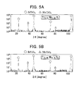
- X-ray diffraction (XRD) measurement of the metal oxide layer 12 was carried out when the Nb substitutional rate x was 0, 0.01, 0.02, and 0.03 in the transparent metal Nb:TiO 2 (chemical formula Ti 1-x Nb x O 2 ) prepared based on the above-described methods. The results are shown in Figs. 3A, 3B, 4A, and 4B. Similarly, an X-ray diffraction (XRD) measurement of the metal oxide layer 12 was carried out when the Nb substitutional rate x was changed with 0.06, 0.1, 0.15, and 0.2 in the transparent metal Nb:TiO 2 (chemical formula Ti 1-x Nb x O 2 ) prepared based on the above-described methods.
- the relationship of lattice constant and the Nb substitutional rate x in the prepared metal oxide layer 12 was determined based on XRD spectrums when the Nb substitutional rate x was 0, 0.01, 0.02, 0.03, 0.06, 0.1, 0,15, and 0.20. It is found that the lattice constant increases as the rate of addition of Nb increases. This result suggests that the prepared metal oxide layer 12 exists as what is known as a solid solution.
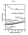
- the internal transmittance of the prepared metal oxide layer 12 when the Nb substitutional rate x was 0, 0.01, 0.02, 0.03, 0.06, 0.1, 0.15, and 0.2 was determined.
- the "transmittance" in an original meaning must consider that the amount of reflection is a deficiency, and then, when the amount of reflection in the metal oxide layer 12 is deducted, the transmittance used as 100% is hereinafter referred to "internal transmittance".
- the result is shown in Fig. 8. As shown in Fig. 8, the internal transmittance is 80% or greater in the visible light region (400 to 800 nm of wavelength) which is a satisfactory result.
- a sample having the Nb substitutional rate x being 0.06 or less made it possible to achieve internal transmittance being 95% or greater in the visible light region.
- the cause by which internal transmittance decreases as the Nb substitutional rate increases it is considered that the amount of Ti 3+ as well as Nb substitutional rate increase and transition probability between t 2g -e g bands each having an absorption edge in the visible light region increases.
- the thickness of the metal oxide layer 12 is 100 nm or greater in many cases, and especially, the specifications required in ITO now is 80% or greater internal transmittance to the film thickness 100nm or greater. 95% or greater internal transmittance to the film thickness 50nm is required for satisfying the specifications.
- a transparent conductor thin film which has higher internal transmittance than that of the conventional ITO thin film can be prepared.
- Fig. 9 shows the temperature dependency of the resistivity of the metal oxide layer 12 prepared with the above-described Nb substitutional rate.
- the metal oxide layer 12 in which the Nb substitutional rate x is 0.01 or greater and 0.2 or less has satisfactory conductivity at a level of 10 -4 ⁇ cm at room temperature in comparison with a metal oxide layer having no Nb.
- the present invention makes it possible that the transparent metal 1 according to the present invention has resistivity at a level of 10 -4 ⁇ cm when the Nb substitutional rate x is not only 0.01 or greater and 0.2 or less but is also 0,001 or greater and 0.2 or less.
- resistivity is decreased to 5 ⁇ 10 -4 ⁇ cm at room temperature (280 to 300K) and 1 ⁇ 10 -4 ⁇ cm at cryogenic temperature (5 to 20K) while internal transmittance is further improved.
- the present invention makes it possible that the transparent metal 1 according to the present invention has high transparency and low resistivity (conductivity at a level of 10 -4 ⁇ cm) almost equal to that of the ITO film in which Nb:TiO 2 obtained by substituting Nb for Ti of the anatase TiO 2 is used as the metal oxide layer 12.
- the Nb substitutional ratio of the metal oxide layer 12 is controlled so that the resistivity of the metal oxide layer 12 becomes 2 ⁇ 10 - 4 to 5 ⁇ 10 -4 ⁇ cm at room temperature or 8 ⁇ 10 -5 to 2 ⁇ 10 -4 ⁇ cm at cryogenic temperature, it becomes possible to remarkably extend applicability to various devices such as a liquid crystal panel.
- the X-ray diffraction (XRD) measurement of the metal oxide layer 12 was carried out when the Ta substitutional rate x was 0.002, 0.005, 0.15, and 0.20 in the transparent metal Ta:TiO 2 (chemical formula Ti 1-x Ta x O 2 ) prepared based on the above-described methods.
- the results are shown in Figs. 10A, 10B, 11A, and 11B. According to the XRD spectrums shown in Figs. 10A to 11B, these results confirmed that Ta:TiO 2 is stably generated without depending on the Ta substitutional rate like Nb:TiO 2 .
- Fig. 12 is a diagram showing a measurement result of temperature variations of carrier concentrations. Carrier concentrations were determined when the Ta substitutional rate was 0.005, 0.1, 0.03, 0.05, and 0.10. As shown in Fig. 12, the temperature dependency of the carrier concentration in any Ta substitutional rate did not appear. This means that Ta:TiO 2 is a degenerated semiconductor which is a property appearing in a transparent conductive film such as an ITO film.
- Fig. 13 is a diagram showing a measurement result of temperature variations of Hall mobilities. Hall mobilities were determined when the Ta substitutional rate was 0,005, 0.1, 0.03, 0.05, and 0.10. As shown in Fig, 13, Hall mobilities decreased with a temperature rise in any Ta substitutional rate, and reduction of Hall mobility became large as the Ta substitutional rate became small.
- the temperature dependency of Hall mobility is a property which is not observed in ITO, and that causes an increase of resistivity with a temperature rise. The derivation of temperature dependency is not clear now, however, an increase of resistivity with the temperature rise is a property which is observed in ordinary metals and thereby Ta:TiO 2 is called a transparent metal.
- the relationship of the lattice constant and the Ta substitutional rate x in the prepared metal oxide layer 12 was determined based on the XRD spectrum when the Nb substitutional rate x was 0.005, 0.1, 0.05, 0.10, 0.15, and 0.20. As shown in Fig. 14, it is found that lattice constant increases as the rate of addition ofNb increases, that is, it is found that lattice expands in accordance with Vegard's law (the linear relationship between the lattice constant and the composition of a solid solution alloy expressed with weight percentage). This result suggests that the prepared metal oxide layer 12 exists as what is known as a solid solution. In Fig. 14, triangles represent a-axis lattice constants and circles represent c-axis lattice constants.
- the transmittance of the metal oxide layer 12 prepared when the Ta substitutional rate x was 0.01, 0.03, 0.05, 0.10, 0.15, and 0.20 was determined. The result is shown in Fig. 15. As shown in Fig. 15, the transmittance is 60% or greater in the visible light region (400 to 800 nm of wavelength) which is a satisfactory result. In particular, a sample having the Ta substitutional rate x being 0.05 or less made it possible to achieve stable and high transmittance even if in the visible light long-wavelength region (red region).
- Fig. 16 shows the temperature dependency of the resistivity of the metal oxide layer 12 prepared with the above-described Ta substitutional rate.
- the metal oxide layer 12 in which the Ta substitutional rate x is 0.005 or greater and 0.2 or less has satisfactory conductivity at a level between 10 -4 ⁇ cm and 10 -3 ⁇ cm at room temperature.
- the Ta substitutional rate x is preferably 0.01 or greater and 0.1 or less.
- the Ta substitutional rate x is more preferably 0.03 or greater and 0.1 or less.
- Fig. 17 is a diagram showing the relationship of the amount of Ta doped and the resistivity/transmittance
- circles represent the resistivities and triangles represent the transmittances.
- a region being of small resistivity and large transmittance is the region of the Ta substitutional rate x being 0,03 or greater and 0.1 or less.
- a region being of smaller resistivity and larger transmittance is the region of Ta substitutional rate x being 0.05 or greater and 0.1 or less.
- the present invention makes it possible that the transparent metal 1 according to the present invention has resistivity at a level between 10 -4 ⁇ cm and 10 -3 ⁇ cm when the Ta substitutional rate x is not only 0.005 or greater and 0.2 or less but is also 0.001 or greater and 0.2 or less.
- the Ta substitutional rate x is 0.01 or greater and 0.05 or less in the metal oxide layer 12, stable and high transmittance is able to be achieved even if in the red region.
- resistivity is decreased to 5 ⁇ 10 -4 ⁇ cm at room temperature (280 to 300K) and 5 ⁇ 10 -5 to 2 ⁇ 10 -4 ⁇ cm at cryogenic temperature (5 to 20K) while stable and high transmittance is achieved even if in the red region.
- the present invention makes it possible that the transparent metal 1 according to the present invention has a high transparency and low resistivity almost equal to that of the ITO film in which Ta:TiO 2 obtained by substituting Ta for Ti of the anatase TiO 2 is used as the metal oxide layer 12.
- the Ta substitutional ratio of the metal oxide layer 12 is controlled so that the resistivity of the metal oxide layer 12 becomes 2 ⁇ 10 -4 to 1.8 ⁇ 10 -3 ⁇ cm at room temperature or 5 ⁇ 10 -5 to 7 ⁇ 10 -4 ⁇ cm at cryogenic temperature, it becomes possible to remarkably extend applicability to various devices such as a liquid crystal panel.
- transparent metal 1 can be applied to an electrode for a solar cell which uses TiO 2 as a photocatalyst in addition to application for an electrode of a conventional solar cell.
- Applying the transparent metal I having a low resistivity to a liquid crystal display panel causes reduction of the power consumption of the display device of the liquid crystal display panel, and therefore, enlargement and miniaturization for portability of the liquid crystal display panel can be accelerated. According to the above-described constitution, labor accompanying production is remarkably reduced in addition to cost reduction with facilitation of raw material acquisition and simplification of production processes using the transparent metal 1.
- the transparent metal 1 according to the present invention when used as an electrode, a transparent electrode having conventional performance can be produced at a low price and thereby applicability can be extended. Furthermore, since Nb:TiO 2 , Ta:TiO 2 , and the like which are not eroded by acid and alkali are used as the metal oxide layer 12 constituting the transparent metal 1, applicability can be extended without the influence of the ambient environment.
- the substrate 11 on which the metal oxide layer 12 is formed is defined as a transparent metal 1, however, the transparent metal 1 is not limited to this embodiment and the metal oxide layer 12 itself may be defined as a transparent metal 1.
- the transparent metal 1 according to the present invention is not limited to the use as an electrode and may be applied to a part, a thin film, a device, or the like which require transparency and high conductivity.
- Figs. 18A, 18B, and 18C show the Nb amount dependencies to mobility, scattering time of the carrier, and effective mass of the carrier of Ti 1-x Nb x O 2 single crystal thin film at room temperature.
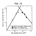
- Fig.19 shows a log-log graph showing a Nb concentration dependency of scattering time.
- the scattering (relaxation) time of the carrier rapidly increases with the increase of the Nb amount and gradually decreases from the point that the Nb substitutional amount x has achieved to 0.01. From the results of a ZnO thin film sample which is the same as a transparent conductor, it is considered that grain boundary scattering is dominant in x being less than 0.01 and scattering by neutral/ionized impurities is dominant in x being greater than 0.01 (see Fig. 19). As described above, regarding a sample having satisfactory carriers, since grain boundary scattering can be neglected even if the sample is a polycrystal sample, the polycrystal sample is able to maintain performance almost equal to that of the single crystal sample. This fact is a very advantageous point for developing an organic EL panel, a liquid crystal panel, or the like which necessarily use polycrystal thin films.
- the monotonical increase of the effective mass of carrier with the Nb amount suggests the decrease of curvature of the conductive band as the conductive band separates from the minimum of conduction band (variation is smaller than that of scattering time).
- the absolute value of variation is 0.2 to 0,4 m 0 (m 0 is the rest mass of an electron) and the value is almost equal to that of SnO 2 (0.2 to 0.3 m 0 ) or that of ITO (0.3 m 0 ).
- the tendency of mobility reflects the change of the Nb amount of scattering time in general. That is, the transport phenomenon at room temperature strongly depends on the change of a scattering mechanism with Nb addition rather than a band structure.
- the vicinity of x being 0.01 to 0.03 is the optimum composition in which both grain boundary scattering and impurity scattering can be suppressed to the minimum.
- metal oxide has the composition of Ti 1-x-y Nb x Ta y O 2 , the metal oxide can be sufficiently used until x+y becomes 0.3 by experimentation. As long as it is decided by X-ray measurement, it has been ascertained that x and y can be substituted to 40% (x+y is 0.4 or less). When it is desired that only blue-ultraviolet rays are transmitted even if transparency in the visible light region decreases, the metal oxide having a large substitutional ratio x+y is sufficiently used depending on use such as application to a heat reflecting film and thereby the maximum of x+y when Nb and Ta are mixed becomes larger.
- TiO 2 film may be provided by applying an oriented film being at least one selected from the group consisting of ZnO, ZrO 2 , SrTiO 3 , MgO, LaAlO 3 , CeO 2 , ZrO 2 , and Al 2 O 3 films on a substrate beforehand, and forming a TiO 2 film thereon.
- the oriented film acts as a buffer film (buffer layer),
- the buffer layer is important to form an anatase type film on glass. Since ZnO is easily oriented, there is an advantage that a ZnO film is easily formed.
- V, Mn, Tc, Re, P, Bi, and the like are applicable for using as a dopant which imparts transparent conductivity. All other elements have applicability for use as a dopant imparting transparent conductivity.
- transparent conductive materials are based on an oxide of Sn, In, or Zn, and oxide thin films such as ITO, SnO 2 , and ZnO are used as a transparent conductive film.
- Al or Ga is an effective dopant for a ZnO film.
- These elements are placed on the right side of the periodic table. It is known that these elements have an electric conduction mechanism based on an s electron or a p electron.
- electric conduction is imparted by a d electron, so the conductor is a new type of transparent conductor.
- the TiO 2 film may be grown on a GaN substrate.
- the present inventors have found that epitaxial growth of the TiO 2 film is performed on the GaN substrate. Concretely, the following composition is considered.
- Functional device characterized by comprising Al x Ga y In z N (0 ⁇ x ⁇ 1, 0 ⁇ y ⁇ 1, and 0 ⁇ z ⁇ 1) and an oxide material formed on the Al x Ga y In z N composed of a metal oxide which is TiO 2 .
- the metal oxide is doped with one or more elements selected from the group consisting of Nb, Ta, Mo, As, Sb, Al, and W.
- the metal oxide is doped with one or more elements selected from the group consisting of Co, Fe, Cr, Sn Ni, Mn, and V.
- the oxide material film may be formed by not only a PLD method, but also another physical vapor deposition (PVD) method such as a molecular beam epitaxy (MBE) method and a sputtering method, or a chemical vapor deposition (CVD) method, for example, a MOCVD method other than the PLD method.
- PVD physical vapor deposition
- MBE molecular beam epitaxy
- CVD chemical vapor deposition
- the oxide material can be used as an optical magnetic device showing a large Faraday rotation coefficient in the vicinity of a wavelength of 400 nm. Especially, since a large Faraday rotation coefficient equal to that of a magnetic garnet film is obtained, an optical isolator suitable for a next generation short wavelength region communication can be prepared using the oxide material.
- the oxide material can be used for a magneto-optical device such as an optical circulator, a variable optical attenuator, an optical communication device, or the like; a magneto-optical device: an optical circuit; a nonreciprocal optical part; a nonreciprocal optical element; a semiconductor laser equipped with an isolator; a current-magnetic field sensor; a magnetic domain observation; a magneto-optical measurement; or the like.
- optical isolator typical examples include a module comprising an LD and an isolator to be a unit; an optical isolator for fiber insertion; an optical isolator for an optical amplifier; a deflection-dependent type optical isolator, a deflection-independent type optical isolator; and an optical waveguide type optical isolator.
- optical waveguide optical isolator typical examples include a Mach-Zehnder type branching waveguide isolator and a rib type waveguide isolator.
- a deflection-dependent type circulator and a deflection-independent type circulator may be used.
- an optical isolator which also corresponds to a short wavelength region such as blue or ultraviolet is able to be achieved. If the optical isolator is formed on the TiO 2 film with epitaxial growth, a functional device is monolithically obtained as well as the TiO 2 film acts as a buffer for crystal growth. That is, development of a monolithic functional device as well as a highly efficient light emitting device and a display with a low-cost and a large area can be carried out. For example, the fusion of a transparent electrode and an optical device, and the fusion of a light emitting device and a magneto-optical device can be achieved.
- the oxide material may be used for a light receiving element, a high frequency device such as a HEMT (high electron mobility transistor) or the like, and an electronic device.
- an electrode for a dye sensitized solar cell a display panel, an organic EL panel, a light emitting element, a light emitting diode (LED), a transparent electrode of white LED or blue laser (film forming on the GaN), a transparent electrode for a vertical cavity surface emitting laser, a lighting device, a communication device, and an application that only blue light is made to transmit
- the transmittance is preferably 90% or greater in the visible light region and a long wavelength red light region may be filtered to pass only blue light.
- the thin layer doped with a large amount ofNb is effective in this case. It is not essential that transmittance becomes 90% or greater.
- the doping amount ofNb or the like is simply adjusted in accordance with the application or a balance between resistivity and transmittance.
- the GaN compound may include not only GaN but also GaN with a small amount of dopant.
- the transparent metal 1 examples include a transparent conductive film on a liquid crystal display (LCD), a transparent conductive film on a color filter part, a transparent conductive film on an electro luminescence (EL) display, a transparent conductive film on a plasma display panel (PDP), a PDP optical filter, a transparent conductive film for blocking electromagnetic waves, a transparent conductive film for blocking a near infrared ray, a transparent conductive film for preventing surface reflection, an optical filter, a touch panel, a resistive type touch panel, an electromagnetic induction type touch panel, an ultrasonic type touch panel, an optical touch panel, an electrical capacitance type touch panel, a resistive type touch panel for personal digital assistants, a touch panel unified with a display (inner touch panel), a solar cell, an amorphous (a-Si) solar cell, a microcrystalline Si thin film solar cell, a CIGS solar cell, a dye sensitized solar cell (
- a substrate for transparent electrode having transparency and conductivity is achieved and the substrate is able to be applied in various uses.
Abstract

Description
- The present invention relates to a transparent conductor to be applied for a liquid crystal panel, a solar cell, an organic electroluminescence (EL) electrode, and the like.
- In recent years, needs for enlargement of liquid crystal display panels and needs for smaller-size and portability have risen. In order to achieve these, low power consumption of a display device is required and it is necessary to apply a transparent electrode having high visible light transmittance and low resistance value.
- Particularly, an organic electroluminescence (EL) device developed recently is a self-luminous type device and can be effectively applied to a small portable device, however, there are problems in which the organic EL device is a current driven device and has a large power consumption. Furthermore, a plasma display panel (PDP) which is spreading in the market recently and a field emission display (FED) currently developed as a next-generation display have a problem in that they have high power consumption structures. Therefore, a low resistance-transparent conductive thin film is greatly expected.
- In order to decrease the resistance value of the transparent conductive thin film, the transparent conductive thin film in which an indium tin oxide film (hereinafter referred to as ITO film) consisting of indium oxide doped with tin within a certain percentage is provided on the surface of a transparent substrate such as a glass plate or the like is proposed (for example, patent document 1).
- The ITO film has superior transparency and high conductivity, however, there are problems that the content of indium in the earth crust is very low 50 ppb and the cost of raw materials increases as resources are exhausted.
- In recent years, a zinc oxide material has been proposed as a low-priced material having high plasma resistance.
- However, since the zinc oxide material is weak to acid or alkali, and is gradually eroded in a carbon dioxide atmosphere, particularly, application to a solar cell becomes difficult as well as application to a liquid crystal panel. Even if it is considered that the surface of the zinc oxide is treated by a coating process in order to improve the chemical resistance, adding a process for coating causes an increase in production cost.
- For enlarging applicability of the transparent conductor, it is required that the transparent conductor consists of raw materials which can be stably supplied and have chemical resistance and durability in combination.
Patent Document 1:Japanese Unexamined Patent Application, First Publication 2004-095240 - The present invention was made in view of the above-described background technology. Its object is to provide a transparent conductor having transparency and conductivity which is capable of being stably supplied and is composed of raw materials with superior chemical resistance.
- The first aspect of the present invention is a transparent conductor including a metal oxide characterized in that the metal oxide is M:TiO2 having an anatase type crystal structure.
- The second aspect of the present invention is a transparent conductor including a metal oxide characterized in that the metal oxide is a M:TiO2 having an anatase type crystal structure (M is one selected from the group consisting ofNb, Ta, Mo, As, Sb and W).
- The third aspect of the present invention is a transparent conductor including a metal oxide characterized in that the metal oxide is a M:TiO2 having an anatase type crystal structure (M is one selected from the group consisting of V, Mn, Tc, Re, P, and Bi).
- The fourth aspect of the present invention is a transparent conductor including a metal oxide characterized in that the metal oxide is a M:TiO2 having an anatase type crystal structure (M is one selected from the group consisting ofTa and Nb).
- The fifth aspect of the present invention is a transparent conductor according to the first aspect characterized in that the metal oxide also has metallic electric conductivity.
- The sixth aspect of the present invention is a transparent conductor according to the fourth aspect characterized in that the metal oxide is represented by the formula Ti1-xNbxO2 (0.001 ≤ x ≤ 0.2).
- The seventh aspect of the present invention is a transparent conductor according to the fourth aspect characterized in that the metal oxide is represented by the formula Ti1-xNbxO2 (0.01 ≤ x ≤ 0.2).
- The eighth aspect of the present invention is a transparent conductor according to the fourth aspect characterized in that the metal oxide is represented by the formula Ti1-xNbxO2 (0.01 ≤ x ≤ 0.03).
- The ninth aspect of the present invention is a transparent conductor according to the fourth aspect characterized in that the metal oxide is represented by the formula Ti1-xNbxO2 (0.01 ≤ x ≤ 0.6).
- The tenth aspect of the present invention is a transparent conductor according to the fourth aspect characterized in that the metal oxide is represented by the formula Ti1-xNbxO2 (0.02 ≤ x ≤ 0.6).
- The eleventh aspect of the present invention is a transparent conductor according to the fourth aspect characterized in that the metal oxide is represented by the formula Ti1-xTaxO2 (0.001 ≤ x ≤ 0.2).
- The twelfth aspect of the present invention is a transparent conductor according to the fourth aspect characterized in that the metal oxide is represented by the formula Ti1-xTaxO2 (0.005 ≤ x ≤ 0.2).
- The thirteenth aspect of the present invention is a transparent conductor according to the fourth aspect characterized in that the metal oxide is represented by the formula Ti1-xTaxO2 (0.01 ≤ x ≤ 0.1).
- The fourteenth aspect of the present invention is a transparent conductor according to the fourth aspect characterized in that the metal oxide is represented by the formula Ti1-xTaxO2 (0.03 ≤ x ≤ 0.1).
- The fifteenth aspect of the present invention is a transparent conductor according to the fourth aspect characterized in that the metal oxide is represented by the formula Ti1-xTaxO2 (0.05 ≤ x ≤0.1).
- The sixteenth aspect of the present invention is a transparent conductor according to the fourth aspect characterized in that the metal oxide is represented by the formula Ti1-x-yNbxTayO2 (0 ≤ x+y ≤ 0.4).
- The seventeenth aspect of the present invention is a transparent conductor according to the fourth aspect characterized in that the metal oxide is represented by the formula Ti1-x-yNbxTayO2 (0 ≤ x+y ≤ 0.3).
- The eighteenth aspect of the present invention is the transparent conductor according to the first aspect characterized in that the metal oxide is provided on a perovskite type crystal substrate.
- The nineteenth aspect of the present invention is the transparent conductor according to the fourth aspect characterized in that the metal oxide has resistivity of 2 × 10⁻⁴ to 5 × 10⁻⁴ Ωcm at room temperature or 8 × 10⁻⁵ to 2 × 10⁻⁴ Ωcm at cryogenic temperature.
- The twentieth aspect of the present invention is the transparent conductor according to the fourth aspect characterized in that the metal oxide has resistivity of 2 × 10⁻⁴ to 1.8 × 10⁻³ Ωcm at room temperature or 5 × 10⁻⁵ to 7 × 10⁻⁴ Ωcm at cryogenic temperature.
- The twenty-first aspect of the present invention is a transparent electrode comprising the transparent conductor according to the first aspect.
- The twenty-second aspect of the present invention is the transparent conductor according to the first aspect characterized in that the metal oxide is provided to a GaN compound film.
- The twenty-third aspect of the present invention is the transparent conductor according to the first aspect characterized in that the metal oxide is provided to an oriented film which is provided to a substrate.
- The twenty-fourth aspect of the present invention is the transparent conductor according to the twenty-third aspect characterized in that the oriented film is at least one selected from the group consisting of ZnO, ZrO2, SrTiO3, MgO, LaAlO3, CeO2, ZrO2, and Al2O3 films.
- The twenty-fifth aspect of the present invention is the transparent conductor according to the twenty-third aspect characterized in that the oriented film is a ZnO film.
- The twenty-sixth aspect of the present invention is the transparent conductor according to the first aspect characterized in that a d electron imparts electric conductivity.
- The twenty-seventh aspect of the present invention is a solar cell comprising the transparent conductor according to the first aspect.
- The twenty-eighth aspect of the present invention is a light emitting device comprising the transparent conductor according to the first aspect.
- The twenty-ninth aspect of the present invention is a display panel comprising the transparent conductor according to the first aspect.
- The present invention enables a remarkable increase of the electric conductivity while maintaining the transparency by using M:TiO2 obtained by replacing Ti site of an anatase type TiO2 with another metal atom (Nb, Ta, Mo, As, Sb, W, or the like) or the like. The crystalline form of the M:TiO2 may a single crystal or a polycrystal,
- Particularly, when the Nb substitution is 0.1 to 20% as the ratio of the number of Nb and Ti atoms (Nb/Ti) in the metal oxide, it becomes possible to suppress the resistivity to a level of 10-4 Ωcm.
- When the Nb substitution is 1 to 20% as the ratio of the number of Nb and Ti atoms (Nb/Ti) in the metal oxide, it becomes possible to suppress the resistivity to a level of 10-4 Ωcm while the internal transmittance is maintained at a high level.
- When the Nb substitution is 1 to 6% as the ratio of the number ofNb and Ti atoms (Nb/Ti) in the metal oxide, it becomes possible to improve the internal transmittance to 95 to 98% (when the metal oxide is formed to a thin film as a sample and the thickness of the film is approximately 50 nm).
- When the Nb substitution is 2 to 6% as the ratio of the number of Nb and Ti atoms (Nb/Ti) in the metal oxide, it becomes possible to suppress the resistivity to approximately 5 × 10⁻⁴ Ωcm at room temperature and 1 × 10⁻⁴ Ωcm at cryogenic temperature (approximately 5K) while the internal transmittance is further improved,
- Furthermore, when the Ta substitution is 0.1 to 20% as the ratio of the number of Ta and Ti atoms (Ta/Ti) in the metal oxide, it becomes possible to suppress the resistivity to a level between 10-4 Ωcm and 10-3 Ωcm.
- When the Ta substitution is 0.5 to 20% as the ratio of the number of Ta and Ti atoms (Ta/Ti) in the metal oxide, it becomes possible to suppress the resistivity to a level between 10-4Ωcm and 10-3 Ωcm while the internal transmittance is maintained at a high level.
When the Ta substitution is 1 to 5% as the ratio of the number of Ta and Ti atoms (Ta/Ti) in the metal oxide, it becomes possible to stably obtain high internal transmittance even if red light is used. - When the Ta substitution is 1 to 3% as the ratio of the number of Ta and Ti atoms (Ta/Ti) in the metal oxide, it becomes possible to suppress the resistivity to approximately 5 × 10⁻⁴ Ωcm at room temperature and 1 × 10⁻⁴ to 2 × 10⁻⁴ Ωcm at cryogenic temperature while high internal transmittance is stably obtained even if red light is used.
- By providing (forming) the metal oxide to the perovskite type crystal substrate, it becomes possible to generate the anatase type crystal structure further selectively.
- By setting the resistivity of the metal oxide to 2 × 10⁻⁴ to 5 × 10⁻⁴ Ωcm at room temperature or 8 × 10⁻⁵ to 2 × 10⁻⁴ Ωcm at cryogenic temperature, or to 3 × 10⁻⁴ to 1.8 × 10⁻³ Ωcm at room temperature or 5 × 10⁻⁵ to 7 × 10⁻⁴ Ωcm at cryogenic temperature, it becomes possible to remarkably extend applicability for various devices such as a display panel. According to the present invention, particularly, enlargement of area and mass production of the transparent conductor are carried out using the TiO2 film deposition technique. Therefore, a substrate for transparent electrodes is able to be applied to an electrode for a solar cell which uses TiO2 as a photocatalyst in addition to application for an electrode of a conventional solar cell. Applying the substrate for transparent electrodes to a liquid crystal display panel causes a reduction of the power consumption of a display device of the liquid crystal display panel, and therefore, enlargement and miniaturization for portability of the liquid crystal display panel are accelerated.
- According to the above-described constitution in the present invention, the labor accompanying production is remarkably reduced in addition to cost reduction with facilitation of raw material acquisition and simplification of production processes.
- Since TiO2 having high durability to chemicals and outside air is used as a parent material in the present invention, it becomes possible to extend applicability to solar cells to be expected with the usage in field. Furthermore, since a coating process is not required, cost reduction with a decrease of the number of processes is achieved.
- Other objects, characteristics, and advantages of the present invention will be described by the detailed description with reference to the following best mode for carrying out the invention and attached drawings.
-
- Fig. 1 is a diagram showing a substrate for a transparent electrode formed by laminating metal oxide layers on the substrate.
- Fig. 2 is a diagram for explaining the structure of a PLD device.
- Fig. 3A is a diagram showing the result of an X-ray diffraction measurement of metal oxide layers.
- Fig. 3B is a diagram showing the result of an X-ray diffraction measurement of a metal oxide layer.
- Fig. 4A is a diagram showing the result of an X-ray diffraction measurement of a metal oxide layer.
- Fig. 4B is a diagram showing the result of an X-ray diffraction measurement of a metal oxide layer.
- Fig. 5A is a diagram showing the result of an X-ray diffraction measurement of a metal oxide layer.
- Fig. 5B is a diagram showing the result of an X-ray diffraction measurement of a metal oxide layer.
- Fig. 6A is a diagram showing the result of an X-ray diffraction measurement of a metal oxide layer.
- Fig. 6B is a diagram showing the result of an X-ray diffraction measurement of a metal oxide layer.
- Fig. 7 is a diagram showing the result of a lattice constant measurement of metal oxide layers.
- Fig. 8 is a diagram showing the result of the internal transmittance measurement of prepared metal oxide layers.
- Fig. 9 is a diagram showing a temperature dependency to resistivity of prepared metal oxide layers.
- Fig. 10A is a diagram showing the result of an X-ray diffraction measurement of a metal oxide layer.
- Fig. 10B is a diagram showing the result of an X-ray diffraction measurement of a metal oxide layer,
- Fig. 11A is a diagram showing the result of an X-ray diffraction measurement of a metal oxide layer.
- Fig. 11B is a diagram showing the result of an X-ray diffraction measurement of a metal oxide layer.
- Fig. 12 is a diagram showing a measurement result of temperature variations of carrier concentrations of metal oxide layers.
- Fig. 13 is a diagram showing a measurement result of temperature variations of Hall mobilities of metal oxide layers.
- Fig. 14 is a diagram showing a measurement result of lattice constant of metal oxide layers.
- Fig. 15 is a diagram showing a measurement result of transmittance of metal oxide layers.
- Fig. 16 is a diagram showing temperature dependencies of resistivities of prepared metal oxide layers.
- Fig, 17 is a diagram showing the relationship of Ta-doped amount and resistivity/transmittance.
- Fig. 18A is a diagram showing a Nb amount dependency to mobility of Ti1-xNbxO2 single crystal thin layers at room temperature,
- Fig. 18B is a diagram showing a Nb amount dependency to the scattering time of carriers of Ti1-xNbxO2 single crystal thin layers at room temperature.
- Fig. 18C is a diagram showing a Nb amount dependency to the effective mass of carriers of Ti1-xNbxO2 single crystal thin layers at room temperature.
- Fig. 19 is a diagram of a log-log graph showing a Nb concentration dependency of scattering time.
-
- 1
- Transparent metal
- 11
- Substrate
- 12
- Metal oxide layer
- 30
- PLD device
- 31
- Chamber
- 32
- Light emitter
- 33
- Reflecting mirror
- 34
- Lens
- 36
- Infrared lump
- 39
- Target
- 40
- Oil-sealed rotary pump
- 41
- Back-flow preventing valve
- 42
- Turbo molecular pump
- 43
- Pressure valve
- 45
- Oxygen gas flow rate regulating valve
- Embodiments of the present invention are explained in detail with reference to drawings.
- The present invention is applied for use as a transparent metal (transparent conductor) 1 to be applied to electrodes of display panels, organic ELs, solar cells, or the like. The present invention comprises a
metal oxide layer 12 formed on asubstrate 11 as a polycrystal or single crystal as shown in Fig. 1. - The
transparent metal 1 shows metallic electric conductivity in the transparent conductor until the cryogenic temperature (5K) in which the metallic electric conductivity is defined to have 10-2 Ωcm or less of resistivity at room temperature and dR/dT > 0 (R: resistivity, T: temperature) of temperature dependency of resistivity. The metallic electric conductivity preferably has 10-3 Ωcm or less resistivity at room temperature in view of increasing general use. - The
substrate 11 is composed of strontium titanate (SrTiO3) formed so that a substrate surface 11a is a (100) plane. - The
substrate 11 may be composed of a SrTiO3 single crystal substrate, or may be composed of any material as long as the material is another perovskite type crystal or a rock type crystal containing similar structure thereto. That is, when thesubstrate 11 is composed of perovskite type or rock type crystal, an anatase single crystal thin layer can be formed. - The
substrate 11 may be composed of an amorphous material such as glass, quartz, or plastic. In this case, an anatase polycrystal thin layer is formed, however, it hardly affects fundamental physical properties such as resistivity. - Although the thickness of the
substrate 11 is not limited to 50 nm, as described in the following embodiment, the thickness is, for example, preferably 1000 nm or less. The thickness may be greater than 1000 nm ifsubstrate 11 is required to have lower resistance and is allowed to have slightly lower transmittance. - The
metal oxide layer 12 formed by laminating on thesubstrate 11 is composed of Nb:TiO2. Nb:TiO2 is formed by substituting Nb for Ti of the anatase TiO2. Nb may be replaced with, for example, Ta, Mo, As, Sb, or W. Another element may also be used. Themetal oxide layer 12 is formed on a substrate surface 12a with epitaxial growth. The thickness of themetal oxide layer 12 is preferably 40 to 50 nm, however, the thickness is not limited to this range. - Next, a method for preparing
transparent metal 1 is explained. - First, a SrTiO3 substrate which is cut so that the substrate surface becomes a (100) plane is mechanically polished using, for example, a diamond slurry. In the mechanical polishing, the particle size of the diamond slurry used is gradually made finer and lastly, mirror polishing is carried out with approximately 0.5 µm of the particle size of the diamond slurry. After the mirror polishing, the surface of SrTiO3 substrate may be flattened by further polishing with colloidal silica until the RMS of the surface roughness becomes 10 Å or less.
- Next, Nb:TiO2 is deposited on the SrTiO3 (100) plane of the
substrate 11 by a physical vapor deposition (PVD) process. Hereinafter, the case that the deposition is performed by a pulsed laser deposition (PLD) process is explained. - In the PLD process, the
metal oxide layer 12 is deposited on thesubstrate 11 using aPLD device 30 as shown in Fig. 2. ThePLD device 30 comprises achamber 31, thesubstrate 11 and atarget 39 provided in thechamber 31, alight emitter 32 which is provided opposite to the surface of thetarget 39 outside thechamber 31, a reflecting mirror 33 for adjusting the position of a pulsed laser light emitted from thelight emitter 32 provided outside thechamber 31, alens 34 for controlling a spot diameter of a laser beam provided outside thechamber 31, and agas supply device 44 for injecting oxygen gas into thechamber 31 provided outside thechamber 31. - The
chamber 31 is provided for preparing a high quality thin film by maintaining an appropriate degree of vacuum and, concurrently, by preventing contamination from the outside. In thechamber 31, aninfrared lump 36 is provided for heating a substrate. The temperature of substrate is monitored by aradiation thermometer 37 provided outside thechamber 31 via awindow 31b and is controlled so as to always be a constant temperature, Furthermore, avalve 45 for regulating the flow rate of oxygen gas is provided in thechamber 31. In order to achieve film deposition under reduced pressure, thechamber 31 is connected with a turbomolecular pump 42 and apressure valve 43. The pressure of thechamber 31 is controlled by the oxygen gas flowrate regulating valve 45 and thepressure valve 43 so as to be 10-5 to 1 × 10⁻⁴ torr in, for example, an oxygen atmosphere. The turbomolecular pump 42 is connected with an oil-sealedrotary pump 40 and a back-flow preventing valve 41 and the pressure at the exhaust side of the turbomolecular pump 42 is always maintained so as to be 10-4 torr or less. - A window 31 a is further provided at the surface of the
chamber 31 which is opposite to thetarget 39. Thelight emitter 32 emits the pulsed laser light incident on thechamber 31 via the window 31a. Thelight emitter 32 emits a KrF excimer laser having, for example, 1 to 10 Hz of pulse frequency, 50 mJ/pulse of laser power, and 248 nm of wavelength as the above-described pulsed laser light. The emitted pulsed laser light is spot-adjusted so that the focal position is near thetarget 39 by the reflecting mirror 33 and thelens 34, and incidence is carried out at an angle of approximately 45° to the surface of thetarget 39 provided in thechamber 31 via the window 31a. - The
target 39 is composed of, for example, a Nb:TiO2 sintered body. The metal to be substituted is Nb as an example in this embodiment, however, any one of Ta, Mo, As, Sb, and W may be used or plural kinds of metals may be combined. The Nb:TiO2 sintered body is prepared by mixing TiO2 powder and Nb2O5 powder which are weighed so as to be a desired atomic ratio and further heat-molding the mixed powder. Thetarget 39 is provided to be parallel to the (100) plane of thesubstrate 11. - The film deposition process based on the PLD method is explained below.
- The
substrate 11 which is polished is provided in thechamber 31. Next, thesubstrate 11 is annealed under an oxygen atmosphere of 10-5 Torr at 650°C substrate temperature in order to remove impurities on the surface of thesubstrate 11 and flatten the surface at an atomic level. At least one hour is required as the annealing time. - The
substrate 11 is driven with rotation by motor 35 under anoxygen atmosphere 10-5 Torr at 550°C of substrate temperature to deposit a film. The above-described pulsed laser light is intermittently irradiated to thetarget 39 while thetarget 39 is driven with rotation via arotation axis 38, and thereby the surface temperature of thetarget 39 is rapidly increased and ablation plasma is generated. Each atom of Ti, Nb, and O included in the ablation plasma migrates to thesubstrate 11 while gradually changing conditions by repeating the collisional reaction or the like with oxygen gas in thechamber 31. Particles including Ti, Nb, or O atoms arrived at thesubstrate 11 diffuse the (100) plane on thesubstrate 11 as it is, and a thin film is formed in the stablest condition in lattice matching. As a result, thetransparent metal 1 composed of the above-described constitution is prepared. - The
transparent metal 1 may be prepared by not only the PLD method described above but also, for example, other physical vapor deposition (PVD) methods such as a molecular beam epitaxy method (MBE), a sputtering method, and the like, or a method other than PLD methods such as chemical vapor deposition (CVD) methods using, for example, an MOCVD method. Thetransparent metal 1 may also be prepared by a synthetic process from a solution such as a sol-gel method, a chemical solution method, and the like. - An X-ray diffraction (XRD) measurement of the
metal oxide layer 12 was carried out when the Nb substitutional rate x was 0, 0.01, 0.02, and 0.03 in the transparent metal Nb:TiO2 (chemical formula Ti1-xNbxO2) prepared based on the above-described methods. The results are shown in Figs. 3A, 3B, 4A, and 4B. Similarly, an X-ray diffraction (XRD) measurement of themetal oxide layer 12 was carried out when the Nb substitutional rate x was changed with 0.06, 0.1, 0.15, and 0.2 in the transparent metal Nb:TiO2 (chemical formula Ti1-xNbxO2) prepared based on the above-described methods. The results are shown in Figs. 5A, 5B, 6A, and 6B. According to the XRD spectrums shown in Figs. 3A to 6B, SrTiO3 peaks represented by circles in the figures appear at 2θ= 23.1°, 46.8°, 72.6°, 104.2°. The Nb:TiO2 peaks represented by triangles in the figures appear at 2θ= 37.8° and 80.4°. Therefore, these results confirmed that Nb:TiO2 is stably generated without depending on the Nb substitutional rate. - The relationship of lattice constant and the Nb substitutional rate x in the prepared
metal oxide layer 12 was determined based on XRD spectrums when the Nb substitutional rate x was 0, 0.01, 0.02, 0.03, 0.06, 0.1, 0,15, and 0.20. It is found that the lattice constant increases as the rate of addition of Nb increases. This result suggests that the preparedmetal oxide layer 12 exists as what is known as a solid solution. - The internal transmittance of the prepared
metal oxide layer 12 when the Nb substitutional rate x was 0, 0.01, 0.02, 0.03, 0.06, 0.1, 0.15, and 0.2 was determined. The "transmittance" in an original meaning must consider that the amount of reflection is a deficiency, and then, when the amount of reflection in themetal oxide layer 12 is deducted, the transmittance used as 100% is hereinafter referred to "internal transmittance". The result is shown in Fig. 8. As shown in Fig. 8, the internal transmittance is 80% or greater in the visible light region (400 to 800 nm of wavelength) which is a satisfactory result. In particular, a sample having the Nb substitutional rate x being 0.06 or less made it possible to achieve internal transmittance being 95% or greater in the visible light region. On the other hand, as the cause by which internal transmittance decreases as the Nb substitutional rate increases, it is considered that the amount of Ti3+ as well as Nb substitutional rate increase and transition probability between t2g-eg bands each having an absorption edge in the visible light region increases. - When the
metal oxide layer 12 is actually applied to a device, the thickness of themetal oxide layer 12 is 100 nm or greater in many cases, and especially, the specifications required in ITO now is 80% or greater internal transmittance to the film thickness 100nm or greater. 95% or greater internal transmittance to the film thickness 50nm is required for satisfying the specifications. As shown in Fig. 8, since suppressing the Nb substitutional rate to x being 0.06 or less satisfies the above-described specifications, a transparent conductor thin film which has higher internal transmittance than that of the conventional ITO thin film can be prepared. - Fig. 9 shows the temperature dependency of the resistivity of the
metal oxide layer 12 prepared with the above-described Nb substitutional rate. As shown in Fig. 9, themetal oxide layer 12 in which the Nb substitutional rate x is 0.01 or greater and 0.2 or less has satisfactory conductivity at a level of 10-4 Ωcm at room temperature in comparison with a metal oxide layer having no Nb. - The present invention makes it possible that the
transparent metal 1 according to the present invention has resistivity at a level of 10-4 Ωcm when the Nb substitutional rate x is not only 0.01 or greater and 0.2 or less but is also 0,001 or greater and 0.2 or less. - When the Nb substitutional ratio x is 0.01 or greater and 0.06 or less in the
metal oxide layer 12, internal transmittance is improved to 95 to 98% with a film thickness of 50 nm and 80% or greater with a film thickness of 100 nm. - When the Nb substitutional ratio x is 0.02 or greater and 0.06 or less in the
metal oxide layer 12, resistivity is decreased to 5 × 10⁻⁴ Ωcm at room temperature (280 to 300K) and 1 × 10⁻⁴ Ωcm at cryogenic temperature (5 to 20K) while internal transmittance is further improved. - The present invention makes it possible that the
transparent metal 1 according to the present invention has high transparency and low resistivity (conductivity at a level of 10-4 Ωcm) almost equal to that of the ITO film in which Nb:TiO2 obtained by substituting Nb for Ti of the anatase TiO2 is used as themetal oxide layer 12. - If the Nb substitutional ratio of the
metal oxide layer 12 is controlled so that the resistivity of themetal oxide layer 12 becomes 2 × 10 -4 to 5 × 10⁻⁴ Ωcm at room temperature or 8 × 10⁻⁵ to 2 × 10⁻⁴ Ωcm at cryogenic temperature, it becomes possible to remarkably extend applicability to various devices such as a liquid crystal panel. - The X-ray diffraction (XRD) measurement of the
metal oxide layer 12 was carried out when the Ta substitutional rate x was 0.002, 0.005, 0.15, and 0.20 in the transparent metal Ta:TiO2 (chemical formula Ti1-xTaxO2) prepared based on the above-described methods. The results are shown in Figs. 10A, 10B, 11A, and 11B. According to the XRD spectrums shown in Figs. 10A to 11B, these results confirmed that Ta:TiO2 is stably generated without depending on the Ta substitutional rate like Nb:TiO2. - Fig. 12 is a diagram showing a measurement result of temperature variations of carrier concentrations. Carrier concentrations were determined when the Ta substitutional rate was 0.005, 0.1, 0.03, 0.05, and 0.10. As shown in Fig. 12, the temperature dependency of the carrier concentration in any Ta substitutional rate did not appear. This means that Ta:TiO2 is a degenerated semiconductor which is a property appearing in a transparent conductive film such as an ITO film.
- Fig. 13 is a diagram showing a measurement result of temperature variations of Hall mobilities. Hall mobilities were determined when the Ta substitutional rate was 0,005, 0.1, 0.03, 0.05, and 0.10. As shown in Fig, 13, Hall mobilities decreased with a temperature rise in any Ta substitutional rate, and reduction of Hall mobility became large as the Ta substitutional rate became small. The temperature dependency of Hall mobility is a property which is not observed in ITO, and that causes an increase of resistivity with a temperature rise. The derivation of temperature dependency is not clear now, however, an increase of resistivity with the temperature rise is a property which is observed in ordinary metals and thereby Ta:TiO2 is called a transparent metal.
- The relationship of the lattice constant and the Ta substitutional rate x in the prepared
metal oxide layer 12 was determined based on the XRD spectrum when the Nb substitutional rate x was 0.005, 0.1, 0.05, 0.10, 0.15, and 0.20. As shown in Fig. 14, it is found that lattice constant increases as the rate of addition ofNb increases, that is, it is found that lattice expands in accordance with Vegard's law (the linear relationship between the lattice constant and the composition of a solid solution alloy expressed with weight percentage). This result suggests that the preparedmetal oxide layer 12 exists as what is known as a solid solution. In Fig. 14, triangles represent a-axis lattice constants and circles represent c-axis lattice constants. - The transmittance of the
metal oxide layer 12 prepared when the Ta substitutional rate x was 0.01, 0.03, 0.05, 0.10, 0.15, and 0.20 was determined. The result is shown in Fig. 15. As shown in Fig. 15, the transmittance is 60% or greater in the visible light region (400 to 800 nm of wavelength) which is a satisfactory result. In particular, a sample having the Ta substitutional rate x being 0.05 or less made it possible to achieve stable and high transmittance even if in the visible light long-wavelength region (red region). On the other hand, as the cause by which transmittance decreases as the Ta substitutional rate increases, it is considered that the amount of Ti3+ as well as the Ta substitutional rate increase and the transition probability between t2g-eg bands each having an absorption edge in the visible light region increases. - Fig. 16 shows the temperature dependency of the resistivity of the
metal oxide layer 12 prepared with the above-described Ta substitutional rate. As shown in Fig. 16, themetal oxide layer 12 in which the Ta substitutional rate x is 0.005 or greater and 0.2 or less has satisfactory conductivity at a level between 10-4 Ωcm and 10-3 Ωcm at room temperature. In view of further satisfactory conductivity, the Ta substitutional rate x is preferably 0.01 or greater and 0.1 or less. In view of satisfactory conductivity in a wide range from cryogenic temperature to room temperature, the Ta substitutional rate x is more preferably 0.03 or greater and 0.1 or less. - Fig. 17 is a diagram showing the relationship of the amount of Ta doped and the resistivity/transmittance, In Fig. 17, circles represent the resistivities and triangles represent the transmittances. As shown in Fig. 17, a region being of small resistivity and large transmittance is the region of the Ta substitutional rate x being 0,03 or greater and 0.1 or less. Furthermore, a region being of smaller resistivity and larger transmittance is the region of Ta substitutional rate x being 0.05 or greater and 0.1 or less. These regions indicate the optimum area of the amount of Ta doped.
- The present invention makes it possible that the
transparent metal 1 according to the present invention has resistivity at a level between 10-4 Ωcm and 10-3 Ωcm when the Ta substitutional rate x is not only 0.005 or greater and 0.2 or less but is also 0.001 or greater and 0.2 or less. - When the Ta substitutional rate x is 0.01 or greater and 0.05 or less in the
metal oxide layer 12, stable and high transmittance is able to be achieved even if in the red region. - When the Ta substitutional rate x is 0.01 or greater and 0.05 or less in the
metal oxide layer 12, resistivity is decreased to 5 × 10⁻⁴ Ωcm at room temperature (280 to 300K) and 5 × 10⁻⁵ to 2 × 10⁻⁴ Ωcm at cryogenic temperature (5 to 20K) while stable and high transmittance is achieved even if in the red region. - The present invention makes it possible that the
transparent metal 1 according to the present invention has a high transparency and low resistivity almost equal to that of the ITO film in which Ta:TiO2 obtained by substituting Ta for Ti of the anatase TiO2 is used as themetal oxide layer 12. - If the Ta substitutional ratio of the
metal oxide layer 12 is controlled so that the resistivity of themetal oxide layer 12 becomes 2 × 10⁻⁴ to 1.8 × 10⁻³ Ωcm at room temperature or 5 × 10⁻⁵ to 7 × 10⁻⁴ Ωcm at cryogenic temperature, it becomes possible to remarkably extend applicability to various devices such as a liquid crystal panel. - If the TiO2 film deposition technique which is applied to a photocatalyst or the like is used, it becomes possible to perform the enlargement of an area and the mass production of the
transparent metal 1. Therefore,transparent metal 1 can be applied to an electrode for a solar cell which uses TiO2 as a photocatalyst in addition to application for an electrode of a conventional solar cell. Applying the transparent metal I having a low resistivity to a liquid crystal display panel causes reduction of the power consumption of the display device of the liquid crystal display panel, and therefore, enlargement and miniaturization for portability of the liquid crystal display panel can be accelerated. According to the above-described constitution, labor accompanying production is remarkably reduced in addition to cost reduction with facilitation of raw material acquisition and simplification of production processes using thetransparent metal 1. - Therefore, when the
transparent metal 1 according to the present invention is used as an electrode, a transparent electrode having conventional performance can be produced at a low price and thereby applicability can be extended. Furthermore, since Nb:TiO2, Ta:TiO2, and the like which are not eroded by acid and alkali are used as themetal oxide layer 12 constituting thetransparent metal 1, applicability can be extended without the influence of the ambient environment. - In the above embodiment, the
substrate 11 on which themetal oxide layer 12 is formed is defined as atransparent metal 1, however, thetransparent metal 1 is not limited to this embodiment and themetal oxide layer 12 itself may be defined as atransparent metal 1. - The
transparent metal 1 according to the present invention is not limited to the use as an electrode and may be applied to a part, a thin film, a device, or the like which require transparency and high conductivity. - Next, scattering time, effective mass, and the like are explained below.
- Figs. 18A, 18B, and 18C show the Nb amount dependencies to mobility, scattering time of the carrier, and effective mass of the carrier of Ti1-xNbxO2 single crystal thin film at room temperature. Fig.19 shows a log-log graph showing a Nb concentration dependency of scattering time.
- The scattering (relaxation) time of the carrier rapidly increases with the increase of the Nb amount and gradually decreases from the point that the Nb substitutional amount x has achieved to 0.01. From the results of a ZnO thin film sample which is the same as a transparent conductor, it is considered that grain boundary scattering is dominant in x being less than 0.01 and scattering by neutral/ionized impurities is dominant in x being greater than 0.01 (see Fig. 19). As described above, regarding a sample having satisfactory carriers, since grain boundary scattering can be neglected even if the sample is a polycrystal sample, the polycrystal sample is able to maintain performance almost equal to that of the single crystal sample. This fact is a very advantageous point for developing an organic EL panel, a liquid crystal panel, or the like which necessarily use polycrystal thin films.
- The monotonical increase of the effective mass of carrier with the Nb amount suggests the decrease of curvature of the conductive band as the conductive band separates from the minimum of conduction band (variation is smaller than that of scattering time). The absolute value of variation is 0.2 to 0,4 m0 (m0 is the rest mass of an electron) and the value is almost equal to that of SnO2 (0.2 to 0.3 m0) or that of ITO (0.3 m0).
- The tendency of mobility reflects the change of the Nb amount of scattering time in general. That is, the transport phenomenon at room temperature strongly depends on the change of a scattering mechanism with Nb addition rather than a band structure.
- The vicinity of x being 0.01 to 0.03 is the optimum composition in which both grain boundary scattering and impurity scattering can be suppressed to the minimum.
- If metal oxide has the composition of Ti1-x-yNbxTayO2, the metal oxide can be sufficiently used until x+y becomes 0.3 by experimentation. As long as it is decided by X-ray measurement, it has been ascertained that x and y can be substituted to 40% (x+y is 0.4 or less). When it is desired that only blue-ultraviolet rays are transmitted even if transparency in the visible light region decreases, the metal oxide having a large substitutional ratio x+y is sufficiently used depending on use such as application to a heat reflecting film and thereby the maximum of x+y when Nb and Ta are mixed becomes larger.
- TiO2 film may be provided by applying an oriented film being at least one selected from the group consisting of ZnO, ZrO2, SrTiO3, MgO, LaAlO3, CeO2, ZrO2, and Al2O3 films on a substrate beforehand, and forming a TiO2 film thereon. The oriented film acts as a buffer film (buffer layer), The buffer layer is important to form an anatase type film on glass. Since ZnO is easily oriented, there is an advantage that a ZnO film is easily formed.
- V, Mn, Tc, Re, P, Bi, and the like are applicable for using as a dopant which imparts transparent conductivity. All other elements have applicability for use as a dopant imparting transparent conductivity.
- Many transparent conductive materials are based on an oxide of Sn, In, or Zn, and oxide thin films such as ITO, SnO2, and ZnO are used as a transparent conductive film. Al or Ga is an effective dopant for a ZnO film. These elements are placed on the right side of the periodic table. It is known that these elements have an electric conduction mechanism based on an s electron or a p electron. On the other hand, in the TiO2 transparent conductor treated in this embodiment, electric conduction is imparted by a d electron, so the conductor is a new type of transparent conductor.
- The TiO2 film may be grown on a GaN substrate. The present inventors have found that epitaxial growth of the TiO2 film is performed on the GaN substrate. Concretely, the following composition is considered.
- (1) Functional device characterized by comprising AlxGayInzN (0 ≤ x ≤ 1, 0 ≤ y ≤ 1, and 0 ≤ z ≤ 1) and an oxide material formed on the AlxGayInzN composed of a metal oxide which is TiO2.
- (2) Functional device characterized in that the metal oxide is doped with one or more elements selected from the group consisting of Nb, Ta, Mo, As, Sb, Al, and W.
- (3) Functional device characterized in that the metal oxide is doped with one or more elements selected from the group consisting of Co, Fe, Cr, Sn Ni, Mn, and V.
- (4) Functional device characterized in that the oxide material is a single-phase film.
- (5) Functional device characterized in that the oxide material is an epitaxial film.
- The oxide material film may be formed by not only a PLD method, but also another physical vapor deposition (PVD) method such as a molecular beam epitaxy (MBE) method and a sputtering method, or a chemical vapor deposition (CVD) method, for example, a MOCVD method other than the PLD method.
- It is considered that the light wavelength expected to be used by optical communication in the near future shifts to a short wavelength region such as blue or ultraviolet rays. In this situation, the oxide material can be used as an optical magnetic device showing a large Faraday rotation coefficient in the vicinity of a wavelength of 400 nm. Especially, since a large Faraday rotation coefficient equal to that of a magnetic garnet film is obtained, an optical isolator suitable for a next generation short wavelength region communication can be prepared using the oxide material.
- A use of the oxide material is not limited to use as the optical isolator. The oxide material can be used for a magneto-optical device such as an optical circulator, a variable optical attenuator, an optical communication device, or the like; a magneto-optical device: an optical circuit; a nonreciprocal optical part; a nonreciprocal optical element; a semiconductor laser equipped with an isolator; a current-magnetic field sensor; a magnetic domain observation; a magneto-optical measurement; or the like.
- As the optical isolator, typical examples include a module comprising an LD and an isolator to be a unit; an optical isolator for fiber insertion; an optical isolator for an optical amplifier; a deflection-dependent type optical isolator, a deflection-independent type optical isolator; and an optical waveguide type optical isolator. As the optical waveguide optical isolator, typical examples include a Mach-Zehnder type branching waveguide isolator and a rib type waveguide isolator.
- As the optical circulator, a deflection-dependent type circulator and a deflection-independent type circulator may be used.
- By applying TiO2 which is doped with Co or the like to a light emitting device composed of a GaN compound semiconductor, an optical isolator which also corresponds to a short wavelength region such as blue or ultraviolet is able to be achieved. If the optical isolator is formed on the TiO2 film with epitaxial growth, a functional device is monolithically obtained as well as the TiO2 film acts as a buffer for crystal growth. That is, development of a monolithic functional device as well as a highly efficient light emitting device and a display with a low-cost and a large area can be carried out. For example, the fusion of a transparent electrode and an optical device, and the fusion of a light emitting device and a magneto-optical device can be achieved. The oxide material may be used for a light receiving element, a high frequency device such as a HEMT (high electron mobility transistor) or the like, and an electronic device.
- Furthermore, applications such as an electrode for a dye sensitized solar cell, a display panel, an organic EL panel, a light emitting element, a light emitting diode (LED), a transparent electrode of white LED or blue laser (film forming on the GaN), a transparent electrode for a vertical cavity surface emitting laser, a lighting device, a communication device, and an application that only blue light is made to transmit can be also suggested The transmittance is preferably 90% or greater in the visible light region and a long wavelength red light region may be filtered to pass only blue light. The thin layer doped with a large amount ofNb is effective in this case. It is not essential that transmittance becomes 90% or greater. The doping amount ofNb or the like is simply adjusted in accordance with the application or a balance between resistivity and transmittance.
- When film forming is carried out on the GaN compound, there is an advantage that the refractive index matching is carried out, and thereby improving light-extraction efficiency. The GaN compound may include not only GaN but also GaN with a small amount of dopant.
- In more detail, the following are examples for use of the
transparent metal 1 according to the present invention. Examples include a transparent conductive film on a liquid crystal display (LCD), a transparent conductive film on a color filter part, a transparent conductive film on an electro luminescence (EL) display, a transparent conductive film on a plasma display panel (PDP), a PDP optical filter, a transparent conductive film for blocking electromagnetic waves, a transparent conductive film for blocking a near infrared ray, a transparent conductive film for preventing surface reflection, an optical filter, a touch panel, a resistive type touch panel, an electromagnetic induction type touch panel, an ultrasonic type touch panel, an optical touch panel, an electrical capacitance type touch panel, a resistive type touch panel for personal digital assistants, a touch panel unified with a display (inner touch panel), a solar cell, an amorphous (a-Si) solar cell, a microcrystalline Si thin film solar cell, a CIGS solar cell, a dye sensitized solar cell (DSC), a transparent conductive material for preventing static electricity of electronic parts, a transparent conductive material for preventing electrification, a photochromic material, a photochromic mirror, a heating unit (a surface heater and an electrothermal glass), and a glass for blocking electromagnetic wave. - The present invention is explained above referring to the specific embodiments. However, it is obvious for a person having ordinary skill in the art to perform corrections or substitutions of the embodiments without departing from the spirit or scope of the present invention. That is, it should be understood that the embodiments are exemplary of the invention and are not to be considered as limiting. The claims should be considered in order to determine the scope of the invention.
- It is clear that the embodiments for explanation of the invention achieve the above-described object, and similarly, it should be understood that many modifications or other examples can be made by a person having ordinary skill in the art. Any elements or components described in the claims, specification, drawings, or embodiment for explanation may be adopted with each other or in another combination. Claims are intended to modify as described above and to adopt other embodiments, and such are included in the technical idea and technical scope of the present invention.
- According to the present invention, a substrate for transparent electrode having transparency and conductivity is achieved and the substrate is able to be applied in various uses.
Claims (29)
- A transparent conductor comprising a metal oxide which is M:TiO2 comprising an anatase type crystal structure.
- A transparent conductor comprising a metal oxide which is a M:TiO2 comprising an anatase type crystal structure, wherein M is one selected from the group consisting of Nb, Ta, Mo, As, Sb and W.
- A transparent conductor comprising a metal oxide which is a M:TiO2 comprising an anatase type crystal structure, wherein M is one selected from the group consisting of V, Mn, Tc, Re, P, and Bi.
- A transparent conductor comprising a metal oxide which is a M:TiO2 comprising an anatase type crystal structure, wherein M is one selected from the group consisting of Ta and Nb.
- A transparent conductor according to claim 1, wherein the metal oxide also has a metallic electric conductivity.
- A transparent conductor according to claim 4, wherein the metal oxide is represented by the formula Ti1-xNbxO2 (0.001 ≤ x ≤ 0.2).
- A transparent conductor according to claim 4, wherein the metal oxide is represented by the formula Ti1-xNbxO2 (0,01 ≤ x ≤ 0.2).
- A transparent conductor according to claim 4, wherein the metal oxide is represented by the formula Ti1-xNbxO2 (0.01 ≤ x ≤ 0.03).
- A transparent conductor according to claim 4, wherein the metal oxide is represented by the formula Ti1-xNbxO2 (0.01 ≤ x ≤ 0.6).
- A transparent conductor according to claim 4, wherein the metal oxide is represented by the formula Ti1-xNbxO2 (0.02 ≤ x ≤ 0.6).
- A transparent conductor according to claim 4, wherein the metal oxide is represented by the formula Ti1-xTaxO2 (0.001 ≤ x ≤ 0.2).
- A transparent conductor according to claim 4, wherein the metal oxide is represented by the formula Ti1-xTaxO2 (0.005 ≤ x ≤ 0.2).
- A transparent conductor according to claim 4, wherein the metal oxide is represented by the formula Ti1-xTaxO2 (0.01 ≤ x ≤ 0,1).
- A transparent conductor according to claim 4, wherein the metal oxide is represented by the formula Ti1-xTaxO2 (0.03 ≤ x ≤ 0.1).
- A transparent conductor according to claim 4, wherein the metal oxide is represented by the formula Ti1-xTaxO2 (0.05 ≤ x ≤ 0.1).
- A transparent conductor according to claim 4, wherein the metal oxide is represented by the formula Ti1-x-yNbxTayO2 (0 ≤ x+y ≤ 0.4).
- A transparent conductor according to claim 4, wherein the metal oxide is represented by the formula Ti1-x-yNbxTayO2 (0 ≤ x+y ≤ 0.3).
- A transparent conductor according to claim 1, wherein the metal oxide is provided on a perovskite type crystal substrate.
- A transparent conductor according to claim 4, wherein the metal oxide has a resistivity of 2 × 10⁻⁴ to 5 × 10⁻⁴ Ωcm at room temperature or 8 × 10⁻⁵ to 2 × 10⁻⁴ Ωcm at cryogenic temperature.
- A transparent conductor according to claim 4, wherein the metal oxide has a resistivity of 2 × 10⁻⁴ to 1.8 × 10⁻³ Ωcm at room temperature or 5 × 10⁻⁵ to 7 × 10⁻⁴ Ωcm at cryogenic temperature.
- A transparent electrode comprising the transparent conductor according to claim 1.
- A transparent conductor according to claim 1, wherein the metal oxide is provided to a GaN compound film.
- A transparent conductor according to claim 1, the metal oxide is provided to an oriented film which is provided to a substrate.
- A transparent conductor according to claim 23, wherein the oriented film is at least one selected from the group consisting of ZnO, ZrO2, SrTiO3, MgO, LaAlO3, CeO2, ZrO2, and Al2O3 films.
- A transparent conductor according to claim 23, wherein the oriented film is a ZnO film.
- A transparent conductor according to claim 1, wherein a d electron imparts electric conductivity.
- A solar cell comprising the transparent conductor according to claim 1.
- A light emitting device comprising the transparent conductor according to claim 1.
- A display panel comprising the transparent conductor according to claim 1.
Applications Claiming Priority (3)
| Application Number | Priority Date | Filing Date | Title |
|---|---|---|---|
| JP2004236125 | 2004-08-13 | ||
| JP2005044873 | 2005-02-21 | ||
| PCT/JP2005/014660 WO2006016608A1 (en) | 2004-08-13 | 2005-08-10 | Transparent conductor, transparent electrode, solar cell, luminescent device and display panel |
Publications (2)
| Publication Number | Publication Date |
|---|---|
| EP1796107A1 true EP1796107A1 (en) | 2007-06-13 |
| EP1796107A4 EP1796107A4 (en) | 2011-10-26 |
Family
ID=35839377
Family Applications (1)
| Application Number | Title | Priority Date | Filing Date |
|---|---|---|---|
| EP05770464A Withdrawn EP1796107A4 (en) | 2004-08-13 | 2005-08-10 | Transparent conductor, transparent electrode, solar cell, luminescent device and display panel |
Country Status (7)
| Country | Link |
|---|---|
| US (1) | US7858206B2 (en) |
| EP (1) | EP1796107A4 (en) |
| JP (1) | JP5132151B2 (en) |
| KR (1) | KR20070048780A (en) |
| CN (1) | CN101036200B (en) |
| TW (1) | TWI382004B (en) |
| WO (1) | WO2006016608A1 (en) |
Cited By (6)
| Publication number | Priority date | Publication date | Assignee | Title |
|---|---|---|---|---|
| EP2128876A4 (en) * | 2007-03-19 | 2010-03-03 | Asahi Glass Co Ltd | Process for producing electroconductor |
| WO2011139523A3 (en) * | 2010-04-27 | 2012-02-02 | Ppg Industries Ohio, Inc. | A method of depositing niobium doped titania film on a substrate and the coated substrate made thereby |
| WO2013016369A1 (en) | 2011-07-28 | 2013-01-31 | Pilkington Group Limited | Apcvd of doped titanium oxide and the coated article made thereby |
| DE102012104374A1 (en) | 2012-05-21 | 2013-11-21 | Helmholtz-Zentrum Dresden - Rossendorf E.V. | Production of transparent conductive titanium dioxide layers, these themselves and their use |
| EP2543507A4 (en) * | 2010-03-02 | 2017-05-17 | Sumitomo Metal Mining Co., Ltd. | Laminate, method for producing same, and functional element using same |
| EP3770983A1 (en) * | 2019-07-26 | 2021-01-27 | AIT Austrian Institute of Technology GmbH | Transparent conductive electrode and method for manufacturing the same |
Families Citing this family (32)
| Publication number | Priority date | Publication date | Assignee | Title |
|---|---|---|---|---|
| US7968216B2 (en) * | 2005-01-08 | 2011-06-28 | Toyoda Gosei Co., Ltd. | Internal gear pump |
| JP2007073198A (en) * | 2005-09-02 | 2007-03-22 | Toyota Central Res & Dev Lab Inc | Dye-sensitized solar battery |
| JP4926504B2 (en) * | 2006-03-08 | 2012-05-09 | 浜松ホトニクス株式会社 | Photocathode, electron tube provided with the photocathode, and method for producing photocathode |
| JP2008084824A (en) * | 2006-03-20 | 2008-04-10 | Kanagawa Acad Of Sci & Technol | Manufacturing method of conductor |
| JP2008029125A (en) * | 2006-07-21 | 2008-02-07 | Sony Corp | Electromagnetic induction processor |
| US20080047603A1 (en) * | 2006-08-24 | 2008-02-28 | Guardian Industries Corp. | Front contact with intermediate layer(s) adjacent thereto for use in photovoltaic device and method of making same |
| TWI397925B (en) * | 2006-10-12 | 2013-06-01 | Cambrios Technologies Corp | Systems, devices, and methods for controlling electrical and optical properties of transparent conductors |
| WO2008044474A1 (en) * | 2006-10-12 | 2008-04-17 | Konica Minolta Holdings, Inc. | Method for forming transparent conductive film |
| JP5326383B2 (en) * | 2007-07-10 | 2013-10-30 | 豊田合成株式会社 | Light emitting device |
| EP2184743A4 (en) | 2007-08-29 | 2010-09-15 | Asahi Glass Co Ltd | Conductor layer manufacturing method |
| JP5308117B2 (en) * | 2007-10-29 | 2013-10-09 | 住友化学株式会社 | Method for producing transparent conductive substrate |
| US7888594B2 (en) * | 2007-11-20 | 2011-02-15 | Guardian Industries Corp. | Photovoltaic device including front electrode having titanium oxide inclusive layer with high refractive index |
| JP5173512B2 (en) | 2008-03-25 | 2013-04-03 | 財団法人神奈川科学技術アカデミー | Conductor and manufacturing method thereof |
| JP5624712B2 (en) * | 2008-09-01 | 2014-11-12 | 豊田合成株式会社 | Manufacturing method of conductive transparent layer made of TiO2 and manufacturing method of semiconductor light emitting device using manufacturing method of said conductive transparent layer |
| WO2010063530A2 (en) * | 2008-11-05 | 2010-06-10 | Oerlikon Solar Ip Ag, Truebbach | Solar cell device and method for manufacturing same |
| JP2010231172A (en) * | 2009-03-04 | 2010-10-14 | Seiko Epson Corp | Optical article and method for producing the same |
| WO2010135576A2 (en) * | 2009-05-21 | 2010-11-25 | Cornell Research Foundation, Inc. | Conducting metal oxide and metal nitride nanoparticles |
| US20100310856A1 (en) * | 2009-06-04 | 2010-12-09 | Freiman Stephen W | Transparent materials having enhanced resistance to crack growth |
| JP5588135B2 (en) * | 2009-08-10 | 2014-09-10 | ホーヤ レンズ マニュファクチャリング フィリピン インク | Method for manufacturing optical article |
| JP2011060447A (en) * | 2009-09-07 | 2011-03-24 | Kanagawa Acad Of Sci & Technol | Conductor substrate, manufacturing method of conductor substrate, device, and electronic equipment |
| CN102792387B (en) | 2010-03-19 | 2014-09-10 | 住友金属矿山株式会社 | Transparent conductive films |
| CN101950605B (en) * | 2010-07-23 | 2012-03-21 | 四川大学 | Technology for obtaining porous high-purity anatase phase titanium dioxide film on surface of flexible matrix material |
| JP2012032690A (en) | 2010-08-02 | 2012-02-16 | Seiko Epson Corp | Optical article and manufacturing method thereof |
| CN102453868A (en) * | 2010-10-27 | 2012-05-16 | 鸿富锦精密工业(深圳)有限公司 | Coated piece and manufacturing method thereof |
| TWI491753B (en) * | 2010-10-29 | 2015-07-11 | 鴻海精密工業股份有限公司 | Coated article and method for making the same |
| JP5943318B2 (en) * | 2011-07-29 | 2016-07-05 | 国立大学法人島根大学 | Method for making transparent conductive film |
| CN104124375A (en) * | 2013-04-24 | 2014-10-29 | 海洋王照明科技股份有限公司 | Organic light-emitting device and preparation method thereof |
| KR101856726B1 (en) * | 2014-12-08 | 2018-05-10 | 주식회사 엘지화학 | Organic/inorganic hybrid perovskite compound, preparing method thereof, and solar cell comprising the same |
| KR102309880B1 (en) * | 2014-12-08 | 2021-10-06 | 삼성전자주식회사 | Electrically conductive thin films |
| JP6931538B2 (en) * | 2017-02-23 | 2021-09-08 | アルバック成膜株式会社 | Mask blanks and photomasks |
| CN112853266B (en) * | 2021-01-05 | 2023-02-28 | 西京学院 | Flexible transparent solar energy hydrolysis photoelectrode and preparation method thereof |
| CN113235048A (en) * | 2021-04-30 | 2021-08-10 | 中国建筑材料科学研究总院有限公司 | Nanocrystalline titanium dioxide functional film and preparation method thereof |
Citations (3)
| Publication number | Priority date | Publication date | Assignee | Title |
|---|---|---|---|---|
| US5419824A (en) * | 1992-11-12 | 1995-05-30 | Weres; Oleh | Electrode, electrode manufacturing process and electrochemical cell |
| EP0858112A2 (en) * | 1997-02-07 | 1998-08-12 | Nec Corporation | Solid-state image sensor and method of fabricating the same |
| EP1207572A1 (en) * | 2000-11-15 | 2002-05-22 | Dr. Sugnaux Consulting | Mesoporous electrodes for electrochemical cells and their production method |
Family Cites Families (16)
| Publication number | Priority date | Publication date | Assignee | Title |
|---|---|---|---|---|
| JPH02191330A (en) * | 1988-09-29 | 1990-07-27 | Taiyo Yuden Co Ltd | Titanium oxide thin film and its manufacture |
| US6387844B1 (en) * | 1994-10-31 | 2002-05-14 | Akira Fujishima | Titanium dioxide photocatalyst |
| CN1158429A (en) * | 1996-12-19 | 1997-09-03 | 浙江大学 | Electrical site testing reflecting liquid crystal light valve for large screen projection |
| JP2000208800A (en) * | 1998-11-13 | 2000-07-28 | Fuji Xerox Co Ltd | Solar cell, self-power supplying display element using the same and manufacture of solar the cell |
| JP2000260355A (en) * | 1999-03-05 | 2000-09-22 | Ricoh Co Ltd | Display |
| JP3824889B2 (en) * | 2000-07-14 | 2006-09-20 | セイコーエプソン株式会社 | Color filter substrate, liquid crystal device, and manufacturing method thereof |
| JP2002212463A (en) * | 2001-01-12 | 2002-07-31 | Sustainable Titania Technology Inc | Titanium oxide-containing conductive film-forming liquid, production method thereof, and structure equipped with titanium oxide-containing film |
| US7202412B2 (en) * | 2002-01-18 | 2007-04-10 | Sharp Kabushiki Kaisha | Photovoltaic cell including porous semiconductor layer, method of manufacturing the same and solar cell |
| US6950220B2 (en) * | 2002-03-18 | 2005-09-27 | E Ink Corporation | Electro-optic displays, and methods for driving same |
| JP3692472B2 (en) * | 2002-03-25 | 2005-09-07 | テイカ株式会社 | Low temperature synthesis of conductive titanium oxide porous thick film |
| JP2004095240A (en) | 2002-08-30 | 2004-03-25 | Mitsui Chemicals Inc | Transparent electrode |
| JP4242132B2 (en) * | 2002-09-25 | 2009-03-18 | 株式会社クリスタルシステム | Transparent antistatic plate and method for producing the same |
| US6885065B2 (en) * | 2002-11-20 | 2005-04-26 | Freescale Semiconductor, Inc. | Ferromagnetic semiconductor structure and method for forming the same |
| JP2004311783A (en) * | 2003-04-08 | 2004-11-04 | Fuji Xerox Co Ltd | Photodetector and its mounting method |
| JP4362322B2 (en) * | 2003-06-20 | 2009-11-11 | 日本板硝子株式会社 | Transparent conductive substrate, method for producing the same, and photoelectric conversion element |
| JP2005072367A (en) * | 2003-08-26 | 2005-03-17 | Nippon Oil Corp | Photoelectric conversion element |
-
2005
- 2005-08-10 JP JP2006531685A patent/JP5132151B2/en not_active Expired - Fee Related
- 2005-08-10 EP EP05770464A patent/EP1796107A4/en not_active Withdrawn
- 2005-08-10 US US11/573,678 patent/US7858206B2/en not_active Expired - Fee Related
- 2005-08-10 WO PCT/JP2005/014660 patent/WO2006016608A1/en active Application Filing
- 2005-08-10 KR KR1020077005595A patent/KR20070048780A/en not_active Application Discontinuation
- 2005-08-10 CN CN2005800338375A patent/CN101036200B/en not_active Expired - Fee Related
- 2005-08-12 TW TW094127601A patent/TWI382004B/en not_active IP Right Cessation
Patent Citations (3)
| Publication number | Priority date | Publication date | Assignee | Title |
|---|---|---|---|---|
| US5419824A (en) * | 1992-11-12 | 1995-05-30 | Weres; Oleh | Electrode, electrode manufacturing process and electrochemical cell |
| EP0858112A2 (en) * | 1997-02-07 | 1998-08-12 | Nec Corporation | Solid-state image sensor and method of fabricating the same |
| EP1207572A1 (en) * | 2000-11-15 | 2002-05-22 | Dr. Sugnaux Consulting | Mesoporous electrodes for electrochemical cells and their production method |
Non-Patent Citations (2)
| Title |
|---|
| See also references of WO2006016608A1 * |
| TSUZUKI A ET AL: "PREPARATION OF NB-DOPED TIO2 FILMS BY THE SOL-GEL METHOD", JOURNAL OF MATERIALS SCIENCE LETTERS, CHAPMAN AND HALL LTD. LONDON, GB, vol. 9, no. 6, 1 June 1990 (1990-06-01), pages 624-626, XP000159844, ISSN: 0261-8028, DOI: 10.1007/BF00721784 * |
Cited By (8)
| Publication number | Priority date | Publication date | Assignee | Title |
|---|---|---|---|---|
| EP2128876A4 (en) * | 2007-03-19 | 2010-03-03 | Asahi Glass Co Ltd | Process for producing electroconductor |
| EP2543507A4 (en) * | 2010-03-02 | 2017-05-17 | Sumitomo Metal Mining Co., Ltd. | Laminate, method for producing same, and functional element using same |
| WO2011139523A3 (en) * | 2010-04-27 | 2012-02-02 | Ppg Industries Ohio, Inc. | A method of depositing niobium doped titania film on a substrate and the coated substrate made thereby |
| US8551609B2 (en) | 2010-04-27 | 2013-10-08 | Ppg Industries Ohio, Inc. | Method of depositing niobium doped titania film on a substrate and the coated substrate made thereby |
| WO2013016369A1 (en) | 2011-07-28 | 2013-01-31 | Pilkington Group Limited | Apcvd of doped titanium oxide and the coated article made thereby |
| DE102012104374A1 (en) | 2012-05-21 | 2013-11-21 | Helmholtz-Zentrum Dresden - Rossendorf E.V. | Production of transparent conductive titanium dioxide layers, these themselves and their use |
| WO2013174824A1 (en) | 2012-05-21 | 2013-11-28 | Helmholtz-Zentrum Dresden - Rossendorf E.V. | Production of transparent conductive titanium dioxide layers, said layers themselves, and use of said layers |
| EP3770983A1 (en) * | 2019-07-26 | 2021-01-27 | AIT Austrian Institute of Technology GmbH | Transparent conductive electrode and method for manufacturing the same |
Also Published As
| Publication number | Publication date |
|---|---|
| TWI382004B (en) | 2013-01-11 |
| US7858206B2 (en) | 2010-12-28 |
| CN101036200A (en) | 2007-09-12 |
| WO2006016608A1 (en) | 2006-02-16 |
| KR20070048780A (en) | 2007-05-09 |
| CN101036200B (en) | 2010-12-29 |
| JP5132151B2 (en) | 2013-01-30 |
| EP1796107A4 (en) | 2011-10-26 |
| TW200606122A (en) | 2006-02-16 |
| JPWO2006016608A1 (en) | 2008-05-01 |
| US20070287025A1 (en) | 2007-12-13 |
Similar Documents
| Publication | Publication Date | Title |
|---|---|---|
| US7858206B2 (en) | Transparent conductor, transparent electrode, solar cell, light emitting device and display panel | |
| JP4170454B2 (en) | Article having transparent conductive oxide thin film and method for producing the same | |
| TWI400721B (en) | The manufacturing method of the conductor | |
| JP5296691B2 (en) | Manufacturing method of conductor layer | |
| Ahn et al. | Improved electrical stability in the Al doped ZnO thin-film-transistors grown by atomic layer deposition | |
| EP1950177A1 (en) | Semiconductor thin film, method for producing same, and thin film transistor | |
| JP7091577B2 (en) | A device provided with a metal oxide thin film, a method for depositing a metal oxide thin film, and a metal oxide thin film. | |
| Lin et al. | Characteristics of Zr-doped ZnO thin films grown by atomic layer deposition | |
| JP2008084824A (en) | Manufacturing method of conductor | |
| Sato et al. | Characteristics of Cu-doped amorphous NiO thin films formed by RF magnetron sputtering | |
| JP5042636B2 (en) | Functional element | |
| US5628933A (en) | Transparent conductors comprising zinc-indium-oxide and methods for making films | |
| Meher et al. | Effect of post-annealing on the band gap of sol–gel prepared nano-crystalline Mg x Zn 1− x O (0.0≤ x≤ 0.3) thin films | |
| JP2010231972A (en) | Conductor substrate, manufacturing method for the same, device, and electronic apparatus | |
| Matsubara et al. | Sputtered polycrystalline MgZnO/Al reflective electrodes for enhanced light emission in AlGaN-based homojunction tunnel junction DUV-LED | |
| JP2008050677A (en) | Metal oxide film | |
| Babu et al. | Improved optoelectronic properties of Yttrium co-doped CdO: Zn thin films fabricated by nebulizer spray pyrolysis method for TCO applications | |
| Lung et al. | Characterization of the aluminum concentration upon the properties of aluminum zinc oxide thin films | |
| Dong et al. | The optical and electrical properties of Zn-doped CuAlO2 thin films deposited by RF magnetron sputtering | |
| US7968216B2 (en) | Internal gear pump | |
| JP2001133814A (en) | Self-power supply type dimming element | |
| Shtereva et al. | ZnO Doping and Co-doping Paradigm and Properties | |
| Anoop et al. | Effect of ZnO buffer layer on the structural and optical properties of Zn2GeO4: Mn2+ thin films | |
| Huang et al. | Effect of In3+ doping on electroluminescence from MgZnO: In3+/ZnO: Er3+/n-Si LEDs | |
| JP2011060447A (en) | Conductor substrate, manufacturing method of conductor substrate, device, and electronic equipment |
Legal Events
| Date | Code | Title | Description |
|---|---|---|---|
| PUAI | Public reference made under article 153(3) epc to a published international application that has entered the european phase |
Free format text: ORIGINAL CODE: 0009012 |
|
| 17P | Request for examination filed |
Effective date: 20070309 |
|
| AK | Designated contracting states |
Kind code of ref document: A1 Designated state(s): AT BE BG CH CY CZ DE DK EE ES FI FR GB GR HU IE IS IT LI LT LU LV MC NL PL PT RO SE SI SK TR |
|
| RIN1 | Information on inventor provided before grant (corrected) |
Inventor name: HASEGAWA, TETSUYA 3-11-3-502 KUSUNOKIDAI Inventor name: FURUBAYASHI, YUTAKA Inventor name: HITOSUGI, TARO |
|
| DAX | Request for extension of the european patent (deleted) | ||
| A4 | Supplementary search report drawn up and despatched |
Effective date: 20110927 |
|
| RIC1 | Information provided on ipc code assigned before grant |
Ipc: H05B 33/28 20060101ALI20110921BHEP Ipc: H01M 14/00 20060101ALI20110921BHEP Ipc: G09F 9/30 20060101ALI20110921BHEP Ipc: G02F 1/1343 20060101ALI20110921BHEP Ipc: H01B 5/14 20060101AFI20110921BHEP Ipc: H05B 33/14 20060101ALI20110921BHEP |
|
| 17Q | First examination report despatched |
Effective date: 20121106 |
|
| GRAP | Despatch of communication of intention to grant a patent |
Free format text: ORIGINAL CODE: EPIDOSNIGR1 |
|
| INTG | Intention to grant announced |
Effective date: 20160930 |
|
| RIC1 | Information provided on ipc code assigned before grant |
Ipc: H05B 33/14 20060101ALI20160920BHEP Ipc: G02F 1/1343 20060101ALI20160920BHEP Ipc: H01M 14/00 20060101ALI20160920BHEP Ipc: H01L 31/18 20060101ALI20160920BHEP Ipc: H05B 33/28 20060101ALI20160920BHEP Ipc: H01B 5/14 20060101AFI20160920BHEP Ipc: H01B 1/08 20060101ALI20160920BHEP Ipc: C03C 17/245 20060101ALI20160920BHEP Ipc: H01L 31/0224 20060101ALI20160920BHEP Ipc: H01M 4/48 20060101ALI20160920BHEP Ipc: G09F 9/30 20060101ALI20160920BHEP Ipc: C03C 17/34 20060101ALI20160920BHEP |
|
| STAA | Information on the status of an ep patent application or granted ep patent |
Free format text: STATUS: THE APPLICATION IS DEEMED TO BE WITHDRAWN |
|
| 18D | Application deemed to be withdrawn |
Effective date: 20170211 |