EP0858112A2 - Solid-state image sensor and method of fabricating the same - Google Patents
Solid-state image sensor and method of fabricating the same Download PDFInfo
- Publication number
- EP0858112A2 EP0858112A2 EP98101889A EP98101889A EP0858112A2 EP 0858112 A2 EP0858112 A2 EP 0858112A2 EP 98101889 A EP98101889 A EP 98101889A EP 98101889 A EP98101889 A EP 98101889A EP 0858112 A2 EP0858112 A2 EP 0858112A2
- Authority
- EP
- European Patent Office
- Prior art keywords
- titanium dioxide
- image sensor
- film
- solid
- state image
- Prior art date
- Legal status (The legal status is an assumption and is not a legal conclusion. Google has not performed a legal analysis and makes no representation as to the accuracy of the status listed.)
- Withdrawn
Links
- 238000004519 manufacturing process Methods 0.000 title claims description 12
- GWEVSGVZZGPLCZ-UHFFFAOYSA-N Titan oxide Chemical compound O=[Ti]=O GWEVSGVZZGPLCZ-UHFFFAOYSA-N 0.000 claims abstract description 230
- 239000004408 titanium dioxide Substances 0.000 claims abstract description 67
- 238000006243 chemical reaction Methods 0.000 claims abstract description 26
- ZKATWMILCYLAPD-UHFFFAOYSA-N niobium pentoxide Chemical compound O=[Nb](=O)O[Nb](=O)=O ZKATWMILCYLAPD-UHFFFAOYSA-N 0.000 claims abstract description 24
- DLYUQMMRRRQYAE-UHFFFAOYSA-N tetraphosphorus decaoxide Chemical compound O1P(O2)(=O)OP3(=O)OP1(=O)OP2(=O)O3 DLYUQMMRRRQYAE-UHFFFAOYSA-N 0.000 claims abstract description 24
- 239000010955 niobium Substances 0.000 claims abstract description 23
- 229910052698 phosphorus Inorganic materials 0.000 claims abstract description 19
- OAICVXFJPJFONN-UHFFFAOYSA-N Phosphorus Chemical compound [P] OAICVXFJPJFONN-UHFFFAOYSA-N 0.000 claims abstract description 18
- 239000011574 phosphorus Substances 0.000 claims abstract description 18
- 229910052738 indium Inorganic materials 0.000 claims abstract description 16
- APFVFJFRJDLVQX-UHFFFAOYSA-N indium atom Chemical compound [In] APFVFJFRJDLVQX-UHFFFAOYSA-N 0.000 claims abstract description 15
- 229910052721 tungsten Inorganic materials 0.000 claims abstract description 14
- 229910052787 antimony Inorganic materials 0.000 claims abstract description 13
- PJXISJQVUVHSOJ-UHFFFAOYSA-N indium(III) oxide Inorganic materials [O-2].[O-2].[O-2].[In+3].[In+3] PJXISJQVUVHSOJ-UHFFFAOYSA-N 0.000 claims abstract description 13
- WFKWXMTUELFFGS-UHFFFAOYSA-N tungsten Chemical compound [W] WFKWXMTUELFFGS-UHFFFAOYSA-N 0.000 claims abstract description 13
- 239000010937 tungsten Substances 0.000 claims abstract description 13
- WATWJIUSRGPENY-UHFFFAOYSA-N antimony atom Chemical compound [Sb] WATWJIUSRGPENY-UHFFFAOYSA-N 0.000 claims abstract description 12
- LJCFOYOSGPHIOO-UHFFFAOYSA-N antimony pentoxide Inorganic materials O=[Sb](=O)O[Sb](=O)=O LJCFOYOSGPHIOO-UHFFFAOYSA-N 0.000 claims abstract description 12
- 229910052758 niobium Inorganic materials 0.000 claims abstract description 12
- 229910052715 tantalum Inorganic materials 0.000 claims abstract description 12
- PBCFLUZVCVVTBY-UHFFFAOYSA-N tantalum pentoxide Inorganic materials O=[Ta](=O)O[Ta](=O)=O PBCFLUZVCVVTBY-UHFFFAOYSA-N 0.000 claims abstract description 12
- ZNOKGRXACCSDPY-UHFFFAOYSA-N tungsten(VI) oxide Inorganic materials O=[W](=O)=O ZNOKGRXACCSDPY-UHFFFAOYSA-N 0.000 claims abstract description 12
- GUCVJGMIXFAOAE-UHFFFAOYSA-N niobium atom Chemical compound [Nb] GUCVJGMIXFAOAE-UHFFFAOYSA-N 0.000 claims abstract description 11
- GUVRBAGPIYLISA-UHFFFAOYSA-N tantalum atom Chemical compound [Ta] GUVRBAGPIYLISA-UHFFFAOYSA-N 0.000 claims abstract description 11
- QVGXLLKOCUKJST-UHFFFAOYSA-N atomic oxygen Chemical compound [O] QVGXLLKOCUKJST-UHFFFAOYSA-N 0.000 claims abstract description 9
- 239000001301 oxygen Substances 0.000 claims abstract description 9
- 229910052760 oxygen Inorganic materials 0.000 claims abstract description 9
- 239000010410 layer Substances 0.000 claims description 55
- 229960005196 titanium dioxide Drugs 0.000 claims description 54
- 229910052751 metal Inorganic materials 0.000 claims description 44
- 239000002184 metal Substances 0.000 claims description 44
- 238000000137 annealing Methods 0.000 claims description 29
- RTAQQCXQSZGOHL-UHFFFAOYSA-N Titanium Chemical compound [Ti] RTAQQCXQSZGOHL-UHFFFAOYSA-N 0.000 claims description 22
- 239000010936 titanium Substances 0.000 claims description 22
- 239000012298 atmosphere Substances 0.000 claims description 21
- 238000000034 method Methods 0.000 claims description 21
- 239000012535 impurity Substances 0.000 claims description 19
- NRTOMJZYCJJWKI-UHFFFAOYSA-N Titanium nitride Chemical compound [Ti]#N NRTOMJZYCJJWKI-UHFFFAOYSA-N 0.000 claims description 18
- 229910052719 titanium Inorganic materials 0.000 claims description 18
- 229910052796 boron Inorganic materials 0.000 claims description 16
- ZOXJGFHDIHLPTG-UHFFFAOYSA-N Boron Chemical compound [B] ZOXJGFHDIHLPTG-UHFFFAOYSA-N 0.000 claims description 15
- UFHFLCQGNIYNRP-UHFFFAOYSA-N Hydrogen Chemical compound [H][H] UFHFLCQGNIYNRP-UHFFFAOYSA-N 0.000 claims description 11
- 239000001257 hydrogen Substances 0.000 claims description 11
- 229910052739 hydrogen Inorganic materials 0.000 claims description 11
- 239000005380 borophosphosilicate glass Substances 0.000 claims description 7
- 239000002356 single layer Substances 0.000 claims description 6
- 239000012299 nitrogen atmosphere Substances 0.000 claims description 5
- 238000004544 sputter deposition Methods 0.000 claims description 5
- OGIDPMRJRNCKJF-UHFFFAOYSA-N titanium oxide Inorganic materials [Ti]=O OGIDPMRJRNCKJF-UHFFFAOYSA-N 0.000 claims description 4
- XOLBLPGZBRYERU-UHFFFAOYSA-N tin dioxide Chemical compound O=[Sn]=O XOLBLPGZBRYERU-UHFFFAOYSA-N 0.000 abstract description 65
- 229910001887 tin oxide Inorganic materials 0.000 abstract description 13
- 239000004020 conductor Substances 0.000 abstract description 5
- 239000010408 film Substances 0.000 description 159
- 238000012546 transfer Methods 0.000 description 46
- VYPSYNLAJGMNEJ-UHFFFAOYSA-N Silicium dioxide Chemical compound O=[Si]=O VYPSYNLAJGMNEJ-UHFFFAOYSA-N 0.000 description 39
- 239000000758 substrate Substances 0.000 description 29
- 108091006146 Channels Proteins 0.000 description 24
- XUIMIQQOPSSXEZ-UHFFFAOYSA-N Silicon Chemical compound [Si] XUIMIQQOPSSXEZ-UHFFFAOYSA-N 0.000 description 20
- 229910052710 silicon Inorganic materials 0.000 description 20
- 239000010703 silicon Substances 0.000 description 20
- 229910052581 Si3N4 Inorganic materials 0.000 description 18
- 235000012239 silicon dioxide Nutrition 0.000 description 18
- 239000000377 silicon dioxide Substances 0.000 description 18
- HQVNEWCFYHHQES-UHFFFAOYSA-N silicon nitride Chemical compound N12[Si]34N5[Si]62N3[Si]51N64 HQVNEWCFYHHQES-UHFFFAOYSA-N 0.000 description 18
- 238000001444 catalytic combustion detection Methods 0.000 description 17
- 238000003860 storage Methods 0.000 description 16
- 229910021420 polycrystalline silicon Inorganic materials 0.000 description 12
- 229920005591 polysilicon Polymers 0.000 description 12
- 239000013039 cover film Substances 0.000 description 11
- 239000011229 interlayer Substances 0.000 description 8
- 229910052782 aluminium Inorganic materials 0.000 description 7
- XAGFODPZIPBFFR-UHFFFAOYSA-N aluminium Chemical compound [Al] XAGFODPZIPBFFR-UHFFFAOYSA-N 0.000 description 7
- 230000004888 barrier function Effects 0.000 description 7
- 239000000463 material Substances 0.000 description 7
- XKRFYHLGVUSROY-UHFFFAOYSA-N Argon Chemical compound [Ar] XKRFYHLGVUSROY-UHFFFAOYSA-N 0.000 description 6
- 230000015572 biosynthetic process Effects 0.000 description 6
- 230000003287 optical effect Effects 0.000 description 6
- 230000008569 process Effects 0.000 description 6
- 239000013078 crystal Substances 0.000 description 5
- 239000007789 gas Substances 0.000 description 5
- 238000005468 ion implantation Methods 0.000 description 5
- 230000035945 sensitivity Effects 0.000 description 5
- 239000003990 capacitor Substances 0.000 description 4
- 239000000969 carrier Substances 0.000 description 4
- 238000000623 plasma-assisted chemical vapour deposition Methods 0.000 description 4
- 238000002230 thermal chemical vapour deposition Methods 0.000 description 4
- 102000004129 N-Type Calcium Channels Human genes 0.000 description 3
- 108090000699 N-Type Calcium Channels Proteins 0.000 description 3
- ATJFFYVFTNAWJD-UHFFFAOYSA-N Tin Chemical compound [Sn] ATJFFYVFTNAWJD-UHFFFAOYSA-N 0.000 description 3
- 230000002159 abnormal effect Effects 0.000 description 3
- 238000009825 accumulation Methods 0.000 description 3
- 229910052786 argon Inorganic materials 0.000 description 3
- 239000000470 constituent Substances 0.000 description 3
- 239000000356 contaminant Substances 0.000 description 3
- 238000001312 dry etching Methods 0.000 description 3
- 239000002355 dual-layer Substances 0.000 description 3
- 230000000694 effects Effects 0.000 description 3
- 238000005530 etching Methods 0.000 description 3
- 239000007943 implant Substances 0.000 description 3
- 230000005855 radiation Effects 0.000 description 3
- 238000005546 reactive sputtering Methods 0.000 description 3
- 230000009467 reduction Effects 0.000 description 3
- 229910052814 silicon oxide Inorganic materials 0.000 description 3
- 238000007711 solidification Methods 0.000 description 3
- 230000008023 solidification Effects 0.000 description 3
- 239000010409 thin film Substances 0.000 description 3
- IJGRMHOSHXDMSA-UHFFFAOYSA-N Atomic nitrogen Chemical compound N#N IJGRMHOSHXDMSA-UHFFFAOYSA-N 0.000 description 2
- RYGMFSIKBFXOCR-UHFFFAOYSA-N Copper Chemical compound [Cu] RYGMFSIKBFXOCR-UHFFFAOYSA-N 0.000 description 2
- ZOKXTWBITQBERF-UHFFFAOYSA-N Molybdenum Chemical compound [Mo] ZOKXTWBITQBERF-UHFFFAOYSA-N 0.000 description 2
- 238000010521 absorption reaction Methods 0.000 description 2
- 238000004458 analytical method Methods 0.000 description 2
- 230000015556 catabolic process Effects 0.000 description 2
- 229910052802 copper Inorganic materials 0.000 description 2
- 239000010949 copper Substances 0.000 description 2
- 238000002474 experimental method Methods 0.000 description 2
- PCHJSUWPFVWCPO-UHFFFAOYSA-N gold Chemical compound [Au] PCHJSUWPFVWCPO-UHFFFAOYSA-N 0.000 description 2
- 229910052737 gold Inorganic materials 0.000 description 2
- 239000010931 gold Substances 0.000 description 2
- 238000009413 insulation Methods 0.000 description 2
- 230000007246 mechanism Effects 0.000 description 2
- 229910052750 molybdenum Inorganic materials 0.000 description 2
- 239000011733 molybdenum Substances 0.000 description 2
- 230000003647 oxidation Effects 0.000 description 2
- 238000007254 oxidation reaction Methods 0.000 description 2
- 238000000059 patterning Methods 0.000 description 2
- 230000006798 recombination Effects 0.000 description 2
- 238000005215 recombination Methods 0.000 description 2
- 239000004065 semiconductor Substances 0.000 description 2
- 238000005477 sputtering target Methods 0.000 description 2
- XJDNKRIXUMDJCW-UHFFFAOYSA-J titanium tetrachloride Chemical compound Cl[Ti](Cl)(Cl)Cl XJDNKRIXUMDJCW-UHFFFAOYSA-J 0.000 description 2
- 229910008479 TiSi2 Inorganic materials 0.000 description 1
- 238000003491 array Methods 0.000 description 1
- 229910052785 arsenic Inorganic materials 0.000 description 1
- RQNWIZPPADIBDY-UHFFFAOYSA-N arsenic atom Chemical compound [As] RQNWIZPPADIBDY-UHFFFAOYSA-N 0.000 description 1
- 238000001505 atmospheric-pressure chemical vapour deposition Methods 0.000 description 1
- 230000008901 benefit Effects 0.000 description 1
- DFJQEGUNXWZVAH-UHFFFAOYSA-N bis($l^{2}-silanylidene)titanium Chemical compound [Si]=[Ti]=[Si] DFJQEGUNXWZVAH-UHFFFAOYSA-N 0.000 description 1
- -1 boron ions Chemical class 0.000 description 1
- 239000012159 carrier gas Substances 0.000 description 1
- 230000003247 decreasing effect Effects 0.000 description 1
- 238000001514 detection method Methods 0.000 description 1
- 230000006866 deterioration Effects 0.000 description 1
- 239000001307 helium Substances 0.000 description 1
- 229910052734 helium Inorganic materials 0.000 description 1
- SWQJXJOGLNCZEY-UHFFFAOYSA-N helium atom Chemical compound [He] SWQJXJOGLNCZEY-UHFFFAOYSA-N 0.000 description 1
- 210000004276 hyalin Anatomy 0.000 description 1
- 238000003384 imaging method Methods 0.000 description 1
- 229910003437 indium oxide Inorganic materials 0.000 description 1
- AMGQUBHHOARCQH-UHFFFAOYSA-N indium;oxotin Chemical compound [In].[Sn]=O AMGQUBHHOARCQH-UHFFFAOYSA-N 0.000 description 1
- 238000002347 injection Methods 0.000 description 1
- 239000007924 injection Substances 0.000 description 1
- 229910052500 inorganic mineral Inorganic materials 0.000 description 1
- 239000011810 insulating material Substances 0.000 description 1
- 230000010354 integration Effects 0.000 description 1
- 238000005259 measurement Methods 0.000 description 1
- 229910044991 metal oxide Inorganic materials 0.000 description 1
- 150000004706 metal oxides Chemical class 0.000 description 1
- 150000002739 metals Chemical class 0.000 description 1
- 239000011707 mineral Substances 0.000 description 1
- 239000000203 mixture Substances 0.000 description 1
- 229910052757 nitrogen Inorganic materials 0.000 description 1
- 229920002120 photoresistant polymer Polymers 0.000 description 1
- 230000000704 physical effect Effects 0.000 description 1
- 238000012552 review Methods 0.000 description 1
- LIVNPJMFVYWSIS-UHFFFAOYSA-N silicon monoxide Chemical compound [Si-]#[O+] LIVNPJMFVYWSIS-UHFFFAOYSA-N 0.000 description 1
- 239000006104 solid solution Substances 0.000 description 1
- 239000000243 solution Substances 0.000 description 1
- 238000010408 sweeping Methods 0.000 description 1
- 238000012360 testing method Methods 0.000 description 1
Images


Classifications
-
- H—ELECTRICITY
- H01—ELECTRIC ELEMENTS
- H01L—SEMICONDUCTOR DEVICES NOT COVERED BY CLASS H10
- H01L27/00—Devices consisting of a plurality of semiconductor or other solid-state components formed in or on a common substrate
- H01L27/14—Devices consisting of a plurality of semiconductor or other solid-state components formed in or on a common substrate including semiconductor components sensitive to infrared radiation, light, electromagnetic radiation of shorter wavelength or corpuscular radiation and specially adapted either for the conversion of the energy of such radiation into electrical energy or for the control of electrical energy by such radiation
- H01L27/144—Devices controlled by radiation
- H01L27/146—Imager structures
- H01L27/148—Charge coupled imagers
- H01L27/14806—Structural or functional details thereof
- H01L27/14812—Special geometry or disposition of pixel-elements, address lines or gate-electrodes
-
- H—ELECTRICITY
- H01—ELECTRIC ELEMENTS
- H01L—SEMICONDUCTOR DEVICES NOT COVERED BY CLASS H10
- H01L27/00—Devices consisting of a plurality of semiconductor or other solid-state components formed in or on a common substrate
- H01L27/14—Devices consisting of a plurality of semiconductor or other solid-state components formed in or on a common substrate including semiconductor components sensitive to infrared radiation, light, electromagnetic radiation of shorter wavelength or corpuscular radiation and specially adapted either for the conversion of the energy of such radiation into electrical energy or for the control of electrical energy by such radiation
- H01L27/144—Devices controlled by radiation
- H01L27/146—Imager structures
- H01L27/148—Charge coupled imagers
- H01L27/14831—Area CCD imagers
Definitions
- the invention relates to a solid-state image sensor to be employed in a visible radiation region, and a method of fabricating the same.
- CCD charge coupled device
- TDI time delay and integration
- CID image sensor photoelectric conversion is carried out at a portion below a gate electrode of MOS capacitor.
- CCD image sensor In a one-dimensional CCD, TDI operation CCD image sensor, a frame transfer type CCD image sensor, and a full-frame type CCD image sensor, CCD having a function of electronic scanning is employed also as a photodetector.
- Fig. 1 illustrates a basic structure of CID image sensor
- Figs. 2A to 2C illustrate an operation of a unit pixel of CID image sensor
- a unit pixel 13 illustrated in Fig. 1 is constituted of two charge-coupled MOS capacitors, as illustrated in Figs. 2A to 2C.
- CID image sensor a plurality of the unit pixels 13 is two-dimensionally arranged.
- Each one of the unit pixels 13 is electrically connected with one of horizontal selection lines 16 and further with one of vertical selection lines 17. All the horizontal selection lines 16 are connected to a vertical shift register 14, and all the vertical selection lines 17 are connected to a horizontal shift register 15.
- a certain unit pixel among a plurality of the unit pixels 13 is accessible by means of a horizontal selection pulse applied to one of the horizontal selection fines 16 and a vertical selection pulse applied to one of the vertical selection lines 17.
- a horizontal selection pulse applied to one of the horizontal selection fines 16 and a vertical selection pulse applied to one of the vertical selection lines 17.
- an operation for selecting one of the unit pixels 13 is explained with reference to Figs. 2A to 2C.
- the unit pixel 13 is comprised of a p-type Si substrate 18 which is grounded, an oxide film 21 formed on the substrate 18, a first gate electrode 19 formed on the oxide film 21 and electrically connected to the horizontal selection line 16, and a second gate electrode 20 formed partially on the oxide film 21 and partially on the first gate electrode 19 with the oxide film 21 sandwiched therebetween, and electrically connected to the vertical selection fine 17.
- Fig. 2A illustrates a condition where high level is applied to the horizontal selection line 16 and low level is applied to the vertical selection line 17.
- a potential well W in the p-type silicon substrate 18 below the first gate electrode 19 electrically connected to the horizontal selection line 16.
- Signal charges generated in the p-type Si substrate 18 by means of a light h ⁇ passing through the first and/or second gate electrodes 19 and 20 and incident on the substrate 18 are accumulated in the potential well W.
- Fig. 2B illustrates a condition where low level is applied to the horizontal selection line 16 and high level is applied to the vertical selection line 17.
- a potential well W is formed in the p-type silicon substrate 18 below the second gate electrode 20 electrically connected to the vertical selection line 17. Signal charges generated by an incident light h ⁇ are accumulated in the potential well W.
- Fig. 3 is a plan view of a frame transfer type CCD image sensor
- Fig. 4 is a cross-sectional view of an image section of the frame transfer type CCD image sensor illustrated in Fig. 3.
- a vertical CCD is of three-phase drive type.
- Channel stop regions 8 vertically divide a charge transfer channel into pixel rows in the same number as the number of horizontal pixels.
- Vertical CCDs are arranged perpendicularly to the channel stop regions 8.
- the vertical CCDs are grouped into upper and lower groups.
- the upper group of the vertical CCDs forms an image section 22 for receiving a light therein
- the lower group of the vertical CCDs forms a storage section 23 for temporarily storing signal charges therein.
- the storage section 23 is connected at a termination end thereof with a horizontal CCD 9.
- the horizontal CCD 9 receives signal charges of a line at a time from the storage section 23, and carries them to an output section 10.
- the output section 10 carries out detecting of signal charges and converting the thus detected charges into voltage, and then emits the signal voltage as an output.
- a thin insulating film (not illustrated) is formed over the image sensor, and a metal film (not illustrated) is formed on the insulating film in order to prevent a light from entering the storage section 23 and the horizontal CCD 9.
- the image section of the frame transfer type CCD image sensor includes a p-type Si substrate 18, a gate oxide film 4 formed on the p-type Si substrate 18, and a plurality of vertical CCD electrodes 26 arranged on the gate oxide film 4.
- One of drive signals I ⁇ 1 to I ⁇ 3 is applied to every three vertical CCD electrodes 26.
- a single pixel 27 corresponds to three vertical CCD electrodes 26.
- a single pixel means a region surrounded by the vertical CCD electrodes 26 in the number associated with the number of phases of drive signals 24 constituting one stage of CCD and the channel stop regions 8.
- potential wells W below the vertical CCD electrodes 26 to which the drive signals I ⁇ 1 is applied that is, positive charges [+] are applied.
- excited signal charges are collected in the potential well W below one of the three vertical CCD electrodes 26 corresponding to a single pixel 27.
- drive signals 24 for driving the vertical CCDs in the image section 22 and drive signals 25 for driving the vertical CCDs in the storage section 23 become high-speed transfer pulses, and thus charges in all pixels in the image section 22 are immediately transferred to and stored in the storage section 23.
- the image section 22 starts again accumulating light signal charges in each of the pixels. While the image section 22 is accumulating light signal charges, the signal charges having been stored in the storage section 23 are downwardly transferred line by line, and then is transferred to the output section 10 through the horizontal CCD 9. First, signal charges stored in the bottom line are all transmitted to the horizontal CCD 9, and then transferred horizontally to the output section 10 at a high clock frequency. The thus transferred signal charges are read out of the output section 10 as time sequential signals. Since the next signal charges have already been transferred down to the bottom fine at this time, the next signal charges are transferred into the horizontal CCD 9 by next transfer operation of the storage section 23, and then read out of the output section 10.
- TDI operation CCD image sensor and a full-frame type CCD image sensor basically have the same structure as that of the above-mentioned frame transfer type CCD image sensor from which the storage section 23 is eliminated.
- TDI operation CCD image sensor scans images incident thereon at a constant rate, and synchronizes a transfer rate of signal charges with a motion of the images to thereby concurrently carry out accumulation and transfer of signals, and provide high sensitivity.
- a full-frame type CCD image sensor includes a mechanical shutter in front of CCD image sensor in order to shield the CCD image sensor from lights when signal charges are read out of the CCD image sensor. When a charge accumulation period has been expired, the mechanical shutter is closed. Then, signal charges are read out of the CCD image sensor for frame transfer in the same manner as signal charges are read out of the storage section of the above-mentioned frame transfer type CCD image sensor.
- the conventional solid-state image sensors including an electrode in a photoelectric conversion region, and a photodetector for detecting a light passing through the electrode, such as a one-dimensional CCD, CID image sensor, TDI operation CCD image sensor, a frame transfer type CCD image sensor, and a full-frame type CCD image sensor, a gate electrode formed in a photoelectric conversion region and CCD transfer electrode are composed of polysilicon.
- the conventional solid-state image sensors are accompanied with a problem that a photodetector has a low quantum efficiency because of intensive absorption of a fight into a polysilicon electrode. In particular, a quantum efficiency is just a few percents in the blue region.
- a device suggested by D. M. Brown et al. is CID image sensor.
- a structure of a unit pixel in the suggested CID image sensor is illustrated in Fig. 5.
- a thick field oxide film 30 is formed on an n-type silicon substrate 1.
- a portion of the field oxide film 30 in a region which will make an active region namely, a recessed region inside a boundary 31 between a gate oxide film and the field oxide film 30
- a thin gate oxide film is formed in the region.
- a polysilicon low line (a horizontal selection line) 28 is first horizontally formed, and then a transparent electrode column line (a vertical selection line) 29 is formed on the polysilicon low line 28.
- the transparent electrode is composed of ITO (Indium-Tin Oxide: In 2 O 3 -SnO 2 ), that is, indium oxide containing tin oxide at 5 to 10%.
- a portion of the polysilicon low line (horizontal selection line) 28 covering the gate oxide film therewith constitutes a first gate electrode, and a portion of the transparent electrode column line (vertical selection line) 29 covering the gate oxide film therewith constitutes a second gate electrode.
- the polysilicon low line (horizontal selection line) 28 absorbs a light to much degree, optical loss in the transparent electrode column fine (vertical selection line) 29 is small. Thus, a quantum efficiency is enhanced by a light incident on the device through the transparent electrode column line 29.
- Devices suggested by D. H. McCann et al. are a one-dimensional CCD, TDI operation CCD image sensor, and a frame transfer type CCD image sensor.
- Fig. 6 illustrates a cross-sectional structure of a light-receiving region of those devices.
- a p-type buried channel 32 is formed in the vicinity of a surface of an n-type silicon substrate 1, and a two-layered gate insulating film comprising a thermal oxide film 33 and a silicon nitride film 34 is formed on the silicon substrate 1.
- a plurality of first tin dioxide electrodes 35 is formed on the silicon nitride film 34 in such a way that the adjacent electrodes 35 are spaced away from each other.
- a plurality of second tin dioxide electrodes 37 is formed on the first layer SILOX 36 so that each of the second tin dioxide electrodes 37 is disposed above a space formed between the adjacent first tin dioxide electrodes 35.
- the second tin dioxide electrodes 37 and exposed portions of the first layer SILOX 36 are covered with a second layer SILOX 38, on which an internal wiring composed of aluminum is formed in a non-illustrated region.
- On the second layer SILOX 38 are deposited a third layer SILOX 39 and a fourth layer SILOX 40.
- a light shield composed of aluminum for defining a light receiving region is formed on the fourth layer SILOX 40 in a non-illustrated region.
- a device suggested by W. F. Keenan is a kind of a full-frame type CCD image sensor, but has a unique structure. This is CCD operable by a single drive signal, and is called virtual-phase (VP) CCD.
- Fig. 7 illustrates a cross-sectional structure of the suggested device.
- the device includes a silicon substrate 40, a gate oxide film 46 formed on the substrate 40, a plurality of tin oxide electrodes 42 formed on the gate oxide film 46 and spaced away from each other, and an oxide film 43 covering the tin oxide electrodes 42 and exposed portions of the gate oxide film 46 therewith.
- boron virtual electrodes 41 are formed in the substrate 40 for keeping a surface potential in the substrate 40.
- a region where the boron virtual electrode 41 exists is a virtual-phase region 44, and a region where the tin oxide electrode 42 exists is a clock-phase region 45.
- n-type buried channels are formed below the boron virtual electrodes 41 and the tin oxide electrodes 42.
- impurities profiles which generate a difference in potential for forming both a barrier region and a storage region.
- a virtual-phase CCD is inferior in charge transfer capacity to an ordinary CCD which forms a barrier region and a storage section in CCD channel by drive signals to be applied to vertical CCD electrodes, a virtual-phase CCD provides an advantage of a high quantum efficiency, because no vertical CCD electrode exists above the virtual-phase region 44.
- Indium (In) which is a major constituent of ITO and tin (Sn) which is a major constituent of tin dioxide are materials both forming all-rate solid solution along with silicon, and hence do not form a stable phase.
- oxides of indium and tin do not have sufficiently high thermal resistance.
- indium and tin tend to become contaminant, and thus pose a problem that a limitation is given to fabrication process, and designability, performance limits, and productivity thereof are reduced in order to avoid deterioration of performances in a device.
- an allowable temperature to be applied to a device is about 600°C in maximum, if ITO or tin oxide were employed for forming an electrode. It would be difficult to implant and activate impurities, if an electrode were composed of ITO or tin oxide, and accordingly, it is not possible to employ self-align technique useful for fabricating a device in a finer size and further for enabling a device to have higher performances.
- an insulating film between electrodes has to be a film which is capable of being formed at low temperature process which would provide only low insulation. For instance, if an insulating film were to be formed of SILOX, it had to be formed at 400°C to 450°C.
- Japanese Unexamined Patent Publication No. 62-277878 has suggested a solid-state image sensor comprising CCD type solid-state image sensor, and a micro color film disposed on the solid-state image sensor.
- the suggested CCD type solid-state image sensor is used for a camera, in particular, an electronic still camera, and is characterized by means for preventing a fight from entering the image sensor.
- Japanese Unexamined Patent Publication No. 63-500412 which is based on the international application numbered PCT/US86/01507 or assigned U.S. patent application number 762,172, has suggested a frame transfer type CCD area image sensor having an improved horizontal resolution.
- a solid-state image sensor including a photodetector array in which a plurality of photodetectors are one- or two-dimensionally arranged, each one of the photodetctors including an electrode in a photoelectric conversion region, and transmitting signals when detecting a light passing through the electrode, the solid-state image sensor converting the signals into time sequence electric signals, characterized by that the electrode is composed of titanium dioxide (TiO 2 ).
- the titanium dioxide contains oxygen vacancies and/or at least one of tungsten (W), phosphorus (P), antimony (Sb), tantalum (Ta), niobium (Nb), indium (In) and oxides thereof (WO 3 , P 2 O 5 , Sb 2 O 5 , Ta 2 O 5 , Nb 2 O 5 , In 2 O 3 ).
- a doping concentration is preferably in the range of 1 ⁇ 10 19 cm -3 to 1 ⁇ 10 21 cm -3 .
- the titanium dioxide contains an anatase phase.
- the titanium dioxide may be in the form of a film having a thickness in the range of 0.1 to 2 ⁇ m both inclusive.
- the solid-state image sensor further includes an insulating film composed of PSG or BPSG and covering the titanium dioxide therewith.
- the titanium dioxide makes electrical contact through a titanium nitride or titanium boride film with wiring metal contained in a contact hole formed throughout an insulating layer formed on the titanium dioxide, thus a contact structure of (wiring metal)/TiN/TiO 2 or (wiring metal)/TiB 2 /TiO 2 being established.
- the titanium dioxide may be in the form of a single layer, which is formed with a plurality of spaces to thereby define electrodes therebetween.
- a channel below the spaces are preferably doped with impurities having a conductivity type opposite to that of the channel.
- the titanium dioxide may be in the form of upper and lower layers, the lower layer being formed with a plurality of spaces to thereby define first electrodes therebetween, the first electrodes being covered with an insulating film, the upper layer being formed on the spaces of the lower layer.
- the insulating film may be composed of silicon dioxide or silicon nitride.
- a method of fabricating a solid-state image sensor including the steps of (a) forming a titanium dioxide (TiO 2 ) film as an electrode in a photoelectric conversion region, and (b) annealing the titanium dioxide film in vacuum at a pressure of 1 ⁇ 10 -5 Torr or smaller at 300°C to 1200°C both inclusive.
- the method may further include the steps of (c) forming an insulating film over the titanium dioxide film, (d) forming a contact hole throughout the insulating film, and (e) annealing the product of the step (d) at 800°C to 1100°C in nitrogen or boron atmosphere for altering a portion of the titanium dioxide film exposed to the contact hole into titanium nitride (TiN) or titanium boride (TiB 2 ).
- a method of fabricating a solid-state image sensor including the steps of (a) forming a titanium dioxide (TiO 2 ) film as an electrode in a photoelectric conversion region, and (b) annealing the titanium dioxide film at 300°C to 1000°C both inclusive in an atmosphere containing hydrogen at 10 % to 100 % both inclusive.
- a method of fabricating a solid-state image sensor including the step of forming a titanium dioxide (TiO 2 ) film as an electrode in a photoelectric conversion region by sputtering, employing titanium or titanium dioxide as a target containing at least one of tungsten (W), phosphorus (P), antimony (Sb), tantalum (Ta), niobium (Nb), indium (In) and oxides thereof (WO 3 , P 2 O 5 , Sb 2 O 5 , Ta 2 O 5 , Nb 2 O 5 , In 2 O 3 ).
- the titanium or titanium dioxide as a target contains at least one of tungsten (W), phosphorus (P), antimony (Sb), tantalum (Ta), niobium (Nb), indium (In) and oxides thereof (WO 3 , P 2 O 5 , Sb 2 O 5 , Ta 2 O 5 , Nb 2 O 5 , In 2 O 3 ) at a concentration in the range of 10 19 to 10 21 cm -3 .
- a gate electrode or CCD transfer electrode in a photoelectric conversion region is composed of titanium dioxide (TiO 2 ).
- titanium dioxide (TiO 2 ) is insulating material, and that though it would be possible to cause titanium dioxide (TiO 2 ) to have electrical conductivity by some methods, it is impossible to have sufficiently low resistivity.
- rutile crystal has a characteristic of varying electrical conductivity by reduction or impurities doping. According to the report, titanium dioxide is surely given electrical conductivity, however, has resistivity in the figure of about 10 0 to 10 -1 ⁇ cm in minimum, which is higher than resistivity of polysilicon, ITO (In 2 O 3 -SnO 2 ) or tin dioxide (SnO 2 ) which is in the figure of 10 -4 ⁇ cm.
- TiO 2 titanium dioxide
- a thin TiO 2 film in particular, one mainly containing an anatase phase, can have resistivity lower than that of the above-mentioned rutile crystal. Even so, the resistivity is in the figure of 10 -2 ⁇ cm, which is higher by two figures than resistivity of polysilicon, ITO (In 2 O 3 -SnO 2 ) or tin dioxide (SnO 2 ).
- titanium dioxide TiO 2
- electrical conductivity however, with high resistivity.
- a gate electrode or CCD transfer electrode in a photoelectric conversion region is composed of titanium dioxide (TiO 2 ).
- titanium which is a main constituent of titanium dioxide (TiO 2 ) cooperates with silicon to form TiSi 2 which is a stable phase, and has been employed as barrier metal for suppressing abnormal reaction at a contact of a semiconductor device.
- titanium dioxide (TiO 2 ) an oxide of titanium, has high heat resistance, high adhesion, and high processability.
- titanium dioxide (TiO 2 ) is unlikely to become contaminant unlike ITO (In 2 O 3 -SnO 2 ) and tin dioxide (SnO 2 ).
- the inventor conducted an experiment in which a method of forming a thin film, usually employed in semiconductor process, was applied to titanium dioxide (TiO 2 ), and analyzed the obtained thin titanium dioxide (TiO 2 ) film.
- the result was that resistivity of about 10 0 to 10 -2 ⁇ cm was obtained in the obtained thin titanium dioxide (TiO 2 ) film by annealing in vacuum or in hydrogen atmosphere, or doping at least one of WO 3 , P 2 O 5 , Sb 2 O 5 , Ta 2 O 5 , Nb 2 O 5 , In 2 O 3 , and materials obtained before they are oxidized.
- the materials obtained before they are oxidized are equivalent to oxide doping, since W, P, Sb, Ta, Nb and In enters titanium dioxide (TiO 2 ) and combines with O in titanium dioxide (TiO 2 ).
- titanium dioxide TiO 2
- an absorption loss to visible lights is quite small, and it is possible to have the same fight-permeability as that of ITO (In 2 O 3 -SnO 2 ) and tin dioxide (SnO 2 ).
- a first problem which would arise when an electrically conductive electrode in an integrated circuit such as a solid-state image sensor is composed of material having high resistivity is that it would be difficult to cause the electrode to have a low resistance.
- a more serious problem than the above-mentioned first problem is that it would be quite difficult or almost impossible to have a desired contact characteristic between the electrode and wiring metal.
- a resistance of an electrode may be reduced, for instance, by forming the electrode thicker, or changing a metal wiring structure.
- a contact area is reduced, which in turn increases a contact resistance.
- an electrical barrier tends to be formed at a contact between wiring metal and an electrode, if the electrode is composed of high resistivity material. Thus, it is quite difficult to have the desired contact characteristic.
- an electrode is formed in a photoelectric conversion region by patterning the above-mentioned thin titanium dioxide (TiO 2 ) film. It is preferable that after a contact hole leading to an electrode composed of titanium dioxide (TiO 2 ) is formed, a contact structure of (wiring metal)/TiN/TiO 2 or (wiring metal)/ TiB 2 /TiO 2 is established by altering a portion of the titanium dioxide (TiO 2 ) open to the contact hole into titanium nitride (TiN) or titanium boride (TiB 2 ).
- titanium dioxide (TiO 2 ) for composing an electrode thereof in a photoelectric conversion region preferably contains oxygen vacancies, at least one of tungsten (W), phosphorus (P), antimony (Sb), tantalum (Ta), niobium (Nb), indium (In) and oxides thereof (WO 3 , P 2 O 5 , Sb 2 O 5 , Ta 2 O 5 , Nb 2 O 5 , In 2 O 3 ), or both oxygen vacancies and at least one of tungsten (W), phosphorus (P), antimony (Sb), tantalum (Ta), niobium (Nb), indium (In) and oxides thereof (WO 3 , P 2 O 5 , Sb 2 O 5 , Ta 2 O 5 , Nb 2 O 5 , In 2 O 3 ).
- the titanium dioxide (TiO 2 ) in the present invention has electrical conductivity, though it has also high resistivity.
- titanium nitride (TiN) and titanium boride (TiB 2 ) altered from titanium dioxide (TiO 2 ) are metals having low resistivity, specifically, resistivity of 10 -4 to 10 -5 ⁇ cm and 10 -5 to 10 -6 ⁇ cm, respectively, they readily form an ohmic contact with wiring metal.
- titanium nitride (TiN) and titanium boride (TiB 2 ) are altered directly from titanium dioxide (TiO 2 ), an electrical barrier is not formed between titanium dioxide (TiO 2 ) and them.
- titanium nitride (TiN) and titanium boride (TiB 2 ) are quite stable phases, they double as a barrier metal for suppressing abnormal reaction.
- the contact structure of (wiring metal)/TiN/TiO 2 and (wiring metal)/TiB 2 /TiO 2 provide preferred contact characteristic. Accordingly, it is possible to use an electrode composed of titanium dioxide (TiO 2 ) as a gate electrode or CCD transfer electrode in a photoelectric conversion region.
- an electrode in a photoelectric conversion region is composed of titanium dioxide (TiO 2 ), there is almost no possibility that contaminant is generated unlike a conventional electrode composed of ITO (In 2 O 3 -SnO 2 ) and tin dioxide (SnO 2 ).
- ITO In 2 O 3 -SnO 2
- SnO 2 tin dioxide
- titanium dioxide has high light-permeability, it is also possible to have a high quantum efficiency similarly to a case where an electrode is composed of transparent, electrically conductive material such as ITO (In 2 O 3 -SnO 2 ) and tin dioxide (SnO 2 ).
- Fig. 1 is a plan view illustrating a basic structure of CID image sensor.
- Figs. 2A to 2C are cross-sectional views of a unit pixel in CID image sensor, illustrating an operation of the same.
- Fig. 3 is a plan view illustrating a frame transfer type CCD image sensor.
- Fig. 4 is a cross-sectional view of an image section of the frame transfer type CCD image sensor illustrated in Fig. 3.
- Fig. 5 is a perspective view illustrating a unit pixel of CID image sensor reported by D. M. Brown et al..
- Fig. 6 is a cross-sectional view of a fight-receiving region of a one-dimensional CCD, TDI operation CCD image sensor and a frame transfer type CCD image sensor reported by D. H. McCann.
- Fig. 7 is a cross-sectional view of a light-receiving region of a full-frame type CCD (virtual-phase CCD) image sensor reported by W. F. Keenan.
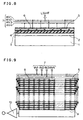
- Fig. 8 is a cross-sectional view of a solid-state image sensor in accordance with a preferred embodiment of the present invention.
- Fig. 9 is a plan view of a full-frame type CCD image sensor in accordance with a preferred embodiment of the present invention.
- Fig. 10 is a plan view of a full-frame type CCD image sensor in accordance with a preferred embodiment of the present invention.
- Fig. 11 is a cross-sectional view illustrating a structure of a contact between a metal wiring layer and an electrode.
- Fig. 8 is a cross-sectional view of a solid-state image sensor in accordance with the first embodiment.
- the illustrated solid-state image sensor is designed to include an n-type silicon substrate 1, a p-type well 2 formed in the n-type silicon substrate 1, and an n-type CCD channel 3 in the vicinity of a surface of the silicon substrate 1 and over the p-type well 2.
- the n-type silicon substrate 1 contains phosphorus at about 10 13 to about 10 15 cm -3
- the p-type well 2 has a depth in the range of 2 ⁇ m to 4 ⁇ m and contains boron at about 10 15 to about 10 16 cm -3
- the n-type CCD channel 3 has a depth in the range of 0.5 ⁇ m to 1 ⁇ m and contains phosphorus or arsenic at about 10 16 to about 10 17 cm -3 .
- a gate dioxide film 4 is formed over the n-type CCD channel 3 by thermal oxidation.
- the gate dioxide film 4 has a thickness in the range of about 20 nm to about 200 nm.
- a plurality of vertical CCD electrodes 5 composed of titanium dioxide (TiO 2 ) is formed on the gate dioxide film 4. The adjacent vertical CCD electrodes 5 are spaced away from each other. As mentioned later, the vertical CCD electrodes 5 are entirely covered with a cover film 6.
- a titanium dioxide (TiO 2 ) film is formed by reactive sputtering in which there are used titanium as a target and sputter gas including a partial pressure of oxygen at 5 to 50%, sputtering in which titanium dioxide (TiO 2 ) is a target, or plasma-enhanced chemical vapor deposition (PCVD) employing titanium tetrachloride (TiCl 4 ) and oxygen.
- the titanium dioxide (TiO 2 ) film has a thickness in the range of 0.1 to 2 ⁇ m.
- a product is annealed at a pressure of 1 ⁇ 10 -5 Torr or smaller, namely, in degree of vacuum in the order of 10 -6 Torr or greater at 300°C to 1200°C, or annealed at 300°C to 1000°C in hydrogen atmosphere, after the titanium dioxide (TiO 2 ) film has been formed.
- hydrogen atmosphere covers from an atmosphere established by a mixture gas of hydrogen at 10 % or greater and a rare gas such as helium and argon to an atmosphere established by 100% of hydrogen. Annealing time is a few minutes to a few hours.
- At least one of tungsten (W), phosphorus (P), antimony (Sb), tantalum (Ta), niobium (Nb), indium (In) and oxides thereof may be doped into a titanium dioxide (TiO 2 ) film for reducing resistivity.
- tungsten, phosphorus, antimony and indium they may be distributed in the vicinity of a surface of the titanium dioxide (TiO 2 ) film by ion-implantation, after the titanium dioxide (TiO 2 ) film has been formed, and doped wholly into the titanium dioxide (TiO 2 ) film by annealing.
- titanium sputtering target or a titanium dioxide (TiO 2 ) sputtering target containing any one of the above listed impurities at 10 19 to 10 21 cm -3 it would be easier to prepare a titanium sputtering target or a titanium dioxide (TiO 2 ) sputtering target containing any one of the above listed impurities at 10 19 to 10 21 cm -3 , and dope the impurities into the titanium dioxide (TiO 2 ) film by sputtering at the same time when the titanium dioxide (TiO 2 ) film is formed.
- the reduction of resistivity may be insufficient by either one of the above-mentioned methods, if a diameter of crystal grain was small, since a surface condition and/or surface morphology before formation of the titanium dioxide (TiO 2 ) film exerts an influence on a diameter of crystal grain.
- an increase in carriers may be facilitated by carrying out both the annealing in vacuum or in hydrogen atmosphere and the impurity doping, to thereby reduce resistivity.
- the titanium dioxide (TiO 2 ) film is patterned into a vertical CCD electrode shape by dry etching.
- impurities are doped into the titanium dioxide (TiO 2 ) film by ion-implantation
- the above-mentioned dry etching has to be carried out after the ion-implantation.
- resistivity is to be reduced by other methods than impurities doping by ion-implantation
- the above-mentioned dry etching may be carried out immediately after the formation of the thin titanium dioxide (TiO 2 ) film.
- An electrode may be a single layer electrode formed by etching a single, thin titanium dioxide (TiO 2 ) film to form spaces between vertical CCD electrodes, as illustrated in Fig. 8.
- an electrode may be a dual layer electrode comprising two thin titanium dioxide (TiO 2 ) films patterned into vertical CCD electrodes, and an interlayer insulating film sandwiched between the two thin titanium dioxide (TiO 2 ) films like a solid-state image sensor reported by D. H. McCann et al..
- titanium dioxide (TiO 2 ) into the vertical CCD electrodes 5 After patterning the titanium dioxide (TiO 2 ) into the vertical CCD electrodes 5, boron ions are implanted into the n-type channel 13 below the spaces between the vertical CCD electrodes 5 at about 10 keV to about 100 keV in dependence on a thickness of the gate dioxide film 4 with doses of 1 ⁇ 10 10 - 1 ⁇ 10 13 cm -2 by using the vertical CCD electrodes 5 as a mask, followed by annealing over the temperature range of about 700°C to about 1000°C for a few minutes to a few hours in vacuum or in hydrogen atmosphere.
- the characteristics of the titanium dioxide (TiO 2 ) vertical CCD electrodes 5 are kept not varied, even when the vertical CCD electrodes 5 are exposed to the atmosphere, if the TiO 2 vertical CCD electrodes 5 have an electrical conductivity by impurities doped thereinto.
- the TiO 2 vertical CCD electrodes 5 have an electrical conductivity by being thermally treated in vacuum or in hydrogen atmosphere, if the impurities are annealed at a higher temperature or in different atmospheres, it is preferable to form an insulating film such as a silicon oxide film or a silicon nitride film before annealing.
- an insulating film can be solidified by being burnt after the formation of the titanium dioxide (TiO 2 ) film, even if a silicon oxide film or a silicon nitride film may be formed by low temperature process as an insulating film, it would be possible to have desired characteristics by burning for solidification. If a silicon oxide film or a silicon nitride film may be formed by high temperature thermal CVD in which film formation temperature is about 800°C, desired characteristics of an insulating film may be obtained without burning the film for solidification.
- an electrode When an electrode is to be formed as a dual layer electrode, a lower layer is first patterned into a vertical CCD electrode shape, and then an interlayer insulating film is formed on the patterned lower layer.
- the above-mentioned silicon dioxide film or silicon nitride film formed by high temperature thermal CVD may be used as the interlayer insulating film. Since the silicon dioxide film or silicon nitride film formed by high temperature thermal CVD has insulating breakdown voltage of about 1 ⁇ 10 7 V/cm, the interlayer insulating film may be reduced in a thickness down to 20 nm, even if an insulating breakdown voltage of 20V is required between lower and upper layer vertical CCD electrodes, for instance.
- the interlayer insulating film doubles as a gate insulating film disposed below the upper layer vertical CCD electrodes. Since CCD would have an enhanced charge transfer ability by reducing a gate insulating film in a thickness, a greater amount of transfer charges might be transferred by reducing a thickness of the interlayer insulating film.
- the upper layer composed of titanium dioxide (TiO 2 ) is patterned into vertical CCD electrodes in the same manner as that of the lower layer vertical CCD electrodes. Thereafter, an insulating film is deposited over the upper layer vertical CCD electrodes in the same manner as that of the single-layered electrode.
- the planarizing film may be composed of PSG or BPSG having a high film-quality and high reliability, which needs a planarizing temperature in the range of about 800°C to about 1000°C.
- contact holes are formed throughout the insulating film, followed by annealing at about 800°C to about 1100°C in nitrogen atmosphere, to thereby smooth a shape of the contact holes and alter a portion of the titanium dioxide (TiO 2 ) vertical CCD electrodes 5 open to the contact hole into titanium nitride (TiN).
- annealing is carried out at about 800°C to about 1100°C in the same atmosphere as a conventional atmosphere in which boron is diffused into silicon employing argon gas as a carrier gas, to thereby smooth a shape of the contact holes and alter a portion of the titanium dioxide (TiO 2 ) vertical CCD electrodes 5 open to the contact hole into titanium boride (TiB 2 ).
- an internal metal wiring layer 50 is formed over the insulating film 51 so that the internal metal wiring layer 50 is contained in the contact hole.
- the internal metal wiring layer 50 is composed of a metal such as aluminum, copper, gold, molybdenum, and tungsten.
- a contact between the internal metal wiring layer 50 and the vertical CCD electrodes 5 has a structure of wiring metal 50/TiN 52/TiO 2 5 or wiring metal 50/TiB 2 53/TiO 2 5.
- titanium nitride (TiN) and titanium boride (TiB 2 ) have resistivity lower by figures than that of the titanium dioxide (TiO 2 ) vertical CCD electrodes 5, specifically, resistivity in the range of 10 -4 ⁇ cm to 10 -5 ⁇ cm and in the range of 10 -5 ⁇ cm to 10 -6 ⁇ cm, respectively, they make a buffer layer forming a preferred ohmic contact with wiring metal, and in addition, they act as barrier metal for preventing abnormal reaction, ensuring desired contact characteristic.
- the contact holes and the internal metal wiring layer are formed in a region not illustrated in Fig. 8.
- Fig. 8 illustrates a relation between the vertical CCDs electrodes 5 and signals 7 for driving them in the case that the vertical CCDs are of four-phase drive.
- a metal light-shield is formed on the insulating film composed of silicon dioxide or silicon nitride in a region not illustrated in Fig. 8 for defining a light-receiving region therewith.
- the metal light-shield is composed of aluminum, copper, gold, molybdenum or tungsten.
- a protection film composed of silicon dioxide, silicon nitride or other materials is formed over the device.
- the cover film 6 covering the vertical CCD electrodes 5 is comprised of the insulating film formed immediately on the titanium dioxide (TiO 2 ) vertical CCD electrodes 5, the film for planarization, the insulating formed on the internal metal wiring layer, and the protection film formed over the device.
- the cover film 6 over the lower layer vertical CCD electrodes includes an interlayer insulating film formed on the lower layer vertical CCD electrodes.
- the cover film 6 is composed entirely of a silicon dioxide film (a PSG film and a BPSG film are one of silicon dioxide films), reflection at a surface of the cover film 6 can be reduced to thereby have high sensitivity by, since an index of refraction of a silicon dioxide film is about 1.45, arranging the cover film 6 to have a total thickness equal to ⁇ /5.8 multiplied by an odd number, wherein ⁇ /5.8 is obtained by introducing the index of refraction, 1.45, into the equation ⁇ /4n.
- ⁇ indicates a wavelength of a light
- n indicates an index of refraction of a film in question.
- an insulating film to be formed on the vertical CCD electrodes 5 composed of titanium dioxide (TiO 2 ) is made of a silicon nitride film, and the film (PSG or BPSG) for planaraization formed in the light-receiving region is removed by etching with the insulating film made of a silicon nitride film used as an etching stopper, it would be possible to compose the entire cover film 6 in the fight-receiving region of a silicon nitride film, in which case, high sensitivity can be obtained by arranging the cover film 6 to have a total thickness equal to ⁇ /8 multiplied by an odd number, wherein ⁇ /8 is obtained by introducing the index of refraction of a silicon nitride film, 2, into the equation ⁇ /4n.
- indexes of refraction of first, second and third layers in the multi-layered structure are represented with N 1 , N 2 and N 3 , respectively.
- the second layer is arranged to have a thickness equal to ⁇ /4N 2 multiplied by an odd number.
- a relation among N 1 , N 2 and N 3 is N 1 ⁇ N 2 , N 2 >N 3 or N 1 >N 2 , N 2 ⁇ N 3
- the second layer is arranged to have a thickness equal to ⁇ /4N 2 multiplied by an even number.
- the titanium dioxide (TiO 2 ) vertical CCD electrodes 5 it would be preferable for the titanium dioxide (TiO 2 ) vertical CCD electrodes 5 to have a thickness equal to ⁇ /4N multiplied by an even number, since titanium dioxide (TiO 2 ) has a greater index of refraction than that of the gate insulating film composed of a silicon dioxide film or a silicon nitride film. It is also preferable for the gate insulating film to have a thickness equal to ⁇ /4N multiplied by an even number. However, if the gate insulating film became thicker to do so, a transfer ability of the vertical CCD would be degraded. Hence, it would be better in some cases to arrange the gate insulating film to have a thickness smaller than ⁇ /4N, considering the reduction in a transfer ability of the vertical CCD, to thereby significantly reduce optical interference effect in the gate insulating film.
- Fig. 9 illustrates a full-frame type CCD image sensor in accordance with the second embodiment.
- a plurality of p + type channel stop regions 8 divides a charge transfer channel into vertical sections to thereby define pixel rows in the number corresponding to the number of horizontal pixels.
- Each one of the channel stop 8 has a depth in the range of 1 ⁇ m to 4 ⁇ m, and has a boron concentration in the range of 10 17 to 10 19 cm -3 .
- a group of vertical CCDs 5 composed of titanium dioxide (TiO 2 ) is arranged perpendicularly to the channel stops 8. Signals 7 for driving the vertical CCDs 5 are transmitted to the CCD transfer electrodes 5 through left and right ends thereof.
- the illustrated full-frame type CCD image sensor does not have a storage section unlike a frame transfer type CCD image sensor, and includes a horizontal CCD 9 connected directly to a light-receiving region composed of the vertical CCDs 5, at a termination end thereof.
- the horizontal CCD 9 receives signal charges at a line at a time from the light-receiving region, and transmits the thus received signal charges to an output section 10 in the form of time sequence signals.
- the output section 10 carries out detection of signal charges and conversion of the detected charges into voltage, and emits the signal voltage as an output.
- the horizontal CCD transfer electrodes and the gate electrodes in a region other than the light-receiving region may be composed of titanium dioxide (TiO 2 ) or polysilicon.
- the signal charges are read out by closing a mechanical shutter when optical signal charges in an image have been finished to accumulate, and then by the same steps as steps for reading out charges out of a storage section in the above-mentioned conventional frame transfer type CCD image sensor.
- Fig. 10 illustrates another full-frame type CCD image sensor in accordance with the third embodiment of the present invention.
- signals 7 for driving the vertical CCDs 5 are transmitted to the vertical CCDs 5 through left and right ends thereof.
- Metal wirings 11 are formed on the channel stops 8.
- Contacts 12 for ensuring electrical connection between the metal wirings and the electrodes 5 are offset by a distance corresponding to one stage of the vertical CCDs 5.
- the vertical CCDs 5 are of four-phase drive, and hence, the contacts 12 are offset every four rows of the electrodes 5.
- the driving signals 7 are also supplied to the vertical CCDs 5 through the metal wirings 11 and the contacts 12.
- a load caused by wiring resistance and vertical CCD resistance is significantly decreased when the driving signals 7 are supplied to the vertical CCDs 5.
- delay and decay of the driving signals 7 are prevented to thereby ensure that the full-frame type CCD image sensor in accordance with the third embodiment has a higher charge transfer ability than the second embodiment illustrated in Fig. 9.
- an electrical conductivity type in each of the regions may be replaced with an opposite electrical conductivity type. Namely, a p-type conductivity may be replaced with an n-type conductivity, and vice versa.
- a dual-layered titanium dioxide CCD electrode is to be applied to CID image sensor, lower and upper layers are arranged perpendicularly to each other.
- the inventor fabricated a four-phase drive, vertical CCD type full-frame CCD image sensor having a structure as illustrated in Fig. 10 and also having effective pixels of 640 (H) ⁇ 480(V).
- an epitaxial silicon substrate comprising an n-type (100) silicon substrate containing phosphorus at about 2 ⁇ 10 14 cm -3 , and a 20 ⁇ m-thick epitaxial silicon layer formed on the n-type (100) silicon substrate and containing phosphorus at the same concentration.
- a p-type well containing boron at about 5 ⁇ 10 15 cm -3 and having a depth of about 3 ⁇ m was formed in the epitaxial silicon substrate.
- n-type CCD channel containing phosphorus at about 5 ⁇ 10 16 cm -3 and having a depth of about 1 ⁇ m was formed in the p-type well.
- the n-type CCD channel was perpendicularly divided into sections by channel stops arranged at a pitch of 10 ⁇ m.
- the channel stops had a depth of about 2 ⁇ m and contained boron at about 8 ⁇ 10 17 cm -3 .
- a gate oxide film was formed over a surface of the n-type CCD channel by a thickness of 50 nm by thermal oxidation.
- the reason why the gate oxide film was designed to have a thickness of 50 nm is as follows. Introduction of 550 nm, which is almost main wavelength in a wavelength band of visible radiation, to the equation 2 ⁇ /4n makes 190 nm, which is relatively thick as a film thickness of a gate oxide film. Hence, the thickness 190 nm may be adopted. However, if a gate oxide film was designed to have a thickness smaller than 95 nm corresponding to ⁇ /4n, it would be possible to enhance an ability of vertical CCD, and reduce interference effect with the result of smaller optical loss.
- TiO 2 titanium dioxide
- the titanium dioxide (TiO 2 ) vertical CCD electrodes were fabricated as follows. First, a titanium dioxide (TiO 2 ) layer was formed by reactive sputtering in which titanium was used as a target and there was employed an argon gas including oxygen at a partial pressure of 30%. The thus formed titanium dioxide (TiO 2 ) layer was annealed at 500°C for three hours in a vacuum kept in the order of 10 -7 Torr, and then dry-etched to thereby form 0.3 ⁇ m-spaces.
- titanium dioxide (TiO 2 ) vertical CCD electrodes were completed as a single layer electrode structure including electrodes having a width of 2.2 ⁇ m.
- a pixel had a dimension of 10 ⁇ m ⁇ in the four-phase drive type vertical CCD.
- the resistivity of the titanium dioxide (TiO 2 ) vertical CCD electrodes was 1 ⁇ 10 -2 to 2 ⁇ 10 -2 ⁇ cm. Resistivity almost the same as the above-mentioned one was obtained also by reactive sputtering in which titanium containing impurities such as phosphorus at about 1 ⁇ 10 20 cm -3 was uses as a target, or by sputtering in which titanium dioxide (TiO 2 ) containing impurities at the same concentration was uses as a target.
- the vertical CCD electrodes were designed to have a thickness of 550 nm, since it had been known by measurement that an index of refraction thereof was 2.5.
- the n-type channel was perpendicularly implanted at 50 keV with doses of 6 ⁇ 10 11 cm -2 boron at the spaces formed between the adjacent vertical CCD electrodes (it should be noted that ion-implantation is usually carried out at an angle of about 7 degrees from a normal line of a substrate).
- a silicon dioxide film was formed by a thickness of 50 nm by high temperature thermal CVD, and BPSG film was further formed on the silicon dioxide film by a thickness of 400 nm, followed by annealing for planarization at 950°C for 30 minutes in steam atmosphere.
- the product was annealed at 950°C for 30 minutes in nitrogen atmosphere to thereby smooth a shape of the contact holes, and further a surface portion of the titanium dioxide vertical CCD electrodes exposed to the contact holes was altered into titanium nitride (TiN).
- an internal metal wiring layer composed of aluminum was formed above the channel stops and around the light-receiving region.
- a silicon dioxide film was formed over the internal metal wiring layer for insulation by a thickness of 400 nm by plasma-enhanced CVD.
- a metal light-shield composed of aluminum was formed for defining the light-receiving region, and an outermost portion of the device was covered with a 200 nm-thick silicon dioxide film by plasma-enhanced CVD.
- the cover film formed on the titanium dioxide (TiO 2 ) vertical CCD electrodes was comprised of a silicon dioxide film having a thickness of 1050 nm which corresponds to about 11 ⁇ /4n wherein a wavelength ⁇ is 550 nm.
- a two-phase drive type horizontal CCD and a transistor of an output section were already formed by ordinary two-layer polysilicon process before the titanium dioxide vertical CCD electrodes had been formed.
- the vertical CCD and the horizontal CCD were connected with each other through dummy pixels below the metal light-shield. Then, a through-hole was formed throughout a silicon dioxide film formed on bonding pads.
- the thus fabricated full-frame type CCD image sensor was operated at 30 frames per second in order to test the performance thereof.
- the image sensor was exposed to a light for about 16.7 milliseconds to thereby accumulate image signals, and then the mechanical shutter was closed for about 16.7 milliseconds to thereby transfer charges and output the image signals. The above-mentioned operation was repeated.
- a frequency of the vertical CCD driving signals was about 30 kHz. The result was that no transfer fault was found. Since the titanium dioxide vertical CCD electrodes between the contacts arranged at a pitch of 40 ⁇ m had a significantly low resistance, specifically, in the range of about 3.3 to about 6.6 k ⁇ , a driving frequency is not limited by a resistance of the titanium dioxide vertical CCD electrodes and electrostatic capacity of a tiny area of the electrodes, but rather limited by a resistance of the internal metal wiring layer composed of aluminum and electrostatic capacity of the light-receiving region having a larger area and connected to the internal metal wiring layer. It was estimated that charge transfer could be carried out at a frequency up to about 20 MHz without any fault. This driving frequency is sufficiently used for high-speed transfer in a frame transfer type CCD image sensor. A quantum efficiency was equal to or greater than 60% over a visible radiation band, and was over 70% at maximum at a frequency of about 550 nm to about 600 nm.
- the solid-state image sensor in accordance with the present invention provides a high quantum efficiency which would be obtained when transparent, electrically conductive material such as ITO (In 2 O 3 -SnO 2 ) and tin oxide (SnO 2 ) is used.
- transparent, electrically conductive material such as ITO (In 2 O 3 -SnO 2 ) and tin oxide (SnO 2 ) is used.
- the solid-state image sensor enhances designability, performance limits and productivity, since it has no limitation in fabrication which would exist when the above-mentioned transparent, electrically conductive material is used.
Abstract
Description
Claims (23)
- A solid-state image sensor comprising a photodetector array in which a plurality of photodetectors are one- or two-dimensionally arranged, each one of the photodetctors including an electrode in a photoelectric conversion region, and transmitting signals when detecting a light passing through the electrode (5), the solid-state image sensor converting the signals into time sequence electric signals, characterized by that
the electrode (5) being composed of titanium dioxide (TiO2). - The solid-state image sensor as set forth in claim 1, wherein the titanium dioxide contains oxygen vacancies.
- The solid-state image sensor as set forth in claim 1, wherein the titanium dioxide contains at least one of tungsten (W), phosphorus (P), antimony (Sb), tantalum (Ta), niobium (Nb), indium (In) and oxides thereof (WO3, P2O5, Sb2O5, Ta2O5, Nb2O5, In2O3).
- The solid-state image sensor as set forth in claim 2, wherein the titanium dioxide contains at least one of tungsten (W), phosphorus (P), antimony (Sb), tantalum (Ta), niobium (Nb), indium (In) and oxides thereof (WO3, P2O5, Sb2O5, Ta2O5, Nb2O5, In2O3).
- The solid-state image sensor as set forth in claim 3 or 4, wherein a doping concentration is in the range of 1 × 1019 cm-3 to 1 × 1021 cm-3.
- The solid-state image sensor as set forth in any one of claims 1 to 4, wherein the titanium dioxide contains anatase phase.
- The solid-state image sensor as set forth in any one of claims 1 to 4, wherein the titanium dioxide is in the form of a film having a thickness in the range of 0.1 µm to 2 µm both inclusive.
- The solid-state image sensor as set forth in any one of claims 1 to 4, wherein the titanium dioxide makes electrical contact through a titanium nitride film with wiring metal contained in a contact hole formed throughout an insulating layer formed on the titanium dioxide, thus a contact structure of (wiring metal)/TiN/TiO2 being established.
- The solid-state image sensor as set forth in any one of claims 1 to 4, wherein the titanium dioxide makes electrical contact through a titanium boride film with wiring metal contained in a contact hole formed throughout an insulating layer formed on the titanium dioxide, thus a contact structure of (wiring metal)/TiB2/TiO2 being established.
- The solid-state image sensor as set forth in any one of claims 1 to 4, wherein the titanium dioxide is in the form of a single layer, which is formed with a plurality of spaces to thereby define electrodes (5) therebetween.
- The solid-state image sensor as set forth in any one of claims 1 to 4, wherein the titanium dioxide is in the form of upper and lower layers (35, 37), the lower layer being formed with a plurality of spaces to thereby define first electrodes (35) therebetween, the first electrodes (35) being covered with an insulating film (36), the upper layer (37) being formed on the spaces of the lower layer.
- The solid-state image sensor as set forth in claim 11, wherein a channel below the spaces are doped with impurities having a conductivity type opposite to that of the channel.
- The solid-state image sensor as set forth in any one of claims 1 to 4, further comprising an insulating film composed of PSG or BPSG and covering the titanium dioxide therewith.
- A method of fabricating a solid-state image sensor, comprising the steps of:(a) forming a titanium dioxide (TiO2) film as an electrode in a photoelectric conversion region; and(b) annealing the titanium dioxide film in vacuum at a pressure of 1 × 10⁻⁵ Torr or smaller at 300°C to 1200°C both inclusive.
- The method as set forth in claim 14, further comprising the steps of:(c) forming an insulating film over the titanium dioxide film;(d) forming a contact hole throughout the insulating film; and(e) annealing the product of the step (d) at 800°C to 1100°C in nitrogen atmosphere for altering a portion of the titanium dioxide film exposed to the contact hole into titanium nitride (TiN).
- The method as set forth in claim 14, further comprising the steps of:(c) forming an insulating film over the titanium dioxide film;(d) forming a contact hole throughout the insulating film; and(e) annealing the product of the step (d) at 800°C to 1100°C in boron atmosphere for altering a portion of the titanium dioxide film exposed to the contact hole into titanium boride (TiB2).
- A method of fabricating a solid-state image sensor, comprising the steps of:(a) forming a titanium dioxide (TiO2) film as an electrode in a photoelectric conversion region; and(b)annealing the titanium dioxide film at 300°C to 1000°C both inclusive in an atmosphere containing hydrogen at 10 % to 100 % both inclusive.
- The method as set forth in claim 17, further comprising the steps of:(c) forming an insulating film over the titanium dioxide film;(d) forming a contact hole throughout the insulating film; and(e) annealing the product of the step (d) at 800°C to 1100°C in nitrogen atmosphere for altering a portion of the titanium dioxide film exposed to the contact hole into titanium nitride (TiN).
- The method as set forth in claim 17, further comprising the steps of:(c) forming an insulating film over the titanium dioxide film;(d) forming a contact hole throughout the insulating film; and(e) annealing the product of the step (d) at 800°C to 1100°C in boron atmosphere for altering a portion of the titanium dioxide film exposed to the contact hole into titanium boride (TiB2).
- A method of fabricating a solid-state image sensor, comprising the step of forming a titanium dioxide (TiO2) film as an electrode in a photoelectric conversion region by sputtering, employing titanium or titanium dioxide as a target containing at least one of tungsten (W), phosphorus (P), antimony (Sb), tantalum (Ta), niobium (Nb), indium (In) and oxides thereof (WO3, P2O5, Sb2O5, Ta2O5, Nb2O5, In2O3).
- The method as set forth in claim 20, wherein the titanium or titanium dioxide as a target contains at least one of tungsten (W), phosphorus (P), antimony (Sb), tantalum (Ta), niobium (Nb), indium (In) and oxides thereof (WO3, P2O5, Sb2O5, Ta2O5, Nb2O5, In2O3) at a concentration in the range of 1019 to 1021 cm-3.
- The method as set forth in claim 20, further comprising the steps of:(c) forming an insulating film over the titanium dioxide film;(d) forming a contact hole throughout the insulating film; and(e) annealing the product of the step (d) at 800°C to 1100°C in nitrogen atmosphere for altering a portion of the titanium dioxide film exposed to the contact hole into titanium nitride (TiN).
- The method as set forth in claim 20, further comprising the steps of:(c) forming an insulating film over the titanium dioxide film;(d) forming a contact hole throughout the insulating film; and(e) annealing the product of the step (d) at 800°C to 1100°C in boron atmosphere for altering a portion of the titanium dioxide film exposed to the contact hole into titanium boride (TiB2).
Applications Claiming Priority (2)
| Application Number | Priority Date | Filing Date | Title |
|---|---|---|---|
| JP24956/97 | 1997-02-07 | ||
| JP9024956A JP3019797B2 (en) | 1997-02-07 | 1997-02-07 | Solid-state imaging device and method of manufacturing the same |
Publications (2)
| Publication Number | Publication Date |
|---|---|
| EP0858112A2 true EP0858112A2 (en) | 1998-08-12 |
| EP0858112A3 EP0858112A3 (en) | 1999-01-20 |
Family
ID=12152448
Family Applications (1)
| Application Number | Title | Priority Date | Filing Date |
|---|---|---|---|
| EP98101889A Withdrawn EP0858112A3 (en) | 1997-02-07 | 1998-02-04 | Solid-state image sensor and method of fabricating the same |
Country Status (3)
| Country | Link |
|---|---|
| US (1) | US6018169A (en) |
| EP (1) | EP0858112A3 (en) |
| JP (1) | JP3019797B2 (en) |
Cited By (5)
| Publication number | Priority date | Publication date | Assignee | Title |
|---|---|---|---|---|
| WO2000026967A1 (en) * | 1998-11-02 | 2000-05-11 | Hamamatsu Photonics K.K. | Semiconductor energy sensor |
| EP1796107A1 (en) * | 2004-08-13 | 2007-06-13 | Kanagawa Academy of Science and Technology | Transparent conductor, transparent electrode, solar cell, luminescent device and display panel |
| WO2012015632A1 (en) * | 2010-07-29 | 2012-02-02 | Image Sensor Technologies Acquisition Corporation | Ccd sensors with multiple contact patterns |
| WO2012015627A1 (en) * | 2010-07-29 | 2012-02-02 | Eastman Kodak Company | Ccd sensors with multiple contact patterns |
| US8293663B2 (en) | 2010-07-29 | 2012-10-23 | Truesense Imaging, Inc. | CCD sensors with multiple contact patterns |
Families Citing this family (18)
| Publication number | Priority date | Publication date | Assignee | Title |
|---|---|---|---|---|
| JP3988239B2 (en) | 1998-03-19 | 2007-10-10 | ソニー株式会社 | Solid-state imaging device and manufacturing method thereof |
| JP4493124B2 (en) * | 1999-08-04 | 2010-06-30 | 日本テキサス・インスツルメンツ株式会社 | Solid-state imaging device |
| DE10140514A1 (en) | 2001-08-17 | 2003-02-27 | Heraeus Gmbh W C | Sputtering target based on titanium dioxide |
| FR2838561B1 (en) * | 2002-04-12 | 2004-09-17 | Commissariat Energie Atomique | PHOTODECTOR MATRIX, PIXEL ISOLATED BY WALLS, HYBRIDED ON A READING CIRCUIT |
| US7430897B2 (en) * | 2002-09-19 | 2008-10-07 | National Research Council Of Canada | Method and apparatus for detecting and locating gas leaks |
| JP2004140258A (en) * | 2002-10-18 | 2004-05-13 | Sanyo Electric Co Ltd | Solid-state imaging device and manufacture thereof |
| ATE474071T1 (en) * | 2003-08-11 | 2010-07-15 | Honeywell Int Inc | TARGET/SUPPORT PLATE CONSTRUCTIONS AND MANUFACTURING METHODS THEREOF |
| JP4496751B2 (en) * | 2003-10-09 | 2010-07-07 | 日本電気株式会社 | Thermal infrared solid-state imaging device and manufacturing method thereof |
| JP2006049451A (en) * | 2004-08-03 | 2006-02-16 | Sony Corp | Solid state image pickup device and driving method thereof |
| WO2006073189A1 (en) * | 2005-01-08 | 2006-07-13 | Kanagawa Academy Of Science And Technology | Functional device and method for forming oxide material |
| JP2007053183A (en) * | 2005-08-17 | 2007-03-01 | Fujifilm Corp | Solid-state imaging device |
| WO2007120176A2 (en) * | 2005-09-09 | 2007-10-25 | University Of Nevada, Reno | Preparation of nano-tubular titania substrate with oxygen vacancies and their use in photo-electrolysis of water |
| US7524690B2 (en) * | 2006-08-10 | 2009-04-28 | United Microelectronics Corp. | Image sensor with a waveguide tube and a related fabrication method |
| CN100413084C (en) * | 2006-09-18 | 2008-08-20 | 西安理工大学 | Circuitous transition surface array charge-coupled device |
| US20110073982A1 (en) * | 2007-05-25 | 2011-03-31 | Armstrong J Joseph | Inspection system using back side illuminated linear sensor |
| JP2011009502A (en) * | 2009-06-26 | 2011-01-13 | Showa Denko Kk | Light emitting element and method of manufacturing the same, lamp, electronic apparatus, and mechanical apparatus |
| FR2971084B1 (en) * | 2011-01-28 | 2013-08-23 | E2V Semiconductors | MULTILINEAR IMAGE SENSOR WITH CHARGE INTEGRATION |
| US8987788B2 (en) | 2011-09-26 | 2015-03-24 | Semiconductor Components Industries, Llc | Metal-strapped CCD image sensors |
Citations (4)
| Publication number | Priority date | Publication date | Assignee | Title |
|---|---|---|---|---|
| US4012767A (en) * | 1976-02-25 | 1977-03-15 | General Electric Company | Electrical interconnections for semi-conductor devices |
| JPH02229473A (en) * | 1989-03-01 | 1990-09-12 | Ricoh Co Ltd | Manufacture of patterned photoconductor element |
| US4994405A (en) * | 1989-11-21 | 1991-02-19 | Eastman Kodak Company | Area image sensor with transparent electrodes |
| US5565676A (en) * | 1993-12-27 | 1996-10-15 | Nec Corporation | Method of driving photoelectric conversion device |
Family Cites Families (3)
| Publication number | Priority date | Publication date | Assignee | Title |
|---|---|---|---|---|
| JPS5941351B2 (en) * | 1976-09-13 | 1984-10-06 | 株式会社日立製作所 | Color solid-state image sensor |
| US4720746A (en) * | 1985-08-05 | 1988-01-19 | Eastman Kodak Company | Frame transfer CCD area image sensor with improved horizontal resolution |
| JPH0685583B2 (en) * | 1986-05-27 | 1994-10-26 | 富士写真フイルム株式会社 | Solid-state image sensor for color |
-
1997
- 1997-02-07 JP JP9024956A patent/JP3019797B2/en not_active Expired - Fee Related
-
1998
- 1998-02-04 EP EP98101889A patent/EP0858112A3/en not_active Withdrawn
- 1998-02-05 US US09/019,470 patent/US6018169A/en not_active Expired - Lifetime
Patent Citations (4)
| Publication number | Priority date | Publication date | Assignee | Title |
|---|---|---|---|---|
| US4012767A (en) * | 1976-02-25 | 1977-03-15 | General Electric Company | Electrical interconnections for semi-conductor devices |
| JPH02229473A (en) * | 1989-03-01 | 1990-09-12 | Ricoh Co Ltd | Manufacture of patterned photoconductor element |
| US4994405A (en) * | 1989-11-21 | 1991-02-19 | Eastman Kodak Company | Area image sensor with transparent electrodes |
| US5565676A (en) * | 1993-12-27 | 1996-10-15 | Nec Corporation | Method of driving photoelectric conversion device |
Non-Patent Citations (3)
| Title |
|---|
| GRANT F.A.: "Properties of Rutile (Titanium Dioxide)" REVIEWS OF MODERN PHYSICS, vol. 31, no. 3, June 1959, pages 646-674, XP002084852 * |
| PATENT ABSTRACTS OF JAPAN vol. 014, no. 541 (E-1007), 29 November 1990 & JP 02 229473 A (RICOH CO LTD), 12 September 1990 * |
| TANG H ET AL: "Electrical and optical properties of TiO/sub 2/ anatase thin films" JOURNAL OF APPLIED PHYSICS, 15 FEB. 1994, USA, vol. 75, no. 4, pages 2042-2047, XP002084851 ISSN 0021-8979 * |
Cited By (9)
| Publication number | Priority date | Publication date | Assignee | Title |
|---|---|---|---|---|
| WO2000026967A1 (en) * | 1998-11-02 | 2000-05-11 | Hamamatsu Photonics K.K. | Semiconductor energy sensor |
| US6541753B2 (en) | 1998-11-02 | 2003-04-01 | Hammatsu Photonics K.K. | Semiconductor energy detector having reinforcement |
| EP1796107A1 (en) * | 2004-08-13 | 2007-06-13 | Kanagawa Academy of Science and Technology | Transparent conductor, transparent electrode, solar cell, luminescent device and display panel |
| EP1796107A4 (en) * | 2004-08-13 | 2011-10-26 | Kanagawa Kagaku Gijutsu Akad | Transparent conductor, transparent electrode, solar cell, luminescent device and display panel |
| TWI382004B (en) * | 2004-08-13 | 2013-01-11 | Kanagawa Kagaku Gijutsu Akad | Transparent conductor, transparent electrode, solar cell, light emitting element and display panel |
| WO2012015632A1 (en) * | 2010-07-29 | 2012-02-02 | Image Sensor Technologies Acquisition Corporation | Ccd sensors with multiple contact patterns |
| WO2012015627A1 (en) * | 2010-07-29 | 2012-02-02 | Eastman Kodak Company | Ccd sensors with multiple contact patterns |
| US8274100B2 (en) | 2010-07-29 | 2012-09-25 | Truesense Imaging, Inc. | CCD sensors with multiple contact patterns |
| US8293663B2 (en) | 2010-07-29 | 2012-10-23 | Truesense Imaging, Inc. | CCD sensors with multiple contact patterns |
Also Published As
| Publication number | Publication date |
|---|---|
| US6018169A (en) | 2000-01-25 |
| EP0858112A3 (en) | 1999-01-20 |
| JPH10223877A (en) | 1998-08-21 |
| JP3019797B2 (en) | 2000-03-13 |
Similar Documents
| Publication | Publication Date | Title |
|---|---|---|
| US6018169A (en) | Solid-state image sensor and method of fabricating the same | |
| US5235198A (en) | Non-interlaced interline transfer CCD image sensing device with simplified electrode structure for each pixel | |
| US7585695B2 (en) | Lightshield architecture for interline transfer image sensors | |
| US7858433B2 (en) | Photoelectric converting film stack type solid-state image pickup device, and method of producing the same | |
| US6501065B1 (en) | Image sensor using a thin film photodiode above active CMOS circuitry | |
| US7105867B2 (en) | Solid-state imaging device and manufacturing method thereof | |
| KR0175175B1 (en) | Solid state imaging device | |
| EP0409970B1 (en) | Interline transfer ccd image sensing device with electrode structure for each pixel | |
| US6525356B1 (en) | Solid imaging device | |
| US5895944A (en) | Charge coupled device image sensor and method of driving the same | |
| US20110031573A1 (en) | Solid-state imaging device, imaging apparatus, and manufacturing method of solid-state imaging device | |
| EP0428050B1 (en) | Photosensor having an amorphous silicon photoabsorption layer | |
| JP3394308B2 (en) | Solid-state imaging device | |
| US20220238575A1 (en) | Dummy vertical transistor structure to reduce cross talk in pixel sensor | |
| US5142346A (en) | Floating gate JFET image sensor | |
| US6441853B1 (en) | Solid-state image sensor having vertical transfer electrodes protected from short circuiting | |
| JPH04373174A (en) | Solid state image sensing device | |
| JPH0888344A (en) | Solid-state image sensing device | |
| US20240145514A1 (en) | Image sensor | |
| JP3890381B2 (en) | Solid-state imaging device | |
| JP3239934B2 (en) | Solid-state imaging device and method of manufacturing the same | |
| JP2002110959A (en) | Solid-state imaging device and its manufacturing method | |
| WO1991008590A1 (en) | Non-interlaced interline transfer ccd image sensing device with simplified electrode structure for each pixel | |
| JP2001168314A (en) | Solid-state image pick-up device and its manufacturing method | |
| JPH07120781B2 (en) | Solid-state imaging device |
Legal Events
| Date | Code | Title | Description |
|---|---|---|---|
| PUAI | Public reference made under article 153(3) epc to a published international application that has entered the european phase |
Free format text: ORIGINAL CODE: 0009012 |
|
| AK | Designated contracting states |
Kind code of ref document: A2 Designated state(s): DE FR GB NL |
|
| AX | Request for extension of the european patent |
Free format text: AL;LT;LV;MK;RO;SI |
|
| PUAL | Search report despatched |
Free format text: ORIGINAL CODE: 0009013 |
|
| AK | Designated contracting states |
Kind code of ref document: A3 Designated state(s): AT BE CH DE DK ES FI FR GB GR IE IT LI LU MC NL PT SE |
|
| AX | Request for extension of the european patent |
Free format text: AL;LT;LV;MK;RO;SI |
|
| 17P | Request for examination filed |
Effective date: 19990301 |
|
| AKX | Designation fees paid |
Free format text: DE FR GB NL |
|
| 17Q | First examination report despatched |
Effective date: 20021002 |
|
| GRAP | Despatch of communication of intention to grant a patent |
Free format text: ORIGINAL CODE: EPIDOSNIGR1 |
|
| STAA | Information on the status of an ep patent application or granted ep patent |
Free format text: STATUS: THE APPLICATION IS DEEMED TO BE WITHDRAWN |
|
| 18D | Application deemed to be withdrawn |
Effective date: 20050920 |