EP1793656A2 - Flexible printed wiring board - Google Patents
Flexible printed wiring board Download PDFInfo
- Publication number
- EP1793656A2 EP1793656A2 EP05785562A EP05785562A EP1793656A2 EP 1793656 A2 EP1793656 A2 EP 1793656A2 EP 05785562 A EP05785562 A EP 05785562A EP 05785562 A EP05785562 A EP 05785562A EP 1793656 A2 EP1793656 A2 EP 1793656A2
- Authority
- EP
- European Patent Office
- Prior art keywords
- flexible printed
- printed wiring
- wiring board
- conductor
- layer
- Prior art date
- Legal status (The legal status is an assumption and is not a legal conclusion. Google has not performed a legal analysis and makes no representation as to the accuracy of the status listed.)
- Granted
Links
Images






Classifications
-
- H—ELECTRICITY
- H05—ELECTRIC TECHNIQUES NOT OTHERWISE PROVIDED FOR
- H05K—PRINTED CIRCUITS; CASINGS OR CONSTRUCTIONAL DETAILS OF ELECTRIC APPARATUS; MANUFACTURE OF ASSEMBLAGES OF ELECTRICAL COMPONENTS
- H05K1/00—Printed circuits
- H05K1/02—Details
- H05K1/0277—Bendability or stretchability details
- H05K1/028—Bending or folding regions of flexible printed circuits
-
- H—ELECTRICITY
- H01—ELECTRIC ELEMENTS
- H01R—ELECTRICALLY-CONDUCTIVE CONNECTIONS; STRUCTURAL ASSOCIATIONS OF A PLURALITY OF MUTUALLY-INSULATED ELECTRICAL CONNECTING ELEMENTS; COUPLING DEVICES; CURRENT COLLECTORS
- H01R12/00—Structural associations of a plurality of mutually-insulated electrical connecting elements, specially adapted for printed circuits, e.g. printed circuit boards [PCB], flat or ribbon cables, or like generally planar structures, e.g. terminal strips, terminal blocks; Coupling devices specially adapted for printed circuits, flat or ribbon cables, or like generally planar structures; Terminals specially adapted for contact with, or insertion into, printed circuits, flat or ribbon cables, or like generally planar structures
- H01R12/70—Coupling devices
- H01R12/71—Coupling devices for rigid printing circuits or like structures
- H01R12/712—Coupling devices for rigid printing circuits or like structures co-operating with the surface of the printed circuit or with a coupling device exclusively provided on the surface of the printed circuit
- H01R12/714—Coupling devices for rigid printing circuits or like structures co-operating with the surface of the printed circuit or with a coupling device exclusively provided on the surface of the printed circuit with contacts abutting directly the printed circuit; Button contacts therefore provided on the printed circuit
-
- H—ELECTRICITY
- H05—ELECTRIC TECHNIQUES NOT OTHERWISE PROVIDED FOR
- H05K—PRINTED CIRCUITS; CASINGS OR CONSTRUCTIONAL DETAILS OF ELECTRIC APPARATUS; MANUFACTURE OF ASSEMBLAGES OF ELECTRICAL COMPONENTS
- H05K1/00—Printed circuits
- H05K1/02—Details
- H05K1/03—Use of materials for the substrate
- H05K1/0313—Organic insulating material
- H05K1/0353—Organic insulating material consisting of two or more materials, e.g. two or more polymers, polymer + filler, + reinforcement
- H05K1/0366—Organic insulating material consisting of two or more materials, e.g. two or more polymers, polymer + filler, + reinforcement reinforced, e.g. by fibres, fabrics
-
- H—ELECTRICITY
- H05—ELECTRIC TECHNIQUES NOT OTHERWISE PROVIDED FOR
- H05K—PRINTED CIRCUITS; CASINGS OR CONSTRUCTIONAL DETAILS OF ELECTRIC APPARATUS; MANUFACTURE OF ASSEMBLAGES OF ELECTRICAL COMPONENTS
- H05K3/00—Apparatus or processes for manufacturing printed circuits
- H05K3/46—Manufacturing multilayer circuits
- H05K3/4644—Manufacturing multilayer circuits by building the multilayer layer by layer, i.e. build-up multilayer circuits
- H05K3/4682—Manufacture of core-less build-up multilayer circuits on a temporary carrier or on a metal foil
-
- H—ELECTRICITY
- H05—ELECTRIC TECHNIQUES NOT OTHERWISE PROVIDED FOR
- H05K—PRINTED CIRCUITS; CASINGS OR CONSTRUCTIONAL DETAILS OF ELECTRIC APPARATUS; MANUFACTURE OF ASSEMBLAGES OF ELECTRICAL COMPONENTS
- H05K1/00—Printed circuits
- H05K1/02—Details
- H05K1/14—Structural association of two or more printed circuits
- H05K1/141—One or more single auxiliary printed circuits mounted on a main printed circuit, e.g. modules, adapters
-
- H—ELECTRICITY
- H05—ELECTRIC TECHNIQUES NOT OTHERWISE PROVIDED FOR
- H05K—PRINTED CIRCUITS; CASINGS OR CONSTRUCTIONAL DETAILS OF ELECTRIC APPARATUS; MANUFACTURE OF ASSEMBLAGES OF ELECTRICAL COMPONENTS
- H05K2201/00—Indexing scheme relating to printed circuits covered by H05K1/00
- H05K2201/02—Fillers; Particles; Fibers; Reinforcement materials
- H05K2201/0275—Fibers and reinforcement materials
- H05K2201/029—Woven fibrous reinforcement or textile
-
- H—ELECTRICITY
- H05—ELECTRIC TECHNIQUES NOT OTHERWISE PROVIDED FOR
- H05K—PRINTED CIRCUITS; CASINGS OR CONSTRUCTIONAL DETAILS OF ELECTRIC APPARATUS; MANUFACTURE OF ASSEMBLAGES OF ELECTRICAL COMPONENTS
- H05K2203/00—Indexing scheme relating to apparatus or processes for manufacturing printed circuits covered by H05K3/00
- H05K2203/15—Position of the PCB during processing
- H05K2203/1536—Temporarily stacked PCBs
-
- H—ELECTRICITY
- H05—ELECTRIC TECHNIQUES NOT OTHERWISE PROVIDED FOR
- H05K—PRINTED CIRCUITS; CASINGS OR CONSTRUCTIONAL DETAILS OF ELECTRIC APPARATUS; MANUFACTURE OF ASSEMBLAGES OF ELECTRICAL COMPONENTS
- H05K3/00—Apparatus or processes for manufacturing printed circuits
- H05K3/22—Secondary treatment of printed circuits
- H05K3/28—Applying non-metallic protective coatings
-
- H—ELECTRICITY
- H05—ELECTRIC TECHNIQUES NOT OTHERWISE PROVIDED FOR
- H05K—PRINTED CIRCUITS; CASINGS OR CONSTRUCTIONAL DETAILS OF ELECTRIC APPARATUS; MANUFACTURE OF ASSEMBLAGES OF ELECTRICAL COMPONENTS
- H05K3/00—Apparatus or processes for manufacturing printed circuits
- H05K3/36—Assembling printed circuits with other printed circuits
- H05K3/361—Assembling flexible printed circuits with other printed circuits
- H05K3/363—Assembling flexible printed circuits with other printed circuits by soldering
-
- H—ELECTRICITY
- H05—ELECTRIC TECHNIQUES NOT OTHERWISE PROVIDED FOR
- H05K—PRINTED CIRCUITS; CASINGS OR CONSTRUCTIONAL DETAILS OF ELECTRIC APPARATUS; MANUFACTURE OF ASSEMBLAGES OF ELECTRICAL COMPONENTS
- H05K3/00—Apparatus or processes for manufacturing printed circuits
- H05K3/46—Manufacturing multilayer circuits
- H05K3/4644—Manufacturing multilayer circuits by building the multilayer layer by layer, i.e. build-up multilayer circuits
- H05K3/4652—Adding a circuit layer by laminating a metal foil or a preformed metal foil pattern
-
- H—ELECTRICITY
- H10—SEMICONDUCTOR DEVICES; ELECTRIC SOLID-STATE DEVICES NOT OTHERWISE PROVIDED FOR
- H10W—GENERIC PACKAGES, INTERCONNECTIONS, CONNECTORS OR OTHER CONSTRUCTIONAL DETAILS OF DEVICES COVERED BY CLASS H10
- H10W72/00—Interconnections or connectors in packages
- H10W72/851—Dispositions of multiple connectors or interconnections
- H10W72/874—On different surfaces
- H10W72/877—Bump connectors and die-attach connectors
-
- H—ELECTRICITY
- H10—SEMICONDUCTOR DEVICES; ELECTRIC SOLID-STATE DEVICES NOT OTHERWISE PROVIDED FOR
- H10W—GENERIC PACKAGES, INTERCONNECTIONS, CONNECTORS OR OTHER CONSTRUCTIONAL DETAILS OF DEVICES COVERED BY CLASS H10
- H10W90/00—Package configurations
- H10W90/701—Package configurations characterised by the relative positions of pads or connectors relative to package parts
- H10W90/721—Package configurations characterised by the relative positions of pads or connectors relative to package parts of bump connectors
- H10W90/724—Package configurations characterised by the relative positions of pads or connectors relative to package parts of bump connectors between a chip and a stacked insulating package substrate, interposer or RDL
-
- H—ELECTRICITY
- H10—SEMICONDUCTOR DEVICES; ELECTRIC SOLID-STATE DEVICES NOT OTHERWISE PROVIDED FOR
- H10W—GENERIC PACKAGES, INTERCONNECTIONS, CONNECTORS OR OTHER CONSTRUCTIONAL DETAILS OF DEVICES COVERED BY CLASS H10
- H10W90/00—Package configurations
- H10W90/701—Package configurations characterised by the relative positions of pads or connectors relative to package parts
- H10W90/731—Package configurations characterised by the relative positions of pads or connectors relative to package parts of die-attach connectors
- H10W90/734—Package configurations characterised by the relative positions of pads or connectors relative to package parts of die-attach connectors between a chip and a stacked insulating package substrate, interposer or RDL
Definitions
- This invention relates to a flexible printed wiring board, and more particularly, to a flexible printed wiring board having an element mounting part where circuit elements are mounted and a bending part to be bent around a bending axis.
- Such a flexible printed wiring board with CSPs mounted on both surfaces is arranged to have a layered structure throughout the substrate surface, as shown in Fig. 15, typically consisting of three conductor layers (PT 1 to PT3), two insulating layers (1N and IN2) isolating these conductor layers, and two coverlay layers (CL1 and CL2) (hereafter referred to as "related art example").
- memory elements for example, are mounted on both surfaces of an element mounting part 60' as shown in Fig. 15.
- a bending part 70' is bent around the bending axis AX', so that a motherboard connecting part 80', which is formed at the top surface on the other end, is made in electric contact with the motherboard MB (Fig. 15). Consequently, the efficiency in implementation of memory elements on a motherboard can be improved.
- An object of the present invention is to provide a flexible printed wiring board that has improved crack resistance.
- a flexible printed wiring board comprises an element mounting part where circuit elements are mounted and a bending part to be bent around the bending axis.
- An inner conductor layer is formed on the inside of the board.
- element mounting part conductor layers are formed on both surfaces at outer sides of the wiring board, respectively, and in the bending part, a bending part conductor layer is formed only on the surface on the outer side that faces the exterior when the wiring board is bent.
- the element mounting part conductor layers are formed on both surfaces at the outer sides of the wiring board, respectively.
- the bending part conductor layer is formed only on the side that faces the exterior when it is bent. Therefore, as compared with the related art example described above, this configuration allows a reduction of the number of conductor layers in the bending part by one and the number of coverlay layer by one as well.
- the total thickness can be made thin as compared with the related art flexible printed wiring boards. Consequently, when the flexible wiring board is bent at the same curvature, the stress is reduced, and therefore crack resistance is improved.
- a conductor pattern that imparts a ground potential in terms of alternating current may be formed.
- a conductor pattern to impart a ground potential in terms of alternating current as an interior layer conductor layer, the characteristic impedance of a signal circuit pattern (also referred to as "outer layer conductor pattern") formed at the side that faces the exterior can be stabilized even when the flexible printed wiring board is bent along the bending axis.
- a conductor pattern to impart the ground potential in terms of alternating current may be formed in a plane pattern.
- signal lines of the outer layer conductor pattern in the bending part can be formed to constitute a microstrip configuration, thereby further stabilizing the characteristic impedance.
- the insulating layer formed between the above described conductor patterns are preferably made of fiber-reinforced plastic.
- fiber-reinforced plastics there are mentioned fiber-glass reinforced plastics (GFRP), carbon fiber reinforced plastics (CFRP) and the like. More specifically, glass-fiber-reinforced epoxy, glass-fiber-reinforced polyester resin and the like may be used.
- the thickness of the above described insulating layer is preferably between about 25 ⁇ m and about 65 ⁇ m. In this case, when the thickness of the above described insulating layer is less than about 25 ⁇ m, it is difficult to form an insulating layer with a uniform thickness, while when the thickness exceeds about 65 ⁇ m, preferable crack resistance may not be obtained.
- the warp and the weft contained in the above described fiber-reinforced plastic preferably extend in the directions intersecting the direction of the above described bending axis by an angle of about 30° or more and about 60° or less. With this configuration, when the wiring board is bent, the warp and the weft mechanically cooperate to improve crack resistance.
- the signal conductive pattern formed in the above described bending part conductor layer preferably extends in the direction that is obliquely disposed relative to the direction of the above described bending axis. This way, when the bending part is bent around the bending axis, the crack-prevention performance of the signal conductor pattern is further improved and the occurrence of cracks can be further reduced.
- the above described circuit element can be a memory element.
- high density implementation of memory elements which has been desired more and more in recent years, becomes possible.
- one advantage of the present invention is that a flexible printed wiring board with improved crack resistance can be provided.
- Fig. 1 shows a configuration of a flexible printed wiring board 10 according to an embodiment of the present invention as a perspective view.
- Fig.1(A) is a perspective view thereof.
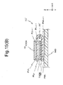
- Fig. 1(B) is an XZ side view of the flexible printed wiring board 10 which is bent at a bending part along the bending axis AX and is attached to a motherboard MB.
- pads 44U 1 to 44U N for mounting a circuit element 100A and pads 47L 1 to 47L N are provided, and pads 44U 1 to 44U N and pads 47L 1 to 47L N are electrically connected, respectively, for example.
- pads 45U 1 to 45U N for mounting a circuit element 100B are formed at locations that correspond to the pads 44U 1 to 44U N .
- these pads 45U 1 to 45U N and pads 47L 1 to 47L N are also electrically connected, respectively.
- circuit element 100A and circuit element 100B can be memory elements of the same type.
- the element 100A is mounted on the upper surface and the element 1008 is mounted on the lower surface of the flexible printed wiring board 10.
- the flexible printed wiring board 10 In mounting the flexible printed wiring board 10 on a host board, such as a mother board, the flexible printed wiring board 10 is bent around the bending axis AX, and is mounted on the motherboard MB, as shown in Fig. 1(B).
- the circuit element 100B of the flexible printed wiring board 10 is bonded via a bonding layer 90 to a surface of the folded-over portion of the flexible printed wiring board, which is opposite to the surface having the pads 47L 1 to 47L N .
- Fig. 2 shows an XZ cross-sectional view of the flexible printed wiring board 10 of the present embodiment.
- the flexible printed wiring board 10 of the present embodiment includes an element mounting parts 60A and 60B (also referred to as "element mounting part 60" collectively) where the circuit elements 100A and 100B as described above are to be mounted, a bending part 70 where this flexible printed wiring board is bent around the bending axis AX, and a motherboard connecting part 80, which is to be connected to a motherboard.
- the flexible printed wiring board 10 includes, in the element mounting part 60, (a) an insulating layer 13, (b) an insulating layer 17U formed on a surface in the +Z direction side of the insulating layer 13, (c) an insulating layer 20U, which is the outmost layer formed on a surface in the +Z direction side of the insulating layer 17U and (d) an insulating layer 22 formed on a surface in the -Z direction side of the insulating layer 13.
- the insulating layers 20U and 22 respectively function as coverlay layers. Since the insulating layer 22 is not formed in the bending part 70, the bending part 70 includes the layers (a) to (c), but does not include the insulating layer 22 (d).
- the flexible printed wiring board 10 includes (c) a conductor pattern 34U' formed on the surface in the +Z direction of the insulating layer 13, (d) a first conductor pattern 36U', which is a signal line pattern, formed on the surface in the +Z direction of the insulating layer 17U and (e) a second conductor pattern 33L, which is a signal line pattern, formed on the surface in the -Z direction of the insulating layer 13 in the element mounting part 60.
- this conductor pattern 34U' includes a conductor pattern to impart a ground potential in terms of alternating current (hereinafter also referred to as "ground pattern” or “GNP”), and additionally includes circuit patterns formed at through holes, which intersects ground pattern and each layer.
- the GNP may be formed in a solid pattern to cover substantially the entire area at the bending part 70.
- the first conductor pattern 36U' includes a power supply pattern as well. Note that, in the bending part 70, the first conductor pattern 36U' is arranged to extend in the direction that intersects the bending axis AX (the Y direction) at an angle ⁇ .
- the GNP is formed as a planar pattern which is made by a conductive material and substantially covers the entire area of the insulating layer 13 in the bending part 70.
- conductor patterns P 1 to P N (which electrically connect the pads 44U 1 - 44U N to 47L 1 - 47L N , respectively, for example) are not disposed parallel to the X direction, but intersect a virtual line extending in the Y direction at angle ⁇ .
- the ground pattern in the conductor pattern 34U' which is arranged in the bending part 70, is formed to cover the substantially entire area as the planar ground pattern. Since signal lines of the signal line pattern 33L, which forms the outer conductive pattern line, in the bending part 70 can be made as a microstrip configuration, the characteristic impedance can be stabilized.
- the flexible printed wiring board 10 includes (f) non-through via holes on the surface in the - Z direction of the insulating layers 13 and 17U, respectively, for providing interconnections among GNP, the first conductor pattern 36U', and the second conductor pattern 33L.
- non-through via holes are also provided in the motherboard connecting part 80 to provide interconnections between the GNP (conductor pattern 34U') and the first conductor pattern 36U'.
- Pads 44U 1 to 44U N for mounting circuit element 100A are formed on the surface in the + Z direction of the first conductor pattern 36U' of the flexible printed wiring board 10.
- pads 45U 1 to 45U N for mounting another circuit element 100B are formed on the surface in the - Z direction of the second conductive pattern 33L.
- epoxy resin, glass-fiber-reinforced epoxy resin obtained by impregnating epoxy resin into glass fiber, glass-fiber-reinforced polyimide resin obtained by impregnating polyimide resin into glass fiber, and the like can be used.
- glass epoxy is preferably used in terms of dimensional stability, mass productivity and thermal stability.
- the insulating layers 13 and 17U may be formed of the same material selected from the above described materials, or may be formed with mutually different materials, and, when the glass-fiber- reinforced epoxy resin is used, the direction of the glass-fiber may not be limited.
- polyimide resin coated with epoxy-based adhesive and the like can be used as for the insulating layers 20U and 22 forming coverlay layers.
- polyimide resin is preferable.
- conductive metal such as copper, aluminum, stainless steel and the like can be used.
- copper is preferably used.
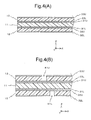
- a supporting member (hereinafter also referred to as "reinforcing layer") 11 shown in Fig. 4(A) is prepared.
- the supporting member 11 from the viewpoint of ease in handling during manufacturing steps, prepreg is preferably used.
- GHPL830 manufactured by Mitsubishi Gas Chemical Company, Inc.
- E679 manufactured by Hitachi Chemical Co., Ltd.
- R1661 manufactured by Matsushita Electric Works, Ltd.
- R1661 is preferable.
- a conductor film with a carrier (31L, 32U), an insulating layer 12, and a conductor foil 32L are prepared.
- the conductor film with a carrier (31L, 32U) is to be laminated on the surface in the -Z direction of the supporting member 11.
- the insulating layer 12 is to be laminated on the surface in the -Z direction of the conductor film with a carrier (31L, 32U).
- the conductor foil 32L is to be laminated on the surface in the -Z direction of the insulating layer 12.
- a conductor film with a carrier (31U, 33L), an insulating layer 13, and a conductor foil 33U are prepared.
- the conductor film with a carrier (31U, 33L) is to be laminated on the surface in the +Z direction of the supporting member 11.
- the insulating layer 13 is to be laminated on the surface in the +Z direction of the conductor film with a carrier (31U, 33L).
- the conductor foil 33U is to be laminated on the surface in the +Z direction of the insulating layer 13.
- the above-mentioned conductor film with a carrier can be manufactured by pressing a conductor film (32U or 33L) to adhere onto the surface of a carrier member (31L or 31U).
- the conductor film (32U or 33L) is attached to the carrier member by an adhesive, such as an adhesive that contains benzotriazole or benzotriazole derivative.
- an adhesive such as an adhesive that contains benzotriazole or benzotriazole derivative.
- VERZONE SF-310, manufactured by DAIWA KASEI K. K.
- commercially available products may be appropriately selected and used.
- Such commercially available products allow subsequent delamination of a carrier member from the conductor film.
- the examples include Micro-thin (manufactured by Mitsui Mining and Smelting Co., Ltd.), XTR (manufactured by Olin Brass), and UTC-Foil (manufactured by METFOILS AB).
- Prepreg is preferably used as the insulating layers 12 and 13.
- prepreg with a thickness of between bout 25 ⁇ m and about 100 ⁇ m such as GHPL830 (manufactured by Mitsubishi Gas Chemical Company, Inc.), E679 (manufactured by Hitachi Chemical Co., Ltd.), and R1661 (manufactured by Matsushita Electric Works, Ltd.) and the like can preferably be used in terms of the required thickness of the final product.
- those with a thickness of between about 25 ⁇ m and about 65 ⁇ m are more preferable.
- the direction of the warp WA (and therefore the weft WE) of the prepreg is preferably arranged to obliquely intersects the direction of the bending axis AX (i.e., the Y direction).
- the intersection angle ⁇ is not particularly limited. However, from the viewpoint of improvement in crack resistance at the time of bending, the angle ⁇ is preferably about 30° to about 60°. When the angle ⁇ is about 45°, it provides the greatest prevention effect on crack occurrence in insulating layers.
- the conductor film with a carrier (31L, 32U) is laminated on the reinforcing layer 11 so that the surface in the -Z direction of the reinforcing layer 11 and the surface in the +Z direction of the conductor film with a carrier (31L, 32U) are brought into contact.
- the insulating layer 12 is formed on the conductor film with a carrier (31L, 32U) so that the surface in the -Z direction of the conductor film with a carrier (31L, 3 2U) and the surface in the +Z direction of the insulating layer 12 are brought into contact.
- the conductor film with a carrier (31 U, 33L) is laminated on the reinforcing layer 11 so that the surface in the +Z direction of the reinforcing layer 11 and the surface in the - Z direction of the conductor film with a carrier (31U, 33L) are brought into contact.
- the insulating layer 13 is formed on the conductor film with a carrier (31U, 33L) so that the surface in the +Z direction of the conductor film with a carrier (31U, 33L) and the surface in the -Z direction of the insulating layer 13 are brought into contact.
- the reinforcing layer 11 and the two insulating layers laminated as shown in Fig. 4(A) are pressed under predetermined conditions, for example, at about 185°C under a pressure of about 40 kg/m 2 for about an hour, to produce a laminated body (see Fig. 4(A)).
- a CO 2 laser process is performed to form a via hole 41U.
- the opening 41U is formed so as to reach the surface in the +Z direction of the conductor layer 33L from the surface in the +Z direction of the insulating layer 13 (see Fig. 4(B)).
- a conductor layer 33U is formed on the insulating layer 13, and a black oxide forming is performed on a region of the conductor layer 33U at which the non-through via hole 41U is formed on the surface in the +Z direction of the conductor layer 33U. Subsequently, this region performed by the black oxide forming is irradiated with a laser beam having a predetermined energy from the above to form the opening 41U.
- the remaining upper surface in the +Z direction of the conductor pattern 33U, the side surface of the opening 41U and the bottom surface of the opening 41U undergo metal plating so that a plated opening is formed and a conductor film 34U is formed.
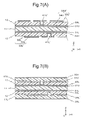
- the side surface of the opening 41L, and the bottom surface of the opening 41L undergo metal plating so that a plated opening is formed and a conductor film 34L is also formed (see Fig. 6(A)).
- the plating can be performed with a copper plating bath with a composition shown in Table 1 below.
- Copper sulfate plating bath composition Plating bath Name of compound Quantity (g/L) Copper sulfate 125 to 250 Sulfuric acid 30 to 100
- a resist layer 16U is formed on the entire surface of the conductor pattern 33U, which includes the plated via hole 41U' formed on the entire surface of a laminated body in the +Z direction.
- a resist pattern 16L is formed on the entire surface of the conductor pattern 32L, which includes the plated via hole 41L' formed on the entire surface of a laminated body in the -Z direction.
- an acrylic dry film resist such as HW440 (manufactured by Hitachi Chemical Co., Ltd.), was laminated on the whole surface of the conductor film 33U. Then, the resist is removed by a known lithography method from the regions of the conductor pattern 33U, where the conductor pattern is not formed in the +Z direction.
- an acrylic dry film resist such as HW440 (manufactured by Hitachi Chemical Co., Ltd.), for example, can be used.
- NIT1025 manufactured by Nippon Synthetic Chemical Industry Co., Ltd.
- SA-50 manufactured by DuPont
- the conductor pattern 32L undergoes a similar process with the conductor pattern 33U, then the resist is removed by a known lithography method from the regions of the conductor pattern 32L, where the conductor pattern is not formed in the -Z direction.
- etching is performed until the surface in the +Z direction of the insulating layer 13 and the surface in the -Z direction of the insulating layer 12 are exposed (see Fig. 7(A)).
- a conductor pattern is formed on the surface in the +Z direction of the insulating layer 13. Also, a plated non-through via hole 41 U' for electrically connecting the conductor pattern 34U to the conductor layer 33L is formed. Likewise, on the surface in the -Z direction of the insulating layer 12, a conductor pattern 34L' is formed, and a plated non-through via hole 41L' for electrically connecting the conductor pattern 34L' to the conductor layer 32U is formed.
- an insulating layer 17U is formed on the surface in the +Z direction of the insulating layer 13, and an insulating layer 17L is formed on the surface in the -Z direction of the insulating layer 12.
- the insulating layers 17U and 17L may be formed by lamination pressing through pin lamination.
- a material similar to that used for the insulating layers 12 and 13 can be used.
- conductor layers 35U and 35L are formed on the surface in the +Z direction of the insulating layer 17U and on the surface in the -Z direction of the insulating layer 17L, respectively (see Fig. 7(B)).
- the conductor layers 35U and 35L are formed by pressing the conductor film 35U and the conductor film 35L to adhere onto the surface in the +Z direction of the insulating layer 17U and the surface in the -Z direction of the insulating layer 17L, respectively
- Copper foil and the like can be used as the conductor films 35U and 35L.
- a conductor film with a carrier may be used to form a very thin layer of the conductor films 35U and 35L.
- the conductor film with a carrier is laminated on the corresponding insulating layer, and thereafter the carrier member is pealed off to leave the thin conductor film on the insulating layer.
- a conductor film with a carrier having a conductor film thickness of between about 3 ⁇ m and about 9 ⁇ m such as Micro-Thin (manufactured by Mitsui Mining and Smelting Co., Ltd.), XTR (manufactured by Olin Brass), UTC-Foil (manufactured by METFOILS AB) or the like.
- a conductor film with a carrier having a conductor film thickness of about 5 ⁇ m is used.
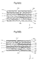
- an opening 42U is formed on the insulating layer 17U and an opening 42L is formed on the insulating layer 17L (see Fig. 8(A)).
- conductor films 36U and 36L are formed (see Fig. 8(B)).
- formation of a resist layer, and etching and removal of the resist layer are performed to form conductor pattern 36U' and 36L' (see Fig. 9).
- an ink is printed and hardened to form a coverlay layer 20U having openings 43U 1 to 43U N in a manner similar to the photolithography method.
- the cover layer 20L having openings 43L 1 to 43L N is formed.
- polyimide resin such as CKSE (manufactured by NIKKAN INDUSTRIES Co., Ltd.), for example, can be used to form the coverlay layers 20U and 20L.
- CKSE manufactured by NIKKAN INDUSTRIES Co., Ltd.
- a resist film may be laminated to form the coverlay layers.
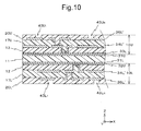
- laminated bodies 10U and 10L are formed on the respective surfaces of the reinforcing layer 11 (see Fig. 10).
- the laminated body 10U includes the conductor layer 33L, the insulating layer 13, the insulating layer 17U and the coverlay layer 20U.
- the insulating layers 13 and 17U are respectively provided with non-through via holes for inter-layer connection. Then, the via holes are through on the surface in the -Z direction of respective insulating layer.
- the laminated body 10L inc ludes the conductor layer 32U, the insulating layer 12, the insulating layer 17L and the coverlay layer 20L.
- the insulating layers 12 and 17L are respectively provided with via holes for inter-layer connection. Then, the via holes are through on the surface in the +Z direction of respective insulating layer.
- the laminated body 10U is processed in the same or similar manner.
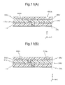
- the laminated body 10U formed on the surface in the +Z direction of the reinforcing layer 11 is separated from the reinforcing layer 11 at the interface between the carrier member 31 U and the conductor layer 33L (see Fig. 11(A)).
- nickel plating is carried out on the surface in the +Z direction of the laminated body 10U that are not covered by the coverlay layer 20U.
- the nickel plating can be conducted with a plating bath shown in Table 2 under the following conditions: pH between 4 and 5, liquid temperature of between 40°C and 60°C and current density of approximately between 2 and 6 A/dm 2 .
- Nickel electrolytic plating bath composition Plating bath Name of compound Quantity (g/L) Nickel sulfate Approximately 300 Nickel chloride Approximately 50 Boric acid Approximately 40
- gold plating can be performed on the portion that has undergone nickel plating using a plating bath with a composition shown in Table 3 under the following conditions: liquid temperature of between 20 and 25°C and current density of between 0.2 and 1.0 A/dm 2 . Note that, in Fig. 11(A), the two plated layers are illustrated as one layer.
- Au electrolytic plating bath composition Plating bath Name of compound Quantity (g/L) Gold 10 Sodium cyanide 30 to 35 Ammonia 50 to 60
- an ink is printed and hardened on the conductor layer 33L provided on the surface in the -Z direction of the laminated body 10U to form a resist layer 21L in a matter similar to the photolithography method.
- AUS series manufactured by TAIYO INK MFG. CO., LTD.
- DSR series manufactured by TAMURA Corporation
- the resist layer 21L can be formed only in the element mounting part where circuit elements will be mounted on the surface in the -Z direction of the conductor layer 33L. Alternatively, it may be formed on the entire surface except the bending part.
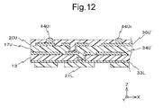
- pads 44U 1 to 44U N are formed (see Fig. 12).
- the uncovered portion of conductor layer 33L is etched to expose the surface in the -Z direction of the insulating layer 13. Then, the resist layer 21L is removed by making it come up using NaOH, thereby the conductor pattern 33L is exposed.
- the resist layer 22L is formed to cover the surface in the -Z direction of the insulating layer 13 and the surface in the -Z direction of the conductor layer 33L N . Then, by using the lithography method mentioned above, the openings 43L 1 to 43L N are formed.
- pads 45U 1 and 45U N are formed at the openings 43L 1 to 43L N , thereby completing a coreless thin type flexible printed wiring board 10.
- the manufacturing process of the flexible printed wiring board 10 described above provides an excellent yield.
- the conductor layer 33L which corresponds to an inner layer of a conductor layer laminated at the reinforcing layer 11 on the start of manufacturing, is used as the plating lead for plating, and this conductor layer 33L is processed after plating to form a conductor pattern. Therefore, the step of providing a plating lead and the step of pealing it off, which are required in the conventional art, is no longer required. This expedites the production of flexible printed wiring boards.
- the laminated body 10L formed on the surface in the -Z direction of the reinforcing layer 11 undergoes the same process as the above-described process for the laminated body 10U so that a flexible printed wiring board having the same structure as the laminated body 10U is manufactured.
- the ground pattern included in the conductor pattern 34U' in the bending part 70 is formed as a planar pattern.
- a power source pattern that imparts a ground potential in terms of alternating current may be formed in a similar planar pattern.
- signal lines by the outer layer conductor pattern 36U' can be formed to constitute a microstrip configuration in the bending part 70. Therefore, the characteristic impedance can be further stabilized.
- nickel plating and subsequent gold plating were employed.
- a different combination of the same or different metal materials may be used in the plating.
- the equal length wiring was realized by providing element mounting parts 60A and 60B on the one side.
- the other side of the flexible printed wiring board 10 may be provided with the circuit pattern 33L and the resist layer 22 to implement equal length wiring.
- the flexible printed wiring board of the present embodiment is useful as a thin type flexible printed wiring board.
- the flexible printed wiring board of the present embodiment has a stable in-line impedance when high-speed multi-pin logic LSIs and the like are mounted thereon and has excellent crack resistance.
- the method of manufacturing a flexible printed wiring board of the present embodiment is suitable for manufacturing a thin type flexible printed wiring board with an excellent yield.
- the flexible printed wiring board 10 manufactured as described above is bent (folded over) along the bending axis AX after electronic circuit chips, such as the memory elements 100A and 100B, are mounted onto the element mounting parts 60A and 60B, respectively. Then, the surface in the -X direction of the memory element 100B is affixed to the surface in the -Z direction of the flexible printed wiring board 10 with an adhesive. Subsequently, as shown in FIG. 1B, the motherboard MB and the motherboard connecting part 80 are electrically connected so that the flexible printed wiring board with the circuit chips is mounted on electronic information apparatus.
- R1661 manufactured by Matsushita Electric Works, Ltd.
- a carrier 31L, 32U
- the conductor film with a carrier 31 U, 33L
- Micro-thin manufactured by Mitsui Mining and Smelting Co., Ltd.
- XTR manufactured by Olin Brass
- UTC-Foil manufactured by METFOILS AB
- GHPL830 manufactured by Mitsubishi Gas Chemical Company, Inc.
- E679 manufactured by Hitachi Chemical Co., Ltd.
- R1661 manufactured by Matsushita Electric Works, Ltd.
- the thickness of the prepreg ranged from about 25 ⁇ m to about 65 ⁇ m.
- the prepregs used as the insulating layers 12 and 13 were arranged so that the direction of the fabric of the warp WA (and therefore the weft WE) of the prepreg obliquely intersects a line extending in the X direction to form an angle ranging between 30° and 60°, depending on Working Examples.
- the reinforcing layer 11 and the insulating layers 12 and 13 were laminated as shown in Fig. 4A and were pressed under a pressure of about 40 kg/m 2 at about 185°C for about one hour to form a laminated body.
- the black oxide forming is performed on portions at which the non-through via holes 41 U' should be formed and irradiated with a CO 2 laser beam to form the openings 41U and 41L, respectively.
- the remaining surface of the conductor pattern 33U and the interior of the opening 41U as well as the remaining surface of the conductor pattern 33L and the interior of the opening 41L underwent metal plating with a plating bath using the composition shown in Table 3 below to form the conductor films 34U and 34L.
- Copper Sulfate Plating Bath Composition Plating bath Name of compound Quantity (g/L) Copper sulfate 125 to 250 Sulfuric acid 30 to 100
- an acrylic dry film resist for example HW440 (manufactured by Hitachi Chemical Co., Ltd.), was laminated on the whole surface of conductor film 34U, and the resist is removed by a known lithography method from regions on the surface in the +Z direction of the conductor pattern 34 where a conductor pattern is not formed.
- the resist is removed from regions on the surface in the -Z direction of the conductor pattern where a conductor pattern is not formed.
- etching was performed until the surface in the +Z direction of the insulating layer 13 and the surface in the -Z direction of the insulating layer 12 were exposed.
- a conductor pattern was formed on the surface in the +Z direction of the insulating layer 13, and a plated non-through via hole 41U' for electrically connecting the conductor pattern 34U to the conductor layer 33L was formed.
- a conductor pattern was formed, and a plated non-through via hole 41L' for electrically connecting the conductor pattern 34L to the conductor layer 32U was formed.
- an insulating layer 17U was formed on the surface in the +Z direction of the insulating layer 13, and an insulating layer 17L was formed on the surface in the -Z direction of the insulating layer 12.
- Micro-Thin with thickness of approximately 5 ⁇ m, manufactured by Mitsui Mining and Smelting Co., Ltd.
- an opening 42U was formed in the insulating layer 17U and an opening 42L was formed in the insulating layer 17L.
- a plating process similar to the process mentioned above for forming the conductor layers 34U and 34L conductor films 36A were formed.
- forming of resist layer, etching and removal of resist layer from the conductor pattern was performed.
- an ink is printed and hardened to form a coverlay layer 20U having openings 43U 1 to 43U N in a manner similar to the photolithography method.
- the cover layer 20L having openings 43L, to 43L N is formed on the opposite side.
- laminated bodies 10U and 10L were formed on the respective surfaces of the reinforcing layer 11.
- the laminated body 10U formed on the surface in the +Z direction of the reinforcing layer 11 was separated from the reinforcing layer 11 at the interface between the carrier member 31U and the conductor layer 33L.
- nickel plating was carried out on the whole surface of the portions that were not covered by the coverlay layer using a plating bath with the composition shown in Table 4 under the following conditions: pH 4 to 5, liquid temperature of 40 to 60°C and current density of approximately 2 to 6 A/dm 2 .
- Nickel Electrolytic Plating Bath Composition Plating bath Name of compound Quantity (g/L) Nickel sulfate Approximately 300 Nickel chloride Approximately 50 Boric acid Approximately 40
- a resist layer 21L was formed on the conductor layer 33L provided on the surface in the -Z direction of the laminated body 10U using AUS series (manufactured by TAIYO INK MFG. CO., LTD.).
- AUS series manufactured by TAIYO INK MFG. CO., LTD.
- DSR series manufactured by TAMURA Corporation
- FIG. 12 may be used.
- the resist layer 22 is formed only in the element mounting part 60A where circuit elements is mounted on the surface in the -Z direction of the conductor layer 33L.
- soldering paste onto the openings 43U 1 to 43U N by screen printing and by solder reflowing, pads 44U 1 to 44U N were formed.
- the solder ball direct formation method may be used to form the pads.
- etching was performed to expose the surface in the -Z direction of the insulating layer 13 and the resist layer 21L was removed by making it come up using NaOH of 20 to 40 g/L, thereby conductor pattern 33L is exposed on the insulating layer 13.
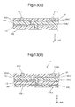
- a coverlay layer 22 was formed so as to cover the surface in the -Z direction of the exposed insulating layer 13 and the surface in the -Z direction of the conductor layer 33L, and openings 43L 1 to 43L N were formed by the lithography method (see Fig. 13(B)).
- pads 45U 1 and 45U N were formed inside the openings 43L 1 to 43 L N , thereby working examples of a coreless thin type flexible printed wiring board 10.
- the flexible printed wiring boards of comparative examples 1 to 5 were manufactured in the same way as that of the flexible printed wiring boards of working Examples 1 to 10, except that the number of the insulating layer in the bending part was three, the angle ⁇ of the warp and the weft of the glass fiber in the insulating layers relative to the bending axis was set to 0° and 45°, and then, bending tests and continuity tests were carried out. The result of these tests is shown in Table 6.
- the flexible printed wiring boards of reference examples 1 and 2 were manufactured in the same way as in the manufacture of the flexible printed wiring boards of working examples 1 to 10 except that the number of the insulating layer in the bending part was two, the angle ⁇ of the warp and the weft of the glass fiber in the insulating layers 17L and 13 relative to the bending axis was set to 25° and 65°, respectively, and that the bending angle ⁇ of the conductor pattern was set to 0°, and then bending tests and continuity tests were carried out.
- the flexible printed wiring boards of reference examples 3 and 4 were manufactured in the same way as in the manufacture of the flexible printed wiring boards of working examples 1 to 10 except that the number of the insulating layer in the bending part was two, the thickness of the insulating layers was set to 100 ⁇ m, the angle ⁇ of the warp and the weft of the glass fiber in the insulating layers relative to the bending axis was set to 45°, and that the bending angle ⁇ of the conductor pattern was set to 0°. These parameters and the results of the bending and continuity tests are listed in Table 7.
- thin-type flexible printed wiring boards of working examples 1 to 10 excelled in crack resistance.
- the flexible printed wiring board of the present invention is useful as a thin-type flexible printed wiring board and is particularly suitable for miniaturizing high-speed and large-capacity memories and the like.
- the method of manufacturing the flexible printed wiring board of the present invention is suitable for manufacturing thin-type flexible printed wiring boards that have superior crack resistance and has an excellent yield.
Landscapes
- Engineering & Computer Science (AREA)
- Microelectronics & Electronic Packaging (AREA)
- Manufacturing & Machinery (AREA)
- Structure Of Printed Boards (AREA)
Abstract
Description
- This invention relates to a flexible printed wiring board, and more particularly, to a flexible printed wiring board having an element mounting part where circuit elements are mounted and a bending part to be bent around a bending axis.
- Recent progress in information society invites rapid increase in information quantity, and rapid exchange and transmission of a large capacity of information data are required. Consequently, integration in electronic circuit elements has been improved, and enhancement in performance, enhancement in function and enhancement in integration are in progress for electronic information apparatus. In such a trend, printed wiring boards used in electronic information apparatus are also undergoing enhancement in thinning, miniaturization, and intensified function, and various proposals have been made for flexible printed wiring boards as well. (See Patent Document Nos. 1-5)
- Among such flexible printed wiring boards, with respect to those with memory elements mounted thereon, a new structure with an increased memory capacity and speed has been proposed and put into practical use. For example, flexible printed wiring boards in which a chip size package (CSP) is mountable to both surfaces have been developed.
- Such a flexible printed wiring board with CSPs mounted on both surfaces is arranged to have a layered structure throughout the substrate surface, as shown in Fig. 15, typically consisting of three conductor layers (
PT 1 to PT3), two insulating layers (1N and IN2) isolating these conductor layers, and two coverlay layers (CL1 and CL2) (hereafter referred to as "related art example"). In addition, in a flexible printed wiring board of the related art example, memory elements, for example, are mounted on both surfaces of an element mounting part 60' as shown in Fig. 15. A bending part 70' is bent around the bending axis AX', so that a motherboard connecting part 80', which is formed at the top surface on the other end, is made in electric contact with the motherboard MB (Fig. 15). Consequently, the efficiency in implementation of memory elements on a motherboard can be improved. -
- [Patent Document 1]
Japanese Patent Laid-Open No. 1993-243741 - [Patent Document 2]
Japanese Patent Laid-Open No. 1994-216537 - [Patent Document 3]
Japanese Patent Laid-Open No. 1996-130351 - [Patent Document 4]
Japanese Patent Laid-Open No. 1996-125342 - [Patent Document 5]
Japanese Patent Laid-Open No. 1995-202358 - When the above described related art example of a flexible printed wiring board is bent along the bending axis, tensile stress is applied to the outer side, while compressive stress is applied to the inner side. In addition, depending on the curvature at the time of bending, cracks may occur in the insulating layers. Therefore, it is preferable to decrease the curvature of bending; but the decrease in the curvature of bending would impede high-density mounting of memory elements.
- Therefore, currently, a flexible printed wiring board with improved bending-withstanding properties is desired.
- The present invention has been conceived in view of the above described situation. An object of the present invention is to provide a flexible printed wiring board that has improved crack resistance.
- A flexible printed wiring board according to a preferred embodiment of the present invention comprises an element mounting part where circuit elements are mounted and a bending part to be bent around the bending axis. An inner conductor layer is formed on the inside of the board. In the element mounting part, element mounting part conductor layers are formed on both surfaces at outer sides of the wiring board, respectively, and in the bending part, a bending part conductor layer is formed only on the surface on the outer side that faces the exterior when the wiring board is bent.
- In this case, in the above described element mounting part, the element mounting part conductor layers are formed on both surfaces at the outer sides of the wiring board, respectively. In contrast, in the bending part, the bending part conductor layer is formed only on the side that faces the exterior when it is bent. Therefore, as compared with the related art example described above, this configuration allows a reduction of the number of conductor layers in the bending part by one and the number of coverlay layer by one as well. Thus, by reducing the number of layers in the bending part, the total thickness can be made thin as compared with the related art flexible printed wiring boards. Consequently, when the flexible wiring board is bent at the same curvature, the stress is reduced, and therefore crack resistance is improved.
- In addition, in the above described inner layer conductor layer, a conductor pattern that imparts a ground potential in terms of alternating current may be formed. Thus, by forming a conductor pattern to impart a ground potential in terms of alternating current as an interior layer conductor layer, the characteristic impedance of a signal circuit pattern (also referred to as "outer layer conductor pattern") formed at the side that faces the exterior can be stabilized even when the flexible printed wiring board is bent along the bending axis.
- In particular, in the inner conductor layer in the bending part, a conductor pattern to impart the ground potential in terms of alternating current may be formed in a plane pattern. In this case, signal lines of the outer layer conductor pattern in the bending part can be formed to constitute a microstrip configuration, thereby further stabilizing the characteristic impedance.
- The insulating layer formed between the above described conductor patterns are preferably made of fiber-reinforced plastic. As examples of such fiber-reinforced plastics, there are mentioned fiber-glass reinforced plastics (GFRP), carbon fiber reinforced plastics (CFRP) and the like. More specifically, glass-fiber-reinforced epoxy, glass-fiber-reinforced polyester resin and the like may be used.
- The thickness of the above described insulating layer is preferably between about 25 µm and about 65 µm. In this case, when the thickness of the above described insulating layer is less than about 25 µm, it is difficult to form an insulating layer with a uniform thickness, while when the thickness exceeds about 65 µm, preferable crack resistance may not be obtained.
- In addition, the warp and the weft contained in the above described fiber-reinforced plastic preferably extend in the directions intersecting the direction of the above described bending axis by an angle of about 30° or more and about 60° or less. With this configuration, when the wiring board is bent, the warp and the weft mechanically cooperate to improve crack resistance.
- The signal conductive pattern formed in the above described bending part conductor layer preferably extends in the direction that is obliquely disposed relative to the direction of the above described bending axis. This way, when the bending part is bent around the bending axis, the crack-prevention performance of the signal conductor pattern is further improved and the occurrence of cracks can be further reduced.
- Note that, the above described circuit element can be a memory element. In this case, high density implementation of memory elements, which has been desired more and more in recent years, becomes possible.
- As has been described above, according to the present invention, one advantage of the present invention is that a flexible printed wiring board with improved crack resistance can be provided.
-
- Fig. 1 illustrates a construction of a flexible printed wiring board according to one embodiment of the present invention;
- Fig. 2 is a cross-sectional view of a flexible printed wiring board according to an embodiment of present invention;
- Fig. 3 is a schematic view illustrating the wiring direction of the signal conductor pattern of a flexible printed wiring board according to manufacturing of an embodiment of the present invention;
- Fig. 4 is a cross-sectional view (No.1) illustrating manufacturing steps of a flexible printed wiring board according to an embodiment of the present invention;
- Fig. 5 is a schematic view for showing the directions of the warp and the weft of the fiber-reinforced fabric in an insulating layer of a flexible printed wiring board according to an embodiment of the present invention;
- Fig. 6 is a cross-sectional view (No.2) illustrating manufacturing steps of a flexible printed wiring board according to an embodiment of the present invention;
- Fig. 7 is a cross-sectional view (No.3) illustrating manufacturing steps of a flexible printed wiring board according to an embodiment of the present invention;
- Fig. 8 is a cross-sectional view (No.4) illustrating manufacturing steps of a flexible printed wiring board according to an embodiment of the present invention;
- Fig. 9 is a cross-sectional view (No.5) illustrating the manufacture of a flexible printed wiring board according to an embodiment of the present invention;
- Fig. 10 is a cross-sectional view (No.6) illustrating the manufacture of a flexible printed wiring board according to an embodiment of the present invention;
- Fig. 11 is a cross-sectional view (No.7) illustrating manufacturing steps of a flexible printed wiring board according to an embodiment of the present invention;
- Fig. 12 is a cross-sectional view (No.8) illustrating a manufacturing step of a flexible printed wiring board according to an embodiment of the present invention;
- Fig. 13 is a cross-sectional view (No.9) illustrating manufacturing steps of a flexible printed wiring board according to an embodiment of the present invention;
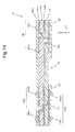
- Fig. 14 is a cross-sectional view showing a construction of a flexible printed wiring board according to an embodiment of the present invention; and
- Fig. 15 illustrates a construction of a flexible printed wiring board according to the related art.
- One embodiment of the present invention will be described with reference to Fig. 1-Fig. 13. Fig. 1 shows a configuration of a flexible printed
wiring board 10 according to an embodiment of the present invention as a perspective view. Fig.1(A) is a perspective view thereof. Fig. 1(B) is an XZ side view of the flexible printedwiring board 10 which is bent at a bending part along the bending axis AX and is attached to a motherboard MB. - In this embodiment, on the upper surface in the +Z direction of the flexible printed
wiring board 10 shown in Fig. 1(A), pads 44U1 to 44UN for mounting acircuit element 100A and pads 47L1 to 47LN are provided, and pads 44U1 to 44UN and pads 47L1 to 47LN are electrically connected, respectively, for example. - In addition, although not shown in Fig. 1(A), on the lower surface (i.e., the surface facing in the -Z direction) of the flexible printed
wiring board 10, pads 45U1 to 45UN for mounting acircuit element 100B are formed at locations that correspond to the pads 44U1 to 44UN. For example, these pads 45U1 to 45UN and pads 47L1 to 47LN are also electrically connected, respectively. - Note that, in the present embodiment, both
circuit element 100A andcircuit element 100B can be memory elements of the same type. - As shown in Fig. 1, the
element 100A is mounted on the upper surface and the element 1008 is mounted on the lower surface of the flexible printedwiring board 10. In mounting the flexible printedwiring board 10 on a host board, such as a mother board, the flexible printedwiring board 10 is bent around the bending axis AX, and is mounted on the motherboard MB, as shown in Fig. 1(B). In this case, thecircuit element 100B of the flexible printedwiring board 10 is bonded via abonding layer 90 to a surface of the folded-over portion of the flexible printed wiring board, which is opposite to the surface having the pads 47L1 to 47LN. - Fig. 2 shows an XZ cross-sectional view of the flexible printed
wiring board 10 of the present embodiment. As shown in Fig. 2, the flexible printedwiring board 10 of the present embodiment includes anelement mounting parts element mounting part 60" collectively) where thecircuit elements part 70 where this flexible printed wiring board is bent around the bending axis AX, and amotherboard connecting part 80, which is to be connected to a motherboard. - In addition, the flexible printed
wiring board 10 includes, in theelement mounting part 60, (a) an insulatinglayer 13, (b) an insulatinglayer 17U formed on a surface in the +Z direction side of the insulatinglayer 13, (c) an insulatinglayer 20U, which is the outmost layer formed on a surface in the +Z direction side of the insulatinglayer 17U and (d) an insulatinglayer 22 formed on a surface in the -Z direction side of the insulatinglayer 13. In this embodiment, the insulatinglayers layer 22 is not formed in the bendingpart 70, the bendingpart 70 includes the layers (a) to (c), but does not include the insulating layer 22 (d). - In addition, the flexible printed
wiring board 10 includes (c) aconductor pattern 34U' formed on the surface in the +Z direction of the insulatinglayer 13, (d) afirst conductor pattern 36U', which is a signal line pattern, formed on the surface in the +Z direction of the insulatinglayer 17U and (e) asecond conductor pattern 33L, which is a signal line pattern, formed on the surface in the -Z direction of the insulatinglayer 13 in theelement mounting part 60. - In this embodiment, this
conductor pattern 34U' includes a conductor pattern to impart a ground potential in terms of alternating current (hereinafter also referred to as "ground pattern" or "GNP"), and additionally includes circuit patterns formed at through holes, which intersects ground pattern and each layer. The GNP may be formed in a solid pattern to cover substantially the entire area at the bendingpart 70. Thefirst conductor pattern 36U' includes a power supply pattern as well. Note that, in the bendingpart 70, thefirst conductor pattern 36U' is arranged to extend in the direction that intersects the bending axis AX (the Y direction) at an angle θ. - Subsequently, the GNP is formed as a planar pattern which is made by a conductive material and substantially covers the entire area of the insulating
layer 13 in the bendingpart 70. In this embodiment, as shown in Fig. 3, conductor patterns P1 to PN (which electrically connect the pads 44U1- 44UN to 47L1 - 47LN, respectively, for example) are not disposed parallel to the X direction, but intersect a virtual line extending in the Y direction at angle θ. - Particularly, the ground pattern in the
conductor pattern 34U', which is arranged in the bendingpart 70, is formed to cover the substantially entire area as the planar ground pattern. Since signal lines of thesignal line pattern 33L, which forms the outer conductive pattern line, in the bendingpart 70 can be made as a microstrip configuration, the characteristic impedance can be stabilized. - Moreover, the flexible printed
wiring board 10 includes (f) non-through via holes on the surface in the - Z direction of the insulatinglayers first conductor pattern 36U', and thesecond conductor pattern 33L. - Note that, although not depicted in Fig. 2, non-through via holes are also provided in the
motherboard connecting part 80 to provide interconnections between the GNP (conductor pattern 34U') and thefirst conductor pattern 36U'. - Pads 44U1 to 44UN for mounting
circuit element 100A are formed on the surface in the + Z direction of thefirst conductor pattern 36U' of the flexible printed wiring board 10.In addition, pads 45U1 to 45UN for mounting anothercircuit element 100B are formed on the surface in the - Z direction of the secondconductive pattern 33L. - In this embodiment, the length of wiring pattern connecting the pads 44Uj (j = 1 to N) with the pads 47Lj and the length of wiring pattern connecting the pads 45Uj with the pads 47Lj can be made respectively the same to implement equal length wiring.
- As the material of the insulating
layers layers - In addition, as for the insulating
layers - As the material for the
conductor patterns - Next, manufacturing steps of the flexible printed
wiring board 10 will be described. - At first, a supporting member (hereinafter also referred to as "reinforcing layer") 11 shown in Fig. 4(A) is prepared. In this embodiment, as the supporting
member 11, from the viewpoint of ease in handling during manufacturing steps, prepreg is preferably used. Specifically, GHPL830 (manufactured by Mitsubishi Gas Chemical Company, Inc.), E679 (manufactured by Hitachi Chemical Co., Ltd.), R1661 (manufactured by Matsushita Electric Works, Ltd.) and the like can be used. In terms of costs as well as dimensional stability, R1661 is preferable. - Next, a conductor film with a carrier (31L, 32U), an insulating
layer 12, and aconductor foil 32L are prepared. The conductor film with a carrier (31L, 32U) is to be laminated on the surface in the -Z direction of the supportingmember 11. The insulatinglayer 12 is to be laminated on the surface in the -Z direction of the conductor film with a carrier (31L, 32U). Theconductor foil 32L is to be laminated on the surface in the -Z direction of the insulatinglayer 12. In addition, a conductor film with a carrier (31U, 33L), an insulatinglayer 13, and aconductor foil 33U are prepared. The conductor film with a carrier (31U, 33L) is to be laminated on the surface in the +Z direction of the supportingmember 11. The insulatinglayer 13 is to be laminated on the surface in the +Z direction of the conductor film with a carrier (31U, 33L). Theconductor foil 33U is to be laminated on the surface in the +Z direction of the insulatinglayer 13. - The above-mentioned conductor film with a carrier can be manufactured by pressing a conductor film (32U or 33L) to adhere onto the surface of a carrier member (31L or 31U). The conductor film (32U or 33L) is attached to the carrier member by an adhesive, such as an adhesive that contains benzotriazole or benzotriazole derivative. For example, VERZONE (SF-310, manufactured by DAIWA KASEI K. K.) and the like can be used so that the resulting film can be delaminated at a later time. In addition, commercially available products may be appropriately selected and used.
- Such commercially available products allow subsequent delamination of a carrier member from the conductor film. The examples include Micro-thin (manufactured by Mitsui Mining and Smelting Co., Ltd.), XTR (manufactured by Olin Brass), and UTC-Foil (manufactured by METFOILS AB).
- Prepreg is preferably used as the insulating
layers - In this embodiment, as shown in Fig. 5, in the prepreg used as the insulating
layers - The intersection angle φ is not particularly limited. However, from the viewpoint of improvement in crack resistance at the time of bending, the angle φ is preferably about 30° to about 60°. When the angle φ is about 45°, it provides the greatest prevention effect on crack occurrence in insulating layers.
- Referring to Fig. 4, the conductor film with a carrier (31L, 32U) is laminated on the reinforcing
layer 11 so that the surface in the -Z direction of the reinforcinglayer 11 and the surface in the +Z direction of the conductor film with a carrier (31L, 32U) are brought into contact. The insulatinglayer 12 is formed on the conductor film with a carrier (31L, 32U) so that the surface in the -Z direction of the conductor film with a carrier (31L, 3 2U) and the surface in the +Z direction of the insulatinglayer 12 are brought into contact. - Then, the conductor film with a carrier (31 U, 33L) is laminated on the reinforcing
layer 11 so that the surface in the +Z direction of the reinforcinglayer 11 and the surface in the - Z direction of the conductor film with a carrier (31U, 33L) are brought into contact. The insulatinglayer 13 is formed on the conductor film with a carrier (31U, 33L) so that the surface in the +Z direction of the conductor film with a carrier (31U, 33L) and the surface in the -Z direction of the insulatinglayer 13 are brought into contact. - The reinforcing
layer 11 and the two insulating layers laminated as shown in Fig. 4(A) are pressed under predetermined conditions, for example, at about 185°C under a pressure of about 40 kg/m2 for about an hour, to produce a laminated body (see Fig. 4(A)). - Subsequently, a CO2 laser process is performed to form a via
hole 41U. Theopening 41U is formed so as to reach the surface in the +Z direction of theconductor layer 33L from the surface in the +Z direction of the insulating layer 13 (see Fig. 4(B)). - To form the
opening 41U, first, aconductor layer 33U is formed on the insulatinglayer 13, and a black oxide forming is performed on a region of theconductor layer 33U at which the non-through viahole 41U is formed on the surface in the +Z direction of theconductor layer 33U. Subsequently, this region performed by the black oxide forming is irradiated with a laser beam having a predetermined energy from the above to form theopening 41U. - In forming a via
hole 41L on the surface in the -Z direction of the insulatinglayer 12, the similar process is implemented (see Fig. 4(B)). - The remaining upper surface in the +Z direction of the
conductor pattern 33U, the side surface of theopening 41U and the bottom surface of theopening 41U (that is, the exposed surface in the +Z direction of theconductor pattern 33L inside theopening 41U) undergo metal plating so that a plated opening is formed and aconductor film 34U is formed. Similarly, the side surface of theopening 41L, and the bottom surface of theopening 41L undergo metal plating so that a plated opening is formed and aconductor film 34L is also formed (see Fig. 6(A)). - The plating can be performed with a copper plating bath with a composition shown in Table 1 below.
-
TABLE 1: Copper sulfate plating bath composition Plating bath Name of compound Quantity (g/L) Copper sulfate 125 to 250 Sulfuric acid 30 to 100 - Subsequently, referring to Fig. 6(A), a resist
layer 16U is formed on the entire surface of theconductor pattern 33U, which includes the plated viahole 41U' formed on the entire surface of a laminated body in the +Z direction. Similarly, a resistpattern 16L is formed on the entire surface of theconductor pattern 32L, which includes the plated viahole 41L' formed on the entire surface of a laminated body in the -Z direction. - Subsequently, an acrylic dry film resist, such as HW440 (manufactured by Hitachi Chemical Co., Ltd.), was laminated on the whole surface of the
conductor film 33U. Then, the resist is removed by a known lithography method from the regions of theconductor pattern 33U, where the conductor pattern is not formed in the +Z direction. - As the resist layer, an acrylic dry film resist, such as HW440 (manufactured by Hitachi Chemical Co., Ltd.), for example, can be used. Moreover, NIT1025 (manufactured by Nippon Synthetic Chemical Industry Co., Ltd.), SA-50 (manufactured by DuPont) and the like can also be used.
- The
conductor pattern 32L undergoes a similar process with theconductor pattern 33U, then the resist is removed by a known lithography method from the regions of theconductor pattern 32L, where the conductor pattern is not formed in the -Z direction. - Subsequently, by employing a tenting process using an etching solution including copper (II) chloride or the like, the solder delamination process using a metal resist, or the micro-etching process suitable for fine pattern forming or the like, etching is performed until the surface in the +Z direction of the insulating
layer 13 and the surface in the -Z direction of the insulatinglayer 12 are exposed (see Fig. 7(A)). - As a result, a conductor pattern is formed on the surface in the +Z direction of the insulating
layer 13. Also, a plated non-through viahole 41 U' for electrically connecting theconductor pattern 34U to theconductor layer 33L is formed. Likewise, on the surface in the -Z direction of the insulatinglayer 12, aconductor pattern 34L' is formed, and a plated non-through viahole 41L' for electrically connecting theconductor pattern 34L' to theconductor layer 32U is formed. - Next, an insulating
layer 17U is formed on the surface in the +Z direction of the insulatinglayer 13, and an insulatinglayer 17L is formed on the surface in the -Z direction of the insulatinglayer 12. In this embodiment, the insulatinglayers layers layers layer 17U and on the surface in the -Z direction of the insulatinglayer 17L, respectively (see Fig. 7(B)). - The conductor layers 35U and 35L are formed by pressing the
conductor film 35U and theconductor film 35L to adhere onto the surface in the +Z direction of the insulatinglayer 17U and the surface in the -Z direction of the insulatinglayer 17L, respectively - Copper foil and the like can be used as the
conductor films conductor films - In this embodiment, it is preferable to use a conductor film with a carrier having a conductor film thickness of between about 3 µm and about 9 µm, such as Micro-Thin (manufactured by Mitsui Mining and Smelting Co., Ltd.), XTR (manufactured by Olin Brass), UTC-Foil (manufactured by METFOILS AB) or the like. In this embodiment mentioned above, a conductor film with a carrier having a conductor film thickness of about 5 µm is used.
- Subsequently, using a process similar to the process for forming the above-described
openings 41U, anopening 42U is formed on the insulatinglayer 17U and anopening 42L is formed on the insulatinglayer 17L (see Fig. 8(A)). Then, using a plating process similar to the plating process described above,conductor films conductor pattern 36U' and 36L' (see Fig. 9). - Next, referring to Fig. 10, an ink is printed and hardened to form a
coverlay layer 20U having openings 43U1 to 43UN in a manner similar to the photolithography method. Likewise, thecover layer 20L having openings 43L1 to 43LN is formed. In this embodiment, polyimide resin such as CKSE (manufactured by NIKKAN INDUSTRIES Co., Ltd.), for example, can be used to form the coverlay layers 20U and 20L. In the alternative, instead af an ink, a resist film may be laminated to form the coverlay layers. - Consequently,
laminated bodies 10U and 10L are formed on the respective surfaces of the reinforcing layer 11 (see Fig. 10). In this embodiment, as shown in Fig. 10, the laminated body 10U includes theconductor layer 33L, the insulatinglayer 13, the insulatinglayer 17U and thecoverlay layer 20U. The insulating layers 13 and 17U are respectively provided with non-through via holes for inter-layer connection. Then, the via holes are through on the surface in the -Z direction of respective insulating layer. - As shown in Fig. 10, the
laminated body 10L inc ludes theconductor layer 32U, the insulatinglayer 12, the insulatinglayer 17L and thecoverlay layer 20L. The insulating layers 12 and 17L are respectively provided with via holes for inter-layer connection. Then, the via holes are through on the surface in the +Z direction of respective insulating layer. - The following steps are described with reference to the laminated body 10U. The
laminated body 10L is processed in the same or similar manner. The laminated body 10U formed on the surface in the +Z direction of the reinforcinglayer 11 is separated from the reinforcinglayer 11 at the interface between thecarrier member 31 U and theconductor layer 33L (see Fig. 11(A)). - Subsequently, using the
conductor layer 33L, which is formed on the surface in the -Z direction of the laminated body 10U, as a plating lead, nickel plating is carried out on the surface in the +Z direction of the laminated body 10U that are not covered by thecoverlay layer 20U. In this embodiment, the nickel plating can be conducted with a plating bath shown in Table 2 under the following conditions: pH between 4 and 5, liquid temperature of between 40°C and 60°C and current density of approximately between 2 and 6 A/dm2. -
TABLE 2: Nickel electrolytic plating bath composition Plating bath Name of compound Quantity (g/L) Nickel sulfate Approximately 300 Nickel chloride Approximately 50 Boric acid Approximately 40 - Subsequently, gold plating can be performed on the portion that has undergone nickel plating using a plating bath with a composition shown in Table 3 under the following conditions: liquid temperature of between 20 and 25°C and current density of between 0.2 and 1.0 A/dm2. Note that, in Fig. 11(A), the two plated layers are illustrated as one layer.
-
TABLE 3: Au electrolytic plating bath composition Plating bath Name of compound Quantity (g/L) Gold 10 Sodium cyanide 30 to 35 Ammonia 50 to 60 - After completion of the above-described plating process, an ink is printed and hardened on the
conductor layer 33L provided on the surface in the -Z direction of the laminated body 10U to form a resistlayer 21L in a matter similar to the photolithography method. In this embodiment, AUS series (manufactured by TAIYO INK MFG. CO., LTD.) and DSR series (manufactured by TAMURA Corporation), for example, can be used to form the resist layer. - Note that, the resist
layer 21L can be formed only in the element mounting part where circuit elements will be mounted on the surface in the -Z direction of theconductor layer 33L. Alternatively, it may be formed on the entire surface except the bending part. - Subsequently, by disposing soldering paste onto the openings 43U1 to 43UN by screen printing and subsequently performing a solder reflow process, or by using the solder ball direct mounting method or the like, pads 44U1 to 44UN are formed (see Fig. 12).
- Next, as shown in Fig. 13(A), by a tenting method, the uncovered portion of
conductor layer 33L is etched to expose the surface in the -Z direction of the insulatinglayer 13. Then, the resistlayer 21L is removed by making it come up using NaOH, thereby theconductor pattern 33L is exposed. - Subsequently, the resist layer 22L is formed to cover the surface in the -Z direction of the insulating
layer 13 and the surface in the -Z direction of theconductor layer 33LN. Then, by using the lithography method mentioned above, the openings 43L1 to 43LN are formed. - Subsequently, by a process similar to the process described above, pads 45U1 and 45UN are formed at the openings 43L1 to 43LN, thereby completing a coreless thin type flexible printed
wiring board 10. - The manufacturing process of the flexible printed
wiring board 10 described above provides an excellent yield. - Moreover, in the above-described manufacturing method, the
conductor layer 33L, which corresponds to an inner layer of a conductor layer laminated at the reinforcinglayer 11 on the start of manufacturing, is used as the plating lead for plating, and thisconductor layer 33L is processed after plating to form a conductor pattern. Therefore, the step of providing a plating lead and the step of pealing it off, which are required in the conventional art, is no longer required. This expedites the production of flexible printed wiring boards. - Note that, the
laminated body 10L formed on the surface in the -Z direction of the reinforcinglayer 11 undergoes the same process as the above-described process for the laminated body 10U so that a flexible printed wiring board having the same structure as the laminated body 10U is manufactured. - In the above described embodiment, the ground pattern included in the
conductor pattern 34U' in the bendingpart 70 is formed as a planar pattern. Alternatively, a power source pattern that imparts a ground potential in terms of alternating current may be formed in a similar planar pattern. In this case, signal lines by the outerlayer conductor pattern 36U' can be formed to constitute a microstrip configuration in the bendingpart 70. Therefore, the characteristic impedance can be further stabilized. - Moreover, as for the metal plating used for the above-described manufacture of the flexible printed wiring board, nickel plating and subsequent gold plating were employed. However, a different combination of the same or different metal materials may be used in the plating.
- Note that, in the above described embodiment, as shown in Fig. 2, the equal length wiring was realized by providing
element mounting parts wiring board 10 may be provided with thecircuit pattern 33L and the resistlayer 22 to implement equal length wiring. - The flexible printed wiring board of the present embodiment is useful as a thin type flexible printed wiring board. In particular, the flexible printed wiring board of the present embodiment has a stable in-line impedance when high-speed multi-pin logic LSIs and the like are mounted thereon and has excellent crack resistance.
- Moreover, the method of manufacturing a flexible printed wiring board of the present embodiment is suitable for manufacturing a thin type flexible printed wiring board with an excellent yield.
- The flexible printed
wiring board 10 manufactured as described above is bent (folded over) along the bending axis AX after electronic circuit chips, such as thememory elements element mounting parts memory element 100B is affixed to the surface in the -Z direction of the flexible printedwiring board 10 with an adhesive. Subsequently, as shown in FIG. 1B, the motherboard MB and themotherboard connecting part 80 are electrically connected so that the flexible printed wiring board with the circuit chips is mounted on electronic information apparatus. - Working examples of the present invention will now be described in detail. However, the present invention will not be limited by these examples in any ways.
- As the reinforcing
layer 11, R1661 (manufactured by Matsushita Electric Works, Ltd.) was used. In forming the conductor film with a carrier (31L, 32U) to be laminated on the surface in the -Z direction of the reinforcinglayer 11, the conductor foils 33L to be laminated on the surface in the -Z direction of the insulatinglayers 13 and on the surface in the -Z direction of the reinforcinglayer 12, and the conductor film with a carrier (31 U, 33L) to be laminated on the surface in the +Z direction of the reinforcinglayer 11, Micro-thin (manufactured by Mitsui Mining and Smelting Co., Ltd.) was used. For these conductor films with a carrier, XTR (manufactured by Olin Brass) or UTC-Foil (manufactured by METFOILS AB) may also be used in place of Micro-thin. - As the insulating
layers - The prepregs used as the insulating
layers - The reinforcing
layer 11 and the insulatinglayers - Subsequently, on the insulating
layers holes 41 U' should be formed and irradiated with a CO2 laser beam to form theopenings - Next, the remaining surface of the
conductor pattern 33U and the interior of theopening 41U as well as the remaining surface of theconductor pattern 33L and the interior of theopening 41L underwent metal plating with a plating bath using the composition shown in Table 3 below to form theconductor films -
TABLE 4: Copper Sulfate Plating Bath Composition Plating bath Name of compound Quantity (g/L) Copper sulfate 125 to 250 Sulfuric acid 30 to 100 - Subsequently, an acrylic dry film resist, for example HW440 (manufactured by Hitachi Chemical Co., Ltd.), was laminated on the whole surface of
conductor film 34U, and the resist is removed by a known lithography method from regions on the surface in the +Z direction of the conductor pattern 34 where a conductor pattern is not formed. - In a similar fashion on the whole surface of the
conductor pattern 34L, the resist is removed from regions on the surface in the -Z direction of the conductor pattern where a conductor pattern is not formed. - Subsequently, by employing a tenting process using copper (II) chloride, the solder delamination process using a metal resist, or the micro-etching process suitable for fine pattern forming, etching was performed until the surface in the +Z direction of the insulating
layer 13 and the surface in the -Z direction of the insulatinglayer 12 were exposed. - Accordingly, a conductor pattern was formed on the surface in the +Z direction of the insulating
layer 13, and a plated non-through viahole 41U' for electrically connecting theconductor pattern 34U to theconductor layer 33L was formed. Likewise, on the surface in the - Z direction of the insulatinglayer 12, a conductor pattern was formed, and a plated non-through viahole 41L' for electrically connecting theconductor pattern 34L to theconductor layer 32U was formed. - Next, by lamination pressing through pin lamination, an insulating
layer 17U was formed on the surface in the +Z direction of the insulatinglayer 13, and an insulatinglayer 17L was formed on the surface in the -Z direction of the insulatinglayer 12. Subsequently, by pressing Micro-Thin (with thickness of approximately 5 µm, manufactured by Mitsui Mining and Smelting Co., Ltd.) to adhere onto the surface in the +Z direction of the insulatinglayer 17U and onto the surface in the -Z direction of the insulatinglayer 17L, respectively, and then by pealing off the carrier member, conductor layers 35U and 35L were formed. - Subsequently, using a process similar to the process for forming the
openings 41U, anopening 42U was formed in the insulatinglayer 17U and anopening 42L was formed in the insulatinglayer 17L. Subsequently, using a plating process similar to the process mentioned above for forming the conductor layers 34U and 34L, conductor films 36A were formed. Then, using a process similar to the process mentioned above, forming of resist layer, etching and removal of resist layer from the conductor pattern was performed. - Subsequently, an ink is printed and hardened to form a
coverlay layer 20U having openings 43U1 to 43UN in a manner similar to the photolithography method. Likewise, thecover layer 20L having openings 43L, to 43LN is formed on the opposite side. As a result,laminated bodies 10U and 10L were formed on the respective surfaces of the reinforcinglayer 11. - As described above, the laminated body 10U formed on the surface in the +Z direction of the reinforcing
layer 11 was separated from the reinforcinglayer 11 at the interface between thecarrier member 31U and theconductor layer 33L. - Subsequently, using the
conductor layer 33L, which has been formed on the surface in the -Z direction of the insulatinglayer 13, as the plating lead, nickel plating was carried out on the whole surface of the portions that were not covered by the coverlay layer using a plating bath with the composition shown in Table 4 under the following conditions: pH 4 to 5, liquid temperature of 40 to 60°C and current density of approximately 2 to 6 A/dm2. -
TABLE 5: Nickel Electrolytic Plating Bath Composition Plating bath Name of compound Quantity (g/L) Nickel sulfate Approximately 300 Nickel chloride Approximately 50 Boric acid Approximately 40 - Subsequently, gold plating was performed on the portions that have undergone nickel plating using a plating bath with the composition shown in Table 5 under the following conditions: liquid temperature of 20 to 25°C and current density of 0.2 to 1.0 A/dm2.
-
TABLE 6: Au Electrolytic Plating Bath Composition Plating bath Name of compound Quantity (g/L) Gold 10 Sodium cyanide 30 to 35 Ammonia 50 to 60 - After the completion of the above-described plating process, a resist
layer 21L was formed on theconductor layer 33L provided on the surface in the -Z direction of the laminated body 10U using AUS series (manufactured by TAIYO INK MFG. CO., LTD.). In stead of AUS series, DSR series (manufactured by TAMURA Corporation) (FIG. 12) may be used. - Note that, in Working Examples 1 to 10 and Reference Examples 1 to 4, the resist
layer 22 is formed only in theelement mounting part 60A where circuit elements is mounted on the surface in the -Z direction of theconductor layer 33L. - Subsequently, by disposing a soldering paste onto the openings 43U1 to 43UN by screen printing and by solder reflowing, pads 44U1 to 44UN were formed. Instead of using screen printing, the solder ball direct formation method may be used to form the pads.
- Next, by a tenting method, etching was performed to expose the surface in the -Z direction of the insulating
layer 13 and the resistlayer 21L was removed by making it come up using NaOH of 20 to 40 g/L, therebyconductor pattern 33L is exposed on the insulatinglayer 13. - Subsequently, a
coverlay layer 22 was formed so as to cover the surface in the -Z direction of the exposed insulatinglayer 13 and the surface in the -Z direction of theconductor layer 33L, and openings 43L1 to 43LN were formed by the lithography method (see Fig. 13(B)). - Subsequently, in a manner similar to that mentioned above, pads 45U1 and 45UN were formed inside the openings 43L1 to 43 LN, thereby working examples of a coreless thin type flexible printed
wiring board 10. - Bending tests and continuity tests were carried out for flexible printed wiring boards of Working Examples 1 to 10 with impedance of 50 Ω (design value), which were manufactured as described above. The MIT (flexural fatigue resistance) test of JIS5016 was adopted as the bending test, and occurrence of cracks in insulating layers and conductor layers were examined. In addition, the continuity test was conducted with a TCT (thermo cycle test) tester, and the continuity was examined after predetermined numbers of repetition of the thermal cycle consisting of raising the temperature from -55°C to 125°C in 30 minutes and lowering the temperature in the reverse manner. The continuity was evaluated at 50 cycles and 100 cycles. The lost continuity results were indicated as NG. The test results for Working Examples 1-10 are shown in Table 6.
- The flexible printed wiring boards of comparative examples 1 to 5 were manufactured in the same way as that of the flexible printed wiring boards of working Examples 1 to 10, except that the number of the insulating layer in the bending part was three, the angle φ of the warp and the weft of the glass fiber in the insulating layers relative to the bending axis was set to 0° and 45°, and then, bending tests and continuity tests were carried out. The result of these tests is shown in Table 6.
- The flexible printed wiring boards of reference examples 1 and 2 were manufactured in the same way as in the manufacture of the flexible printed wiring boards of working examples 1 to 10 except that the number of the insulating layer in the bending part was two, the angle φ of the warp and the weft of the glass fiber in the insulating
layers - In addition, the flexible printed wiring boards of reference examples 3 and 4 were manufactured in the same way as in the manufacture of the flexible printed wiring boards of working examples 1 to 10 except that the number of the insulating layer in the bending part was two, the thickness of the insulating layers was set to 100 µm, the angle φ of the warp and the weft of the glass fiber in the insulating layers relative to the bending axis was set to 45°, and that the bending angle θ of the conductor pattern was set to 0°. These parameters and the results of the bending and continuity tests are listed in Table 7.
-
[Table 7] Classification classification Conductor layer counts Conductor layer Thickness of insulating layer (µm) Angle of glass fiber (ϕ) Bending angle of pattern Impedance* Status of crack occurrence at the time of bending Continuity test Implementation surface Bending part Width (µm) Thickness (µm) Number of cycles Insulating layer Conductor layer 50 100 Example 1 3 2 50 20 40 35 90 50 None None OK OK Example 2 3 2 50 20 40 45 90 50 None None OK OK Example 3 3 2 50 20 40 55 90 50 None None OK OK Example 4 3 2 50 20 40 60 45 50 None None OK OK Example 5 3 2 50 20 40 30 30 50 None None OK OK Example 6 3 2 50 20 40 45 45 50 None None OK OK Example 7 3 2 30 1. 20 25 45 45 50 None None OK OK Examples 8 3 2 30 20 25 45 90 50 None None OK OK Example 9 3 2 80 20 65 45 45 50 None None OK OK Example 10 3 2 80 20 65 45 90 50 None None OK OK * : Design value (Ω) -
[Table 8] Classification Conductor layer counts Conductor layer Insulating Angle of glass fiber (ϕ) Bending pattern (θ) Impedance* Status of crack occurrence at the time of bending Continuity test Implementation surface Bending part Width (µm) Thickness (µm) Thickness (µm) Number of cycles Insulating layer Conductor layer 50 100 Comp. Ex. 1. 3 3 50 20 40 0 0 50 Occurred Occurred NG - Comp. Ex. 2 3 3 50 20 40 15 0 50 Occurred Occurred NG - Comp. Ex. 3 3 3 50 20 40 45 0 50 None Occurred NG - Comp. Ex. 4 3 3 50 20 40 15 45 50 Occurred Occurred NG - Comp. Ex. 5 3 3 50 20 40 25 45 50 Occurred None NG - Ref. Ex. 1 3 2 50 20 40 25 0 50 None None NG - Ref. Ex. 2 3 2 50 20 40 65 0 50 None None OK NG Ref. Ex. 3 3 2 120 20 100 45 0 50 None None OK NG Ref. Ex. 4 3 2 120 20 100 45 0 50 None None OK NG * : Design value (Ω) - As shown in Table 7, as for the flexible printed wiring boards of comparative examples 1 to 5, occurrence of crack was observed in bending tests. Also in continuity tests, electrical continuity was already lost at 50 cycles.
- In any of flexible printed wiring boards of reference examples 1 to 4, occurrence of crack was not observed at the time of bending. However, in the continuity test, the flexible printed wiring board of reference example 1 already lost electrical continuity at 50 cycles.
- As described above, it was found that a decrease in the number of conductor layers in the bending part reduces occurrence of cracks at the time of bending. In addition, it was found that by angularly offsetting the direction of the glass fiber in insulating layers relative to the bending axis, it is possible to form a conductor pattern that can maintain continuity after 50 cycles.
- For each of the working examples 1 to 10, cracks did not occur in the insulating layers in bending tests, and electrical continuity was maintained after 100 cycles in the continuity test. Thus, it was found that a decrease in the number of conductor layers in the bending part coupled with an angular configuration of either or both of the glass fiber in the insulating layers and the signal line conductor pattern further improves crack resistance.
- As described above, thin-type flexible printed wiring boards of working examples 1 to 10 excelled in crack resistance.
- The flexible printed wiring board of the present invention is useful as a thin-type flexible printed wiring board and is particularly suitable for miniaturizing high-speed and large-capacity memories and the like.
- Moreover, the method of manufacturing the flexible printed wiring board of the present invention is suitable for manufacturing thin-type flexible printed wiring boards that have superior crack resistance and has an excellent yield.
Claims (7)
- A flexible printed wiring board having an element mounting part on which mount circuit elements are implicated and a bending part that is to be bent around a bending axis, wherein an inner conductor layer is formed in an inner layer comprising:on the element mounting part, an element mounting implement conductor layer is respectively formed on both side of an outer layer; andon the bending part, a bending part conductor layer formed on the surface that should be outer side, when the flexible printed wiring board is bent.
- The flexible printed wiring board according to claim 1, wherein the inner conductor layer includes a conductor pattern to be configured a ground potential as alternative current.
- The flexible printed wiring board according to claim 1, further comprising:an insulating layer formed between the conductive pattern layers is made of fiber-reinforced plastic.
- The flexible printed wiring board according to claim 3, wherein the thickness of the insulating layers is between 25 µm and about 65 µm.
- The flexible printed wiring board according to claim 3, wherein warps and wefts in the fiber-reinforced plastic, extend in a direction that forms an angle of between 30° and about 60° with respect to the direction of the bending axis.
- The flexible printed wiring board according to claim 1, wherein Signal conductive pattern formed in the bending part conductor layers extends in a obliquely direction to the direction parallel to the bending axis.
- The flexible printed wiring board according to claim 1, wherein the mount circuit element is a memory element.
Applications Claiming Priority (2)
| Application Number | Priority Date | Filing Date | Title |
|---|---|---|---|
| JP2004273669 | 2004-09-21 | ||
| PCT/JP2005/017374 WO2006033346A2 (en) | 2004-09-21 | 2005-09-21 | Flexible printed wiring board |
Publications (3)
| Publication Number | Publication Date |
|---|---|
| EP1793656A2 true EP1793656A2 (en) | 2007-06-06 |
| EP1793656A4 EP1793656A4 (en) | 2007-11-07 |
| EP1793656B1 EP1793656B1 (en) | 2012-08-29 |
Family
ID=36090408
Family Applications (1)
| Application Number | Title | Priority Date | Filing Date |
|---|---|---|---|
| EP05785562A Expired - Lifetime EP1793656B1 (en) | 2004-09-21 | 2005-09-21 | Flexible printed wiring board |
Country Status (6)
| Country | Link |
|---|---|
| US (2) | US7312401B2 (en) |
| EP (1) | EP1793656B1 (en) |
| JP (1) | JP5006649B2 (en) |
| CN (1) | CN101023716A (en) |
| TW (1) | TW200638811A (en) |
| WO (1) | WO2006033346A2 (en) |
Families Citing this family (38)
| Publication number | Priority date | Publication date | Assignee | Title |
|---|---|---|---|---|
| JP4224086B2 (en) * | 2006-07-06 | 2009-02-12 | 三井金属鉱業株式会社 | Wiring board and semiconductor device excellent in folding resistance |
| KR100754080B1 (en) * | 2006-07-13 | 2007-08-31 | 삼성전기주식회사 | Rigid-flexible printed circuit boards and manufacturing method thereof |
| JP2008078205A (en) * | 2006-09-19 | 2008-04-03 | Fujitsu Ltd | Substrate assembly and manufacturing method thereof, electronic component assembly and manufacturing method thereof, and electronic apparatus |
| JP2008107614A (en) * | 2006-10-26 | 2008-05-08 | Seiko Epson Corp | Electrode plate module and display device |
| US7407408B1 (en) * | 2006-12-22 | 2008-08-05 | Amphenol Corporation | Flexible circuit connector assembly with strain relief |
| JP5173298B2 (en) * | 2007-07-25 | 2013-04-03 | キヤノン株式会社 | Printed wiring board and electronic device using the same |
| JP2009135184A (en) * | 2007-11-29 | 2009-06-18 | Shinko Electric Ind Co Ltd | Wiring board and manufacturing method thereof |
| DE102008028300B4 (en) * | 2008-06-13 | 2021-10-07 | Tdk Electronics Ag | Flexible area printed circuit board and method of manufacture |
| JPWO2010029611A1 (en) * | 2008-09-09 | 2012-02-02 | 富士通株式会社 | Multilayer flexible printed circuit board and electronic device |
| CN102307919A (en) * | 2009-02-05 | 2012-01-04 | 阿科玛股份有限公司 | Components Containing PEEK Tie Layers |
| CN105101621B (en) * | 2009-07-13 | 2018-12-14 | 株式会社村田制作所 | Signal line and its manufacturing method |
| US20110024165A1 (en) * | 2009-07-31 | 2011-02-03 | Raytheon Company | Systems and methods for composite structures with embedded interconnects |
| US8680745B2 (en) * | 2010-07-21 | 2014-03-25 | General Electric Company | Device for measuring material thickness |
| US8826640B2 (en) | 2010-11-12 | 2014-09-09 | Raytheon Company | Flight vehicles including electrically-interconnective support structures and methods for the manufacture thereof |
| KR101803100B1 (en) * | 2011-01-21 | 2017-11-30 | 삼성전자주식회사 | Multi-layer flexible printed circuit board for electronic equipment |
| KR102086098B1 (en) * | 2013-07-03 | 2020-03-09 | 삼성디스플레이 주식회사 | Display device |
| US10231333B1 (en) | 2013-08-27 | 2019-03-12 | Flextronics Ap, Llc. | Copper interconnect for PTH components assembly |
| US10015880B1 (en) * | 2013-12-09 | 2018-07-03 | Multek Technologies Ltd. | Rip stop on flex and rigid flex circuits |
| US9338915B1 (en) | 2013-12-09 | 2016-05-10 | Flextronics Ap, Llc | Method of attaching electronic module on fabrics by stitching plated through holes |
| KR102235448B1 (en) * | 2014-02-25 | 2021-04-02 | 도레이 카부시키가이샤 | Epoxy resin composition, resin cured product, fibre-reinforced composite material, and prepreg |
| US9876298B2 (en) * | 2014-08-04 | 2018-01-23 | Te Connectivity Corporation | Flexible connector and methods of manufacture |
| CN106376169A (en) * | 2015-07-24 | 2017-02-01 | 宏启胜精密电子(秦皇岛)有限公司 | Circuit board and manufacturing method thereof |
| JP6670063B2 (en) * | 2015-09-16 | 2020-03-18 | セーレン株式会社 | Conductive member |
| DE102015218841A1 (en) * | 2015-09-30 | 2017-03-30 | Hella Kgaa Hueck & Co. | Method for producing a radome and such a radome |
| US9992880B2 (en) | 2015-11-12 | 2018-06-05 | Multek Technologies Limited | Rigid-bend printed circuit board fabrication |
| WO2017111903A1 (en) * | 2015-12-21 | 2017-06-29 | Intel Corporation | Integrating system in package (sip) with input/output (io) board for platform miniaturization |
| CN108257875B (en) * | 2016-12-28 | 2021-11-23 | 碁鼎科技秦皇岛有限公司 | Chip packaging substrate, chip packaging structure and manufacturing method of chip packaging substrate and chip packaging structure |
| CN109475039A (en) * | 2017-09-08 | 2019-03-15 | 东莞骅国电子有限公司 | Meagre binary channels flexible circuit bridging line |
| DE102018219917A1 (en) * | 2018-11-21 | 2020-05-28 | Albert-Ludwigs-Universität Freiburg | Implantable electrical connector |
| TWI708527B (en) * | 2018-11-23 | 2020-10-21 | 友達光電股份有限公司 | Circuit board |
| JP6929888B2 (en) | 2019-01-10 | 2021-09-01 | キヤノン株式会社 | Lighting equipment and its flexible substrate |
| WO2021081867A1 (en) * | 2019-10-31 | 2021-05-06 | 鹏鼎控股(深圳)股份有限公司 | Thin circuit board and manufacturing method therefor |
| CN111800945B (en) * | 2020-06-24 | 2021-06-08 | 珠海越亚半导体股份有限公司 | Temporary bearing plate and method for manufacturing coreless substrate by using same |
| CN114554691B (en) * | 2020-11-25 | 2024-08-02 | 鹏鼎控股(深圳)股份有限公司 | Ultra-long circuit board and preparation method thereof |
| US20220329029A1 (en) * | 2021-04-12 | 2022-10-13 | St. Jude Medical, Cardiology Division, Inc. | Method for bonding flexible electronic circuit elements |
| TWI765791B (en) * | 2021-07-30 | 2022-05-21 | 華碩電腦股份有限公司 | Circuit board and electronic device having the same |
| CN116525547A (en) * | 2022-01-20 | 2023-08-01 | 瑞昱半导体股份有限公司 | Die package structure and method for manufacturing the same |
| CN119716495B (en) * | 2025-02-27 | 2025-06-13 | 常州固堡电子有限公司 | A flexible circuit board detection device |
Family Cites Families (30)
| Publication number | Priority date | Publication date | Assignee | Title |
|---|---|---|---|---|
| US3753056A (en) * | 1971-03-22 | 1973-08-14 | Texas Instruments Inc | Microwave semiconductor device |
| JPS5654607Y2 (en) | 1974-11-11 | 1981-12-19 | ||
| JPS5162054A (en) * | 1974-11-27 | 1976-05-29 | Suwa Seikosha Kk | PURASUCHITSUKURENZU |
| US4103102A (en) * | 1976-07-01 | 1978-07-25 | Bell Telephone Laboratories, Incorporated | Reinforced flexible printed wiring board |
| JPS57193094A (en) * | 1981-05-18 | 1982-11-27 | Matsushita Electric Industrial Co Ltd | Electronic circuit part and method of mounting same |
| JPH0715605B2 (en) * | 1984-12-19 | 1995-02-22 | キヤノン株式会社 | Fixing device |
| JPH0231795Y2 (en) * | 1985-02-28 | 1990-08-28 | ||
| JP2758099B2 (en) | 1992-02-27 | 1998-05-25 | シャープ株式会社 | Multi-layer flexible printed wiring board |
| JPH0645364A (en) | 1992-07-21 | 1994-02-18 | Fujitsu Ltd | Manufacture of semiconductor device |
| JPH0645364U (en) | 1992-11-26 | 1994-06-14 | 古河電気工業株式会社 | Flexible printed circuit board |
| JP3224889B2 (en) | 1993-01-13 | 2001-11-05 | イビデン株式会社 | Printed wiring board and its manufacturing method |
| JPH06334279A (en) * | 1993-05-20 | 1994-12-02 | Minolta Camera Co Ltd | Multilayer flexible electrical substrate |
| JP2724103B2 (en) | 1993-12-28 | 1998-03-09 | ケル株式会社 | 2-layer flexible printed circuit board |
| US6293008B1 (en) * | 1994-03-23 | 2001-09-25 | Dyconex Pantente Ag | Method for producing foil circuit boards |
| JPH08125342A (en) | 1994-10-21 | 1996-05-17 | Nec Corp | Flexible multilayered wiring board and its manufacture |
| JPH08130351A (en) | 1994-10-31 | 1996-05-21 | Nikon Corp | Multilayer flexible wiring board |
| JP3540396B2 (en) * | 1994-11-11 | 2004-07-07 | 株式会社東芝 | Manufacturing method of printed wiring board |
| JPH1079559A (en) | 1996-09-04 | 1998-03-24 | Fuji Photo Optical Co Ltd | Pattern structure of flexible printed board |
| JP3185048B2 (en) * | 1996-10-04 | 2001-07-09 | モレックス インコーポレーテッド | Flat flexible cable |
| US5997983A (en) * | 1997-05-30 | 1999-12-07 | Teledyneindustries, Inc. | Rigid/flex printed circuit board using angled prepreg |
| JP4078723B2 (en) | 1998-09-03 | 2008-04-23 | ソニー株式会社 | A flexible double-sided printed circuit board having a capacitor and a method for forming the capacitor. |
| KR100278609B1 (en) * | 1998-10-08 | 2001-01-15 | 윤종용 | Printed circuit board |
| JP3640155B2 (en) * | 1999-01-26 | 2005-04-20 | セイコーエプソン株式会社 | Flexible wiring board, film carrier, tape-like semiconductor device, semiconductor device, circuit board, and electronic device |
| US6444921B1 (en) * | 2000-02-03 | 2002-09-03 | Fujitsu Limited | Reduced stress and zero stress interposers for integrated-circuit chips, multichip substrates, and the like |
| JP3606785B2 (en) * | 2000-05-26 | 2005-01-05 | 日本特殊陶業株式会社 | Wiring board manufacturing method |
| JP2002171071A (en) | 2000-12-04 | 2002-06-14 | Ibiden Co Ltd | Multilayer wiring board and method of manufacturing the same |
| JP4225036B2 (en) * | 2002-11-20 | 2009-02-18 | 日本電気株式会社 | Semiconductor package and stacked semiconductor package |
| JP2004186235A (en) | 2002-11-29 | 2004-07-02 | Ibiden Co Ltd | Wiring board and method for manufacturing the same |
| TWI233771B (en) * | 2002-12-13 | 2005-06-01 | Victor Company Of Japan | Flexible rigid printed circuit board and method of fabricating the board |
| US7022919B2 (en) * | 2003-06-30 | 2006-04-04 | Intel Corporation | Printed circuit board trace routing method |
-
2005
- 2005-09-20 US US11/229,672 patent/US7312401B2/en not_active Expired - Fee Related
- 2005-09-20 TW TW094132561A patent/TW200638811A/en not_active IP Right Cessation
- 2005-09-21 WO PCT/JP2005/017374 patent/WO2006033346A2/en not_active Ceased
- 2005-09-21 JP JP2006536390A patent/JP5006649B2/en not_active Expired - Fee Related
- 2005-09-21 CN CNA2005800317260A patent/CN101023716A/en active Pending
- 2005-09-21 EP EP05785562A patent/EP1793656B1/en not_active Expired - Lifetime
-
2007
- 2007-11-14 US US11/939,774 patent/US7786389B2/en not_active Expired - Lifetime
Also Published As
| Publication number | Publication date |
|---|---|
| JPWO2006033346A1 (en) | 2008-05-15 |
| US7312401B2 (en) | 2007-12-25 |
| CN101023716A (en) | 2007-08-22 |
| US20060068613A1 (en) | 2006-03-30 |
| EP1793656A4 (en) | 2007-11-07 |
| TWI304712B (en) | 2008-12-21 |
| TW200638811A (en) | 2006-11-01 |
| US7786389B2 (en) | 2010-08-31 |
| WO2006033346A2 (en) | 2006-03-30 |
| US20080115963A1 (en) | 2008-05-22 |
| JP5006649B2 (en) | 2012-08-22 |
| WO2006033346A3 (en) | 2006-05-11 |
| EP1793656B1 (en) | 2012-08-29 |
Similar Documents
| Publication | Publication Date | Title |
|---|---|---|
| EP1793656B1 (en) | Flexible printed wiring board | |
| EP1845762B1 (en) | Multilayer printed wiring board | |
| EP1858307B1 (en) | Multilayer printed wiring board | |
| US8146243B2 (en) | Method of manufacturing a device incorporated substrate and method of manufacturing a printed circuit board | |
| EP1768470A1 (en) | Flex-rigid wiring board and manufacturing method thereof | |
| US8945329B2 (en) | Printed wiring board and method for manufacturing printed wiring board | |
| US20090242255A1 (en) | Wiring board with built-in electronic component and method of manufacturing same | |
| JP2004152904A (en) | Electrolytic copper foil, film with electrolytic copper foil, multilayer wiring board, and method of manufacturing the same | |
| EP1845761B1 (en) | Multilayer printed wiring board | |
| JP2003332739A (en) | Multilayer printed wiring board and method of manufacturing multilayer printed wiring board | |
| KR20070093938A (en) | Manufacturing method of rigid flex printed wiring board | |
| CN116075060A (en) | A method of manufacturing a highly reliable POFV hole and a PCB board | |
| JP2005123547A (en) | Interposer, multilayer printed wiring board | |
| JP2005109108A (en) | Build-up printed wiring board and manufacturing method thereof | |
| US7807215B2 (en) | Method of manufacturing copper-clad laminate for VOP application | |
| US8493173B2 (en) | Method of cavity forming on a buried resistor layer using a fusion bonding process | |
| JP2005153357A (en) | Resin film with metal foil and method for producing the same, wiring substrate and method for producing the same | |
| KR20070017527A (en) | Flexible printed wiring board | |
| JP2005123548A (en) | Interposer and multilayer printed wiring board | |
| CN113473748A (en) | Manufacturing method of multilayer connecting plate | |
| KR20060132182A (en) | Manufacturing method of printed circuit board for laminated package | |
| JP3406020B2 (en) | Manufacturing method of wiring board | |
| KR100722606B1 (en) | Manufacturing method of copper foil laminated plate for op | |
| KR20060003847A (en) | Multilayer printed circuit board having bump hole with bumper in inner layer PCB and manufacturing method thereof | |
| JPH07336045A (en) | Connecting method for board |
Legal Events
| Date | Code | Title | Description |
|---|---|---|---|
| PUAI | Public reference made under article 153(3) epc to a published international application that has entered the european phase |
Free format text: ORIGINAL CODE: 0009012 |
|
| 17P | Request for examination filed |
Effective date: 20061205 |
|
| AK | Designated contracting states |
Kind code of ref document: A2 Designated state(s): DE FR GB NL |
|
| RBV | Designated contracting states (corrected) |
Designated state(s): DE FR GB NL |
|
| A4 | Supplementary search report drawn up and despatched |
Effective date: 20071005 |
|
| DAX | Request for extension of the european patent (deleted) | ||
| RBV | Designated contracting states (corrected) |
Designated state(s): DE FR GB NL |
|
| RBV | Designated contracting states (corrected) |
Designated state(s): DE FR GB NL |
|
| 17Q | First examination report despatched |
Effective date: 20080108 |
|
| RBV | Designated contracting states (corrected) |
Designated state(s): DE FR GB NL |
|
| RBV | Designated contracting states (corrected) |
Designated state(s): DE FR GB NL |
|
| RIN1 | Information on inventor provided before grant (corrected) |
Inventor name: TSUKADA, KIYOTAKA Inventor name: KIZAKI, MASAKI Inventor name: NINOMARU, TERUMASA |
|
| GRAP | Despatch of communication of intention to grant a patent |
Free format text: ORIGINAL CODE: EPIDOSNIGR1 |
|
| RIC1 | Information provided on ipc code assigned before grant |
Ipc: H05K 3/36 20060101ALN20120131BHEP Ipc: H05K 3/46 20060101ALI20120131BHEP Ipc: H05K 1/14 20060101ALN20120131BHEP Ipc: H05K 1/02 20060101AFI20120131BHEP |
|
| RIN1 | Information on inventor provided before grant (corrected) |
Inventor name: NINOMARU, TERUMASA Inventor name: TSUKADA, KIYOTAKA Inventor name: KIZAKI, MASAKI |
|
| GRAS | Grant fee paid |
Free format text: ORIGINAL CODE: EPIDOSNIGR3 |
|
| GRAA | (expected) grant |
Free format text: ORIGINAL CODE: 0009210 |
|
| AK | Designated contracting states |
Kind code of ref document: B1 Designated state(s): DE FR GB NL |
|
| REG | Reference to a national code |
Ref country code: GB Ref legal event code: FG4D |
|
| REG | Reference to a national code |
Ref country code: DE Ref legal event code: R096 Ref document number: 602005035906 Country of ref document: DE Effective date: 20121025 |
|
| REG | Reference to a national code |
Ref country code: NL Ref legal event code: VDEP Effective date: 20120829 |
|
| PG25 | Lapsed in a contracting state [announced via postgrant information from national office to epo] |
Ref country code: NL Free format text: LAPSE BECAUSE OF FAILURE TO SUBMIT A TRANSLATION OF THE DESCRIPTION OR TO PAY THE FEE WITHIN THE PRESCRIBED TIME-LIMIT Effective date: 20120829 |
|
| PLBE | No opposition filed within time limit |
Free format text: ORIGINAL CODE: 0009261 |
|
| STAA | Information on the status of an ep patent application or granted ep patent |
Free format text: STATUS: NO OPPOSITION FILED WITHIN TIME LIMIT |
|
| GBPC | Gb: european patent ceased through non-payment of renewal fee |
Effective date: 20121129 |
|
| REG | Reference to a national code |
Ref country code: FR Ref legal event code: ST Effective date: 20130628 |
|
| 26N | No opposition filed |
Effective date: 20130530 |
|
| PG25 | Lapsed in a contracting state [announced via postgrant information from national office to epo] |
Ref country code: FR Free format text: LAPSE BECAUSE OF NON-PAYMENT OF DUE FEES Effective date: 20121029 |
|
| REG | Reference to a national code |
Ref country code: DE Ref legal event code: R097 Ref document number: 602005035906 Country of ref document: DE Effective date: 20130530 |
|
| PG25 | Lapsed in a contracting state [announced via postgrant information from national office to epo] |
Ref country code: GB Free format text: LAPSE BECAUSE OF NON-PAYMENT OF DUE FEES Effective date: 20121129 |
|
| PGFP | Annual fee paid to national office [announced via postgrant information from national office to epo] |
Ref country code: DE Payment date: 20180911 Year of fee payment: 14 |
|
| REG | Reference to a national code |
Ref country code: DE Ref legal event code: R119 Ref document number: 602005035906 Country of ref document: DE |
|
| PG25 | Lapsed in a contracting state [announced via postgrant information from national office to epo] |
Ref country code: DE Free format text: LAPSE BECAUSE OF NON-PAYMENT OF DUE FEES Effective date: 20200401 |