EP1791404A1 - Electronic component and manufacturing method thereof - Google Patents
Electronic component and manufacturing method thereof Download PDFInfo
- Publication number
- EP1791404A1 EP1791404A1 EP06255448A EP06255448A EP1791404A1 EP 1791404 A1 EP1791404 A1 EP 1791404A1 EP 06255448 A EP06255448 A EP 06255448A EP 06255448 A EP06255448 A EP 06255448A EP 1791404 A1 EP1791404 A1 EP 1791404A1
- Authority
- EP
- European Patent Office
- Prior art keywords
- electrode
- base material
- wiring
- electronic component
- pad
- Prior art date
- Legal status (The legal status is an assumption and is not a legal conclusion. Google has not performed a legal analysis and makes no representation as to the accuracy of the status listed.)
- Granted
Links
Images









Classifications
-
- H—ELECTRICITY
- H05—ELECTRIC TECHNIQUES NOT OTHERWISE PROVIDED FOR
- H05K—PRINTED CIRCUITS; CASINGS OR CONSTRUCTIONAL DETAILS OF ELECTRIC APPARATUS; MANUFACTURE OF ASSEMBLAGES OF ELECTRICAL COMPONENTS
- H05K1/00—Printed circuits
- H05K1/16—Printed circuits incorporating printed electric components, e.g. printed resistors, capacitors or inductors
- H05K1/162—Printed circuits incorporating printed electric components, e.g. printed resistors, capacitors or inductors incorporating printed capacitors
-
- H—ELECTRICITY
- H10—SEMICONDUCTOR DEVICES; ELECTRIC SOLID-STATE DEVICES NOT OTHERWISE PROVIDED FOR
- H10W—GENERIC PACKAGES, INTERCONNECTIONS, CONNECTORS OR OTHER CONSTRUCTIONAL DETAILS OF DEVICES COVERED BY CLASS H10
- H10W20/00—Interconnections in chips, wafers or substrates
- H10W20/40—Interconnections external to wafers or substrates, e.g. back-end-of-line [BEOL] metallisations or vias connecting to gate electrodes
- H10W20/41—Interconnections external to wafers or substrates, e.g. back-end-of-line [BEOL] metallisations or vias connecting to gate electrodes characterised by their conductive parts
- H10W20/43—Layouts of interconnections
-
- H—ELECTRICITY
- H10—SEMICONDUCTOR DEVICES; ELECTRIC SOLID-STATE DEVICES NOT OTHERWISE PROVIDED FOR
- H10W—GENERIC PACKAGES, INTERCONNECTIONS, CONNECTORS OR OTHER CONSTRUCTIONAL DETAILS OF DEVICES COVERED BY CLASS H10
- H10W20/00—Interconnections in chips, wafers or substrates
- H10W20/40—Interconnections external to wafers or substrates, e.g. back-end-of-line [BEOL] metallisations or vias connecting to gate electrodes
- H10W20/495—Capacitive arrangements or effects of, or between wiring layers
- H10W20/496—Capacitor integral with wiring layers
-
- H—ELECTRICITY
- H10—SEMICONDUCTOR DEVICES; ELECTRIC SOLID-STATE DEVICES NOT OTHERWISE PROVIDED FOR
- H10W—GENERIC PACKAGES, INTERCONNECTIONS, CONNECTORS OR OTHER CONSTRUCTIONAL DETAILS OF DEVICES COVERED BY CLASS H10
- H10W20/00—Interconnections in chips, wafers or substrates
- H10W20/40—Interconnections external to wafers or substrates, e.g. back-end-of-line [BEOL] metallisations or vias connecting to gate electrodes
- H10W20/497—Inductive arrangements or effects of, or between, wiring layers
-
- H—ELECTRICITY
- H01—ELECTRIC ELEMENTS
- H01F—MAGNETS; INDUCTANCES; TRANSFORMERS; SELECTION OF MATERIALS FOR THEIR MAGNETIC PROPERTIES
- H01F17/00—Fixed inductances of the signal type
- H01F17/0006—Printed inductances
-
- H—ELECTRICITY
- H05—ELECTRIC TECHNIQUES NOT OTHERWISE PROVIDED FOR
- H05K—PRINTED CIRCUITS; CASINGS OR CONSTRUCTIONAL DETAILS OF ELECTRIC APPARATUS; MANUFACTURE OF ASSEMBLAGES OF ELECTRICAL COMPONENTS
- H05K1/00—Printed circuits
- H05K1/16—Printed circuits incorporating printed electric components, e.g. printed resistors, capacitors or inductors
- H05K1/165—Printed circuits incorporating printed electric components, e.g. printed resistors, capacitors or inductors incorporating printed inductors
-
- H—ELECTRICITY
- H05—ELECTRIC TECHNIQUES NOT OTHERWISE PROVIDED FOR
- H05K—PRINTED CIRCUITS; CASINGS OR CONSTRUCTIONAL DETAILS OF ELECTRIC APPARATUS; MANUFACTURE OF ASSEMBLAGES OF ELECTRICAL COMPONENTS
- H05K2201/00—Indexing scheme relating to printed circuits covered by H05K1/00
- H05K2201/09—Shape and layout
- H05K2201/09209—Shape and layout details of conductors
- H05K2201/095—Conductive through-holes or vias
- H05K2201/09563—Metal filled via
-
- H—ELECTRICITY
- H05—ELECTRIC TECHNIQUES NOT OTHERWISE PROVIDED FOR
- H05K—PRINTED CIRCUITS; CASINGS OR CONSTRUCTIONAL DETAILS OF ELECTRIC APPARATUS; MANUFACTURE OF ASSEMBLAGES OF ELECTRICAL COMPONENTS
- H05K2201/00—Indexing scheme relating to printed circuits covered by H05K1/00
- H05K2201/09—Shape and layout
- H05K2201/09209—Shape and layout details of conductors
- H05K2201/09654—Shape and layout details of conductors covering at least two types of conductors provided for in H05K2201/09218 - H05K2201/095
- H05K2201/09763—Printed component having superposed conductors, but integrated in one circuit layer
-
- H—ELECTRICITY
- H05—ELECTRIC TECHNIQUES NOT OTHERWISE PROVIDED FOR
- H05K—PRINTED CIRCUITS; CASINGS OR CONSTRUCTIONAL DETAILS OF ELECTRIC APPARATUS; MANUFACTURE OF ASSEMBLAGES OF ELECTRICAL COMPONENTS
- H05K2201/00—Indexing scheme relating to printed circuits covered by H05K1/00
- H05K2201/09—Shape and layout
- H05K2201/09818—Shape or layout details not covered by a single group of H05K2201/09009 - H05K2201/09809
- H05K2201/09845—Stepped hole, via, edge, bump or conductor
-
- H—ELECTRICITY
- H05—ELECTRIC TECHNIQUES NOT OTHERWISE PROVIDED FOR
- H05K—PRINTED CIRCUITS; CASINGS OR CONSTRUCTIONAL DETAILS OF ELECTRIC APPARATUS; MANUFACTURE OF ASSEMBLAGES OF ELECTRICAL COMPONENTS
- H05K2203/00—Indexing scheme relating to apparatus or processes for manufacturing printed circuits covered by H05K3/00
- H05K2203/07—Treatments involving liquids, e.g. plating, rinsing
- H05K2203/0703—Plating
- H05K2203/0733—Method for plating stud vias, i.e. massive vias formed by plating the bottom of a hole without plating on the walls
-
- H—ELECTRICITY
- H05—ELECTRIC TECHNIQUES NOT OTHERWISE PROVIDED FOR
- H05K—PRINTED CIRCUITS; CASINGS OR CONSTRUCTIONAL DETAILS OF ELECTRIC APPARATUS; MANUFACTURE OF ASSEMBLAGES OF ELECTRICAL COMPONENTS
- H05K2203/00—Indexing scheme relating to apparatus or processes for manufacturing printed circuits covered by H05K3/00
- H05K2203/14—Related to the order of processing steps
- H05K2203/1476—Same or similar kind of process performed in phases, e.g. coarse patterning followed by fine patterning
-
- H—ELECTRICITY
- H05—ELECTRIC TECHNIQUES NOT OTHERWISE PROVIDED FOR
- H05K—PRINTED CIRCUITS; CASINGS OR CONSTRUCTIONAL DETAILS OF ELECTRIC APPARATUS; MANUFACTURE OF ASSEMBLAGES OF ELECTRICAL COMPONENTS
- H05K3/00—Apparatus or processes for manufacturing printed circuits
- H05K3/10—Apparatus or processes for manufacturing printed circuits in which conductive material is applied to the insulating support in such a manner as to form the desired conductive pattern
- H05K3/108—Apparatus or processes for manufacturing printed circuits in which conductive material is applied to the insulating support in such a manner as to form the desired conductive pattern by semi-additive methods; masks therefor
-
- H—ELECTRICITY
- H05—ELECTRIC TECHNIQUES NOT OTHERWISE PROVIDED FOR
- H05K—PRINTED CIRCUITS; CASINGS OR CONSTRUCTIONAL DETAILS OF ELECTRIC APPARATUS; MANUFACTURE OF ASSEMBLAGES OF ELECTRICAL COMPONENTS
- H05K3/00—Apparatus or processes for manufacturing printed circuits
- H05K3/46—Manufacturing multilayer circuits
- H05K3/4644—Manufacturing multilayer circuits by building the multilayer layer by layer, i.e. build-up multilayer circuits
-
- H—ELECTRICITY
- H05—ELECTRIC TECHNIQUES NOT OTHERWISE PROVIDED FOR
- H05K—PRINTED CIRCUITS; CASINGS OR CONSTRUCTIONAL DETAILS OF ELECTRIC APPARATUS; MANUFACTURE OF ASSEMBLAGES OF ELECTRICAL COMPONENTS
- H05K3/00—Apparatus or processes for manufacturing printed circuits
- H05K3/46—Manufacturing multilayer circuits
- H05K3/4644—Manufacturing multilayer circuits by building the multilayer layer by layer, i.e. build-up multilayer circuits
- H05K3/4647—Manufacturing multilayer circuits by building the multilayer layer by layer, i.e. build-up multilayer circuits by applying an insulating layer around previously made via studs
-
- H—ELECTRICITY
- H05—ELECTRIC TECHNIQUES NOT OTHERWISE PROVIDED FOR
- H05K—PRINTED CIRCUITS; CASINGS OR CONSTRUCTIONAL DETAILS OF ELECTRIC APPARATUS; MANUFACTURE OF ASSEMBLAGES OF ELECTRICAL COMPONENTS
- H05K3/00—Apparatus or processes for manufacturing printed circuits
- H05K3/46—Manufacturing multilayer circuits
- H05K3/4644—Manufacturing multilayer circuits by building the multilayer layer by layer, i.e. build-up multilayer circuits
- H05K3/465—Manufacturing multilayer circuits by building the multilayer layer by layer, i.e. build-up multilayer circuits by applying an insulating layer having channels for the next circuit layer
-
- H—ELECTRICITY
- H10—SEMICONDUCTOR DEVICES; ELECTRIC SOLID-STATE DEVICES NOT OTHERWISE PROVIDED FOR
- H10D—INORGANIC ELECTRIC SEMICONDUCTOR DEVICES
- H10D86/00—Integrated devices formed in or on insulating or conducting substrates, e.g. formed in silicon-on-insulator [SOI] substrates or on stainless steel or glass substrates
- H10D86/80—Integrated devices formed in or on insulating or conducting substrates, e.g. formed in silicon-on-insulator [SOI] substrates or on stainless steel or glass substrates characterised by multiple passive components, e.g. resistors, capacitors or inductors
- H10D86/85—Integrated devices formed in or on insulating or conducting substrates, e.g. formed in silicon-on-insulator [SOI] substrates or on stainless steel or glass substrates characterised by multiple passive components, e.g. resistors, capacitors or inductors characterised by only passive components
Definitions
- the present invention relates to a technique concerning an electronic component that includes a capacitor and an inductor as constituents.
- each device In a radio frequency (hereinafter, RF) system such as a mobile phone or a wireless LAN, signals have to be subjected to phase-matching for satisfactory transmission among functional devices constituting the system. Accordingly, the input/output terminal of each device is generally provided with a passive element that includes a passive component such as an inductor or a capacitor, and that acts as a phase shifter that controls the phase of the signals.
- a passive element that includes a passive component such as an inductor or a capacitor, and that acts as a phase shifter that controls the phase of the signals.
- an integrated electronic component manufactured based on a semiconductor processing technology which includes a plurality of predetermined passive components such as an inductor, a capacitor, a resistance and a filter densely integrated on a substrate, may be employed as the passive element (phase shifter).
- a passive element phase shifter
- Fig. 21 is a fragmentary cross-sectional view showing an integrated electronic component X3 as related art for better understanding of the present invention. It should be noted that the integrated electronic component X3 was produced by the present inventors, and is not publicly known as of the priority date of the present application.
- the integrated electronic component X3 includes a substrate 91, a capacitor 92, a spiral coil 93 (Fig. 21 shows a cross-section of a part of the lead wire thereof), an electrode pad 94, a wiring 95, and a protecting film 96.
- the capacitor 92 has a stacked structure including electrode films 92a, 92b and a dielectric film 92c.
- the spiral coil 93 is an inductor patterned in a flat spiral shape on the substrate 91, and includes an inner end portion 93a located at an innermost position of the spiral shape.
- the electrode pad 94 serves for external connection.
- the wiring 95 includes a first wiring portion 95a patterned on the substrate 91, a second wiring portion 95b patterned mainly on the protecting film 96, and a via 95c.
- the electrode film 92a of the capacitor 92 and the electrode pad 94 are electrically connected directly.
- a via 95c of the wiring 95 is connected to the electrode film 92b of the capacitor 92.
- Another via 95c of the wiring 95 is connected to the inner end portion 93a of the spiral coil 93.
- the protecting film 96 is disposed so as to cover the capacitor 92 and the spiral coil 93 on the substrate 91.
- Figs. 22A through 23D illustrate a manufacturing method of the integrated electronic component X3.
- the electrode film 92a of the capacitor 92 is patterned on the substrate 91, as shown in Fig. 21A.
- the dielectric film 92c is patterned on the electrode film 92a.
- An electroplating process is then performed to form the electrode film 92b of the capacitor 92, the spiral coil 93 (inner end portion 93a inclusive), and the first wiring portion 95a of the wiring 95, as shown in Fig. 21C.
- This is followed by formation of an insulating film 96' on the substrate 91, as shown in Fig. 21D.
- a resist pattern 97 is formed on the insulating film 96'.
- the resist pattern 97 is formed with an opening 97a corresponding to the pattern of the via 95c of the wiring 95, and an opening 97b corresponding to the pattern of the electrode pad 94.
- a wet etching process is performed over the insulating film 96', utilizing the resist pattern 97 as the mask, as shown in Fig. 23B.
- the protecting film 96 provided with an opening 96a for the via 95c and an opening 96b for the electrode pad 94 is formed.
- the resist pattern 97 is then removed, as shown in Fig. 23C. This is followed by an electroplating process for forming the via 95c, the second wiring portion 95b, and the electrode pad 94 as shown in Fig. 23D. That is how the integrated electronic component X3 is manufactured.
- the protecting film 96 is required to have a sufficient thickness (that allows securing a gap of 10 ⁇ m or wider between the spiral coil 93 and the second wiring portion 95b) in order to prevent undue electromagnetic interaction between the spiral coil 93 serving as the inductor and the second wiring portion 95b located above the spiral coil 93.
- making the protecting film 96 thick causes enlarging the minimum diameter R3 (shown in Figs. 21 and 23D) which is applicable to each via 95c.
- the dimension of the thickness of the protecting film 96 determines the lower limit of the applicable diameter R3 of each via 95c.
- a length L5 of the electrode film 92b of the capacitor 92 shown in Fig. 21 cannot be made smaller than the diameter R3 of the via 95c connected to the electrode film 92b. Setting the length L5 of the electrode film 92b to be smaller than the diameter R3 of the via 95c would, in the process described referring to Fig.
- the electrode film 92b has to be formed with a sufficient length L5 (and a sufficient two-dimensional size) against the diameter R3 of the via 95c connected to the electrode film 92b.
- the length L5 has to be set to be smaller thus to reduce the two-dimensional size of the electrode film 92b.
- the minimum applicable diameter R3 is restrained depending on the thickness granted to the protecting film 96, and besides the electrode film 92b has to be formed with a sufficient length L5 (and a sufficient two-dimensional size) against the diameter R3 of the via 95c connected to the electrode film 92b, as already stated.
- a length L6 of the inner end portion 93a of the spiral coil 93 shown in Fig. 21 it is not desirable to set a length L6 of the inner end portion 93a of the spiral coil 93 shown in Fig. 21 to be smaller than the diameter R3 of the via 95c connected to the inner end portion 93a.
- Setting the length L6 of the inner end portion 93a to be smaller than the diameter R3 of the via 95c would, in the process described referring to Fig. 23B, cause the opening 96b to reach as far as the electrode film 92a (the etching process has to be performed until the opening 96b for the electrode pad 94 reaches the electrode film 92a), and the opening 96a to reach the substrate 91, as shown in Fig. 25A. Executing the process described referring to Fig.
- the inner end portion 93a has to be formed with a sufficient length L6 (and a sufficient two-dimensional size) against the diameter R3 of the via 95c connected to the inner end portion 93a.
- the length L6 has to be set to be smaller thus to reduce the two-dimensional size of the inner end portion 93a.
- the minimum applicable diameter R3 is restrained depending on the thickness granted to the protecting film 96, while it is desirable to form the inner end portion 93a with a sufficient length L6 (and a sufficient two-dimensional size) against the diameter R3 of the via 95c connected to the inner end portion 93a, as already stated.
- the present invention has been proposed under the foregoing situation, to provide a method of manufacturing an electronic component appropriate for constituting an integrated electronic component, and the electronic component appropriate for constituting the integrated electronic component.
- a first aspect of the present invention provides a method of manufacturing an electronic component.
- the method is for manufacturing an electronic component including: a base material; an electrode pad provided on the base material, the electrode pad having a stacked structure including a first portion having a first pad-surface on the side of the base material and a second pad-surface opposite to the first pad-surface and a second portion joined to the first portion; a capacitor unit having a stacked structure including a first electrode portion provided on the base material, a second electrode portion having a first electrode-surface facing the first electrode portion and a second electrode-surface opposite to the first electrode-surface, and a dielectric portion interposed between the first and the second electrode portion; and a wiring portion including a via portion having a wiring-surface facing the base material, the wiring-surface being joined to the second electrode-surface of the second electrode portion; wherein the wiring-surface of the via portion includes an extending portion extending outward of a periphery of the second electrode-surface of the capacitor unit.
- the method comprises: forming an insulating film on the base material so as to cover the first portion and the capacitor unit after forming at least the first portion of the electrode pad, and the first electrode portion, the dielectric portion and the second electrode portion of the capacitor unit on the base material; and providing the insulating film with a first opening for forming the second portion such that at least part of the second pad-surface of the first portion is exposed, and with a second opening for forming the via portion such that at least part of the second electrodesurface of the second electrode portion is exposed (opening formation step).
- the opening formation step may include performing an etching process (for example, wet etching process) over the insulating film, through a predetermined resist pattern provided thereon.
- the opening formation step thus arranged allows stopping the etching process when at least a part of the second surface of the first portion, which is to constitute a part of the electrode pad, and at least a part of the second surface of the second electrode portion of the capacitor unit are properly exposed, thereby preventing the opening for the via portion from reaching the dielectric film and the first electrode portion. Accordingly, when performing for example an electroplating process to deposit a conductor material in the opening for the via portion after the opening formation step, thus to form the via portion connected to the second electrode portion, the via portion can be formed so as not to reach the dielectric film and the first electrode portion.
- a second aspect of the present invention provides a method of manufacturing an electronic component.
- the method of manufacturing an electronic component including: a base material; an electrode pad provided on the base material, the electrode pad having a stacked structure including a first portion having a first pad-surface on the side of the base material and a second pad-surface opposite to the first pad-surface, and a second portion joined to the first portion; a capacitor unit having a stacked structure including a first electrode portion provided on the base material, a second electrode portion having a first electrode-surface facing the first electrode portion and a second electrode-surface opposite to the first electrode-surface, and a dielectric portion interposed between the first and the second electrode portion; and a wiring portion including a joining portion extending along the base material and joined to the second electrode-surface of the second electrode portion.
- the method comprises: forming an insulating film on the base material so as to cover the first portion and the capacitor unit after forming at least the first portion of the electrode pad, and the first electrode portion, the dielectric portion and the second electrode portion of the capacitor unit on the base material; and providing the insulating film with a first opening for forming the second portion such that at least part of the second pad-surface of the first portion is exposed, and a second opening for forming the wiring portion such that at least part of the second electrode-surface of the second electrode portion is exposed (opening formation step).
- the opening formation step may include performing an etching process (for example, wet etching process) over the insulating film, through a predetermined resist pattern provided thereon.
- the opening formation step thus arranged allows stopping the etching process when at least a part of the second surface of the first portion, which is to constitute a part of the electrode pad, and at least a part of the second surface of the second electrode portion of the capacitor unit are properly exposed, thereby preventing the opening for the wiring portion from reaching the dielectric film and the first electrode portion. Accordingly, when performing for example an electroplating process to deposit a conductor material in the opening for the wiring portion after the opening formation step, thus to form the wiring portion connected to the second electrode portion, the wiring portion can be formed so as not to reach the dielectric film and the first electrode portion.
- a third aspect of the present invention provides a method of manufacturing an electronic component.
- the method of manufacturing an electronic component including: a base material; an electrode pad provided on the base material, the electrode pad having a stacked structure including a first portion having a first pad-surface on the side of the base material and a second pad-surface opposite to the first pad-surface, and a second portion joined to the first portion; a spiral coil provided on the base material, the spiral coil including an inner end portion having a first coil-surface on the base material side and a second coil-surface opposite to the first coil-surface; and a wiring portion including a via portion having a wiring-surface facing the base material, the wiring-surface being joined to the second coil-surface of the inner end portion; wherein the wiring-surface of the via portion includes an extending portion extending outward of a periphery of the second coil-surface of the inner end portion.
- the method comprises: forming an insulating film on the base material so as to cover the first portion and the spiral coil after forming at least the first portion of the electrode pad, and the spiral coil having the inner end portion on the base material; and providing the insulating film with a first opening for forming the second portion such that at least part of the second pad-surface of the first portion is exposed, and a second opening for forming the via portion such that at least part of the second coil-surface of the inner end portion is exposed (opening formation step).
- the opening formation step may include performing an etching process (for example, wet etching process) over the insulating film, through a predetermined resist pattern provided thereon.
- the opening formation step thus arranged allows stopping the etching process when at least a part of the second surface of the first portion, which is to constitute a part of the electrode pad, and at least a part of the second surface of the inner end portion of the spiral coil are properly exposed, thereby preventing the opening for the via portion from reaching the base material. Accordingly, when performing for example an electroplating process to deposit a conductor material in the opening for the via portion after the opening formation step, thus to form the via portion connected to the inner end portion, the via portion can be formed so as not to reach the base material.
- a fourth aspect of the present invention provides an electronic component comprising a base material, a capacitor unit, and a wiring portion.
- the capacitor unit has a stacked structure including a first electrode portion provided on the base material, a second electrode portion having a first electrode-surface facing the first electrode portion and a second electrode-surface opposite to the first electrode-surface, and a dielectric portion interposed between the first and the second electrode portion.
- the wiring portion includes a via portion having a wiring-surface facing the base material, the wiring-surface being joined to the second electrode-surface of the second electrode portion.
- the wiring-surface includes an extending portion extending outward of a periphery of the second electrode-surface.
- the electronic component thus constituted may be manufactured by the method according to the first aspect of the present invention, and eliminates the restriction by the two-dimensional size (or diameter) of the via portion to be connected to the second electrode portion, when designing the two-dimensional size of the second electrode portion of the capacitor unit.
- Such electronic component facilitates reducing the static capacitance of the capacitor unit while satisfying the requirement for reduction in dimensions of the electronic component and, consequently, is appropriate for constituting an integrated electronic component.
- the second electrode-surface is located at an inner position of a peripheral edge of the wiring-surface.
- Such configuration facilitates achieving a high Q value required from the spiral coil while satisfying the requirement for reduction in dimensions of the electronic component.
- a fifth aspect of the present invention provides an electronic component comprising a base material, a capacitor unit, and a wiring portion.
- the capacitor unit has a stacked structure including a first electrode portion provided on the base material, a second electrode portion having a first electrode-surface facing the first electrode portion and a second electrode-surface opposite to the first electrode-surface, and a dielectric portion interposed between the first and the second electrode portion.
- the wiring portion includes a joining portion extending along the base material and joined to the second electrode-surface of the second electrode portion.
- the electronic component thus constituted may be manufactured by the method according to the second aspect of the present invention, and eliminates the restriction by the shape of the wiring portion to be connected to the second electrode portion, when designing the two-dimensional size of the second electrode portion of the capacitor unit. Such electronic component facilitates reducing the static capacitance of the capacitor unit while satisfying the requirement for reduction in dimensions of the electronic component and, consequently, is appropriate for constituting an integrated electronic component.
- the electronic component further comprises a passive component provided on the base material.
- the wiring portion constitutes at least part of an electrical path between the passive component and the capacitor unit.
- the electronic component may further comprise an electrode pad provided on the base material; wherein the wiring portion constitutes at least part of an electrical path between the electrode pad and the capacitor unit.
- the electronic component according to the fourth and the fifth aspect of the present invention may be an integrated electronic component including the foregoing structure.
- a sixth aspect of the present invention provides an electronic component comprising a base material, a spiral coil serving as an inductor, and a wiring portion.
- the spiral coil includes an inner end portion having a first coil-surface on the base material side and a second coil-surface opposite to the first coil-surface, the spiral coil being provided on the base material.
- the wiring portion includes a via portion having a wiring-surface facing the base material, the wiring-surface being joined to the second coil-surface of the inner end portion.
- the wiring-surface includes an extending portion extending outward of a periphery of the second coil-surface.
- the electronic component thus constituted may be manufactured by the method according to the third aspect of the present invention, and eliminates the restriction by the two-dimensional size (or diameter) of the via portion to be connected to the inner end portion, when designing the two-dimensional size of the inner end portion of the spiral coil.
- Such electronic component facilitates achieving a high Q value required from the spiral coil while satisfying the requirement for reduction in dimensions of the electronic component and, consequently, is appropriate for constituting an integrated electronic component.
- the second coil-surface is located at an inner position of a peripheral edge of the wiring-surface.
- Such configuration facilitates reducing the static capacitance of the capacitor unit while satisfying the requirement for reduction in dimensions of the electronic component.
- the electronic component may further comprise a passive component provided on the base material; wherein the wiring portion constitutes at least part of an electrical path between the passive component and the spiral coil.
- the electronic component may further comprise an electrode pad provided on the base material; wherein the wiring portion constitutes at least part of an electrical path between the electrode pad and the spiral coil.
- the electronic component according to the sixth aspect of the present invention may be an integrated electronic component including the foregoing structure.
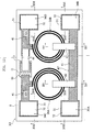
- Figs. 1 to 4 depict an integrated electronic component X1 according to a first embodiment of the present invention.
- Fig. 1 is a plan view of the integrated electronic component X1.
- Figs. 2, 3 and 4 are cross-sectional views taken along the lines II-II, III-III and IV-IV in Fig. 1, respectively.
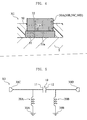
- the integrated electronic component X1 includes a substrate S, a capacitor 10, spiral coils 20A, 20B, electrode pads 30A, 30B, 30C, 30D, a wiring 40, and a protecting film 50 (not shown in Fig. 1), and has a circuit configuration shown in Fig. 5.
- the substrate S may be a semiconductor substrate, a quartz substrate, a glass substrate, a silicon on insulator (SOI) substrate, a silicon on quartz (SOQ) substrate, or a silicon on glass (SOG) substrate.
- the semiconductor substrate may be constituted of a silicon material, such as monocrystalline silicon.
- the capacitor 10 has a stacked structure including electrode films 11, 12 and a dielectric film 13 as shown in Fig. 2.
- the electrode film 11 is a lower electrode film formed in a pattern on the substrate S, and may be constituted of Cu, Au, Ag or Al.
- the electrode film 11 may have a multilayer structure including a plurality of conductor layers.
- the electrode film 11 has a thickness of 1 to 5 ⁇ m, for instance.
- the electrode film 12 is an upper electrode film having a first surface 12a facing the electrode film 11 via the dielectric film 13 and a second surface opposite to the first surface, and may be constituted of Cu, Au, Ag or Al.
- the electrode film 12 has a thickness of, for instance, 5 to 20 ⁇ m.
- the dielectric film 13 may be constituted of silicon oxide, silicon nitride, aluminum oxide, tantalum oxide or titanium oxide.
- the dielectric film 13 has a thickness of 0.1 to 0.5 ⁇ m, for instance.
- Each of the spiral coils 20A, 20B is flat spiral coils patterned on the substrate S as shown in Figs. 1 and 3, and has an inner end portion 21 (shown in Fig. 3) and an outer end portion 22 (shown in Fig. 1).
- the inner end portion 21 has a first surface 21a on the side of the substrate S and a second surface 21b opposite to the first surface 21a.
- the spiral coils 20A, 20B may have a thickness of 5 to 20 ⁇ m.
- Preferable materials of the spiral coils 20A, 20B include Cu, Au, Ag and Al.
- the electrode pads 30A to 30D serve for external connection.
- the electrode pads 30A, 30B serve as terminals for ground connection, while the electrode pads 30C, 30D serve as input/output terminals of electrical signals, as shown in Fig. 5.
- Each of the electrode pads 30A to 30D has a stacked structure including a first portion 31 and a second portion 32, as shown in Fig. 4.
- the first portion 31 has a first surface 31a on the side of the substrate S and a second surface 31b opposite to the first surface 31a, and may be constituted of Cu, Au, Ag, or Al.
- the second portion 32 may be constituted of a Ni body with the upper surface coated with a Au film.
- the wiring 40 serves to electrically connect the components on the substrate S, and includes a first wiring portion 41 patterned on the substrate S, a second wiring portion 42 patterned mainly on the protecting film 50, and a via 43 extending thicknesswise of the integrated electronic component X1, serving as a third wiring portion, as shown in Figs. 1 to 3.
- the via 43 includes a via 43A connected to the electrode film 12 of the capacitor 10, a via 43B connected to the inner end portion 21 of the spiral coils 20A, 20B, and a via 43C connecting the first wiring portion 41 and the second wiring portion 42.
- only the first wiring portion 41 out of the wiring 40 is indicated by hatching in Fig. 1.
- the first wiring portion 41 may be constituted of Cu, Au, Ag, or Al as the electrode film 11, and may have a multilayer structure including a plurality of conductor layers.
- the first wiring portion 41 has a thickness of 1 to 5 ⁇ m, for instance.
- Preferable materials of the second wiring portion 42 and the via 43 include Cu, Au, Ag, Al, and Ni, and the second wiring portion 42 may have a thickness of 5 to 20 ⁇ m.
- the via 43A has a surface 43a on the side of the substrate S, and is joined to the second surface 12b of the electrode film 12 of the capacitor 10 via the surface 43a.
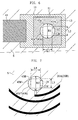
- the via 43A has, as shown in Fig. 6, a larger two-dimensional size than the electrode film 12a (Fig. 6 is an enlarged fragmentary plan view showing the capacitor 10 and the periphery thereof in the integrated electronic component X1, in which the second wiring portion 42 and the protecting film 50 are not shown but the electrode film 12 is indicated by broken lines).
- the diameter R1 of the via 43A is larger than the length L1, L2 of the electrode film 12.
- the second surface 12b of the electrode film 12 is located at an inner position of the peripheral edge 43a' of the surface 43a of the via 43A facing the substrate S.
- the surface 43a includes an extended portion 43a" extending outward of the periphery 12b' of the second surface 12b.
- the capacitor 10 is electrically connected to the electrode pads 30C, 30D and the spiral coils 20A, 20B. More specifically, as shown in Fig. 1, the electrode film 11 of the capacitor 10 is electrically connected to the electrode pad 30C and the outer end portion 22 of the spiral coil 20A via part of the first wiring portion 41, and, as shown in Figs. 1 and 2, the electrode film 12 of the capacitor 10 is electrically connected to the electrode pad 30D and the outer end portion 22 of the spiral coil 20B, via the via 43A connected to the electrode film 12, the second wiring portion 42 continuous with the via 43A, the via 43C continuous with the second wiring portion 42, and the first wiring portion 41 continuous with the via 43C.
- the via 43B has a surface 43b facing the substrate S, and is joined to the second surface 21b of the inner end portion 21 of the spiral coil 20A or the spiral coil 20B, via the surface 43b.
- the via 43B has, as shown in Fig. 7, a larger two-dimensional size than the inner end portion 21 (Fig. 7 is an enlarged fragmentary plan view showing the spiral coil 20A or the spiral coil 20B and the periphery thereof in the integrated electronic component X1, in which the second wiring portion 42 and the protecting film 50 are not shown but the inner end portion 21 is indicated by broken lines).
- Figs. 7 is an enlarged fragmentary plan view showing the spiral coil 20A or the spiral coil 20B and the periphery thereof in the integrated electronic component X1, in which the second wiring portion 42 and the protecting film 50 are not shown but the inner end portion 21 is indicated by broken lines).
- the diameter R2 of the via 43B is larger than the length L3, L4 of the inner end portion 21; and the surface 43b of the via 43B on the side of the substrate S includes an extension 43b" extending outward of the periphery 21b' of the second surface 21b of the inner end portion 21.
- the spiral coils 20A, 20B are respectively electrically connected to a part of the first wiring portion 41 on the substrate S, via the via 43B joined to the inner end portion 21, the second wiring portion 42 continuous with the via 43B, and the via 43C continuous with the second wiring portion 42.
- the spiral coils 20A, 20B are electrically connected to the electrode pads 30A, 30B, via the first wiring portion 41.
- the protecting film 50 may be constituted of a polyimide or benzocyclobutene (BCB), and covers the capacitor 10, the spiral coils 20A, 20B, the first wiring portion 41, and the via 43, as shown in Figs. 2 and 3.
- BCB benzocyclobutene
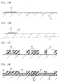
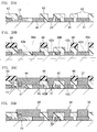
- Figs. 8A to 10D illustrate a manufacturing method of the integrated electronic component X1.
- Figs. 8A to 10D represent the progress of the formation process of the capacitor 10, a part of the spiral coil 20, an electrode pad 30 (corresponding to the electrode pads 30A to 30D), and a part of a wiring 40 shown in Fig. 10D, in cross-sectional views of a region including these constituents.
- the cross-sectional views progressively depict a model of a plurality of predetermined regions included in a single section where the integrated electronic component is formed, on a material substrate to be processed.
- the electrode film 11 of the capacitor 10 is formed on the substrate S. Specifically, a sputtering process may be performed to deposit a predetermined metal material on the substrate S, followed by a predetermined wet or dry etching process for shaping the metal film in a pattern, to form the electrode film 11.
- the dielectric film 13 is formed on the electrode film 11. Specifically, a sputtering process may be performed to deposit a predetermined dielectric material at least on the electrode film 11, followed by a predetermined wet or dry etching process for shaping the dielectric film in a pattern, to form the dielectric film 13.
- a seed layer (not shown) for electroplating is then formed on the substrate S, so as to cover the electrode film 11 and the dielectric film 13.
- the seed layer may be formed by a CVD or a sputtering process.
- a resist pattern 61 is formed.
- the resist pattern 61 has openings corresponding to the pattern shape of the electrode film 12 of the capacitor 10, the spiral coil 20, the first portion 31 of the electrode pad 30, and the first wiring portion 41 of the wiring 40.
- a liquid photoresist is firstly deposited over the substrate S from a position above the electrode film 11 and the dielectric film 13, by a spin coating process.
- the photoresist film is then patterned through an exposure and a subsequent development process.
- the resist pattern to be described later may also be formed through a similar process.
- An electroplating process is then performed to deposit a predetermined metal material in the openings of the resist pattern 61, to thereby form the electrode film 12, the spiral coil 20, the first portion 31, and the first wiring portion 41, as shown in Fig. 8D.
- the seed layer is energized.
- the resist pattern 61 is removed, for example by applying a predetermined stripping solution, followed by removal of an exposed portion of the seed layer.
- an insulating film 62 is formed so as to cover the capacitor 10, the spiral coil 20, the first portion 31, and the first wiring portion 41.
- a spin coating process may be employed to deposit a liquid photoresist on the substrate S, to form the insulating film 62.
- a resist pattern 63 is formed on the insulating film 62.
- the resist pattern 63 is formed with openings 63a, 63b, 63c corresponding to the pattern of the vias 43A, 43B, 43C, and an opening 63d corresponding to the pattern of the second portion 32 of the electrode pad 30.
- a wet etching process is then performed on the insulating film 62 utilizing the resist pattern 63 as the mask, as shown in Fig. 9D.
- the insulating film 62 becomes provided with an opening 62a for the via 43A formed such that an entirety of the second surface 12b of the electrode film 12 is exposed, an opening 62b for the via 43B formed such that an entirety of the second surface 21b of the inner end portion 21 is exposed, an opening 62c for the via 43C formed such that at least a part of an upper surface of the first wiring portion 41 in the drawing is exposed, and an opening 62d for the second portion 32 formed such that a part of the second surface 31b of the first portion 31 is exposed.
- the opening 62a does not reach the dielectric film 13 and the electrode film 11.
- the opening 62b does not reach the substrate S.
- the resist pattern 63 is removed.
- a seed layer for electroplating is then formed over the surface of the insulating film 62, and exposed surfaces of the electrode film 12, the inner end portion 21, the first portion 31, and the first wiring portion 41, after which a resist pattern 64 is formed on the insulating film 62, as shown in Fig. 10B.
- the resist pattern 64 is formed with an opening 64a corresponding to the pattern of the second wiring portion 42, and an opening 64b corresponding to the pattern of the second portion 32 of the electrode pad 30.
- an electroplating process is then performed to deposit a predetermined metal material in the openings 62a to 62d of the insulating film 62, and in the openings 64a, 64b of the resist pattern 64, to thereby form the vias 43A to 43C, the second wiring portion 42, and the second portion 32.
- the seed layer is energized.
- the via 43A does not reach the dielectric film 13 and the electrode film 11.
- the via 43B does not reach the substrate S.
- the resist pattern 64 is removed, as shown in Fig. 10D. This is followed by removal of an exposed portion of the seed layer.
- the integrated electronic component X1 shown in Fig. 1 can be manufactured.
- the process described referring to Fig. 9D allows stopping the etching process when at least a part of the second surface 31b of the first portion 31, which is to constitute a part of the electrode pad 30, as well as an entirety of the second surface 12b of the electrode film 12 of the capacitor 10 and an entirety of the second surface 21b of the inner end portion 21 of the spiral coil 20 are properly exposed, thereby preventing the opening 62a from reaching the dielectric film 13 and the electrode film 11, and the opening 62b from reaching the base material, as already stated. Accordingly, in the process described referring to Fig. 10C, the via 43A can be formed so as not to reach the dielectric film 13 and the electrode film 11, and the via 43B so as not to reach the substrate S.
- the integrated electronic component X1 therefore, higher degree of freedom is granted for designing the two-dimensional size of the electrode film 12 of the capacitor 10 in a small size, free from the restriction by the two-dimensional size or the diameter R1 (shown in Fig. 2, for example) of the via 43A to be connected to the electrode film 12, and for designing the two-dimensional size of the inner end portion 21 of the spiral coil 20 in a small size, free from the restriction by the two-dimensional size or the diameter R2 (shown in Fig. 3, for example) of the via 43B to be connected to the inner end portion 21.
- the integrated electronic component X1 thus structured facilitates reducing the static capacitance of the capacitor 10 and achieving a high Q value required from the spiral coils 20A, 20B, while satisfying the requirement for reduction in dimensions of the electronic component.
- Fig. 11 is an enlarged fragmentary plan view showing a variation of the integrated electronic component X1, corresponding to Fig. 6 taken out of Fig. 1 showing the integrated electronic component X1.
- the diameter R1 of the via 43A is larger than the length L2, but smaller than the length L1 of the electrode film 12 of the capacitor 10.
- the surface 43a of the via 43A on the side of the substrate S includes the extension 43a'' extending along an outer surface of an end portion 12b' of the second surface 12b of the electrode film 12, the second surface 12b partially extends outward from a peripheral edge 43a' of the surface 43a.
- Such configuration can also be included in the present invention, and facilitates reducing the static capacitance of the capacitor 10 while satisfying the requirement for reduction in dimensions of the electronic component.
- Fig. 12 is an enlarged fragmentary plan view showing another variation of the integrated electronic component X1, corresponding to Fig. 7 taken out of Fig. 1 showing the integrated electronic component X1.
- the diameter R2 of the via 43B is larger than the length L4, but smaller than the length L3 of the inner end portion 21 of the spiral coil 20.
- the surface 43b of the via 43B on the side of the substrate S includes the extension 43b" extending along an outer surface of an end portion 21b' of the second surface 21b of the inner end portion 21, the second surface 21b partially extends outward from a peripheral edge 43b' of the surface 43b.
- Such configuration can also be included in the present invention, and facilitates achieving a high Q value required from the spiral coils 20A, 20B, while satisfying the requirement for reduction in dimensions of the electronic component.
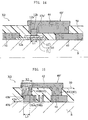
- Figs. 13 to 16 illustrate an integrated electronic component X2 according to a second embodiment of the present invention.
- Fig. 13 is a plan view showing the integrated electronic component X2.
- Figs. 14, 15, and 16 are cross-sectional views taken along the lines XIV-XIV, XV-XV, and XVI-XVI in Fig. 13, respectively.
- the integrated electronic component X2 includes a substrate S, a capacitor 10, spiral coils 20A, 20B, electrode pads 30A, 30B, 30C, 30D, a wiring 40', and a protecting film 50 (not shown in Fig. 13).
- the integrated electronic component X2 is substantially different from the foregoing integrated electronic component X1, in including the wiring 40' in place of the wiring 40.
- the wiring 40' serves to electrically connect the components on the substrate S, and includes a first wiring portion 41 patterned on the substrate S, a second wiring portion 42 patterned mainly on the protecting film 50, and a via 43 extending thicknesswise of the integrated electronic component X2, serving as a third wiring portion, as shown in Figs. 13 to 15.
- the via 43 includes a via 43B connected to the inner end portion 21 of the capacitor 10, a via 43B connected to the inner end portion 21 of the spiral coils 20A, 20B, and a via 43C connecting the first wiring portion 41 and the second wiring portion 42.
- only the first wiring portion 41 out of the wiring 40' is indicated by hatching in Fig. 13.
- the wiring 40' is different from the wiring 40 of the integrated electronic component X1, in including a fourth wiring portion 44 in place of the via 43A, the second wiring portion 42 continuous with the via 43A, and the via 43C continuous with the second wiring portion 42.
- Preferable materials of the fourth wiring portion 44 include Cu, Au, Ag, Al, and Ni, and the fourth wiring portion 44 may have a thickness of 5 to 20 ⁇ m.
- the fourth wiring portion 44 extends, as shown in Fig. 17 in addition to Fig. 14, along the substrate S and is connected to a portion of the electrode film 12 on the side of the second surface 12b, and to a part of the first wiring portion 41.
- Fig. 17 is an enlarged fragmentary plan view showing the capacitor 10 and a periphery thereof of the integrated electronic component X2, in which the protecting film 50 is not shown but the electrode film 12 is indicated by broken lines.
- the electrode film 12 of the capacitor 10 in the integrated electronic component X2 is, as shown in Fig. 13, electrically connected to the electrode pad 30D and the outer end portion 22 of the spiral coil 20B, via the fourth wiring portion 44, and the first wiring portion 41 connected to the fourth wiring portion 44.
- the electrical connections of the remaining portions of the integrated electronic component X2 are identical to those of the integrated electronic component X1.
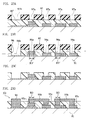
- Figs. 18A to 20D illustrate a manufacturing method of the integrated electronic component X2.
- Figs. 18A to 20D represent the progress of the formation process of the capacitor 10, a part of the spiral coil 20, the electrode pad 30 (corresponding to the electrode pads 30A to 30D), and a part of a wiring 40 shown in Fig. 20D, in cross-sectional views of a region including these constituents.
- the cross-sectional views progressively depict a model of a plurality of predetermined regions included in a single section where the integrated electronic component is formed, on a material substrate to be processed.
- the electrode film 11 of the capacitor 10 is formed on the substrate S.
- the dielectric film 13 is formed on the electrode film 11, as shown in Fig. 18B.
- a seed layer (not shown) for electroplating is then formed on the substrate S, so as to cover the electrode film 11 and the dielectric film 13, followed by formation of the resist pattern 61, as shown in Fig. 18C.
- an electroplating process is performed to form the electrode film 12, the spiral coil 20, the first portion 31, and the first wiring portion 41.
- the resist pattern 61 is removed, after which an exposed portion of the seed layer is removed. Then, as shown in Fig.
- the insulating film 62 is formed so as to cover the capacitor 10, the spiral coil 20, the first portion 31, and the first wiring portion 41. Specific details of the foregoing steps are similar to those described regarding the first embodiment, referring to Figs. 8A to 8D and 9A to 9B.
- a resist pattern 65 is formed on the insulating film 62.
- the resist pattern 65 is formed with an opening 65a corresponding to the pattern of the fourth wiring portion 44, openings 65b, 65c corresponding to the pattern of the vias 43B, 43C, and an opening 65d corresponding to the pattern of the second portion 32 of the electrode pad 30.
- a wet etching process is then performed on the insulating film 62 utilizing the resist pattern 65 as the mask, as shown in Fig. 19D.
- the insulating film 62 becomes provided with an opening 62e for the fourth wiring portion 44 formed such that an entirety of the second surface 12b of the electrode film 12 is exposed, an opening 62b for the via 43B formed such that an entirety of the second surface 21b of the inner end portion 21 is exposed, an opening 62c for the via 43C formed such that at least a part of an upper surface of the first wiring portion 41 in the drawing is exposed, and an opening 62d for the second portion 32 formed such that a part of the second surface 31b of the first portion 31 is exposed.
- the opening 62e does not reach the dielectric film 13 and the electrode film 11.
- the opening 62b does not reach the substrate S.
- the resist pattern 65 is removed, after which a seed layer (not shown) for electroplating is formed over the surface of the insulating film 62, and exposed surfaces of the electrode film 12, the inner end portion 21, the first portion 31, and the first wiring portion 41.
- a seed layer (not shown) for electroplating is formed over the surface of the insulating film 62, and exposed surfaces of the electrode film 12, the inner end portion 21, the first portion 31, and the first wiring portion 41.
- This is followed by formation of the resist pattern 66 on the insulating film 62, as shown in Fig. 20B.
- the resist pattern 66 is formed with an opening 66a corresponding to the pattern of the fourth wiring portion 44, an opening 66b corresponding to the pattern of the second wiring portion 42, and an opening 66c corresponding to the pattern of the second portion 32 of the electrode pad 30.
- an electroplating process is performed to deposit a predetermined metal material in the openings 62b to 62e of the insulating film 62 and in the openings 66a to 66c of the resist pattern 66, to thereby form the fourth wiring portion 44, the vias 43B, 43C, the second wiring portion 42, and the second portion 32.
- the seed layer is energized.
- the fourth wiring portion 44 does not reach the dielectric film 13 and the electrode film 11.
- the via 43B does not reach the substrate S.
- the resist pattern 66 is removed, as shown in Fig. 20D. This is followed by removal of an exposed portion of the seed layer.
- the integrated electronic component X2 shown in Fig. 13 can be manufactured.
- the process described referring to Fig. 19D allows stopping the etching process when at least a part of the second surface 31b of the first portion 31, which is to constitute a part of the electrode pad 30, as well as an entirety of the second surface 12b of the electrode film 12 of the capacitor 10 and an entirety of the second surface 21b of the inner end portion 21 of the spiral coil 20 are properly exposed, thereby preventing the opening 62e from reaching the dielectric film 13 and the electrode film 11, and the opening 62b from reaching the base material, as stated earlier. Accordingly, in the process described referring to Fig. 20C, the fourth wiring portion 44 can be formed so as not to reach the dielectric film 13 and the electrode film 11, and the via 43B so as not to reach the substrate S.
- the integrated electronic component X2 therefore, higher degree of freedom is granted for designing the two-dimensional size of the electrode film 12 of the capacitor 10 in a small size, free from the restriction by the shape of the fourth wiring portion 44 to be connected to the electrode film 12, and for designing the two-dimensional size of the inner end portion 21 of the spiral coil 20 in a small size, free from the restriction by the two-dimensional size or the diameter R2 (shown in Fig. 15) of the via 43B to be connected to the inner end portion 21.
- the integrated electronic component X2 thus structured facilitates reducing the static capacitance of the capacitor 10 and achieving a high Q value required from the spiral coils 20A, 20B, while satisfying the requirement for reduction in dimensions of the electronic component.
- a so-called conformal insulating film which covers the structure on the substrate S except a part of the surface of the respective electrode pads 30A to 30D, may be provided in place of the protecting film 50.
- the protecting film 50 is removed by a dry or wet etching process. Then for example a CVD process is performed to form a thin insulating film so as to cover the structure on the substrate S. The insulating film is then patterned so as to expose a part of the surfaces of the electrode pads 30A to 30D.
- Employing the conformal insulating film is advantageous in reducing parasitic capacitance that may emerge between the wirings.
Landscapes
- Engineering & Computer Science (AREA)
- Microelectronics & Electronic Packaging (AREA)
- Semiconductor Integrated Circuits (AREA)
- Internal Circuitry In Semiconductor Integrated Circuit Devices (AREA)
- Coils Or Transformers For Communication (AREA)
- Fixed Capacitors And Capacitor Manufacturing Machines (AREA)
- Parts Printed On Printed Circuit Boards (AREA)
Abstract
Description
- The present invention relates to a technique concerning an electronic component that includes a capacitor and an inductor as constituents.
- In a radio frequency (hereinafter, RF) system such as a mobile phone or a wireless LAN, signals have to be subjected to phase-matching for satisfactory transmission among functional devices constituting the system. Accordingly, the input/output terminal of each device is generally provided with a passive element that includes a passive component such as an inductor or a capacitor, and that acts as a phase shifter that controls the phase of the signals.
- There has been a constant demand for reduction in dimensions of various parts composing the RF system, driven by the increase in number of parts for achieving a higher performance. For making the system smaller in dimensions, an integrated electronic component manufactured based on a semiconductor processing technology, which includes a plurality of predetermined passive components such as an inductor, a capacitor, a resistance and a filter densely integrated on a substrate, may be employed as the passive element (phase shifter). Techniques related to the integrated electronic component are found, for example, in
JP-A-H04-61264 JP-A-2002-33239 - Fig. 21 is a fragmentary cross-sectional view showing an integrated electronic component X3 as related art for better understanding of the present invention. It should be noted that the integrated electronic component X3 was produced by the present inventors, and is not publicly known as of the priority date of the present application.
- The integrated electronic component X3 includes a
substrate 91, acapacitor 92, a spiral coil 93 (Fig. 21 shows a cross-section of a part of the lead wire thereof), anelectrode pad 94, awiring 95, and a protectingfilm 96. Thecapacitor 92 has a stacked structure includingelectrode films dielectric film 92c. Thespiral coil 93 is an inductor patterned in a flat spiral shape on thesubstrate 91, and includes aninner end portion 93a located at an innermost position of the spiral shape. Theelectrode pad 94 serves for external connection. Thewiring 95 includes afirst wiring portion 95a patterned on thesubstrate 91, asecond wiring portion 95b patterned mainly on the protectingfilm 96, and a via 95c. Theelectrode film 92a of thecapacitor 92 and theelectrode pad 94 are electrically connected directly. Avia 95c of thewiring 95 is connected to theelectrode film 92b of thecapacitor 92. Another via 95c of thewiring 95 is connected to theinner end portion 93a of thespiral coil 93. The protectingfilm 96 is disposed so as to cover thecapacitor 92 and thespiral coil 93 on thesubstrate 91. - Figs. 22A through 23D illustrate a manufacturing method of the integrated electronic component X3. To form the integrated electronic component X3, firstly the
electrode film 92a of thecapacitor 92 is patterned on thesubstrate 91, as shown in Fig. 21A. Referring to Fig. 21B, thedielectric film 92c is patterned on theelectrode film 92a. An electroplating process is then performed to form theelectrode film 92b of thecapacitor 92, the spiral coil 93 (inner end portion 93a inclusive), and thefirst wiring portion 95a of thewiring 95, as shown in Fig. 21C. This is followed by formation of an insulating film 96' on thesubstrate 91, as shown in Fig. 21D. - Proceeding to Fig. 23A, a
resist pattern 97 is formed on the insulating film 96'. Theresist pattern 97 is formed with an opening 97a corresponding to the pattern of thevia 95c of thewiring 95, and an opening 97b corresponding to the pattern of theelectrode pad 94. Then a wet etching process is performed over the insulating film 96', utilizing theresist pattern 97 as the mask, as shown in Fig. 23B. At this stage, the protectingfilm 96 provided with an opening 96a for thevia 95c and an opening 96b for theelectrode pad 94 is formed. Theresist pattern 97 is then removed, as shown in Fig. 23C. This is followed by an electroplating process for forming thevia 95c, thesecond wiring portion 95b, and theelectrode pad 94 as shown in Fig. 23D. That is how the integrated electronic component X3 is manufactured. - In the integrated electronic component X3, the protecting
film 96 is required to have a sufficient thickness (that allows securing a gap of 10 µm or wider between thespiral coil 93 and thesecond wiring portion 95b) in order to prevent undue electromagnetic interaction between thespiral coil 93 serving as the inductor and thesecond wiring portion 95b located above thespiral coil 93. The thicker the protectingfilm 96 is, the more difficult it becomes to form the opening 96a having a small diameter R3' in the process described referring to Fig. 23B, and hence to form thevia 95c of a small diameter R3. Accordingly, making the protectingfilm 96 thick causes enlarging the minimum diameter R3 (shown in Figs. 21 and 23D) which is applicable to each via 95c. In other words, the dimension of the thickness of the protectingfilm 96 determines the lower limit of the applicable diameter R3 of each via 95c. - In the integrated electronic component X3, moreover, a length L5 of the
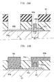
electrode film 92b of thecapacitor 92 shown in Fig. 21 cannot be made smaller than the diameter R3 of thevia 95c connected to theelectrode film 92b. Setting the length L5 of theelectrode film 92b to be smaller than the diameter R3 of thevia 95c would, in the process described referring to Fig. 23B, cause the opening 96b for theelectrode pad 94 to reach as far as theelectrode film 92a (the etching process has to be performed until the opening 96b for theelectrode pad 94 reaches theelectrode film 92a), and the opening 96a to reach thedielectric film 92c (or to even reach theelectrode film 92a, depending on the size of thedielectric film 92c), as shown in Fig. 24A. Executing the process described referring to Fig. 23D with the opening 96a thus formed would, as shown in Fig. 24B, result in formation of thevia 95c connected to thedielectric film 92c in addition to theelectrode film 92b (or even to theelectrode film 92a, depending on the size of thedielectric film 92c). Such via 95c would degrade the characteristic of thecapacitor 92, and hence the characteristic of the integrated electronic component X3. Therefore, in the integrated electronic component X3, theelectrode film 92b has to be formed with a sufficient length L5 (and a sufficient two-dimensional size) against the diameter R3 of thevia 95c connected to theelectrode film 92b. - In order to reduce the static capacitance of the
capacitor 92, while satisfying the requirement for reduction in dimensions of the integrated electronic component X3, for example the length L5 has to be set to be smaller thus to reduce the two-dimensional size of theelectrode film 92b. Actually, however, the minimum applicable diameter R3 is restrained depending on the thickness granted to the protectingfilm 96, and besides theelectrode film 92b has to be formed with a sufficient length L5 (and a sufficient two-dimensional size) against the diameter R3 of thevia 95c connected to theelectrode film 92b, as already stated. These factors impede the attempt of reducing the static capacitance of thecapacitor 92, while satisfying the requirement for reduction in dimensions of the integrated electronic component X3. - In the integrated electronic component X3, further, it is not desirable to set a length L6 of the
inner end portion 93a of thespiral coil 93 shown in Fig. 21 to be smaller than the diameter R3 of thevia 95c connected to theinner end portion 93a. Setting the length L6 of theinner end portion 93a to be smaller than the diameter R3 of thevia 95c would, in the process described referring to Fig. 23B, cause the opening 96b to reach as far as theelectrode film 92a (the etching process has to be performed until the opening 96b for theelectrode pad 94 reaches theelectrode film 92a), and the opening 96a to reach thesubstrate 91, as shown in Fig. 25A. Executing the process described referring to Fig. 23D with the opening 96a thus formed would, as shown in Fig. 25B, result in formation of thevia 95c having such a large volume as reaching thesubstrate 91. Such via 95c may incur degradation in Q value of thespiral coil 93. Therefore, in the integrated electronic component X3, theinner end portion 93a has to be formed with a sufficient length L6 (and a sufficient two-dimensional size) against the diameter R3 of thevia 95c connected to theinner end portion 93a. - In order to increase the Q value of the
spiral coil 93, while satisfying the requirement for reduction in dimensions of the integrated electronic component X3, for example the length L6 has to be set to be smaller thus to reduce the two-dimensional size of theinner end portion 93a. Actually, however, the minimum applicable diameter R3 is restrained depending on the thickness granted to the protectingfilm 96, while it is desirable to form theinner end portion 93a with a sufficient length L6 (and a sufficient two-dimensional size) against the diameter R3 of the via 95c connected to theinner end portion 93a, as already stated. These factors impede the attempt of increasing the Q value of thespiral coil 93, while satisfying the requirement for reduction in dimensions of the integrated electronic component X3. - The present invention has been proposed under the foregoing situation, to provide a method of manufacturing an electronic component appropriate for constituting an integrated electronic component, and the electronic component appropriate for constituting the integrated electronic component.
- A first aspect of the present invention provides a method of manufacturing an electronic component. The method is for manufacturing an electronic component including: a base material; an electrode pad provided on the base material, the electrode pad having a stacked structure including a first portion having a first pad-surface on the side of the base material and a second pad-surface opposite to the first pad-surface and a second portion joined to the first portion; a capacitor unit having a stacked structure including a first electrode portion provided on the base material, a second electrode portion having a first electrode-surface facing the first electrode portion and a second electrode-surface opposite to the first electrode-surface, and a dielectric portion interposed between the first and the second electrode portion; and a wiring portion including a via portion having a wiring-surface facing the base material, the wiring-surface being joined to the second electrode-surface of the second electrode portion; wherein the wiring-surface of the via portion includes an extending portion extending outward of a periphery of the second electrode-surface of the capacitor unit. The method comprises: forming an insulating film on the base material so as to cover the first portion and the capacitor unit after forming at least the first portion of the electrode pad, and the first electrode portion, the dielectric portion and the second electrode portion of the capacitor unit on the base material; and providing the insulating film with a first opening for forming the second portion such that at least part of the second pad-surface of the first portion is exposed, and with a second opening for forming the via portion such that at least part of the second electrodesurface of the second electrode portion is exposed (opening formation step). The opening formation step may include performing an etching process (for example, wet etching process) over the insulating film, through a predetermined resist pattern provided thereon.
- The opening formation step thus arranged allows stopping the etching process when at least a part of the second surface of the first portion, which is to constitute a part of the electrode pad, and at least a part of the second surface of the second electrode portion of the capacitor unit are properly exposed, thereby preventing the opening for the via portion from reaching the dielectric film and the first electrode portion. Accordingly, when performing for example an electroplating process to deposit a conductor material in the opening for the via portion after the opening formation step, thus to form the via portion connected to the second electrode portion, the via portion can be formed so as not to reach the dielectric film and the first electrode portion. In the electronic component thus manufactured, therefore, higher degree of freedom is granted for designing the two-dimensional size of the second electrode portion of the capacitor unit in a small size, free from the restriction by the two-dimensional size (or diameter) of the via portion to be connected to the second electrode portion. Such electronic component facilitates reducing the static capacitance of the capacitor unit while satisfying the requirement for reduction in dimensions of the electronic component and, consequently, is appropriate for constituting an integrated electronic component.
- A second aspect of the present invention provides a method of manufacturing an electronic component. The method of manufacturing an electronic component including: a base material; an electrode pad provided on the base material, the electrode pad having a stacked structure including a first portion having a first pad-surface on the side of the base material and a second pad-surface opposite to the first pad-surface, and a second portion joined to the first portion; a capacitor unit having a stacked structure including a first electrode portion provided on the base material, a second electrode portion having a first electrode-surface facing the first electrode portion and a second electrode-surface opposite to the first electrode-surface, and a dielectric portion interposed between the first and the second electrode portion; and a wiring portion including a joining portion extending along the base material and joined to the second electrode-surface of the second electrode portion. The method comprises: forming an insulating film on the base material so as to cover the first portion and the capacitor unit after forming at least the first portion of the electrode pad, and the first electrode portion, the dielectric portion and the second electrode portion of the capacitor unit on the base material; and providing the insulating film with a first opening for forming the second portion such that at least part of the second pad-surface of the first portion is exposed, and a second opening for forming the wiring portion such that at least part of the second electrode-surface of the second electrode portion is exposed (opening formation step). The opening formation step may include performing an etching process (for example, wet etching process) over the insulating film, through a predetermined resist pattern provided thereon.
- The opening formation step thus arranged allows stopping the etching process when at least a part of the second surface of the first portion, which is to constitute a part of the electrode pad, and at least a part of the second surface of the second electrode portion of the capacitor unit are properly exposed, thereby preventing the opening for the wiring portion from reaching the dielectric film and the first electrode portion. Accordingly, when performing for example an electroplating process to deposit a conductor material in the opening for the wiring portion after the opening formation step, thus to form the wiring portion connected to the second electrode portion, the wiring portion can be formed so as not to reach the dielectric film and the first electrode portion. In the electronic component thus manufactured, therefore, higher degree of freedom is granted for designing the two-dimensional size of the second electrode portion of the capacitor unit in a small size, free from the restriction by the shape of the wiring portion to be connected to the second electrode portion. Such electronic component facilitates reducing the static capacitance of the capacitor unit while satisfying the requirement for reduction in dimensions of the electronic component and, consequently, is appropriate for constituting an integrated electronic component.
- A third aspect of the present invention provides a method of manufacturing an electronic component. The method of manufacturing an electronic component including: a base material; an electrode pad provided on the base material, the electrode pad having a stacked structure including a first portion having a first pad-surface on the side of the base material and a second pad-surface opposite to the first pad-surface, and a second portion joined to the first portion; a spiral coil provided on the base material, the spiral coil including an inner end portion having a first coil-surface on the base material side and a second coil-surface opposite to the first coil-surface; and a wiring portion including a via portion having a wiring-surface facing the base material, the wiring-surface being joined to the second coil-surface of the inner end portion; wherein the wiring-surface of the via portion includes an extending portion extending outward of a periphery of the second coil-surface of the inner end portion. The method comprises: forming an insulating film on the base material so as to cover the first portion and the spiral coil after forming at least the first portion of the electrode pad, and the spiral coil having the inner end portion on the base material; and providing the insulating film with a first opening for forming the second portion such that at least part of the second pad-surface of the first portion is exposed, and a second opening for forming the via portion such that at least part of the second coil-surface of the inner end portion is exposed (opening formation step). The opening formation step may include performing an etching process (for example, wet etching process) over the insulating film, through a predetermined resist pattern provided thereon.
- The opening formation step thus arranged allows stopping the etching process when at least a part of the second surface of the first portion, which is to constitute a part of the electrode pad, and at least a part of the second surface of the inner end portion of the spiral coil are properly exposed, thereby preventing the opening for the via portion from reaching the base material. Accordingly, when performing for example an electroplating process to deposit a conductor material in the opening for the via portion after the opening formation step, thus to form the via portion connected to the inner end portion, the via portion can be formed so as not to reach the base material. In the electronic component thus manufactured, therefore, higher degree of freedom is granted for designing the two-dimensional size of the inner end portion of the spiral coil in a small size, free from the restriction by the two-dimensional size (or diameter) of the via portion to be connected to the inner end portion. Such electronic component facilitates achieving a high Q value required from the spiral coil while satisfying the requirement for reduction in dimensions of the electronic component and, consequently, is appropriate for constituting an integrated electronic component.
- A fourth aspect of the present invention provides an electronic component comprising a base material, a capacitor unit, and a wiring portion. The capacitor unit has a stacked structure including a first electrode portion provided on the base material, a second electrode portion having a first electrode-surface facing the first electrode portion and a second electrode-surface opposite to the first electrode-surface, and a dielectric portion interposed between the first and the second electrode portion. The wiring portion includes a via portion having a wiring-surface facing the base material, the wiring-surface being joined to the second electrode-surface of the second electrode portion. The wiring-surface includes an extending portion extending outward of a periphery of the second electrode-surface. The electronic component thus constituted may be manufactured by the method according to the first aspect of the present invention, and eliminates the restriction by the two-dimensional size (or diameter) of the via portion to be connected to the second electrode portion, when designing the two-dimensional size of the second electrode portion of the capacitor unit. Such electronic component facilitates reducing the static capacitance of the capacitor unit while satisfying the requirement for reduction in dimensions of the electronic component and, consequently, is appropriate for constituting an integrated electronic component.
- Preferably, the second electrode-surface is located at an inner position of a peripheral edge of the wiring-surface. Such configuration facilitates achieving a high Q value required from the spiral coil while satisfying the requirement for reduction in dimensions of the electronic component.
- A fifth aspect of the present invention provides an electronic component comprising a base material, a capacitor unit, and a wiring portion. The capacitor unit has a stacked structure including a first electrode portion provided on the base material, a second electrode portion having a first electrode-surface facing the first electrode portion and a second electrode-surface opposite to the first electrode-surface, and a dielectric portion interposed between the first and the second electrode portion. The wiring portion includes a joining portion extending along the base material and joined to the second electrode-surface of the second electrode portion. The electronic component thus constituted may be manufactured by the method according to the second aspect of the present invention, and eliminates the restriction by the shape of the wiring portion to be connected to the second electrode portion, when designing the two-dimensional size of the second electrode portion of the capacitor unit. Such electronic component facilitates reducing the static capacitance of the capacitor unit while satisfying the requirement for reduction in dimensions of the electronic component and, consequently, is appropriate for constituting an integrated electronic component.
- Preferably, the electronic component further comprises a passive component provided on the base material. The wiring portion constitutes at least part of an electrical path between the passive component and the capacitor unit. With or instead of such structure, the electronic component may further comprise an electrode pad provided on the base material; wherein the wiring portion constitutes at least part of an electrical path between the electrode pad and the capacitor unit.. The electronic component according to the fourth and the fifth aspect of the present invention may be an integrated electronic component including the foregoing structure.
- A sixth aspect of the present invention provides an electronic component comprising a base material, a spiral coil serving as an inductor, and a wiring portion. The spiral coil includes an inner end portion having a first coil-surface on the base material side and a second coil-surface opposite to the first coil-surface, the spiral coil being provided on the base material. The wiring portion includes a via portion having a wiring-surface facing the base material, the wiring-surface being joined to the second coil-surface of the inner end portion. The wiring-surface includes an extending portion extending outward of a periphery of the second coil-surface. The electronic component thus constituted may be manufactured by the method according to the third aspect of the present invention, and eliminates the restriction by the two-dimensional size (or diameter) of the via portion to be connected to the inner end portion, when designing the two-dimensional size of the inner end portion of the spiral coil. Such electronic component facilitates achieving a high Q value required from the spiral coil while satisfying the requirement for reduction in dimensions of the electronic component and, consequently, is appropriate for constituting an integrated electronic component.
- Preferably, the second coil-surface is located at an inner position of a peripheral edge of the wiring-surface. Such configuration facilitates reducing the static capacitance of the capacitor unit while satisfying the requirement for reduction in dimensions of the electronic component.
- Preferably, the electronic component may further comprise a passive component provided on the base material; wherein the wiring portion constitutes at least part of an electrical path between the passive component and the spiral coil. With or instead of such structure, the electronic component may further comprise an electrode pad provided on the base material; wherein the wiring portion constitutes at least part of an electrical path between the electrode pad and the spiral coil. The electronic component according to the sixth aspect of the present invention may be an integrated electronic component including the foregoing structure.
- Reference is made, by way of example only, to the accompanying drawings in which:
- Fig. 1 is a plan view showing an integrated electronic component according to a first embodiment of the present invention;
- Fig. 2 is a cross-sectional view taken along the line II-II in Fig. 1;
- Fig. 3 is a cross-sectional view taken along the line III-III in Fig. 1;
- Fig. 4 is a cross-sectional view taken along the line IV-IV in Fig. 1;
- Fig. 5 is a circuit diagram of the integrated electronic component shown in Fig. 1;
- Fig. 6 is an enlarged fragmentary plan view showing the integrated electronic component shown in Fig. 1;
- Fig. 7 is an enlarged fragmentary plan view showing another portion of the integrated electronic component shown in Fig. 1;
- Figs. 8A to 8D are cross-sectional views showing a manufacturing process of the integrated electronic component shown in Fig. 1;
- Figs. 9A to 9D are cross-sectional views showing a manufacturing process subsequent to Fig. 8D;
- Figs. 10A to 10D are cross-sectional views showing a manufacturing process subsequent to Fig. 9D;
- Fig. 11 is an enlarged fragmentary plan view showing a variation of the integrated electronic component according to the first embodiment, corresponding to Fig. 6 taken out of Fig. 1;
- Fig. 12 is an enlarged fragmentary plan view showing a variation of the integrated electronic component according to the first embodiment, corresponding to Fig. 7 taken out of Fig. 1;
- Fig. 13 is a plan view showing an integrated electronic component according to a second embodiment of the present invention;
- Fig. 14 is a cross-sectional view taken along the line XIV-XIV in Fig. 13;
- Fig. 15 is a cross-sectional view taken along the line XV-XV in Fig. 13;
- Fig. 16 is a cross-sectional view taken along the line XVI-XVI in Fig. 13;
- Fig. 17 is an enlarged fragmentary plan view showing the integrated electronic component shown in Fig. 13;
- Figs. 18A to 18D are cross-sectional views showing a manufacturing process of the integrated electronic component shown in Fig. 13;
- Figs. 19A to 19D are cross-sectional views showing a manufacturing process subsequent to Fig. 18D;
- Figs. 20A to 20D are cross-sectional views showing a manufacturing process subsequent to Fig. 19D;
- Fig. 21 is a fragmentary cross-sectional view showing an electronic component as related art for better understanding of the present invention;
- Figs. 22A to 22D are cross-sectional views showing a manufacturing process of the integrated electronic component shown in Fig. 21;
- Figs. 23A to 23D are cross-sectional views showing a manufacturing process subsequent to Fig. 22D;
- Figs. 24A and 24B are cross-sectional views showing an imaginary step in the manufacturing process of the integrated electronic component according to the related art; and
- Figs. 25A and 25B are cross-sectional views showing another imaginary step in the manufacturing process of the integrated electronic component according to the related art.
- Figs. 1 to 4 depict an integrated electronic component X1 according to a first embodiment of the present invention. Fig. 1 is a plan view of the integrated electronic component X1. Figs. 2, 3 and 4 are cross-sectional views taken along the lines II-II, III-III and IV-IV in Fig. 1, respectively.
- The integrated electronic component X1 includes a substrate S, a
capacitor 10, spiral coils 20A, 20B,electrode pads wiring 40, and a protecting film 50 (not shown in Fig. 1), and has a circuit configuration shown in Fig. 5. - The substrate S may be a semiconductor substrate, a quartz substrate, a glass substrate, a silicon on insulator (SOI) substrate, a silicon on quartz (SOQ) substrate, or a silicon on glass (SOG) substrate. The semiconductor substrate may be constituted of a silicon material, such as monocrystalline silicon.
- The
capacitor 10 has a stacked structure includingelectrode films dielectric film 13 as shown in Fig. 2. Theelectrode film 11 is a lower electrode film formed in a pattern on the substrate S, and may be constituted of Cu, Au, Ag or Al. Theelectrode film 11 may have a multilayer structure including a plurality of conductor layers. Theelectrode film 11 has a thickness of 1 to 5 µm, for instance. Theelectrode film 12 is an upper electrode film having afirst surface 12a facing theelectrode film 11 via thedielectric film 13 and a second surface opposite to the first surface, and may be constituted of Cu, Au, Ag or Al. Theelectrode film 12 has a thickness of, for instance, 5 to 20 µm. Thedielectric film 13 may be constituted of silicon oxide, silicon nitride, aluminum oxide, tantalum oxide or titanium oxide. Thedielectric film 13 has a thickness of 0.1 to 0.5 µm, for instance. - Each of the spiral coils 20A, 20B is flat spiral coils patterned on the substrate S as shown in Figs. 1 and 3, and has an inner end portion 21 (shown in Fig. 3) and an outer end portion 22 (shown in Fig. 1). The
inner end portion 21 has afirst surface 21a on the side of the substrate S and asecond surface 21b opposite to thefirst surface 21a. The spiral coils 20A, 20B may have a thickness of 5 to 20 µm. Preferable materials of the spiral coils 20A, 20B include Cu, Au, Ag and Al. - The
electrode pads 30A to 30D serve for external connection. Theelectrode pads electrode pads electrode pads 30A to 30D has a stacked structure including afirst portion 31 and asecond portion 32, as shown in Fig. 4. Thefirst portion 31 has afirst surface 31a on the side of the substrate S and asecond surface 31b opposite to thefirst surface 31a, and may be constituted of Cu, Au, Ag, or Al. Thesecond portion 32 may be constituted of a Ni body with the upper surface coated with a Au film. - The
wiring 40 serves to electrically connect the components on the substrate S, and includes afirst wiring portion 41 patterned on the substrate S, asecond wiring portion 42 patterned mainly on the protectingfilm 50, and a via 43 extending thicknesswise of the integrated electronic component X1, serving as a third wiring portion, as shown in Figs. 1 to 3. The via 43 includes a via 43A connected to theelectrode film 12 of thecapacitor 10, a via 43B connected to theinner end portion 21 of the spiral coils 20A, 20B, and a via 43C connecting thefirst wiring portion 41 and thesecond wiring portion 42. For the sake of explicitness of the drawings, only thefirst wiring portion 41 out of thewiring 40 is indicated by hatching in Fig. 1. Thefirst wiring portion 41 may be constituted of Cu, Au, Ag, or Al as theelectrode film 11, and may have a multilayer structure including a plurality of conductor layers. Thefirst wiring portion 41 has a thickness of 1 to 5 µm, for instance. Preferable materials of thesecond wiring portion 42 and the via 43 include Cu, Au, Ag, Al, and Ni, and thesecond wiring portion 42 may have a thickness of 5 to 20 µm. - As shown in Fig. 2, the via 43A has a
surface 43a on the side of the substrate S, and is joined to thesecond surface 12b of theelectrode film 12 of thecapacitor 10 via thesurface 43a. The via 43A has, as shown in Fig. 6, a larger two-dimensional size than theelectrode film 12a (Fig. 6 is an enlarged fragmentary plan view showing thecapacitor 10 and the periphery thereof in the integrated electronic component X1, in which thesecond wiring portion 42 and the protectingfilm 50 are not shown but theelectrode film 12 is indicated by broken lines). To be more detailed, as shown in Figs. 2 and 6, the diameter R1 of the via 43A is larger than the length L1, L2 of theelectrode film 12. Thesecond surface 12b of theelectrode film 12 is located at an inner position of theperipheral edge 43a' of thesurface 43a of the via 43A facing the substrate S. Thesurface 43a includes anextended portion 43a" extending outward of theperiphery 12b' of thesecond surface 12b. - Referring to Fig. 5, the
capacitor 10 is electrically connected to theelectrode pads electrode film 11 of thecapacitor 10 is electrically connected to theelectrode pad 30C and theouter end portion 22 of thespiral coil 20A via part of thefirst wiring portion 41, and, as shown in Figs. 1 and 2, theelectrode film 12 of thecapacitor 10 is electrically connected to theelectrode pad 30D and theouter end portion 22 of thespiral coil 20B, via the via 43A connected to theelectrode film 12, thesecond wiring portion 42 continuous with the via 43A, the via 43C continuous with thesecond wiring portion 42, and thefirst wiring portion 41 continuous with the via 43C. - Referring to Fig. 3, the via 43B has a
surface 43b facing the substrate S, and is joined to thesecond surface 21b of theinner end portion 21 of thespiral coil 20A or thespiral coil 20B, via thesurface 43b. The via 43B has, as shown in Fig. 7, a larger two-dimensional size than the inner end portion 21 (Fig. 7 is an enlarged fragmentary plan view showing thespiral coil 20A or thespiral coil 20B and the periphery thereof in the integrated electronic component X1, in which thesecond wiring portion 42 and the protectingfilm 50 are not shown but theinner end portion 21 is indicated by broken lines). To be more detailed, as shown in Figs. 2 and 6, the diameter R2 of the via 43B is larger than the length L3, L4 of theinner end portion 21; and thesurface 43b of the via 43B on the side of the substrate S includes anextension 43b" extending outward of theperiphery 21b' of thesecond surface 21b of theinner end portion 21. - Referring further to Fig. 3, the spiral coils 20A, 20B are respectively electrically connected to a part of the
first wiring portion 41 on the substrate S, via the via 43B joined to theinner end portion 21, thesecond wiring portion 42 continuous with the via 43B, and the via 43C continuous with thesecond wiring portion 42. Thus, the spiral coils 20A, 20B are electrically connected to theelectrode pads first wiring portion 41. - The protecting
film 50 may be constituted of a polyimide or benzocyclobutene (BCB), and covers thecapacitor 10, the spiral coils 20A, 20B, thefirst wiring portion 41, and the via 43, as shown in Figs. 2 and 3. - Figs. 8A to 10D illustrate a manufacturing method of the integrated electronic component X1. Figs. 8A to 10D represent the progress of the formation process of the
capacitor 10, a part of thespiral coil 20, an electrode pad 30 (corresponding to theelectrode pads 30A to 30D), and a part of awiring 40 shown in Fig. 10D, in cross-sectional views of a region including these constituents. The cross-sectional views progressively depict a model of a plurality of predetermined regions included in a single section where the integrated electronic component is formed, on a material substrate to be processed. - To form the integrated electronic component X1, referring first to Fig. 8A, the
electrode film 11 of thecapacitor 10 is formed on the substrate S. Specifically, a sputtering process may be performed to deposit a predetermined metal material on the substrate S, followed by a predetermined wet or dry etching process for shaping the metal film in a pattern, to form theelectrode film 11. - Then as shown in Fig. 8B, the
dielectric film 13 is formed on theelectrode film 11. Specifically, a sputtering process may be performed to deposit a predetermined dielectric material at least on theelectrode film 11, followed by a predetermined wet or dry etching process for shaping the dielectric film in a pattern, to form thedielectric film 13. - A seed layer (not shown) for electroplating is then formed on the substrate S, so as to cover the
electrode film 11 and thedielectric film 13. The seed layer may be formed by a CVD or a sputtering process. - Referring to Fig. 8C, a resist
pattern 61 is formed. The resistpattern 61 has openings corresponding to the pattern shape of theelectrode film 12 of thecapacitor 10, thespiral coil 20, thefirst portion 31 of theelectrode pad 30, and thefirst wiring portion 41 of thewiring 40. To form the resistpattern 61, a liquid photoresist is firstly deposited over the substrate S from a position above theelectrode film 11 and thedielectric film 13, by a spin coating process. The photoresist film is then patterned through an exposure and a subsequent development process. The resist pattern to be described later may also be formed through a similar process. - An electroplating process is then performed to deposit a predetermined metal material in the openings of the resist
pattern 61, to thereby form theelectrode film 12, thespiral coil 20, thefirst portion 31, and thefirst wiring portion 41, as shown in Fig. 8D. In this electroplating process, the seed layer is energized. - Proceeding to Fig. 9A, the resist
pattern 61 is removed, for example by applying a predetermined stripping solution, followed by removal of an exposed portion of the seed layer. Then as shown in Fig. 9B, an insulatingfilm 62 is formed so as to cover thecapacitor 10, thespiral coil 20, thefirst portion 31, and thefirst wiring portion 41. Specifically, a spin coating process may be employed to deposit a liquid photoresist on the substrate S, to form the insulatingfilm 62. - Referring to Fig. 9C, a resist
pattern 63 is formed on the insulatingfilm 62. The resistpattern 63 is formed withopenings opening 63d corresponding to the pattern of thesecond portion 32 of theelectrode pad 30. - A wet etching process is then performed on the insulating
film 62 utilizing the resistpattern 63 as the mask, as shown in Fig. 9D. As a result, the insulatingfilm 62 becomes provided with anopening 62a for the via 43A formed such that an entirety of thesecond surface 12b of theelectrode film 12 is exposed, anopening 62b for thevia 43B formed such that an entirety of thesecond surface 21b of theinner end portion 21 is exposed, anopening 62c for the via 43C formed such that at least a part of an upper surface of thefirst wiring portion 41 in the drawing is exposed, and anopening 62d for thesecond portion 32 formed such that a part of thesecond surface 31b of thefirst portion 31 is exposed. Theopening 62a does not reach thedielectric film 13 and theelectrode film 11. Theopening 62b does not reach the substrate S. - Proceeding to Fig. 10A, the resist
pattern 63 is removed. A seed layer for electroplating is then formed over the surface of the insulatingfilm 62, and exposed surfaces of theelectrode film 12, theinner end portion 21, thefirst portion 31, and thefirst wiring portion 41, after which a resistpattern 64 is formed on the insulatingfilm 62, as shown in Fig. 10B. The resistpattern 64 is formed with anopening 64a corresponding to the pattern of thesecond wiring portion 42, and anopening 64b corresponding to the pattern of thesecond portion 32 of theelectrode pad 30. - Referring to Fig. 10C, an electroplating process is then performed to deposit a predetermined metal material in the
openings 62a to 62d of the insulatingfilm 62, and in theopenings pattern 64, to thereby form thevias 43A to 43C, thesecond wiring portion 42, and thesecond portion 32. In this electroplating process, the seed layer is energized. The via 43A does not reach thedielectric film 13 and theelectrode film 11. The via 43B does not reach the substrate S. - Then the resist
pattern 64 is removed, as shown in Fig. 10D. This is followed by removal of an exposed portion of the seed layer. Throughout the foregoing process, the integrated electronic component X1 shown in Fig. 1 can be manufactured. - The process described referring to Fig. 9D allows stopping the etching process when at least a part of the
second surface 31b of thefirst portion 31, which is to constitute a part of theelectrode pad 30, as well as an entirety of thesecond surface 12b of theelectrode film 12 of thecapacitor 10 and an entirety of thesecond surface 21b of theinner end portion 21 of thespiral coil 20 are properly exposed, thereby preventing theopening 62a from reaching thedielectric film 13 and theelectrode film 11, and theopening 62b from reaching the base material, as already stated. Accordingly, in the process described referring to Fig. 10C, the via 43A can be formed so as not to reach thedielectric film 13 and theelectrode film 11, and thevia 43B so as not to reach the substrate S. In the integrated electronic component X1, therefore, higher degree of freedom is granted for designing the two-dimensional size of theelectrode film 12 of thecapacitor 10 in a small size, free from the restriction by the two-dimensional size or the diameter R1 (shown in Fig. 2, for example) of the via 43A to be connected to theelectrode film 12, and for designing the two-dimensional size of theinner end portion 21 of thespiral coil 20 in a small size, free from the restriction by the two-dimensional size or the diameter R2 (shown in Fig. 3, for example) of the via 43B to be connected to theinner end portion 21. The integrated electronic component X1 thus structured facilitates reducing the static capacitance of thecapacitor 10 and achieving a high Q value required from the spiral coils 20A, 20B, while satisfying the requirement for reduction in dimensions of the electronic component. - Fig. 11 is an enlarged fragmentary plan view showing a variation of the integrated electronic component X1, corresponding to Fig. 6 taken out of Fig. 1 showing the integrated electronic component X1. In this variation, the diameter R1 of the via 43A is larger than the length L2, but smaller than the length L1 of the
electrode film 12 of thecapacitor 10. In other words, although thesurface 43a of the via 43A on the side of the substrate S includes theextension 43a'' extending along an outer surface of anend portion 12b' of thesecond surface 12b of theelectrode film 12, thesecond surface 12b partially extends outward from aperipheral edge 43a' of thesurface 43a. Such configuration can also be included in the present invention, and facilitates reducing the static capacitance of thecapacitor 10 while satisfying the requirement for reduction in dimensions of the electronic component. - Fig. 12 is an enlarged fragmentary plan view showing another variation of the integrated electronic component X1, corresponding to Fig. 7 taken out of Fig. 1 showing the integrated electronic component X1. In this variation, the diameter R2 of the via 43B is larger than the length L4, but smaller than the length L3 of the
inner end portion 21 of thespiral coil 20. In other words, although thesurface 43b of the via 43B on the side of the substrate S includes theextension 43b" extending along an outer surface of anend portion 21b' of thesecond surface 21b of theinner end portion 21, thesecond surface 21b partially extends outward from aperipheral edge 43b' of thesurface 43b. Such configuration can also be included in the present invention, and facilitates achieving a high Q value required from the spiral coils 20A, 20B, while satisfying the requirement for reduction in dimensions of the electronic component. - Figs. 13 to 16 illustrate an integrated electronic component X2 according to a second embodiment of the present invention. Fig. 13 is a plan view showing the integrated electronic component X2. Figs. 14, 15, and 16 are cross-sectional views taken along the lines XIV-XIV, XV-XV, and XVI-XVI in Fig. 13, respectively. The integrated electronic component X2 includes a substrate S, a
capacitor 10, spiral coils 20A, 20B,electrode pads wiring 40. - The wiring 40' serves to electrically connect the components on the substrate S, and includes a
first wiring portion 41 patterned on the substrate S, asecond wiring portion 42 patterned mainly on the protectingfilm 50, and a via 43 extending thicknesswise of the integrated electronic component X2, serving as a third wiring portion, as shown in Figs. 13 to 15. The via 43 includes a via 43B connected to theinner end portion 21 of thecapacitor 10, a via 43B connected to theinner end portion 21 of the spiral coils 20A, 20B, and a via 43C connecting thefirst wiring portion 41 and thesecond wiring portion 42. For the sake of explicitness of the drawings, only thefirst wiring portion 41 out of the wiring 40' is indicated by hatching in Fig. 13. The wiring 40' is different from thewiring 40 of the integrated electronic component X1, in including afourth wiring portion 44 in place of the via 43A, thesecond wiring portion 42 continuous with the via 43A, and the via 43C continuous with thesecond wiring portion 42. Preferable materials of thefourth wiring portion 44 include Cu, Au, Ag, Al, and Ni, and thefourth wiring portion 44 may have a thickness of 5 to 20 µm. - The
fourth wiring portion 44 extends, as shown in Fig. 17 in addition to Fig. 14, along the substrate S and is connected to a portion of theelectrode film 12 on the side of thesecond surface 12b, and to a part of thefirst wiring portion 41. Fig. 17 is an enlarged fragmentary plan view showing thecapacitor 10 and a periphery thereof of the integrated electronic component X2, in which the protectingfilm 50 is not shown but theelectrode film 12 is indicated by broken lines. Theelectrode film 12 of thecapacitor 10 in the integrated electronic component X2 is, as shown in Fig. 13, electrically connected to theelectrode pad 30D and theouter end portion 22 of thespiral coil 20B, via thefourth wiring portion 44, and thefirst wiring portion 41 connected to thefourth wiring portion 44. The electrical connections of the remaining portions of the integrated electronic component X2 are identical to those of the integrated electronic component X1. - Figs. 18A to 20D illustrate a manufacturing method of the integrated electronic component X2. Figs. 18A to 20D represent the progress of the formation process of the
capacitor 10, a part of thespiral coil 20, the electrode pad 30 (corresponding to theelectrode pads 30A to 30D), and a part of awiring 40 shown in Fig. 20D, in cross-sectional views of a region including these constituents. The cross-sectional views progressively depict a model of a plurality of predetermined regions included in a single section where the integrated electronic component is formed, on a material substrate to be processed. - To form the integrated electronic component X2, referring first to Fig. 18A, the
electrode film 11 of thecapacitor 10 is formed on the substrate S. Then thedielectric film 13 is formed on theelectrode film 11, as shown in Fig. 18B. A seed layer (not shown) for electroplating is then formed on the substrate S, so as to cover theelectrode film 11 and thedielectric film 13, followed by formation of the resistpattern 61, as shown in Fig. 18C. Referring to Fig. 18D, an electroplating process is performed to form theelectrode film 12, thespiral coil 20, thefirst portion 31, and thefirst wiring portion 41. Proceeding to Fig. 19A, the resistpattern 61 is removed, after which an exposed portion of the seed layer is removed. Then, as shown in Fig. 19B, the insulatingfilm 62 is formed so as to cover thecapacitor 10, thespiral coil 20, thefirst portion 31, and thefirst wiring portion 41. Specific details of the foregoing steps are similar to those described regarding the first embodiment, referring to Figs. 8A to 8D and 9A to 9B. - The manufacturing process of the integrated electronic component X2 now proceeds to Fig. 19C, in which a resist
pattern 65 is formed on the insulatingfilm 62. The resistpattern 65 is formed with anopening 65a corresponding to the pattern of thefourth wiring portion 44,openings opening 65d corresponding to the pattern of thesecond portion 32 of theelectrode pad 30. - A wet etching process is then performed on the insulating
film 62 utilizing the resistpattern 65 as the mask, as shown in Fig. 19D. As a result, the insulatingfilm 62 becomes provided with anopening 62e for thefourth wiring portion 44 formed such that an entirety of thesecond surface 12b of theelectrode film 12 is exposed, anopening 62b for thevia 43B formed such that an entirety of thesecond surface 21b of theinner end portion 21 is exposed, anopening 62c for the via 43C formed such that at least a part of an upper surface of thefirst wiring portion 41 in the drawing is exposed, and anopening 62d for thesecond portion 32 formed such that a part of thesecond surface 31b of thefirst portion 31 is exposed. Theopening 62e does not reach thedielectric film 13 and theelectrode film 11. Theopening 62b does not reach the substrate S. - Proceeding t o Fig. 20A, the resist
pattern 65 is removed, after which a seed layer (not shown) for electroplating is formed over the surface of the insulatingfilm 62, and exposed surfaces of theelectrode film 12, theinner end portion 21, thefirst portion 31, and thefirst wiring portion 41. This is followed by formation of the resistpattern 66 on the insulatingfilm 62, as shown in Fig. 20B. The resistpattern 66 is formed with anopening 66a corresponding to the pattern of thefourth wiring portion 44, anopening 66b corresponding to the pattern of thesecond wiring portion 42, and anopening 66c corresponding to the pattern of thesecond portion 32 of theelectrode pad 30. - Then referring to Fig. 20C, an electroplating process is performed to deposit a predetermined metal material in the
openings 62b to 62e of the insulatingfilm 62 and in theopenings 66a to 66c of the resistpattern 66, to thereby form thefourth wiring portion 44, thevias second wiring portion 42, and thesecond portion 32. In this electroplating process, the seed layer is energized. Thefourth wiring portion 44 does not reach thedielectric film 13 and theelectrode film 11. The via 43B does not reach the substrate S. - Then the resist
pattern 66 is removed, as shown in Fig. 20D. This is followed by removal of an exposed portion of the seed layer. Throughout the foregoing process, the integrated electronic component X2 shown in Fig. 13 can be manufactured. - The process described referring to Fig. 19D allows stopping the etching process when at least a part of the
second surface 31b of thefirst portion 31, which is to constitute a part of theelectrode pad 30, as well as an entirety of thesecond surface 12b of theelectrode film 12 of thecapacitor 10 and an entirety of thesecond surface 21b of theinner end portion 21 of thespiral coil 20 are properly exposed, thereby preventing theopening 62e from reaching thedielectric film 13 and theelectrode film 11, and theopening 62b from reaching the base material, as stated earlier. Accordingly, in the process described referring to Fig. 20C, thefourth wiring portion 44 can be formed so as not to reach thedielectric film 13 and theelectrode film 11, and thevia 43B so as not to reach the substrate S. In the integrated electronic component X2, therefore, higher degree of freedom is granted for designing the two-dimensional size of theelectrode film 12 of thecapacitor 10 in a small size, free from the restriction by the shape of thefourth wiring portion 44 to be connected to theelectrode film 12, and for designing the two-dimensional size of theinner end portion 21 of thespiral coil 20 in a small size, free from the restriction by the two-dimensional size or the diameter R2 (shown in Fig. 15) of the via 43B to be connected to theinner end portion 21. The integrated electronic component X2 thus structured facilitates reducing the static capacitance of thecapacitor 10 and achieving a high Q value required from the spiral coils 20A, 20B, while satisfying the requirement for reduction in dimensions of the electronic component. - In the integrated electronic components X1, X2, a so-called conformal insulating film, which covers the structure on the substrate S except a part of the surface of the
respective electrode pads 30A to 30D, may be provided in place of the protectingfilm 50. To form such conformal insulating film in the integrated electronic components X1, X2, firstly the protectingfilm 50 is removed by a dry or wet etching process. Then for example a CVD process is performed to form a thin insulating film so as to cover the structure on the substrate S. The insulating film is then patterned so as to expose a part of the surfaces of theelectrode pads 30A to 30D. Employing the conformal insulating film is advantageous in reducing parasitic capacitance that may emerge between the wirings.
Claims (12)
- A method of manufacturing an electronic component including:a base material;an electrode pad provided on the base material, the electrode pad having a stacked structure including a first portion having a first pad-surface on the side of the base material and a second pad-surface opposite to the first pad-surface and a second portion joined to the first portion;a capacitor unit having a stacked structure including a first electrode portion provided on the base material, a second electrode portion having a first electrode-surface facing the first electrode portion and a second electrode surface opposite to the first electrode-surface, and a dielectric portion interposed between the first and the second electrode portion; anda wiring portion including a via portion having a wiring-surface facing the base material, the wiring-surface being joined to the second electrode-surface of the second electrode portion;wherein the wiring-surface of the via portion includes an extending portion extending outward of a periphery of the second electrode-surface of the capacitor unit,
the method comprising:forming an insulating film on the base material so as to cover the first portion and the capacitor unit after forming at least the first portion of the electrode pad, and the first electrode portion, the dielectric portion and the second electrode portion of the capacitor unit on the base material; andproviding the insulating film with a first opening for forming the second portion such that at least part of the second pad-surface of the first portion is exposed, and with a second opening for forming the via portion such that at least part of the second electrode-surface of the second electrode portion is exposed. - A method of manufacturing an electronic component including:a base material;an electrode pad provided on the base material, the electrode pad having a stacked structure including a first portion having a first pad-surface on the side of the base material and a second pad-surface opposite to the first pad-surface, and a second portion joined to the first portion;a capacitor unit having a stacked structure including a first electrode portion provided on the base material, a second electrode portion having a first electrode-surface facing the first electrode portion and a second electrode-surface opposite to the first electrode-surface, and a dielectric portion interposed between the first and the second electrode portion; anda wiring portion including a joining portion extending along the base material and joined to the second electrode-surface of the second electrode portion,the method comprising:forming an insulating film on the base material so as to cover the first portion and the capacitor unit after forming at least the first portion of the electrode pad, and the first electrode portion, the dielectric portion and the second electrode portion of the capacitor unit on the base material; andproviding the insulating film with a first opening for forming the second portion such that at least part of the second pad-surface of the first portion is exposed, and a second opening for forming the wiring portion such that at least part of the second electrode-surface of the second electrode portion is exposed.
- A method of manufacturing an electronic component including:a base material;an electrode pad provided on the base material, the electrode pad having a stacked structure including a first portion having a first pad-surface on the side of the base material and a second pad-surface opposite to the first pad-surface, and a second portion joined to the first portion;a spiral coil provided on the base material, the spiral coil including an inner end portion having a first coil-surface on the base material side and a second coil-surface opposite to the first coil-surface; anda wiring portion including a via portion having a wiring-surface facing the base material, the wiring-surface being joined to the second coil-surface of the inner end portion;wherein the wiring-surface of the via portion includes an extending portion extending outward of a periphery of the second coil-surface of the inner end portion,
the method comprising:forming an insulating film on the base material so as to cover the first portion and the spiral coil after forming at least the first portion of the electrode pad, and the spiral coil having the inner end portion on the base material; andproviding the insulating film with a first opening for forming the second portion such that at least part of the second pad-surface of the first portion is exposed, and a second opening for forming the via portion such that at least part of the second coil-surface of the inner end portion is exposed. - An electronic component comprising:a base material;a capacitor unit having a stacked structure including a first electrode portion provided on the base material, a second electrode portion having a first electrode-surface facing the first electrode portion and a second electrode-surface opposite to the first electrode-surface, and a dielectric portion interposed between the first and the second electrode portion; anda wiring portion including a via portion having a wiring-surface facing the base material, the wiring-surface being joined to the second electrode-surface of the second electrode portion;wherein the wiring-surface includes an extending portion extending outward of a periphery of the second electrode-surface.
- The electronic component according to claim 4, wherein the second electrode-surface is located at an inner position of a peripheral edge of the wiring-surface.
- An electronic component comprising:a base material;a capacitor unit having a stacked structure including a first electrode portion provided on the base material, a second electrode portion having a first electrode-surface facing the first electrode portion and a second electrode-surface opposite to the first electrode-surface, and a dielectric portion interposed between the first and the second electrode portion; anda wiring portion including a joining portion extending along the base material and joined to the second electrode-surface of the second electrode portion.
- The electronic component according to any one of claims 4 and 6, further comprising a passive component provided on the base material; wherein the wiring portion constitutes at least part of an electrical path between the passive component and the capacitor unit.
- The electronic component according to any one of claims 4 and 6, further comprising an electrode pad provided on the base material; wherein the wiring portion constitutes at least part of an electrical path between the electrode pad and the capacitor unit.
- An electronic component comprising:a base material;a spiral coil including an inner end portion having a first coil-surface on the base material side and a second coil-surface opposite to the first coil-surface, the spiral coil being provided on the base material; anda wiring portion including a via portion having a wiring-surface facing the base material, the wiring-surface being joined to the second coil-surface of the inner end portion;wherein the wiring-surface includes an extending portion extending outward of a periphery of the second coil-surface.
- The electronic component according to claim 9, wherein the second coil-surface is located at an inner position of a peripheral edge of the wiring-surface.
- The electronic component according to claim 9, further comprising a passive component provided on the base material; wherein the wiring portion constitutes at least part of an electrical path between the passive component and the spiral coil.
- The electronic component according to claim 9, further comprising an electrode pad provided on the base material; wherein the wiring portion constitutes at least part of an electrical path between the electrode pad and the spiral coil.
Applications Claiming Priority (1)
| Application Number | Priority Date | Filing Date | Title |
|---|---|---|---|
| JP2005340121A JP2007149827A (en) | 2005-11-25 | 2005-11-25 | Electronic component manufacturing method and electronic component |
Publications (2)
| Publication Number | Publication Date |
|---|---|
| EP1791404A1 true EP1791404A1 (en) | 2007-05-30 |
| EP1791404B1 EP1791404B1 (en) | 2011-02-23 |
Family
ID=37649522
Family Applications (1)
| Application Number | Title | Priority Date | Filing Date |
|---|---|---|---|
| EP06255448A Not-in-force EP1791404B1 (en) | 2005-11-25 | 2006-10-23 | Electronic component and manufacturing method thereof |
Country Status (6)
| Country | Link |
|---|---|
| US (1) | US7808030B2 (en) |
| EP (1) | EP1791404B1 (en) |
| JP (1) | JP2007149827A (en) |
| KR (1) | KR100763740B1 (en) |
| CN (1) | CN100472754C (en) |
| DE (1) | DE602006020226D1 (en) |
Cited By (1)
| Publication number | Priority date | Publication date | Assignee | Title |
|---|---|---|---|---|
| EP3720258A4 (en) * | 2017-11-30 | 2020-12-30 | Toppan Printing Co., Ltd. | GLASS CORE, MULTI-LAYER WIRING SUBSTRATE AND METHOD FOR MANUFACTURING A GLASS CORE |
Families Citing this family (17)
| Publication number | Priority date | Publication date | Assignee | Title |
|---|---|---|---|---|
| US7814112B2 (en) * | 2006-06-09 | 2010-10-12 | Ebay Inc. | Determining relevancy and desirability of terms |
| US7544580B2 (en) * | 2006-12-22 | 2009-06-09 | United Microelectronics Corp. | Method for manufacturing passive components |
| JP5133047B2 (en) * | 2007-12-28 | 2013-01-30 | 太陽誘電株式会社 | Manufacturing method of electronic parts |
| US20130271251A1 (en) * | 2012-04-12 | 2013-10-17 | Cyntec Co., Ltd. | Substrate-Less Electronic Component |
| JP5737313B2 (en) * | 2013-03-28 | 2015-06-17 | Tdk株式会社 | Electronic component and manufacturing method thereof |
| US9893048B2 (en) * | 2015-09-14 | 2018-02-13 | Qualcomm Incorporated | Passive-on-glass (POG) device and method |
| KR102521554B1 (en) * | 2015-12-07 | 2023-04-13 | 삼성전자주식회사 | Wiring structure, method of designing a wiring structure, and method of forming a wiring structure |
| US10297494B2 (en) * | 2017-01-26 | 2019-05-21 | Taiwan Semiconductor Manufacturing Company, Ltd. | Raised via for terminal connections on different planes |
| DE102017127920A1 (en) | 2017-01-26 | 2018-07-26 | Taiwan Semiconductor Manufacturing Company, Ltd. | Increased through-hole for connections on different levels |
| US10622302B2 (en) | 2018-02-14 | 2020-04-14 | Taiwan Semiconductor Manufacturing Company, Ltd. | Via for semiconductor device connection and methods of forming the same |
| US11158775B2 (en) | 2018-06-08 | 2021-10-26 | Taiwan Semiconductor Manufacturing Company, Ltd. | Semiconductor device and method |
| DE102018126130B4 (en) | 2018-06-08 | 2023-08-10 | Taiwan Semiconductor Manufacturing Co., Ltd. | semiconductor device and method |
| US10992100B2 (en) | 2018-07-06 | 2021-04-27 | Taiwan Semiconductor Manufacturing Company, Ltd. | Semiconductor device and method |
| JP7266996B2 (en) | 2018-11-20 | 2023-05-01 | 太陽誘電株式会社 | Inductors, filters and multiplexers |
| JP6546711B1 (en) * | 2019-04-10 | 2019-07-17 | 株式会社エスケーエレクトロニクス | Non-contact information carrier |
| CN111243852B (en) * | 2020-03-05 | 2021-07-30 | 上海迈铸半导体科技有限公司 | Method for reducing tail length tolerance of spiral coil, spiral coil and spiral inductor |
| JP7758341B2 (en) * | 2022-03-07 | 2025-10-22 | 住友電工デバイス・イノベーション株式会社 | Capacitor and manufacturing method thereof |
Citations (4)
| Publication number | Priority date | Publication date | Assignee | Title |
|---|---|---|---|---|
| JP2002033239A (en) * | 2000-07-14 | 2002-01-31 | Hitachi Ltd | LC filter |
| US20030201484A1 (en) * | 2002-04-26 | 2003-10-30 | Nec Electronics Corporation | Semiconductor capacitive element, method for manufacturing same and semiconductor device provided with same |
| US20030219956A1 (en) * | 2002-05-27 | 2003-11-27 | Nec Corporation | Thin film capacitor, method for manufacturing the same and printed circuit board incorporating the same |
| US20040080021A1 (en) * | 2001-09-21 | 2004-04-29 | Casper Michael D. | Integrated thin film capacitor/inductor/interconnect system and method |
Family Cites Families (13)
| Publication number | Priority date | Publication date | Assignee | Title |
|---|---|---|---|---|
| JPH0384953A (en) * | 1989-08-28 | 1991-04-10 | Seiko Epson Corp | Semiconductor integrated circuit device |
| JP2926790B2 (en) * | 1989-10-26 | 1999-07-28 | 日本電気株式会社 | Semiconductor device |
| JPH0461264A (en) | 1990-06-29 | 1992-02-27 | Nippon Telegr & Teleph Corp <Ntt> | Ic composite device |
| JPH06125011A (en) * | 1992-10-09 | 1994-05-06 | Mitsubishi Electric Corp | Semiconductor device and manufacturing method thereof |
| JP3208119B2 (en) | 1994-03-10 | 2001-09-10 | 松下電器産業株式会社 | High frequency semiconductor device |
| KR100268424B1 (en) | 1998-08-07 | 2000-10-16 | 윤종용 | A method of fabricating interconnect of semiconductor device |
| JP4256575B2 (en) | 2000-08-15 | 2009-04-22 | パナソニック株式会社 | RF passive circuit and RF amplifier with via hole |
| JP4226804B2 (en) | 2001-06-25 | 2009-02-18 | 株式会社東芝 | Semiconductor device and manufacturing method thereof |
| JP3882779B2 (en) * | 2002-05-27 | 2007-02-21 | 日本電気株式会社 | Thin film capacitor, composite passive component including thin film capacitor, method for manufacturing the same, and wiring board incorporating them |
| JP3944455B2 (en) * | 2003-01-31 | 2007-07-11 | 松下電器産業株式会社 | Semiconductor device and manufacturing method thereof |
| JP2004273920A (en) | 2003-03-11 | 2004-09-30 | Toshiba Corp | Semiconductor device |
| JP4016340B2 (en) * | 2003-06-13 | 2007-12-05 | ソニー株式会社 | Semiconductor device, mounting structure thereof, and manufacturing method thereof |
| JP4762531B2 (en) | 2004-11-30 | 2011-08-31 | 太陽誘電株式会社 | Electronic component and manufacturing method thereof |
-
2005
- 2005-11-25 JP JP2005340121A patent/JP2007149827A/en active Pending
-
2006
- 2006-10-23 DE DE602006020226T patent/DE602006020226D1/en active Active
- 2006-10-23 EP EP06255448A patent/EP1791404B1/en not_active Not-in-force
- 2006-10-30 KR KR1020060105783A patent/KR100763740B1/en not_active Expired - Fee Related
- 2006-11-13 US US11/595,913 patent/US7808030B2/en not_active Expired - Fee Related
- 2006-11-16 CN CNB2006101485560A patent/CN100472754C/en not_active Expired - Fee Related
Patent Citations (4)
| Publication number | Priority date | Publication date | Assignee | Title |
|---|---|---|---|---|
| JP2002033239A (en) * | 2000-07-14 | 2002-01-31 | Hitachi Ltd | LC filter |
| US20040080021A1 (en) * | 2001-09-21 | 2004-04-29 | Casper Michael D. | Integrated thin film capacitor/inductor/interconnect system and method |
| US20030201484A1 (en) * | 2002-04-26 | 2003-10-30 | Nec Electronics Corporation | Semiconductor capacitive element, method for manufacturing same and semiconductor device provided with same |
| US20030219956A1 (en) * | 2002-05-27 | 2003-11-27 | Nec Corporation | Thin film capacitor, method for manufacturing the same and printed circuit board incorporating the same |
Cited By (1)
| Publication number | Priority date | Publication date | Assignee | Title |
|---|---|---|---|---|
| EP3720258A4 (en) * | 2017-11-30 | 2020-12-30 | Toppan Printing Co., Ltd. | GLASS CORE, MULTI-LAYER WIRING SUBSTRATE AND METHOD FOR MANUFACTURING A GLASS CORE |
Also Published As
| Publication number | Publication date |
|---|---|
| KR100763740B1 (en) | 2007-10-04 |
| US7808030B2 (en) | 2010-10-05 |
| EP1791404B1 (en) | 2011-02-23 |
| DE602006020226D1 (en) | 2011-04-07 |
| US20070122992A1 (en) | 2007-05-31 |
| JP2007149827A (en) | 2007-06-14 |
| CN1971877A (en) | 2007-05-30 |
| CN100472754C (en) | 2009-03-25 |
| KR20070055332A (en) | 2007-05-30 |
Similar Documents
| Publication | Publication Date | Title |
|---|---|---|
| EP1791404B1 (en) | Electronic component and manufacturing method thereof | |
| CN100592440C (en) | Coil parts and manufacturing method thereof | |
| US5788854A (en) | Methods for fabrication of thin film inductors, inductor networks, inductor/capactor filters, and integration with other passive and active devices, and the resultant devices | |
| US6249039B1 (en) | Integrated inductive components and method of fabricating such components | |
| KR101040430B1 (en) | Electronic parts | |
| EP1075004A1 (en) | Capacitor | |
| JP2000277693A (en) | Integrated circuit incorporating inductive elements and method of manufacturing such an integrated circuit | |
| JP2002542619A (en) | Ultra-small resistor-capacitor thin-film network for inverted surface mounting | |
| JP2019186518A (en) | Coil component and manufacturing method of the same | |
| JP2003273684A (en) | Element having inductor and capacitor and method for manufacturing the same | |
| JP2982193B2 (en) | Manufacturing method of high frequency coil | |
| CN110349927B (en) | Multilayer wiring structure and method of manufacturing the same | |
| KR100766213B1 (en) | Electronic component | |
| CN110098054B (en) | Capacitor assembly | |
| US6781229B1 (en) | Method for integrating passives on-die utilizing under bump metal and related structure | |
| US7473981B2 (en) | Electronic component | |
| JP3559468B2 (en) | Manufacturing method of thin film wiring board | |
| JP2002280219A (en) | Inductor and / or circuit wiring near the inductor and method for manufacturing the same | |
| US20250008662A1 (en) | Functional substrate and method for manufacturing the same, and electronic device | |
| WO2004093105A1 (en) | Method of forming sheet having foreign material portions used for forming multilayer wiring board and sheet having foreign portions | |
| JP2005310841A (en) | Circuit module body and manufacturing method thereof | |
| JPH09205044A (en) | Manufacturing method of chip parts | |
| JP2002217372A (en) | Method for manufacturing semiconductor device |
Legal Events
| Date | Code | Title | Description |
|---|---|---|---|
| PUAI | Public reference made under article 153(3) epc to a published international application that has entered the european phase |
Free format text: ORIGINAL CODE: 0009012 |
|
| AK | Designated contracting states |
Kind code of ref document: A1 Designated state(s): AT BE BG CH CY CZ DE DK EE ES FI FR GB GR HU IE IS IT LI LT LU LV MC NL PL PT RO SE SI SK TR |
|
| AX | Request for extension of the european patent |
Extension state: AL BA HR MK YU |
|
| 17P | Request for examination filed |
Effective date: 20071126 |
|
| AKX | Designation fees paid |
Designated state(s): DE FR GB |
|
| GRAP | Despatch of communication of intention to grant a patent |
Free format text: ORIGINAL CODE: EPIDOSNIGR1 |
|
| RIN1 | Information on inventor provided before grant (corrected) |
Inventor name: UEDA, SATOSHI Inventor name: MATSUMOTO, TSUYOSHI Inventor name: OKUDA, HISAO Inventor name: MI, XIAOYU Inventor name: MIZUNO, YOSHIHIRO |
|
| GRAS | Grant fee paid |
Free format text: ORIGINAL CODE: EPIDOSNIGR3 |
|
| GRAA | (expected) grant |
Free format text: ORIGINAL CODE: 0009210 |
|
| AK | Designated contracting states |
Kind code of ref document: B1 Designated state(s): DE FR GB |
|
| REG | Reference to a national code |
Ref country code: GB Ref legal event code: FG4D |
|
| REF | Corresponds to: |
Ref document number: 602006020226 Country of ref document: DE Date of ref document: 20110407 Kind code of ref document: P |
|
| REG | Reference to a national code |
Ref country code: DE Ref legal event code: R096 Ref document number: 602006020226 Country of ref document: DE Effective date: 20110407 |
|
| PLBE | No opposition filed within time limit |
Free format text: ORIGINAL CODE: 0009261 |
|
| STAA | Information on the status of an ep patent application or granted ep patent |
Free format text: STATUS: NO OPPOSITION FILED WITHIN TIME LIMIT |
|
| 26N | No opposition filed |
Effective date: 20111124 |
|
| REG | Reference to a national code |
Ref country code: DE Ref legal event code: R097 Ref document number: 602006020226 Country of ref document: DE Effective date: 20111124 |
|
| PGFP | Annual fee paid to national office [announced via postgrant information from national office to epo] |
Ref country code: DE Payment date: 20121017 Year of fee payment: 7 Ref country code: FR Payment date: 20121018 Year of fee payment: 7 |
|
| PGFP | Annual fee paid to national office [announced via postgrant information from national office to epo] |
Ref country code: GB Payment date: 20121017 Year of fee payment: 7 |
|
| GBPC | Gb: european patent ceased through non-payment of renewal fee |
Effective date: 20131023 |
|
| REG | Reference to a national code |
Ref country code: DE Ref legal event code: R119 Ref document number: 602006020226 Country of ref document: DE Effective date: 20140501 |
|
| PG25 | Lapsed in a contracting state [announced via postgrant information from national office to epo] |
Ref country code: GB Free format text: LAPSE BECAUSE OF NON-PAYMENT OF DUE FEES Effective date: 20131023 |
|
| REG | Reference to a national code |
Ref country code: FR Ref legal event code: ST Effective date: 20140630 |
|
| PG25 | Lapsed in a contracting state [announced via postgrant information from national office to epo] |
Ref country code: DE Free format text: LAPSE BECAUSE OF NON-PAYMENT OF DUE FEES Effective date: 20140501 Ref country code: FR Free format text: LAPSE BECAUSE OF NON-PAYMENT OF DUE FEES Effective date: 20131031 |