EP1785977B1 - Plasma display apparatus - Google Patents
Plasma display apparatus Download PDFInfo
- Publication number
- EP1785977B1 EP1785977B1 EP06250085A EP06250085A EP1785977B1 EP 1785977 B1 EP1785977 B1 EP 1785977B1 EP 06250085 A EP06250085 A EP 06250085A EP 06250085 A EP06250085 A EP 06250085A EP 1785977 B1 EP1785977 B1 EP 1785977B1
- Authority
- EP
- European Patent Office
- Prior art keywords
- sustain
- plasma display
- waveform
- display apparatus
- scan
- Prior art date
- Legal status (The legal status is an assumption and is not a legal conclusion. Google has not performed a legal analysis and makes no representation as to the accuracy of the status listed.)
- Expired - Fee Related
Links
Images


Classifications
-
- G—PHYSICS
- G09—EDUCATION; CRYPTOGRAPHY; DISPLAY; ADVERTISING; SEALS
- G09G—ARRANGEMENTS OR CIRCUITS FOR CONTROL OF INDICATING DEVICES USING STATIC MEANS TO PRESENT VARIABLE INFORMATION
- G09G3/00—Control arrangements or circuits, of interest only in connection with visual indicators other than cathode-ray tubes
- G09G3/20—Control arrangements or circuits, of interest only in connection with visual indicators other than cathode-ray tubes for presentation of an assembly of a number of characters, e.g. a page, by composing the assembly by combination of individual elements arranged in a matrix no fixed position being assigned to or needed to be assigned to the individual characters or partial characters
- G09G3/22—Control arrangements or circuits, of interest only in connection with visual indicators other than cathode-ray tubes for presentation of an assembly of a number of characters, e.g. a page, by composing the assembly by combination of individual elements arranged in a matrix no fixed position being assigned to or needed to be assigned to the individual characters or partial characters using controlled light sources
- G09G3/28—Control arrangements or circuits, of interest only in connection with visual indicators other than cathode-ray tubes for presentation of an assembly of a number of characters, e.g. a page, by composing the assembly by combination of individual elements arranged in a matrix no fixed position being assigned to or needed to be assigned to the individual characters or partial characters using controlled light sources using luminous gas-discharge panels, e.g. plasma panels
- G09G3/288—Control arrangements or circuits, of interest only in connection with visual indicators other than cathode-ray tubes for presentation of an assembly of a number of characters, e.g. a page, by composing the assembly by combination of individual elements arranged in a matrix no fixed position being assigned to or needed to be assigned to the individual characters or partial characters using controlled light sources using luminous gas-discharge panels, e.g. plasma panels using AC panels
- G09G3/296—Driving circuits for producing the waveforms applied to the driving electrodes
-
- G—PHYSICS
- G09—EDUCATION; CRYPTOGRAPHY; DISPLAY; ADVERTISING; SEALS
- G09G—ARRANGEMENTS OR CIRCUITS FOR CONTROL OF INDICATING DEVICES USING STATIC MEANS TO PRESENT VARIABLE INFORMATION
- G09G3/00—Control arrangements or circuits, of interest only in connection with visual indicators other than cathode-ray tubes
- G09G3/20—Control arrangements or circuits, of interest only in connection with visual indicators other than cathode-ray tubes for presentation of an assembly of a number of characters, e.g. a page, by composing the assembly by combination of individual elements arranged in a matrix no fixed position being assigned to or needed to be assigned to the individual characters or partial characters
- G09G3/22—Control arrangements or circuits, of interest only in connection with visual indicators other than cathode-ray tubes for presentation of an assembly of a number of characters, e.g. a page, by composing the assembly by combination of individual elements arranged in a matrix no fixed position being assigned to or needed to be assigned to the individual characters or partial characters using controlled light sources
- G09G3/28—Control arrangements or circuits, of interest only in connection with visual indicators other than cathode-ray tubes for presentation of an assembly of a number of characters, e.g. a page, by composing the assembly by combination of individual elements arranged in a matrix no fixed position being assigned to or needed to be assigned to the individual characters or partial characters using controlled light sources using luminous gas-discharge panels, e.g. plasma panels
- G09G3/288—Control arrangements or circuits, of interest only in connection with visual indicators other than cathode-ray tubes for presentation of an assembly of a number of characters, e.g. a page, by composing the assembly by combination of individual elements arranged in a matrix no fixed position being assigned to or needed to be assigned to the individual characters or partial characters using controlled light sources using luminous gas-discharge panels, e.g. plasma panels using AC panels
- G09G3/291—Control arrangements or circuits, of interest only in connection with visual indicators other than cathode-ray tubes for presentation of an assembly of a number of characters, e.g. a page, by composing the assembly by combination of individual elements arranged in a matrix no fixed position being assigned to or needed to be assigned to the individual characters or partial characters using controlled light sources using luminous gas-discharge panels, e.g. plasma panels using AC panels controlling the gas discharge to control a cell condition, e.g. by means of specific pulse shapes
- G09G3/292—Control arrangements or circuits, of interest only in connection with visual indicators other than cathode-ray tubes for presentation of an assembly of a number of characters, e.g. a page, by composing the assembly by combination of individual elements arranged in a matrix no fixed position being assigned to or needed to be assigned to the individual characters or partial characters using controlled light sources using luminous gas-discharge panels, e.g. plasma panels using AC panels controlling the gas discharge to control a cell condition, e.g. by means of specific pulse shapes for reset discharge, priming discharge or erase discharge occurring in a phase other than addressing
- G09G3/2927—Details of initialising
-
- G—PHYSICS
- G09—EDUCATION; CRYPTOGRAPHY; DISPLAY; ADVERTISING; SEALS
- G09G—ARRANGEMENTS OR CIRCUITS FOR CONTROL OF INDICATING DEVICES USING STATIC MEANS TO PRESENT VARIABLE INFORMATION
- G09G2310/00—Command of the display device
- G09G2310/06—Details of flat display driving waveforms
- G09G2310/066—Waveforms comprising a gently increasing or decreasing portion, e.g. ramp
-
- G—PHYSICS
- G09—EDUCATION; CRYPTOGRAPHY; DISPLAY; ADVERTISING; SEALS
- G09G—ARRANGEMENTS OR CIRCUITS FOR CONTROL OF INDICATING DEVICES USING STATIC MEANS TO PRESENT VARIABLE INFORMATION
- G09G2320/00—Control of display operating conditions
- G09G2320/02—Improving the quality of display appearance
- G09G2320/0228—Increasing the driving margin in plasma displays
Definitions
- This invention relates to a plasma display panel. It more particularly relates to a plasma display apparatus capable of preventing an error discharge or an error writing of a discharge cell.
- one unit cell is provided at a space between barrier ribs formed between a front panel and a rear panel.
- a main discharge gas such as neon (Ne), helium (He) or a mixture (He+Ne) of neon and helium and an inert gas containing a small amount of xenon (Xe) fill each cell.
- the inert gas When a discharge occurs using a high frequency voltage, the inert gas generates vacuum ultraviolet radiation and phosphors provided between the barrier ribs are stimulated to emit light, thereby realizing an image.
- the plasma display panel is considered as one of the next generation display devices due to its thin profile and light weigh construction.
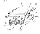
- FIG. 1 illustrates a structure of a conventional plasma display panel.
- a plasma display panel includes a front panel 100 and a rear panel 110.
- the front panel 100 has a plurality of sustain electrode pairs arranged with a scan electrode 102 and a sustain electrode 103 each paired and formed on a front glass 101, which is a display surface for displaying the image thereon.
- the rear panel 110 has a plurality of address electrodes 113 arranged to intersect with the plurality of sustain electrode pairs on a rear glass 111, which is spaced apart in parallel with and sealed to the front panel 100.
- the front panel 100 includes the paired scan electrode 102 and the paired sustain electrode 103 for performing a mutual discharge in one pixel and sustaining an emission of light.
- Each of the paired scan electrode 102 and the paired sustain electrode 103 has a transparent electrode (a) formed of indium-tin-oxide (ITO) and a bus electrode (b) formed of metal.
- the scan electrode 102 and the sustain electrode 103 are covered with at least one dielectric layer 104, which controls a discharge current and insulates the paired electrodes.
- a protective layer 105 is formed of oxide magnesium (MgO) on the dielectric layer 104 to facilitate a discharge condition.
- MgO oxide magnesium
- the rear panel 110 includes stripe-type (or well-type) barrier ribs 112 for forming a plurality of discharge spaces or discharge cells arranged in parallel.
- the rear panel 110 includes a plurality of address electrodes 113 performing an address discharge are arranged in parallel with the barrier ribs 112. Red (R), green (G) and blue (B) phosphors 114 emit visible light for displaying the image in the sustain discharge and are coated over an upper surface of the rear panel 110.
- a dielectric layer 115 for protecting the address electrode 113 is formed between the address electrode 113 and the phosphor 114.
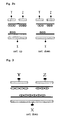
- FIG. 2a illustrates driving waveforms of a prior art plasma display panel.
- the plasma display panel is driven with a frame divided into a reset period for initializing the entire cells, an address period for selecting a cell to be discharged, a sustain period for sustaining the discharge of the selected cell and an erase period for erasing wall charges within discharged cells.
- a ramp-up waveform (Ramp-up) is applied to the entire scan electrodes at the same time.
- the ramp-up waveform generates a weak dark discharge within discharge cells of the entire screen.
- the setup discharge causes positive wall charges to be accumulated on the address electrodes and the sustain electrodes, negative wall charges to be accumulated on the scan electrodes.
- a ramp-down waveform (Ramp-down), which starts falling from a positive voltage lower than a peak voltage of the ramp-up waveform up to a predetermined voltage level lower than a ground (GND) level voltage, generates a weak erase discharge within cells, thereby sufficiently erasing wall charges excessively formed on the scan electrodes. Wall charges sufficient for a stable address discharge are uniformly remained within the cells due to the the setdown discharge.
- address pulses having a positive polarity is applied to the address electrodes in synchronization with the scan pulse.
- a voltage difference between the scan pulse and the address pulse and a wall voltage generated in the reset period are added, an address discharge is generated within discharge cells to which the address pulse is applied.
- Wall charges that can cause a discharge when a sustain voltage (Vs) is applied are generated within cells selected by an address discharge.
- the sustain electrodes are supplied with a positive voltage (Vz) in order that an erroneous discharge is not generated between the sustain electrode and the scan electrode by reducing the voltage difference between the sustain electrode and the scan electrode during the setdown period and the address period.
- a sustain pulse is alternately applied to the scan electrodes and the sustain electrodes.
- a sustain discharge i.e., a display discharge is generated between the scan electrodes and the sustain electrodes whenever the sustain pulse is applied as the wall voltage within the cell and the sustain pulse are added.
- an erase ramp waveform (Ramp-ers) having a narrow pulse width and a low voltage level is applied to the sustain electrodes, thereby wall charges remaining within the cells of the entire screen are erased.
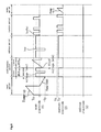
- FIG. 2b illustrates wall charges distributed in a discharge cell according to driving pulses of the prior art.
- the plasma display panel of the prior art described above is able to generate a stable address discharge, only when optimized wall charges are formed during the reset period. However, sometimes, one can not obtain optimized wall charges according to the characteristics of the panel, which results in an error discharge and or an error writing of discharge cell.
- FIG. 3 illustrates wall charges formed in some discharge cells among discharge cells according to driving pulses of the prior art.
- negative wall charges are formed in the scan electrode(Y)
- excessive positive wall charges are formed in an address electrode(X), in set down period.
- the positive wall charges excessively formed in the address electrode(X) undesirably performs an address discharge within the discharge cell to which data pulse is not applied. Therefore, a luminescent spot error discharge or a mistaken writing are happened to deteriorate the definition of a plasma display panel.
- the present invention seeks to provide an improved plasma display panel.
- United States Patent Application Publication No. US 2005/0225509 A1 discloses a driving method of a plasma display panel in which first and second electrodes are formed in parallel. Third electrodes respectively cross the first and second electrodes. Discharge cells are formed by adjacent first and second electrodes, and third electrodes.
- a main reset pulse has a waveform falling after rising to a second voltage from a first voltage.
- a sub reset pulse has a waveform falling from a third voltage to a fourth voltage.
- the main reset pulse and the sub reset pulse selectively are applied to a plurality of subfields.
- a misfiring erase pulse is applied after the main reset pulse is applied during a reset period of a subfield to which the main reset pulse is initially applied.
- the present invention seeks to provide an improved plasma display panel.
- Embodiments of the invention can provide a plasma display panel capable of preventing an error discharge and an error writing of a discharge cell.
- a first aspect of the invention provides a plasma display apparatus according to claim 1.
- FIG. 1 illustrates a structure of a conventional plasma display panel.
- FIG. 2a illustrates driving waveforms of a plasma display panel of a related art.
- FIG. 2b illustrates wall charges distributed in a discharge cell according to driving pulses of a related art.
- FIG. 3 illustrates wall charges formed in some discharge cells among discharge cells according to driving pulses of a related art.
- FIG. 4 illustrates a structure of a plasma display apparatus according to embodiments of the present invention.
- FIG. 5a illustrates an example of driving waveforms of a plasma display apparatus according to a first embodiment of the present invention.
- FIG. 5b illustrates wall charges distributed in a discharge cell due to a driving pulse according to a first embodiment of the present invention.
- FIG. 6 illustrates another example of driving waveforms of a plasma display apparatus according to a first embodiment of the present invention.
- FIG. 7 illustrates still another example of driving waveforms of a plasma display apparatus according to a first embodiment of the present invention.
- FIG. 8a illustrates an example of driving waveforms of a plasma display apparatus according to a second embodiment of the present invention.
- FIG. 8b illustrates wall charges distributed in a discharge cell due to a driving pulse according to a second embodiment of the present invention.
- FIG. 9 illustrates another example of driving waveforms of a plasma display apparatus according to a second embodiment of the present invention.
- FIG. 10 illustrates still another example of driving waveforms of a plasma display apparatus according to a second embodiment of the present invention.
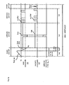
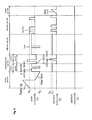
- FIG. 4 to FIG. 7 a plasma display apparatus according to a first embodiment will be described.
- plasma display apparatus comprises a plasma display panel 400, a data driver 410, a scan driver 420, a sustain driver 430, a driving pulse controller 440 and a driving voltage generator 450.
- the plasma display panel 420 comprises a plurality of scan electrodes Y1 to Yn, a plurality of sustain electrodes z and a plurality of address electrodes X1 to Xm that intersect the scan electrodes Y1 to Yn and the sustain electrodes z.
- the data driver 410 applies a data to address electrodes X1 to Xm formed in the plasma display panel 400.
- the data means an image signal data which is processed in an image signal processor(not shown) where image signals inputted from the outside are processed.
- the data driver 410 samples and latches the data in response to a data timing control signal CTRX from the driving pulse controller 440, and then supplies the address pulses having an address voltage Va to address electrodes X1 to Xm.
- the driving pulse controller 440 controls the data driver 410, the scan driver 420 and the sustain driver 430, when the plasma display panel 400 is driven.
- the driving pulse controller 440 generates timing control signals CTRX, CTRY, CTRZ for controlling an operation timing and synchronization of the data driver 410, the scan driver 420 and the sustain driver 430 during a reset period, an address period and a sustain period, transmits the timing control signals CTRX, CTRY, CTRZ to each driver 410, 420, 430.
- the data control signal CTRX includes a sampling clock for sampling data, a latch control signal and a switch control signal for controlling the on/off time of an energy recovery circuit in the data driver 410 and a driving switch device.
- the scan control signal CTRY includes a switch control signal for controlling the on/off time of an energy recovery circuit in the scan driver 420 and a driving switch device.
- the sustain control signal CTRZ includes a switch control signal for controlling the on/off time of an energy recovery circuit in the sustain driver 430 and a driving switch device.
- the scan driver 420 drives the scan electrodes Y1 to Yn formed in the plasma display panel 400.
- the scan driver 420 under the control of the driving pulse controller 440, supplies set-up pulse and set-down pulse representing a ramp-waveform formed by the combination of Vs, Vsetup and - Vy to the scan electrodes Y1 to Yn during reset period.
- the driving pulse controller 440 applies, between a reset pulse and a negative scan pulse, a negative waveform and a positive waveform to the scan electrodes by the scan driver 420.
- the negative waveform performs erasing wall charges excessively accumulated in the address electrodes X1 to Xm of the discharge cells which are not turned off.
- the positive waveform performs erasing wall charges excessively accumulated in the scan electrodes Y1 to Yn and the sustain electrodes z.
- the driving pulse controller 440 supplies a reference voltage to the sustain electrodes z when the positive waveform is applied the scan electrode, supplies a suatain bias voltage to the sustain electrodes z when the negative waveform is applied the scan electrode, by the sustain driver 430 for erasing some wall charges.
- FIG. 5a to FIG. 7 it will be described in detail.
- a scan pulse apllied from a scan reference voltage Vsc to a scan voltage -Vy is sequentially applied to each of the scan electrodes Y1 to Yn during the address period.
- the scan driver 420 applies at least one sustain pulse applied from a ground level to a sustain voltage Vs to the scan electrodes Y1 to Yn for sustain discharge during the sustain period.
- the sustain driver 430 drives the sustain electrodes z formed as a common electrode in the plasma display panel 400.
- the driving pulse controller 440 according to the first embodiment supplies the reference voltage GND to the sustain electrodes z when the positive waveform is applied the scan electrodes Y1 to Yn, supplies the suatain bias voltage to the sustain electrodes z when the negative waveform is applied the scan electrode.
- the driving pulse controller 440 applies the bias voltage to the sustain electrodes z during the address period, applies at least one sustain pulse, applied from the reference voltage level GND to a sustain voltage Vs, to the sustain electrodes z for sustain discharge during the sustain period.
- the driving voltage generator 450 generates and supplies a driving voltage for the driving pulse controller 440 and each driver 410, 420, 430.
- the driving voltage generator 450 generates a set-up voltage Vsetup, a scan reference voltage Vsc, a scan voltage -Vy, a sustain voltage Vs, an address voltage Va and a bias voltage Vzb.
- the driving voltages described above can be controlled depending on the composition of a discharge gas or the structure of a discharge cell.
- Driving pulses applied to a plasma display apparatus according to the first embodiment and wall charges distributed in the plasma display panel are shown in FIG. 5a to FIG. 5b .
- the plasma display apparatus is driven with a reset period for initializing all discharge cells, a stabilization period for stabilizing excessive wall charges distribution within the discharge cell, an address period for selecting a discharge cell, a sustain period for sustaining discharge of the selected cell and an erase priod for erasing wall charges within the discharged cell.
- Ramp-up waveform is simultaneously applied to all scan electrodes in set-up period. This Ramp-up waveform causes dark discharges within discharge cells of the entire screen. Due to this set-up discharge, positive wall charges are accumulated in the address electrode and the sustain electrode, negative wall charges are accumulated in the scan electrode.
- Ramp-down waveform falling from the reference voltage level GND to a predetermined voltage level -Vy generates an erase discharge between the scan electrode and the sustain electrode.
- wall charges formed between the scan electrode and the sustain electrode are enoughly erased. Due to this set-down discharge, wall charges enough to generate a stable address discharge are uniformly remained within the cells.
- the first embodiment selectively erases wall charges formed between the scan electrode and the sustain electrode for preventing an error discharge due to a residual image.
- the positive waveform and the negative waveform are applied to the scan electrode between the reset pulse and the negative scan pulse.
- the negative waveform is a rectangular waveform.
- the negative waveform is applied from a first voltage level.
- the first voltage level lies in the range from -90V to -70V and the peak voltage of the negative waveform lies in the range from -210V to -190V.
- the width of the negative waveform is approximately the same with the width of the scan pulse or wider than the width of the scan pulse.
- the width of the negative waveform lies in the range from 1 ⁇ s to 10 ⁇ s.
- the width and magnitude of the waveform are set so as to erase some negative wall charges of the scan electrode and a part of excessive positive wall charges of the address electrode in proper.
- the sustain bias voltage Vz is applied to the sustain electrode when the negative waveform is applied to the scan electrode.
- the sustain bias voltage Vz lies in the range from 80V to 100V. Due to the application of the negative waveform, a weak erase discharge is happened between the scan electrode and the address electrode.
- a positive waveform is then applied to the scan electrode after the negative waveform has been applied to the scan electrode.
- the positive waveform is a rising waveform rises from the first voltage level with a predetermined slope.
- the positive rising waveform rises to a voltage level that is approximately the same with a sustain pulse voltage level Vs applied during the sustain period after the address period.
- the peak voltage level of the positive waveform lies in the range from 150V to 250V. Accordingly, wall charges, which are enough for a stable address discharge in the scan electrode Y and the sustain electrode Z, uniformly remain.
- a reference voltage is applied to the sustain electrode when the positive waveform is applied to the scan electrode.
- the negative scan pulse is sequentially applied to the scan electrodes, while the positive address pulse is applied to the address electrodes in synchronization with the scan pulse.
- the address discharge occurs in the discharge cell to which the address pulse is applied, by adding the voltage difference between the scan pulse and the address pulse to the wall voltage formed during the reset period. Wall charges sufficient for discharge by the sustain voltage are formed within the cells selected by address discharge.
- a positive sustain bias voltage Vz is applied to the sustain electrode so that an error discharge between the scan electrode and the sustain electrode will not take place by decreasing the voltage difference between the scan electrode and the sustain electrode during the set-down period and the address period.
- the sustain pulse Sus having the magnitude of sustain voltage Vs is alternately applied to the scan electrode and the sustain electrode.
- a sustain discharge between the scan electrode and the sustain electrode that is, a display discharge takes place whenever the sustain pulse is applied by adding wall charges within the cell to the sustain pulse.
- negative wall charges are formed in a scan electrode Y during the set-down period of the reset period, excessive positive wall charges are formed in an address electrode X (a).
- a negative waveform is applied to the scan electrode Y, which causes some of negative wall charges in the scan electrode Y and some of excessive positive wall charges in the address electrodes X to be erased (b).
- a positive waveform is applied to the scan electrode Y, a reference voltage is applied to the sutain electrode Z.
- Wall charges sufficient for a stable address discharge between the scan electrode Y and the sutain electrode Z uniformly remain (c). Accordingly, an erroneous writing or a luminescent spot error discharge can be prevented.
- FIG. 6 illustrates another example of driving waveforms of the plasma display apparatus according to the first embodiment.
- the driving pulse applied in a reset period, an address period, a sustain period and an erase period is the same as the driving pulse shown in FIG. 5a .
- a negative waveform applied to a scan electrode Y is applied from a second voltage level.
- the second voltage level different from the first voltage level of FIG. 5a , is positive and applied from the voltage level which lies in the range from 50V to 80V. Accordingly, the lowest voltage level lies in the range from -70V to -40V.
- the positive rising waveform described above rises from a third voltage level. In this exemplary embodiment, the third voltage level lies in the range from -10V to 10V.
- FIG. 7 illustrates still another example of driving waveforms of the plasma display apparatus according to the first embodiment.
- the driving pulse applied in a reset period, a sustain period and an erase pulse is the same as the driving pulse shown in FIG. 5a .
- the bias voltage applied to a scan electrode Y during address period is lower than a reference voltage.
- the negative waveform applied to the scan electrode Y is applied from a second voltage level which is different from the first voltage level of FIG. 5a .
- the second voltage level is a ground voltage.
- the positive rising waveform described above rises from a third voltage level.
- the third voltage level lies in the range from from -10V to 10V.
- a plasma display apparatus will now be described with reference to FIG. 4 and FIGs. 8a to FIG. 10 .
- the plasma display apparatus according to the second embodiment is the same as the plasma display apparatus according to the first embodiment, except for the sustain driver and the scan driver. Hence, the explanation of elements other than the sustain driver and the scan driver will be abbreviated.
- a controller 440 applies a negative waveform and a positive waveform by a scan driver 420 between a reset pulse and a negative scan pulse.
- the positive waveform and the negative waveform are respective rectangular pulses.
- the negative waveform described above is a pulse for erasing wall charges excessively accumulated in address electrodes X1 to Xn of the cells that are not turned on.
- the positive waveform described above is a pulse for erasing wall charges excessively accumulated in scan electrodes Y1 to Yn and sustain electrodes Z.
- the controller 440 applies a positive waveform to the sustain electrode Z by a sustain driver 430 alternately with the positive waveform described above. A more detailed description will be given through FIG. 8a to FIG. 10 .
- the controller 440 applies a positive waveform to the sustain electrode Z by a sustain driver 430 alternately with the positive waveform described above applied to the scan electrodes Y1 to Yn under the control of a driving pulse controller 450.
- the positive waveform applied to the sustain electrode Z is a narrow pulse.
- the narrow pulse is a pulse having a width less than the width of the sustain pulse, being applied for erasing wall charges.
- the width of the narrow pulse it is preferable for the width of the narrow pulse to be less than half the width of the sustain pulse.
- FIG. 8a and FIG. 8b the driving pulse implemented by a plasma display panel according to the second embodiment and the distribution of wall charges in the plasma display panel are illustated.
- the plasma display apparatus is driven by time-division, with a reset period for initializing the entire cells, a stabilization period for stabilizing excessive wall charges within a discharge cell, an address period for selecting a cell to be discharged, a sustain period for sustaining the discharge of the selected cell and an erase period for erasing wall charges within the discharged cells.
- a rising ramp waveform Ramp-up is simultaneously applied to all the scan electrodes. Due to the rising ramp waveform, a dark discharge takes place within the discharge cells of the entire screen. Due to the set up discharge, positive wall charges become accumulated in the address electrode and the sustain electrode, while negative wall charges become accumulated in the scan electrode.
- a falling ramp waveform falls from a reference volage level GND to a predetermined voltage level -Vy causes an erase discharge between the scan electrode and the address electrode in the cells. Accordingly, wall charges formed between the scan electrode and the address electrode are sufficiently erased. Due to the set-down discharge, wall charges enough for a stable address discharge uniformly remain in the cells.
- the second embodiment selectively erases wall charges formed between the scan electrode and the sustain electrode in order to prevent an erroneous discharge due to a residual image.
- a negative waveform and a positive waveform between the reset pulse and the negative scan pulse, are applied to the scan electrode.
- the negative waveform and the positive waveform described above are respective rectangular pulses, being applied from a first voltage level.
- the first voltage level lies in the range from -90V to -70V and the lowest voltage level of the negative waveform, that is, the peak value of the negative waveform, lies in the range from -210V to -190V.
- the width of the negative waveform is approximately the same as, or wider than, the width of the scan pulse applied to the scan electrode during the address period.
- the width of the negative waveform lies in the range from 1 ⁇ s to 10 ⁇ s. The width and the magnitude of the negative waveform are properly set, such that it is possible to erase some of the negative wall charges in the scan electrode described above and some of the excessive positive wall charges in the address electrode.
- a sustain bias voltage is applied to the sustain electrode.
- a narrow pulse having a width less than half of the sustain pulse width is applied to the sustain electrode after the positive waveform has been applied to the scan electrode.
- the sustain bias voltage level Vz ranges from 80V to 100V which is lower than a sustain voltage. Due to the application of the negative waveform, a dark discharge occurs between the scan electrode and the address electrode.
- a positive waveform is applied to the scan electrode after the negative waveform is applied to the scan electrode.
- the positive waveform applied to the scan electrode is a rectangular pulse, rising from the first voltage level to a voltage level that is approximately the same with the voltage level of the sustain pulse Vs applied during the sustain period after the address period, and the peak voltage level of the positive waveform lies in the range from 150V to 250V.
- a positive waveform is alternately applied to the sustain electrode with the positive waveform applied to the scan electrode.
- the positive waveform applied to the sustain electrode is a narrow pulse.
- the peak voltage level of the positive waveform applied to the sustain electrode is a voltage level that is approximately the same as the voltage level of the sustain pulse Vs applied during the sustain period after the address period.
- the peak voltage level of the positive waveform applied to the sustain electrode lies in the range from 150V to 250V.
- the negative waveform and the positive waveform applied to the scan electrode Y are applied from the reference voltage.
- an address period negative scan pulses are sequentially applied to scan electrodes, while a positive address pulse is applied to an address electrode in synchronization with the scan pulse.
- a positive address pulse is applied to an address electrode in synchronization with the scan pulse.
- an address discharge takes place within a discharge cell to which the address pulse is applied.
- Wall charges sufficient for a discharge with the application of a sustain voltage Vs are formed within cells selected by the address discharge.
- a positive bias voltage is applied to the sustain electrode by decreasing the voltage difference between the sustain electrode and the scan electrode for preventing an error discharge.
- sustain pulses are alternately applied to the scan electrode and the sustain electrode.
- a sustain discharge or a display discharge takes place between the scan electrode and the sustain electrode by adding the wall voltage within the cell to the sustain pulse whenever each sustain pulse is applied to the scan electrode and the sustain electrode.
- an erase ramp waveform Ramp-ers having small width and low voltage level is applied to the sustain electrode to erase wall charges remaining in the entire cells.
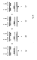
- FIG. 8b illustrates wall charges distributed in a discharge cell due to a driving pulse according to a second embodiment.
- negative wall charges are formed in a scan electrode Y during the set-down period of a reset period, excessive positive wall charges are formed in an address electrode X (a).
- a negative waveform is applied to the scan electrode Y, which causes that some of the negative wall charges in the scan electrode Y and some of the excessive positive wall charges in the address electrodes X to be erased (b).
- a positive waveform is applied to the scan electrode Y, while a positive narrow pulse is applied to the sustain electrode Z alternately with the positive waveform applied to the scan electrode Y. Accordingly, excessive wall charges in the scan electrode Y and the sustain electrode Z are erased(c). Then, wall charges sufficient for a stable address discharge between the scan electrode Y and the sutain electrode Z uniformly remain (d). Thus, erroneous writing or a luminescent spot error discharge can be prevented.
- FIG. 9 illustrates another example of driving waveforms of a plasma display apparatus according to a second embodiment.
- the driving pulse applied in a reset period, an address period, a sustain period and an erase period is the same with the driving pulse shown in FIG. 8a .
- a negative waveform applied to a scan electrode Y is applied from a second voltage level.
- the second voltage level different from the embodiment of FIG. 8a , is positive and applied from the voltage level which lies in the range from 50V to 80V. Accordingly, the lowest voltage level lies in the range from -70V to -40V.
- the positive rising waveform applied to the scan electrode rises from a third voltage level.
- the third voltage level lies in the range from -10V to 10V. Accordingly, wall charges can be properly erased according to the amount of wall charges accumulated in an address electrode X.
- FIG. 10 illustrates still another example of driving waveforms of a plasma display apparatus according to a second embodiment.
- the driving pulse applied in a reset period, a sustain period and an erase period is the same as the driving pulse shown in FIG. 8a .
- a bias voltage applied to the scan electrode Y during an address period may be lower than a reference voltage.
- a negative waveform applied to a scan electrode Y is applied from a second voltage level.
- the second voltage level lies in the range from -10V to 10V.
- the lowest voltage level of the negative waveform lies in the range from -70V to -40V.
- the positive rising waveform applied to the scan electrode rises from a third voltage level.
- the third voltage level lies n the range from -10V to 10V. Accordingly, wall charges can be properly erased according to the amount of wall charges accumulated in an address electrode X.
Description
- This invention relates to a plasma display panel. It more particularly relates to a plasma display apparatus capable of preventing an error discharge or an error writing of a discharge cell.
- In a conventioal plasma display panel, one unit cell is provided at a space between barrier ribs formed between a front panel and a rear panel. A main discharge gas such as neon (Ne), helium (He) or a mixture (He+Ne) of neon and helium and an inert gas containing a small amount of xenon (Xe) fill each cell. When a discharge occurs using a high frequency voltage, the inert gas generates vacuum ultraviolet radiation and phosphors provided between the barrier ribs are stimulated to emit light, thereby realizing an image. The plasma display panel is considered as one of the next generation display devices due to its thin profile and light weigh construction.
-
FIG. 1 illustrates a structure of a conventional plasma display panel. - As shown in
FIG. 1 , a plasma display panel includes afront panel 100 and arear panel 110. Thefront panel 100 has a plurality of sustain electrode pairs arranged with ascan electrode 102 and asustain electrode 103 each paired and formed on afront glass 101, which is a display surface for displaying the image thereon. Therear panel 110 has a plurality ofaddress electrodes 113 arranged to intersect with the plurality of sustain electrode pairs on arear glass 111, which is spaced apart in parallel with and sealed to thefront panel 100. - The
front panel 100 includes the pairedscan electrode 102 and the pairedsustain electrode 103 for performing a mutual discharge in one pixel and sustaining an emission of light. Each of the pairedscan electrode 102 and the pairedsustain electrode 103 has a transparent electrode (a) formed of indium-tin-oxide (ITO) and a bus electrode (b) formed of metal. Thescan electrode 102 and thesustain electrode 103 are covered with at least onedielectric layer 104, which controls a discharge current and insulates the paired electrodes. A protective layer 105 is formed of oxide magnesium (MgO) on thedielectric layer 104 to facilitate a discharge condition. - The
rear panel 110 includes stripe-type (or well-type)barrier ribs 112 for forming a plurality of discharge spaces or discharge cells arranged in parallel. Therear panel 110 includes a plurality ofaddress electrodes 113 performing an address discharge are arranged in parallel with thebarrier ribs 112. Red (R), green (G) and blue (B)phosphors 114 emit visible light for displaying the image in the sustain discharge and are coated over an upper surface of therear panel 110. Adielectric layer 115 for protecting theaddress electrode 113 is formed between theaddress electrode 113 and thephosphor 114. -
FIG. 2a illustrates driving waveforms of a prior art plasma display panel. - As shown in
FIG. 2a , the plasma display panel is driven with a frame divided into a reset period for initializing the entire cells, an address period for selecting a cell to be discharged, a sustain period for sustaining the discharge of the selected cell and an erase period for erasing wall charges within discharged cells. - In the setup period of the reset period, a ramp-up waveform (Ramp-up) is applied to the entire scan electrodes at the same time. The ramp-up waveform generates a weak dark discharge within discharge cells of the entire screen. The setup discharge causes positive wall charges to be accumulated on the address electrodes and the sustain electrodes, negative wall charges to be accumulated on the scan electrodes.
- In the setdown period of the reset period, after the ramp-up waveform is applied, a ramp-down waveform (Ramp-down), which starts falling from a positive voltage lower than a peak voltage of the ramp-up waveform up to a predetermined voltage level lower than a ground (GND) level voltage, generates a weak erase discharge within cells, thereby sufficiently erasing wall charges excessively formed on the scan electrodes. Wall charges sufficient for a stable address discharge are uniformly remained within the cells due to the the setdown discharge.
- In the address period, while negative scan pulses are sequentially applied to the scan electrodes, address pulses having a positive polarity is applied to the address electrodes in synchronization with the scan pulse. As a voltage difference between the scan pulse and the address pulse and a wall voltage generated in the reset period are added, an address discharge is generated within discharge cells to which the address pulse is applied. Wall charges that can cause a discharge when a sustain voltage (Vs) is applied are generated within cells selected by an address discharge. The sustain electrodes are supplied with a positive voltage (Vz) in order that an erroneous discharge is not generated between the sustain electrode and the scan electrode by reducing the voltage difference between the sustain electrode and the scan electrode during the setdown period and the address period.
- In the sustain period, a sustain pulse is alternately applied to the scan electrodes and the sustain electrodes. In a cell selected by an address discharge, a sustain discharge, i.e., a display discharge is generated between the scan electrodes and the sustain electrodes whenever the sustain pulse is applied as the wall voltage within the cell and the sustain pulse are added.
- After the sustain discharge is completed, in the erase period, an erase ramp waveform (Ramp-ers) having a narrow pulse width and a low voltage level is applied to the sustain electrodes, thereby wall charges remaining within the cells of the entire screen are erased.
- The distribution of wall charges in the discharge cell due to a driving pulse is shown in
FIG. 2b , which illustrates wall charges distributed in a discharge cell according to driving pulses of the prior art. - Referring to
FIG. 2b , during the setup period, negative wall charges are formed in the scan electrode(Y), positive wall charges are formed in the sustain electrode(Z). During the setdown period, Ramp-Down waveform, falling from a positive voltage lower than the peak voltage of Ramp-Up waveform, is applied to the scan electrode. Accordingly, excessive wall charges which are unnecessary and unbalanced are erased, therefore, wall charges within a cell are decreased in a moderate amount. - Then, during the address period, a negative voltage is applied to the scan electrode(Y), a positive voltage is applied to the sustain electrode(Z). In this time, an address discharge is happened by adding the voltage, negative, of wall charges formed in a setdown period to the negative voltage applied to the scan electrode(Y).
- The plasma display panel of the prior art described above is able to generate a stable address discharge, only when optimized wall charges are formed during the reset period. However, sometimes, one can not obtain optimized wall charges according to the characteristics of the panel, which results in an error discharge and or an error writing of discharge cell.
-
FIG. 3 illustrates wall charges formed in some discharge cells among discharge cells according to driving pulses of the prior art. As shown inFIG. 3 , in some discharge cells, negative wall charges are formed in the scan electrode(Y), excessive positive wall charges are formed in an address electrode(X), in set down period. As described above, the positive wall charges excessively formed in the address electrode(X) undesirably performs an address discharge within the discharge cell to which data pulse is not applied. Therefore, a luminescent spot error discharge or a mistaken writing are happened to deteriorate the definition of a plasma display panel. - The present invention seeks to provide an improved plasma display panel.
- United States Patent Application Publication No.
US 2005/0225509 A1 discloses a driving method of a plasma display panel in which first and second electrodes are formed in parallel. Third electrodes respectively cross the first and second electrodes. Discharge cells are formed by adjacent first and second electrodes, and third electrodes. A main reset pulse has a waveform falling after rising to a second voltage from a first voltage. A sub reset pulse has a waveform falling from a third voltage to a fourth voltage. The main reset pulse and the sub reset pulse selectively are applied to a plurality of subfields. A misfiring erase pulse is applied after the main reset pulse is applied during a reset period of a subfield to which the main reset pulse is initially applied. - The present invention seeks to provide an improved plasma display panel.
- Embodiments of the invention can provide a plasma display panel capable of preventing an error discharge and an error writing of a discharge cell.
- A first aspect of the invention provides a plasma display apparatus according to
claim 1. - Other aspects of the invention are defined in the sub-claims.
- Embodiments of the invention will now be described by way of non-limiting example only, with reference to the drawings, in which:
-
FIG. 1 illustrates a structure of a conventional plasma display panel. -
FIG. 2a illustrates driving waveforms of a plasma display panel of a related art. -
FIG. 2b illustrates wall charges distributed in a discharge cell according to driving pulses of a related art. -
FIG. 3 illustrates wall charges formed in some discharge cells among discharge cells according to driving pulses of a related art. -
FIG. 4 illustrates a structure of a plasma display apparatus according to embodiments of the present invention. -
FIG. 5a illustrates an example of driving waveforms of a plasma display apparatus according to a first embodiment of the present invention. -
FIG. 5b illustrates wall charges distributed in a discharge cell due to a driving pulse according to a first embodiment of the present invention. -
FIG. 6 illustrates another example of driving waveforms of a plasma display apparatus according to a first embodiment of the present invention. -
FIG. 7 illustrates still another example of driving waveforms of a plasma display apparatus according to a first embodiment of the present invention. -
FIG. 8a illustrates an example of driving waveforms of a plasma display apparatus according to a second embodiment of the present invention. -
FIG. 8b illustrates wall charges distributed in a discharge cell due to a driving pulse according to a second embodiment of the present invention. -
FIG. 9 illustrates another example of driving waveforms of a plasma display apparatus according to a second embodiment of the present invention. -
FIG. 10 illustrates still another example of driving waveforms of a plasma display apparatus according to a second embodiment of the present invention. - Referring to
FIG. 4 to FIG. 7 , a plasma display apparatus according to a first embodiment will be described. - As shown in
FIG. 4 , plasma display apparatus comprises aplasma display panel 400, adata driver 410, ascan driver 420, a sustaindriver 430, a drivingpulse controller 440 and a drivingvoltage generator 450. - The
plasma display panel 420 comprises a plurality of scan electrodes Y1 to Yn, a plurality of sustain electrodes z and a plurality of address electrodes X1 to Xm that intersect the scan electrodes Y1 to Yn and the sustain electrodes z. - The
data driver 410 applies a data to address electrodes X1 to Xm formed in theplasma display panel 400. In this case, the data means an image signal data which is processed in an image signal processor(not shown) where image signals inputted from the outside are processed. - The
data driver 410 samples and latches the data in response to a data timing control signal CTRX from the drivingpulse controller 440, and then supplies the address pulses having an address voltage Va to address electrodes X1 to Xm. - The driving
pulse controller 440 controls thedata driver 410, thescan driver 420 and the sustaindriver 430, when theplasma display panel 400 is driven. - In other words, the driving
pulse controller 440 generates timing control signals CTRX, CTRY, CTRZ for controlling an operation timing and synchronization of thedata driver 410, thescan driver 420 and the sustaindriver 430 during a reset period, an address period and a sustain period, transmits the timing control signals CTRX, CTRY, CTRZ to eachdriver - The data control signal CTRX includes a sampling clock for sampling data, a latch control signal and a switch control signal for controlling the on/off time of an energy recovery circuit in the
data driver 410 and a driving switch device. The scan control signal CTRY includes a switch control signal for controlling the on/off time of an energy recovery circuit in thescan driver 420 and a driving switch device. The sustain control signal CTRZ includes a switch control signal for controlling the on/off time of an energy recovery circuit in the sustaindriver 430 and a driving switch device. - The
scan driver 420 drives the scan electrodes Y1 to Yn formed in theplasma display panel 400. Thescan driver 420, under the control of the drivingpulse controller 440, supplies set-up pulse and set-down pulse representing a ramp-waveform formed by the combination of Vs, Vsetup and - Vy to the scan electrodes Y1 to Yn during reset period. - The driving
pulse controller 440 according to the first embodiment applies, between a reset pulse and a negative scan pulse, a negative waveform and a positive waveform to the scan electrodes by thescan driver 420. The negative waveform performs erasing wall charges excessively accumulated in the address electrodes X1 to Xm of the discharge cells which are not turned off. The positive waveform performs erasing wall charges excessively accumulated in the scan electrodes Y1 to Yn and the sustain electrodes z. The drivingpulse controller 440 supplies a reference voltage to the sustain electrodes z when the positive waveform is applied the scan electrode, supplies a suatain bias voltage to the sustain electrodes z when the negative waveform is applied the scan electrode, by the sustaindriver 430 for erasing some wall charges. InFIG. 5a to FIG. 7 , it will be described in detail. - Then, a scan pulse apllied from a scan reference voltage Vsc to a scan voltage -Vy is sequentially applied to each of the scan electrodes Y1 to Yn during the address period.
- The
scan driver 420 applies at least one sustain pulse applied from a ground level to a sustain voltage Vs to the scan electrodes Y1 to Yn for sustain discharge during the sustain period. - The sustain
driver 430 drives the sustain electrodes z formed as a common electrode in theplasma display panel 400. [72] The drivingpulse controller 440 according to the first embodiment supplies the reference voltage GND to the sustain electrodes z when the positive waveform is applied the scan electrodes Y1 to Yn, supplies the suatain bias voltage to the sustain electrodes z when the negative waveform is applied the scan electrode. The drivingpulse controller 440 applies the bias voltage to the sustain electrodes z during the address period, applies at least one sustain pulse, applied from the reference voltage level GND to a sustain voltage Vs, to the sustain electrodes z for sustain discharge during the sustain period. - The driving
voltage generator 450 generates and supplies a driving voltage for the drivingpulse controller 440 and eachdriver voltage generator 450 generates a set-up voltage Vsetup, a scan reference voltage Vsc, a scan voltage -Vy, a sustain voltage Vs, an address voltage Va and a bias voltage Vzb. The driving voltages described above can be controlled depending on the composition of a discharge gas or the structure of a discharge cell. Driving pulses applied to a plasma display apparatus according to the first embodiment and wall charges distributed in the plasma display panel are shown inFIG. 5a to FIG. 5b . - As shown in
FIG. 5a , the plasma display apparatus according to the first embodiment is driven with a reset period for initializing all discharge cells, a stabilization period for stabilizing excessive wall charges distribution within the discharge cell, an address period for selecting a discharge cell, a sustain period for sustaining discharge of the selected cell and an erase priod for erasing wall charges within the discharged cell. - In the reset period, Ramp-up waveform is simultaneously applied to all scan electrodes in set-up period. This Ramp-up waveform causes dark discharges within discharge cells of the entire screen. Due to this set-up discharge, positive wall charges are accumulated in the address electrode and the sustain electrode, negative wall charges are accumulated in the scan electrode.
- In the set-down period, Ramp-down waveform falling from the reference voltage level GND to a predetermined voltage level -Vy generates an erase discharge between the scan electrode and the sustain electrode. Thus, wall charges formed between the scan electrode and the sustain electrode are enoughly erased. Due to this set-down discharge, wall charges enough to generate a stable address discharge are uniformly remained within the cells.
- In the stabilization period, the first embodiment selectively erases wall charges formed between the scan electrode and the sustain electrode for preventing an error discharge due to a residual image. For the erasing, the positive waveform and the negative waveform are applied to the scan electrode between the reset pulse and the negative scan pulse. In this embodiment, the negative waveform is a rectangular waveform. However, this is not essential to the invention in its broadest aspect. The negative waveform is applied from a first voltage level. In this embodiment, the first voltage level lies in the range from -90V to -70V and the peak voltage of the negative waveform lies in the range from -210V to -190V. Preferably, but not essentially, the width of the negative waveform is approximately the same with the width of the scan pulse or wider than the width of the scan pulse. In this embodiment, the width of the negative waveform lies in the range from 1µs to 10µs. The width and magnitude of the waveform are set so as to erase some negative wall charges of the scan electrode and a part of excessive positive wall charges of the address electrode in proper.
- The sustain bias voltage Vz is applied to the sustain electrode when the negative waveform is applied to the scan electrode. In this embodiment, the sustain bias voltage Vz lies in the range from 80V to 100V. Due to the application of the negative waveform, a weak erase discharge is happened between the scan electrode and the address electrode.
- A positive waveform is then applied to the scan electrode after the negative waveform has been applied to the scan electrode. In this case, the positive waveform is a rising waveform rises from the first voltage level with a predetermined slope. The positive rising waveform rises to a voltage level that is approximately the same with a sustain pulse voltage level Vs applied during the sustain period after the address period. In this embodiment, the peak voltage level of the positive waveform lies in the range from 150V to 250V. Accordingly, wall charges, which are enough for a stable address discharge in the scan electrode Y and the sustain electrode Z, uniformly remain.
- A reference voltage is applied to the sustain electrode when the positive waveform is applied to the scan electrode.
- By performing the erase discharge, excessive wall charges accumulated in the cells, which are turned off in the region representing a single color pattern during operation, are selectively erased to efficiently improve a luminescent spot problem. A further detailed explanation will be given with reference to
FIG. 5b . - During the address period, the negative scan pulse is sequentially applied to the scan electrodes, while the positive address pulse is applied to the address electrodes in synchronization with the scan pulse. The address discharge occurs in the discharge cell to which the address pulse is applied, by adding the voltage difference between the scan pulse and the address pulse to the wall voltage formed during the reset period. Wall charges sufficient for discharge by the sustain voltage are formed within the cells selected by address discharge. A positive sustain bias voltage Vz is applied to the sustain electrode so that an error discharge between the scan electrode and the sustain electrode will not take place by decreasing the voltage difference between the scan electrode and the sustain electrode during the set-down period and the address period.
- During the sustain period, the sustain pulse Sus having the magnitude of sustain voltage Vs is alternately applied to the scan electrode and the sustain electrode. In the cell selected by the address discharge, a sustain discharge between the scan electrode and the sustain electrode, that is, a display discharge takes place whenever the sustain pulse is applied by adding wall charges within the cell to the sustain pulse.
- After the completion of sustain discharge, during the erase period, an erase ramp waveform Ramp-ers having a small pulse width and a low voltage level is applied to the sustain electrode, then, wall charges remaining in the cells of the entire screen are erased. The explanation about wall charges distributed within the cell due to a driving pulse according to a first embodiment of the present invention will be described with reference to
FIG. 5b . - Referring
FIG.5 , negative wall charges are formed in a scan electrode Y during the set-down period of the reset period, excessive positive wall charges are formed in an address electrode X (a). During a stabilization period, before an address period, a negative waveform is applied to the scan electrode Y, which causes some of negative wall charges in the scan electrode Y and some of excessive positive wall charges in the address electrodes X to be erased (b). During a second stabilization period before the address period, a positive waveform is applied to the scan electrode Y, a reference voltage is applied to the sutain electrode Z. Wall charges sufficient for a stable address discharge between the scan electrode Y and the sutain electrode Z uniformly remain (c). Accordingly, an erroneous writing or a luminescent spot error discharge can be prevented. -
FIG. 6 illustrates another example of driving waveforms of the plasma display apparatus according to the first embodiment. - As shown in
FIG. 6 , the driving pulse applied in a reset period, an address period, a sustain period and an erase period is the same as the driving pulse shown inFIG. 5a . In a first stabilization period, a negative waveform applied to a scan electrode Y is applied from a second voltage level. In other words, the second voltage level, different from the first voltage level ofFIG. 5a , is positive and applied from the voltage level which lies in the range from 50V to 80V. Accordingly, the lowest voltage level lies in the range from -70V to -40V. The positive rising waveform described above rises from a third voltage level. In this exemplary embodiment, the third voltage level lies in the range from -10V to 10V. Thus, wall charges are properly erased according to the amount of wall charges accumulated in an address electrode X. -
FIG. 7 illustrates still another example of driving waveforms of the plasma display apparatus according to the first embodiment. - As shown in
FIG. 7 , the driving pulse applied in a reset period, a sustain period and an erase pulse is the same as the driving pulse shown inFIG. 5a . In this embodiment, the bias voltage applied to a scan electrode Y during address period is lower than a reference voltage. In a first stabilization period, the negative waveform applied to the scan electrode Y is applied from a second voltage level which is different from the first voltage level ofFIG. 5a . Preferably, but not essentially, the second voltage level is a ground voltage. The positive rising waveform described above rises from a third voltage level. In this embodiment, it is preferable that the third voltage level lies in the range from from -10V to 10V. Thus, wall charges are properly erased according to the amount of wall charges accumulated in an address electrode X. - A plasma display apparatus according to a second embodiment will now be described with reference to
FIG. 4 andFIGs. 8a toFIG. 10 . The plasma display apparatus according to the second embodiment is the same as the plasma display apparatus according to the first embodiment, except for the sustain driver and the scan driver. Hence, the explanation of elements other than the sustain driver and the scan driver will be abbreviated. - A
controller 440 according to the second embodiment applies a negative waveform and a positive waveform by ascan driver 420 between a reset pulse and a negative scan pulse. In this embodiment, the positive waveform and the negative waveform are respective rectangular pulses. The negative waveform described above is a pulse for erasing wall charges excessively accumulated in address electrodes X1 to Xn of the cells that are not turned on. The positive waveform described above is a pulse for erasing wall charges excessively accumulated in scan electrodes Y1 to Yn and sustain electrodes Z. To erase some wall charges, thecontroller 440 applies a positive waveform to the sustain electrode Z by a sustaindriver 430 alternately with the positive waveform described above. A more detailed description will be given throughFIG. 8a to FIG. 10 . - The
controller 440 according to the second embodiment applies a positive waveform to the sustain electrode Z by a sustaindriver 430 alternately with the positive waveform described above applied to the scan electrodes Y1 to Yn under the control of a drivingpulse controller 450. In this embodiment, it is preferable that the positive waveform applied to the sustain electrode Z is a narrow pulse. - The narrow pulse is a pulse having a width less than the width of the sustain pulse, being applied for erasing wall charges. To erase wall charges according to the present embodiment, it is preferable for the width of the narrow pulse to be less than half the width of the sustain pulse.
- When the width of the narrow pulse is overly broad, it is difficult to erase wall charges. On the contrary, wall charges become accumulated in the cell, not erased.
- In
FIG. 8a andFIG. 8b , the driving pulse implemented by a plasma display panel according to the second embodiment and the distribution of wall charges in the plasma display panel are illustated. - Referring
FIG.8a , the plasma display apparatus according to the second embodiment is driven by time-division, with a reset period for initializing the entire cells, a stabilization period for stabilizing excessive wall charges within a discharge cell, an address period for selecting a cell to be discharged, a sustain period for sustaining the discharge of the selected cell and an erase period for erasing wall charges within the discharged cells. - In a reset period, during a set-up period, a rising ramp waveform Ramp-up is simultaneously applied to all the scan electrodes. Due to the rising ramp waveform, a dark discharge takes place within the discharge cells of the entire screen. Due to the set up discharge, positive wall charges become accumulated in the address electrode and the sustain electrode, while negative wall charges become accumulated in the scan electrode.
- During a set-down period, a falling ramp waveform falls from a reference volage level GND to a predetermined voltage level -Vy causes an erase discharge between the scan electrode and the address electrode in the cells. Accordingly, wall charges formed between the scan electrode and the address electrode are sufficiently erased. Due to the set-down discharge, wall charges enough for a stable address discharge uniformly remain in the cells.
- In the stabilization period, the second embodiment selectively erases wall charges formed between the scan electrode and the sustain electrode in order to prevent an erroneous discharge due to a residual image. To erase the wall charges, a negative waveform and a positive waveform, between the reset pulse and the negative scan pulse, are applied to the scan electrode. In this embodiment, the negative waveform and the positive waveform described above are respective rectangular pulses, being applied from a first voltage level. In this embodiment, the first voltage level lies in the range from -90V to -70V and the lowest voltage level of the negative waveform, that is, the peak value of the negative waveform, lies in the range from -210V to -190V.
- Preferably, but not essentially, the width of the negative waveform is approximately the same as, or wider than, the width of the scan pulse applied to the scan electrode during the address period. Preferably, but not essentially, the width of the negative waveform lies in the range from 1µs to 10µs. The width and the magnitude of the negative waveform are properly set, such that it is possible to erase some of the negative wall charges in the scan electrode described above and some of the excessive positive wall charges in the address electrode.
- When the negative waveform is applied to the scan electrode, a sustain bias voltage is applied to the sustain electrode. A narrow pulse having a width less than half of the sustain pulse width is applied to the sustain electrode after the positive waveform has been applied to the scan electrode. In this embodiment, the sustain bias voltage level Vz ranges from 80V to 100V which is lower than a sustain voltage. Due to the application of the negative waveform, a dark discharge occurs between the scan electrode and the address electrode.
- Then, a positive waveform is applied to the scan electrode after the negative waveform is applied to the scan electrode. In this embodiment, the positive waveform applied to the scan electrode is a rectangular pulse, rising from the first voltage level to a voltage level that is approximately the same with the voltage level of the sustain pulse Vs applied during the sustain period after the address period, and the peak voltage level of the positive waveform lies in the range from 150V to 250V. A positive waveform is alternately applied to the sustain electrode with the positive waveform applied to the scan electrode. In this embodiment, the positive waveform applied to the sustain electrode is a narrow pulse.
- In this embodiment, the peak voltage level of the positive waveform applied to the sustain electrode is a voltage level that is approximately the same as the voltage level of the sustain pulse Vs applied during the sustain period after the address period. The peak voltage level of the positive waveform applied to the sustain electrode lies in the range from 150V to 250V. The negative waveform and the positive waveform applied to the scan electrode Y are applied from the reference voltage.
- By performing the erase discharge, excessive wall charges accumulated in the cells, which are turned off in the region representing a single color pattern during operation, are selectively erased to efficiently improve the luminescent spot problem. A more detailed explanation will be given with reference to
FIG. 8b . - During an address period, negative scan pulses are sequentially applied to scan electrodes, while a positive address pulse is applied to an address electrode in synchronization with the scan pulse. By adding the voltage difference between the scan pulse and the address pulse to the wall voltage formed in the reset period, an address discharge takes place within a discharge cell to which the address pulse is applied. Wall charges sufficient for a discharge with the application of a sustain voltage Vs are formed within cells selected by the address discharge. During the set down period and the address period, a positive bias voltage is applied to the sustain electrode by decreasing the voltage difference between the sustain electrode and the scan electrode for preventing an error discharge.
- During a sustain period, sustain pulses are alternately applied to the scan electrode and the sustain electrode. In a cell selected by the address discharge, a sustain discharge or a display discharge takes place between the scan electrode and the sustain electrode by adding the wall voltage within the cell to the sustain pulse whenever each sustain pulse is applied to the scan electrode and the sustain electrode.
- During an erase period after the completion of the sustain discharge, an erase ramp waveform Ramp-ers having small width and low voltage level is applied to the sustain electrode to erase wall charges remaining in the entire cells.
-
FIG. 8b illustrates wall charges distributed in a discharge cell due to a driving pulse according to a second embodiment. - Referring
FIG. 8b , negative wall charges are formed in a scan electrode Y during the set-down period of a reset period, excessive positive wall charges are formed in an address electrode X (a). During a first stabilization period before an address period, a negative waveform is applied to the scan electrode Y, which causes that some of the negative wall charges in the scan electrode Y and some of the excessive positive wall charges in the address electrodes X to be erased (b). - During a second stabilization period before the address period, a positive waveform is applied to the scan electrode Y, while a positive narrow pulse is applied to the sustain electrode Z alternately with the positive waveform applied to the scan electrode Y. Accordingly, excessive wall charges in the scan electrode Y and the sustain electrode Z are erased(c). Then, wall charges sufficient for a stable address discharge between the scan electrode Y and the sutain electrode Z uniformly remain (d). Thus, erroneous writing or a luminescent spot error discharge can be prevented.
-
FIG. 9 illustrates another example of driving waveforms of a plasma display apparatus according to a second embodiment. - As shown in
FIG. 9 , the driving pulse applied in a reset period, an address period, a sustain period and an erase period is the same with the driving pulse shown inFIG. 8a . In a first stabilization period, a negative waveform applied to a scan electrode Y is applied from a second voltage level. In other words, the second voltage level, different from the embodiment ofFIG. 8a , is positive and applied from the voltage level which lies in the range from 50V to 80V. Accordingly, the lowest voltage level lies in the range from -70V to -40V. The positive rising waveform applied to the scan electrode rises from a third voltage level. The third voltage level lies in the range from -10V to 10V. Accordingly, wall charges can be properly erased according to the amount of wall charges accumulated in an address electrode X. -
FIG. 10 illustrates still another example of driving waveforms of a plasma display apparatus according to a second embodiment. - As shown in
FIG. 10 , the driving pulse applied in a reset period, a sustain period and an erase period is the same as the driving pulse shown inFIG. 8a . A bias voltage applied to the scan electrode Y during an address period may be lower than a reference voltage. In a first stabilization period, a negative waveform applied to a scan electrode Y, different from the embodiment ofFIG. 8a , is applied from a second voltage level. The second voltage level lies in the range from -10V to 10V. The lowest voltage level of the negative waveform lies in the range from -70V to -40V. The positive rising waveform applied to the scan electrode rises from a third voltage level. The third voltage level lies n the range from -10V to 10V. Accordingly, wall charges can be properly erased according to the amount of wall charges accumulated in an address electrode X. - It will be apparent to those skilled in the art that various modifications and variation can be made in the present invention without departing from the scope of the invention. Thus, it is intended that the present invention cover the modifications and variations of this invention provided they come within the scope of the appended claims and their equivalents.
- For example, while voltages and ranges of voltages have been given by way of example in connection with particular examples of plasma discharge panels, other voltages and pulse widths may be appropriate for other examples of such panels.
Claims (20)
- A plasma display apparatus comprising a plasma display panel (400) having a plurality of scan electrodes, a plurality of sustain electrodes, and a plurality of address electrodes intersecting the scan electrodes and sustain electrodes, and a controller (440), wherein,
in a reset period, the controller (440) is arranged to sequentially apply a ramp-up waveform ramping from a first positive voltage level to a second positive voltage level, and a ramp-down waveform ramping from ground level to a third negative voltage level to the scan electrodes, and to apply a voltage of ground level to the address electrodes and sustain electrodes during the whole reset period,
in a subsequent address period, the controller (440) is arranged to sequentially apply negative scan pulses having a fourth negative voltage level to the scan electrodes, to apply in synchronization with the scan pulses address pulses having a fifth positive voltage level to the address electrodes, and to apply a sixth positive voltage level to the sustain electrodes during the address period, wherein
the controller (440) is arranged to sequentially apply a negative waveform and then a positive waveform for generating a discharge to the scan electrode between the ramp-down waveform of the reset period and the negative scan pulses of the address period, and to apply a sustain bias voltage to the sustain electrode when the negative waveform is applied to the scan electrode. - The plasma display apparatus of claim 1,
wherein the negative waveform and the positive waveform are applied from a first voltage level. - The plasma display apparatus of claims 1 or 2,
wherein the sustain bias voltage is lower than a sustain voltage. - The plasma display apparatus of any one of claims 1 to 3,
wherein the sustain electrode is applied with a ground level voltage, when the positive waveform is applied to the scan electrode. - The plasma display apparatus of any one of claims 2 to 4,
wherein the first voltage level lies in the range from -90V to -70V. - The plasma display apparatus of any one of claims 1 to 5,
wherein the peak value of the negative waveform lies in the range from -210V to -190V. - The plasma display apparatus of any one of claims 2 to 6,
wherein the scan pulse is applied from the first voltage level. - The plasma display apparatus of any one of claims 1 to 7,
wherein the width of the negative waveform lies in the range from 1µs to 10µs. - The plasma display apparatus of any one of claims 1 to 8,
wherein the width of the negative waveform is substantially the same as, or wider than, the width of the scan pulse. - The plasma display apparatus of claim 1,
wherein the negative waveform is applied from a second voltage level and the positive waveform is applied from a third voltage level. - The plasma display apparatus of claim 10,
wherein the second voltage level lies in the range from 50V to 80V. - The plasma display apparatus of claims 10 or 11,
wherein the peak value of the negative waveform lies in the range from -70V to - 40V. - The plasma display apparatus of claim 10,
wherein the third voltage level lies in the range from -10V to 10V. - The plasma display apparatus of claim 10,
wherein the second voltage level is a ground level voltage. - The plasma display apparatus of claim 1,
wherein the controller is arranged to apply a ground level voltage to the sustain electrode when the positive waveform is applied to the scan electrode. - The plasma display apparatus of claim 15,
wherein the positive waveform is a rising pulse. - The plasma display apparatus of claims 15 or 16,
wherein the sustain bias voltage is lower than a sustain voltage. - The plasma display apparatus of claim 1,
wherein the controller is arranged to apply a narrow pulse having a width less than half of the sustain pulse width to the sustain electrode after the positive waveform is applied to the scan electrode. - The plasma display apparatus of claims 1 or 18,
wherein the positive waveform is a rectangular pulse. - The plasma display apparatus of at least one of claims 1, 18 and 19,
wherein the sustain bias voltage is lower than a sustain voltage.
Applications Claiming Priority (1)
| Application Number | Priority Date | Filing Date | Title |
|---|---|---|---|
| KR1020050108761A KR101108475B1 (en) | 2005-11-14 | 2005-11-14 | Plasma Display Apparatus |
Publications (2)
| Publication Number | Publication Date |
|---|---|
| EP1785977A1 EP1785977A1 (en) | 2007-05-16 |
| EP1785977B1 true EP1785977B1 (en) | 2009-12-16 |
Family
ID=36130048
Family Applications (1)
| Application Number | Title | Priority Date | Filing Date |
|---|---|---|---|
| EP06250085A Expired - Fee Related EP1785977B1 (en) | 2005-11-14 | 2006-01-09 | Plasma display apparatus |
Country Status (6)
| Country | Link |
|---|---|
| US (1) | US7561122B2 (en) |
| EP (1) | EP1785977B1 (en) |
| JP (1) | JP2007140434A (en) |
| KR (1) | KR101108475B1 (en) |
| CN (1) | CN100552759C (en) |
| DE (1) | DE602006011113D1 (en) |
Families Citing this family (9)
| Publication number | Priority date | Publication date | Assignee | Title |
|---|---|---|---|---|
| KR100793101B1 (en) * | 2006-01-04 | 2008-01-10 | 엘지전자 주식회사 | Plasma Display Apparatus |
| WO2007099891A1 (en) * | 2006-02-28 | 2007-09-07 | Matsushita Electric Industrial Co., Ltd. | Plasma display panel drive method and plasma display device |
| KR100787446B1 (en) * | 2006-03-14 | 2007-12-26 | 삼성에스디아이 주식회사 | Apparatus for driving plasma display panel and method thereof |
| KR100793576B1 (en) * | 2007-03-08 | 2008-01-14 | 삼성에스디아이 주식회사 | Method for operating plasma display panel |
| JP2008287237A (en) * | 2007-04-18 | 2008-11-27 | Panasonic Corp | Plasma display device and method for driving the same |
| US20090058767A1 (en) * | 2007-08-29 | 2009-03-05 | Lg Electronics Inc. | Plasma display device |
| JP5146458B2 (en) * | 2008-04-01 | 2013-02-20 | パナソニック株式会社 | Plasma display apparatus and driving method of plasma display panel |
| JP2009258467A (en) * | 2008-04-18 | 2009-11-05 | Panasonic Corp | Plasma display device |
| JP5251971B2 (en) * | 2008-08-07 | 2013-07-31 | パナソニック株式会社 | Plasma display apparatus and driving method of plasma display panel |
Family Cites Families (17)
| Publication number | Priority date | Publication date | Assignee | Title |
|---|---|---|---|---|
| JP3369395B2 (en) * | 1995-04-17 | 2003-01-20 | パイオニア株式会社 | Driving method of matrix type plasma display panel |
| JP3433032B2 (en) * | 1995-12-28 | 2003-08-04 | パイオニア株式会社 | Surface discharge AC type plasma display device and driving method thereof |
| JP3608903B2 (en) * | 1997-04-02 | 2005-01-12 | パイオニア株式会社 | Driving method of surface discharge type plasma display panel |
| JP3710592B2 (en) * | 1997-04-24 | 2005-10-26 | 三菱電機株式会社 | Driving method of plasma display |
| JP3633761B2 (en) * | 1997-04-30 | 2005-03-30 | パイオニア株式会社 | Driving device for plasma display panel |
| JP3596846B2 (en) * | 1997-07-22 | 2004-12-02 | パイオニア株式会社 | Driving method of plasma display panel |
| JP3526179B2 (en) * | 1997-07-29 | 2004-05-10 | パイオニア株式会社 | Plasma display device |
| JP3582964B2 (en) * | 1997-08-29 | 2004-10-27 | パイオニア株式会社 | Driving device for plasma display panel |
| JP3424587B2 (en) * | 1998-06-18 | 2003-07-07 | 富士通株式会社 | Driving method of plasma display panel |
| KR100404839B1 (en) * | 2001-05-15 | 2003-11-07 | 엘지전자 주식회사 | Addressing Method and Apparatus of Plasma Display Panel |
| JP2004191530A (en) * | 2002-12-10 | 2004-07-08 | Nec Plasma Display Corp | Plasma display panel driving method |
| KR100487809B1 (en) * | 2003-01-16 | 2005-05-06 | 엘지전자 주식회사 | Plasma Display Panel and Driving Method thereof |
| KR20040072366A (en) * | 2003-02-12 | 2004-08-18 | 엘지전자 주식회사 | Driving method of plasma display panel |
| KR100493917B1 (en) * | 2003-03-04 | 2005-06-10 | 엘지전자 주식회사 | Method of driving plasma display panel |
| EP1471491A3 (en) * | 2003-04-22 | 2005-03-23 | Samsung SDI Co., Ltd. | Plasma display panel and driving method thereof |
| TWI273541B (en) * | 2003-09-08 | 2007-02-11 | Tpo Displays Corp | Circuit and method for driving active matrix OLED pixel with threshold voltage compensation |
| KR100515329B1 (en) | 2004-04-12 | 2005-09-15 | 삼성에스디아이 주식회사 | Plasma display panel and driving method thereof |
-
2005
- 2005-11-14 KR KR1020050108761A patent/KR101108475B1/en not_active IP Right Cessation
-
2006
- 2006-01-05 US US11/325,420 patent/US7561122B2/en not_active Expired - Fee Related
- 2006-01-09 CN CNB2006100036668A patent/CN100552759C/en not_active Expired - Fee Related
- 2006-01-09 EP EP06250085A patent/EP1785977B1/en not_active Expired - Fee Related
- 2006-01-09 DE DE602006011113T patent/DE602006011113D1/en active Active
- 2006-02-03 JP JP2006027024A patent/JP2007140434A/en not_active Withdrawn
Also Published As
| Publication number | Publication date |
|---|---|
| CN100552759C (en) | 2009-10-21 |
| US7561122B2 (en) | 2009-07-14 |
| DE602006011113D1 (en) | 2010-01-28 |
| JP2007140434A (en) | 2007-06-07 |
| CN1967638A (en) | 2007-05-23 |
| KR101108475B1 (en) | 2012-01-31 |
| KR20070051208A (en) | 2007-05-17 |
| EP1785977A1 (en) | 2007-05-16 |
| US20070109224A1 (en) | 2007-05-17 |
Similar Documents
| Publication | Publication Date | Title |
|---|---|---|
| EP1785977B1 (en) | Plasma display apparatus | |
| EP1596412A2 (en) | Plasma display apparatus and method of driving the same | |
| US20060145955A1 (en) | Plasma display apparatus and driving method thereof | |
| EP1748407B1 (en) | Plasma display apparatus and driving method of the same | |
| EP1677282A1 (en) | Plasma display apparatus and driving method thereof | |
| EP1659557A2 (en) | Sustain driving method for plasma display panel | |
| KR100784543B1 (en) | Plasma Display Apparatus and Driving Method thereof | |
| EP1713052A2 (en) | Plasma display apparatus, plasma display panel, and driving device and method thereof | |
| JP2006011459A5 (en) | ||
| JP2006011459A (en) | Plasma display apparatus and driving method thereof | |
| KR100589248B1 (en) | Method and apparatus for driving plasma display panel | |
| KR100569258B1 (en) | Device of Plasma Display Panel and Driving Method thereof | |
| EP1744298A1 (en) | Plasma display apparatus and method of driving the same | |
| KR100793063B1 (en) | Apparatus for Plasma Display and Driving Method for Plasma Display Apparatus | |
| KR100634689B1 (en) | Plasma Display Panel and Driving Method thereof | |
| EP1669973A2 (en) | Plasma display apparatus | |
| EP1679686A1 (en) | Plasma display apparatus and driving method thereof | |
| US7714808B2 (en) | Plasma display apparatus and driving method thereof | |
| US7619586B2 (en) | Plasma display apparatus and method for driving the same | |
| EP1939843A1 (en) | Plasma display apparatus and driving method thereof | |
| EP1669971A1 (en) | Plasma display apparatus and driving method thereof | |
| KR100681018B1 (en) | Plasma display apparatus and driving method thereof | |
| KR100658357B1 (en) | Plasma display apparatus and driving method thereof | |
| KR100667558B1 (en) | Plasma Display Apparatus and Driving Method of the Same | |
| KR100705280B1 (en) | Plasma Display Apparatus and Driving Method thereof |
Legal Events
| Date | Code | Title | Description |
|---|---|---|---|
| PUAI | Public reference made under article 153(3) epc to a published international application that has entered the european phase |
Free format text: ORIGINAL CODE: 0009012 |
|
| 17P | Request for examination filed |
Effective date: 20060119 |
|
| AK | Designated contracting states |
Kind code of ref document: A1 Designated state(s): AT BE BG CH CY CZ DE DK EE ES FI FR GB GR HU IE IS IT LI LT LU LV MC NL PL PT RO SE SI SK TR |
|
| AX | Request for extension of the european patent |
Extension state: AL BA HR MK YU |
|
| 17Q | First examination report despatched |
Effective date: 20070802 |
|
| AKX | Designation fees paid |
Designated state(s): DE FR GB NL |
|
| GRAP | Despatch of communication of intention to grant a patent |
Free format text: ORIGINAL CODE: EPIDOSNIGR1 |
|
| GRAS | Grant fee paid |
Free format text: ORIGINAL CODE: EPIDOSNIGR3 |
|
| GRAA | (expected) grant |
Free format text: ORIGINAL CODE: 0009210 |
|
| AK | Designated contracting states |
Kind code of ref document: B1 Designated state(s): DE FR GB NL |
|
| REG | Reference to a national code |
Ref country code: GB Ref legal event code: FG4D |
|
| REF | Corresponds to: |
Ref document number: 602006011113 Country of ref document: DE Date of ref document: 20100128 Kind code of ref document: P |
|
| REG | Reference to a national code |
Ref country code: NL Ref legal event code: T3 |
|
| PLBE | No opposition filed within time limit |
Free format text: ORIGINAL CODE: 0009261 |
|
| STAA | Information on the status of an ep patent application or granted ep patent |
Free format text: STATUS: NO OPPOSITION FILED WITHIN TIME LIMIT |
|
| 26N | No opposition filed |
Effective date: 20100917 |
|
| PGFP | Annual fee paid to national office [announced via postgrant information from national office to epo] |
Ref country code: GB Payment date: 20121213 Year of fee payment: 8 |
|
| PGFP | Annual fee paid to national office [announced via postgrant information from national office to epo] |
Ref country code: DE Payment date: 20121213 Year of fee payment: 8 Ref country code: FR Payment date: 20130123 Year of fee payment: 8 |
|
| PGFP | Annual fee paid to national office [announced via postgrant information from national office to epo] |
Ref country code: NL Payment date: 20121213 Year of fee payment: 8 |
|
| REG | Reference to a national code |
Ref country code: DE Ref legal event code: R119 Ref document number: 602006011113 Country of ref document: DE |
|
| REG | Reference to a national code |
Ref country code: NL Ref legal event code: V1 Effective date: 20140801 |
|
| GBPC | Gb: european patent ceased through non-payment of renewal fee |
Effective date: 20140109 |
|
| REG | Reference to a national code |
Ref country code: DE Ref legal event code: R119 Ref document number: 602006011113 Country of ref document: DE Effective date: 20140801 |
|
| PG25 | Lapsed in a contracting state [announced via postgrant information from national office to epo] |
Ref country code: NL Free format text: LAPSE BECAUSE OF NON-PAYMENT OF DUE FEES Effective date: 20140801 Ref country code: DE Free format text: LAPSE BECAUSE OF NON-PAYMENT OF DUE FEES Effective date: 20140801 |
|
| REG | Reference to a national code |
Ref country code: FR Ref legal event code: ST Effective date: 20140930 |
|
| PG25 | Lapsed in a contracting state [announced via postgrant information from national office to epo] |
Ref country code: GB Free format text: LAPSE BECAUSE OF NON-PAYMENT OF DUE FEES Effective date: 20140109 Ref country code: FR Free format text: LAPSE BECAUSE OF NON-PAYMENT OF DUE FEES Effective date: 20140131 |