EP1679686A1 - Plasma display apparatus and driving method thereof - Google Patents
Plasma display apparatus and driving method thereof Download PDFInfo
- Publication number
- EP1679686A1 EP1679686A1 EP06250027A EP06250027A EP1679686A1 EP 1679686 A1 EP1679686 A1 EP 1679686A1 EP 06250027 A EP06250027 A EP 06250027A EP 06250027 A EP06250027 A EP 06250027A EP 1679686 A1 EP1679686 A1 EP 1679686A1
- Authority
- EP
- European Patent Office
- Prior art keywords
- pulse
- plasma display
- voltage
- sustain
- display apparatus
- Prior art date
- Legal status (The legal status is an assumption and is not a legal conclusion. Google has not performed a legal analysis and makes no representation as to the accuracy of the status listed.)
- Withdrawn
Links
Images


Classifications
-
- E—FIXED CONSTRUCTIONS
- E02—HYDRAULIC ENGINEERING; FOUNDATIONS; SOIL SHIFTING
- E02D—FOUNDATIONS; EXCAVATIONS; EMBANKMENTS; UNDERGROUND OR UNDERWATER STRUCTURES
- E02D5/00—Bulkheads, piles, or other structural elements specially adapted to foundation engineering
- E02D5/22—Piles
- E02D5/223—Details of top sections of foundation piles
-
- G—PHYSICS
- G09—EDUCATION; CRYPTOGRAPHY; DISPLAY; ADVERTISING; SEALS
- G09G—ARRANGEMENTS OR CIRCUITS FOR CONTROL OF INDICATING DEVICES USING STATIC MEANS TO PRESENT VARIABLE INFORMATION
- G09G3/00—Control arrangements or circuits, of interest only in connection with visual indicators other than cathode-ray tubes
- G09G3/20—Control arrangements or circuits, of interest only in connection with visual indicators other than cathode-ray tubes for presentation of an assembly of a number of characters, e.g. a page, by composing the assembly by combination of individual elements arranged in a matrix no fixed position being assigned to or needed to be assigned to the individual characters or partial characters
- G09G3/22—Control arrangements or circuits, of interest only in connection with visual indicators other than cathode-ray tubes for presentation of an assembly of a number of characters, e.g. a page, by composing the assembly by combination of individual elements arranged in a matrix no fixed position being assigned to or needed to be assigned to the individual characters or partial characters using controlled light sources
- G09G3/28—Control arrangements or circuits, of interest only in connection with visual indicators other than cathode-ray tubes for presentation of an assembly of a number of characters, e.g. a page, by composing the assembly by combination of individual elements arranged in a matrix no fixed position being assigned to or needed to be assigned to the individual characters or partial characters using controlled light sources using luminous gas-discharge panels, e.g. plasma panels
- G09G3/288—Control arrangements or circuits, of interest only in connection with visual indicators other than cathode-ray tubes for presentation of an assembly of a number of characters, e.g. a page, by composing the assembly by combination of individual elements arranged in a matrix no fixed position being assigned to or needed to be assigned to the individual characters or partial characters using controlled light sources using luminous gas-discharge panels, e.g. plasma panels using AC panels
- G09G3/291—Control arrangements or circuits, of interest only in connection with visual indicators other than cathode-ray tubes for presentation of an assembly of a number of characters, e.g. a page, by composing the assembly by combination of individual elements arranged in a matrix no fixed position being assigned to or needed to be assigned to the individual characters or partial characters using controlled light sources using luminous gas-discharge panels, e.g. plasma panels using AC panels controlling the gas discharge to control a cell condition, e.g. by means of specific pulse shapes
- G09G3/292—Control arrangements or circuits, of interest only in connection with visual indicators other than cathode-ray tubes for presentation of an assembly of a number of characters, e.g. a page, by composing the assembly by combination of individual elements arranged in a matrix no fixed position being assigned to or needed to be assigned to the individual characters or partial characters using controlled light sources using luminous gas-discharge panels, e.g. plasma panels using AC panels controlling the gas discharge to control a cell condition, e.g. by means of specific pulse shapes for reset discharge, priming discharge or erase discharge occurring in a phase other than addressing
- G09G3/2927—Details of initialising
-
- E—FIXED CONSTRUCTIONS
- E02—HYDRAULIC ENGINEERING; FOUNDATIONS; SOIL SHIFTING
- E02D—FOUNDATIONS; EXCAVATIONS; EMBANKMENTS; UNDERGROUND OR UNDERWATER STRUCTURES
- E02D5/00—Bulkheads, piles, or other structural elements specially adapted to foundation engineering
- E02D5/22—Piles
- E02D5/24—Prefabricated piles
- E02D5/30—Prefabricated piles made of concrete or reinforced concrete or made of steel and concrete
-
- E—FIXED CONSTRUCTIONS
- E02—HYDRAULIC ENGINEERING; FOUNDATIONS; SOIL SHIFTING
- E02D—FOUNDATIONS; EXCAVATIONS; EMBANKMENTS; UNDERGROUND OR UNDERWATER STRUCTURES
- E02D2250/00—Production methods
- E02D2250/0023—Cast, i.e. in situ or in a mold or other formwork
-
- E—FIXED CONSTRUCTIONS
- E02—HYDRAULIC ENGINEERING; FOUNDATIONS; SOIL SHIFTING
- E02D—FOUNDATIONS; EXCAVATIONS; EMBANKMENTS; UNDERGROUND OR UNDERWATER STRUCTURES
- E02D2600/00—Miscellaneous
- E02D2600/20—Miscellaneous comprising details of connection between elements
-
- G—PHYSICS
- G09—EDUCATION; CRYPTOGRAPHY; DISPLAY; ADVERTISING; SEALS
- G09G—ARRANGEMENTS OR CIRCUITS FOR CONTROL OF INDICATING DEVICES USING STATIC MEANS TO PRESENT VARIABLE INFORMATION
- G09G2310/00—Command of the display device
- G09G2310/06—Details of flat display driving waveforms
- G09G2310/066—Waveforms comprising a gently increasing or decreasing portion, e.g. ramp
Definitions
- This invention relates to a display apparatus. It more particularly relates to a plasma display apparatus and a driving method thereof.
- a plasma display apparatus is one of various kinds of display apparatuses, and generally includes a plasma display panel and a driver for driving the plasma display panel.
- Barrier ribs are formed between a front glass substrate and a rear glass substrate of the plasma display panel to form a unit cell.
- Each cell is filled with a main discharge gas such as neon (Ne), helium (He) or a Ne-He gas mixture and an inert gas containing a small amount of xenon (Xe).
- a main discharge gas such as neon (Ne), helium (He) or a Ne-He gas mixture
- Xe xenon
- the inert gas When the plasma display panel is discharged by a high frequency voltage, the inert gas generates vacuum ultraviolet radiation and phosphors formed between the barrier ribs are stimulated to emit visible light by the vacuum ultraviolet radiation. By these processes, a visible image is produced.
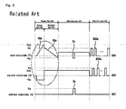
- FIG. 1 shows a structure of a prior art plasma display panel.
- the plasma display panel includes a front glass substrate 100 and a rear glass substrate 110 which are disposed in parallel to face each other at a given distance.
- a plurality of sustain electrode pairs in which a plurality of scan electrodes 102 and a plurality of sustain electrodes 103 are formed in pairs, are arranged on a front glass 101 of the front glass substrate 100 that is a display surface for displaying images.
- a plurality of address electrodes 113 are arranged on a rear glass 111 of the rear glass substrate 110 to intersect the plurality of sustain electrode pairs.
- the front glass substrate 100 includes the scan electrode 102 and the sustain electrode 103, which are discharged by each other in one discharge cell and sustain the light-emission of the cell.
- the scan electrode 102 and the sustain electrode 103 each include transparent electrodes 102a and 103a made of a transparent material and bus electrodes 102b and 103b made of a metal material such as Ag and made in pairs to form the sustain electrode pairs.
- the scan electrode 102 and the sustain electrode 103 limit the discharge current and are covered with one or more upper dielectric layers 104 to provide insulation between the sustain electrode pairs.
- a protective layer 105 formed by evaporating MgO is formed on upper surfaces of the dielectric layers 104 to facilitate discharge conditions.
- Stripe type (or well type) barrier ribs 112 are arranged in parallel in the rear glass substrate 110 to form a plurality of discharge spaces, that is, a plurality of discharge cells. Further, the plurality of address electrodes 113 which perform an address discharge to generate vacuum ultraviolet radiation are disposed in parallel with the barrier bibs 112. Red (R), green (G) and blue (B) phosphors 114 which emit visible light for the image display during the address discharge are coated on an upper surface of the rear glass substrate 110. A lower dielectric layer 115 for protecting the address electrodes 113 is formed between the address electrodes 113 and the phosphors 114.
- FIG. 2 A method of achieving gray scales in a plasma display panel is shown in FIG. 2.
- FIG. 2 shows a method of achieving gray scales in a related art plasma display panel.
- one frame is divided into several subfields whose number of light-emissions are different from one another.
- Each of the subfields includes a reset period for initializing all cells, an address period for selecting a cell to be discharged and a sustain period for realizing gray scale according to the durations of the discharges which are performed.
- a frame period (16.67 ms) corresponding to 1/60 sec is divided into eight subfields SF1 to SF8.
- the eight subfields SF1 to SF8 each includes a reset period, an address period and a sustain period.
- the duration of the reset period is the same as the duration of the address period for each of the subfields.
- the voltage difference between an address electrode and a transparent electrode which is a scan electrode generates an address discharge for selecting the cells to be discharged.
- n 0, 1, 2, 3, 4, 5, 6, 7
- a gray scale is realized by adjusting the sustain period of each of the subfields, that is, the number of times the sustain discharges are performed.
- a driving waveform according to a driving method of the plasma display panel is shown in FIG. 3.
- FIG. 3 shows a driving waveform according to a driving method of the prior art plasma display panel.
- the plasma display panel is driven by dividing into the reset period for initializing all the cells, the address period for selecting cells to be discharged, the sustain period for sustaining discharges of the selected cells and an erase period for erasing wall charges within the discharged cells.
- a rising waveform RUp is simultaneously applied to all of the scan electrodes during a setup period.
- a weak dark discharge is generated within the discharge cells of the entire screen by the rising waveform RUp.
- a falling waveform RDp which falls from a positive voltage lower than a peak voltage of the rising waveform RUp to a specific voltage of a ground level voltage or less is supplied to the cells to generate a weak erasure discharge within the cells.
- the weak erase discharge sufficiently erases the wall charges excessively accumulated on the scan electrode. By performing the setdown discharge, the wall charges uniformly remain within the cells to the degree that there is the generation of a stable address discharge.
- a negative scan pulse Sp is sequentially applied to the scan electrode and, at the same time, a positive data pulse Dp synchronized with the scan pulse Sp is applied to the address electrode. While the voltage difference between the negative scan pulse Sp and the positive data pulse Dp is added to the wall charges produced during the reset period, the address discharge is generated within the discharge cells to which the data pulse Dp is applied.
- the wall charges necessary for a discharge when applying a sustain voltage Vs are formed within the cells selected by the address discharge.
- a positive voltage Vz is supplied to the sustain electrode during the setdown period and the address period to decrease the voltage difference between the sustain electrode and the scan electrode, thereby preventing the discharge between the sustain electrode and the scan electrode from being generated.
- a sustain pulse SUSp is alternately supplied to the scan electrode and the sustain electrode. While the wall voltage within the cells selected by the address discharge is added to the sustain pulse SUSp, a sustain discharge, that is, a display discharge, is generated between the scan electrode and the sustain electrode whenever the sustain pulse SUSp is applied.
- the driving of one subfield of the plasma display panel is completed by the above-described processes.
- a high voltage of about 400 V or more is supplied as a setup voltage during the setup period to achieve uniformly the wall charges within the discharged cells.
- the supplying of high voltage to the plasma display panel can break down the insulating properties of the dielectric layer of the plasma display panel.
- the driving elements of the plasma display panel can be overload by the high voltage so that the driving elements of the plasma display apparatus must have a high-level withstanding voltage characteristic. This increases manufacturing costs of the plasma display apparatus. Further, there is a problem in that the driving efficiency of the plasma display apparatus is reduced.
- the present invention seeks to provide an improved plasma display apparatus.
- Embodiments of the present invention can provide a plasma display apparatus and a driving method thereof, which can lower a driving voltage when the plasma display apparatus is driven.
- a plasma display apparatus comprising a plasma display panel including a scan electrode and a sustain electrode, a scan driver arranged to apply a first pulse, which rises to a first voltage at a predetermined slope, to the scan electrode during a reset period, and a sustain driver arranged to apply a second pulse to the sustain electrode during the reset period for applying the first pulse to the scan electrode.
- a method of driving a plasma display apparatus comprising applying a first pulse, which rises from a ground level voltage to a first voltage at a predetermined slope, to a scan electrode during a reset period, and applying a second pulse having the opposite polarity of the polarity of the first pulse to a sustain electrode during the reset period for applying the first pulse to the scan electrode.
- a method of driving a plasma display apparatus comprising applying a first pulse, which rises to a first voltage at a predetermined slope, to a scan electrode during a reset period, and applying a second pulse, which falls at a predetermined slope, to a sustain electrode during the application of the first pulse to the scan electrode.
- a plasma display apparatus can be driven at a low voltage.
- driving elements of the plasma display apparatus do not need to have a high-level withstanding voltage characteristic capable of withstanding a high voltage, manufacturing costs can be reduced.
- a plasma display apparatus comprises a plasma display panel including a scan electrode and a sustain electrode, a scan driver arranged to apply a first pulse, which rises to a first voltage at a predetermined slope, to the scan electrode during a reset period, and a sustain driver arranged to apply a second pulse to the sustain electrode during the reset period for applying the first pulse to the scan electrode.
- a voltage of the first pulse may remain at the first voltage for a predetermined duration of time.
- the polarity of the first pulse may be different from the polarity of the second pulse.
- the polarity of the first pulse may be positive.
- the magnitude of the second pulse may be less than the magnitude of the first pulse.
- An absolute value of a voltage of the second pulse may be the same as a DC voltage supplied to the sustain electrode during an address period.
- An application time point of the second pulse may be substantially the same as an application time point of the first pulse.
- the application time point of the second pulse may be different from the application time point of the first pulse.
- the second pulse may be a sloped pulse.
- the second pulse may be a square wave.
- a method of driving a plasma display apparatus comprises applying a first pulse, which rises from a ground level voltage to a first voltage at a predetermined slope, to a scan electrode during a reset period, and applying a second pulse having the opposite polarity of the polarity of the first pulse to a sustain electrode during the reset period for applying the first pulse to the scan electrode.
- the second pulse may be a square wave.
- a method of driving a plasma display apparatus comprises applying a first pulse, which rises to a first voltage at a predetermined slope, to a scan electrode during a reset period, and applying a second pulse, which falls at a predetermined slope, to a sustain electrode during the application of the first pulse to the scan electrode.
- FIG. 1 shows a structure of a related art plasma display panel
- FIG. 2 shows a method of achieving gray scales in the related art plasma display panel
- FIG. 3 shows a driving waveform according to a driving method of the related art plasma display panel
- FIG. 4 shows a plasma display apparatus according to embodiments of the present invention
- FIG. 5 illustrates a driving method of a plasma display apparatus according to a first embodiment of the present invention
- FIG. 6 illustrates a driving method of a plasma display apparatus according to a second embodiment of the present invention.
- FIG. 7 illustrates a driving method of a plasma display apparatus according to a third embodiment of the present invention.
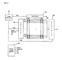
- a plasma display apparatus includes a plasma display panel 100, a data driver 122 for supplying data to address electrodes X1 to Xm formed on a lower substrate (not shown) of the plasma display panel 100, a scan driver 123 for driving scan electrodes Y1 to Yn, a sustain driver 124 for driving sustain electrodes Z being common electrodes, a timing controller 121 for controlling the data driver 122, the scan driver 123, the sustain driver 124 when the plasma display panel is driven, and a driving voltage generator 125 for supplying a necessary driving voltage to each of the drivers 122, 123 and 124.
- An upper substrate (not shown) and the lower substrate of the plasma display panel 100 are joined with each other at a given distance.
- a plurality of electrodes for example, the scan electrodes Y1 to Yn and the sustain electrodes Z are formed in pairs.
- the address electrodes X1 to Xm are formed to intersect the scan electrodes Y1 to Yn and the sustain electrodes Z.
- the data driver 122 receives data, which is inverse-gamma corrected and error diffused in an inverse gamma correction circuit (not shown) and an error diffusion circuit (not shown) and then mapped to each of the subfields in a subfield mapping circuit (not shown).
- the data is sampled and latched in response to a timing control signal CTRX from the timing controller 121 and then is supplied to the address electrodes X1 to Xm.
- the scan driver 123 supplies a first pulse, which rises to a first voltage Vst (refer to FIG. 5) at a predetermined slope, to the scan electrode during reset periods of one or more subfields of a plurality of subfields.
- the voltage of the scan electrode remains at the first voltage Vst for a predetermined duration of time and then perpendicularly falls to a second voltage Vs that is less than the first voltage Vst. Afterwards, a falling pulse, which falls at a predetermined slope, is supplied to the scan electrode.
- the reason why the voltage of the scan electrode remains at the first voltage Vst for the predetermined duration of time is to make the wall charges of the scan electrode uniform.
- the predetermined duration of time can be omitted to ensure a margin of driving timing.
- the scan driver 123 sequentially supplies a scan pulse of a scan voltage -Vy to the scan electrodes Y1 to Yn during an address period.
- the scan driver 123 supplies a sustain pulse, which is generated by an energy recovery circuit (not shown) installed in the scan driver 123, to the scan electrodes Y1 to Yn during a sustain period.
- the sustain driver 124 supplies a second pulse, which falls at a predetermined slope, or a square wave to the sustain electrodes Z during the reset periods of one or more subfields of the plurality of subfields, more specifically, during the supply of the first pulse to the scan electrode by the scan driver 123.
- the sustain driver 124 supplies a predetermined bias voltage Vzb (refer to FIG. 5) to the sustain electrodes Z during the address period.
- Vzb bias voltage
- an energy recovery circuit (not shown) installed in the sustain driver 124 and the energy recovery circuit (not shown) installed in the scan driver 123 are operated alternately to supply the sustain pulse to the sustain electrodes Z.
- the timing controller 121 receives a vertical/horizontal synchronization signal and a clock signal and generates timing control signals CTRX, CTRY and CTRZ for controlling operation timing and synchronization of each of the drivers 122, 123 and 124 in the reset period, the address period and the sustain period.
- the timing controller 121 supplies the timing control signals CTRX, CTRY and CTRZ to the corresponding drivers 122, 123 and 124 to control each of the drivers 122, 123 and 124.
- the data control signal CTRX includes a sampling clock for sampling data, a latch control signal, and a switch control signal for controlling an on/off time of a sustain driving circuit and a driving switch element.
- the scan control signal CTRY includes a switch control signal for controlling an on/off time of a sustain driving circuit and a driving switch element, which are installed in the scan driver 123.
- the sustain control signal CTRZ includes a switch control signal for controlling on/off time of a sustain driving circuit and a driving switch element, which are installed in the sustain driver 1 24.
- the driving voltage generator 125 generates a setup voltage Vsetup, a scan common voltage Vscan-com, a scan voltage -Vy, a sustain voltage Vs, and a data voltage Vd.
- the driving voltages can be varied depending on a composition of a discharge gas or a structure of the discharge cells.
- FIG. 5 illustrates a driving method of a plasma display apparatus according to a first embodiment.
- a plasma display apparatus is driven by dividing into a reset period for initializing all cells of a plasma display panel, an address period for selecting cells to be discharged and a sustain period for sustaining discharges of the selected cells.
- a first pulse rising to a first voltage Vst is simultaneously applied to all of the scan electrodes during a setup period.
- the first pulse is a positive pulse and a weak discharge is generated within all discharge cells of the plasma display panel by the first pulse. Due to the weak discharge, positive wall charges are accumulated on an address electrode X and a sustain electrode Z, negative wall charges are accumulated on a scan electrode Y.
- a reset voltage including a setup voltage which rises from a ground level voltage GND to the first voltage Vst at a predetermined slope, remains at the first voltage Vst for a predetermined duration of time and then perpendicularly falls to a second voltage Vs that is than the first voltage Vst, is applied to all the scan electrodes.
- a second pulse of polarity different from the polarity of the first pulse applied to the scan electrodes is applied to the sustain electrodes.
- the second pulse as shown by (a) and (b) in FIG. 5, is a square pulse or a falling pulse. The magnitude of a voltage of the second pulse is less than tha magnitude of the voltage of the first pulse.
- An absolute value of the voltage of the second pulse is the same as the magnitude of a positive DC voltage supplied to the sustain electrode during the address period which will be described later.
- the application time point of the second pulse applied to the sustain electrode is substantially the same as the application time point of the first pulse applied to the scan electrode.
- Positive charges are accumulated on the sustain electrode by an electrostatic affinity due to an electric field formed by applying the negative square pulse voltage -Vz.
- a falling pulse is applied to the scan electrode and a positive DC voltage Vzb is supplied to the sustain electrode so that wall charges necessary for a stable address discharge during the address period uniformly remain within the cells.
- a positive data pulse Dp and a negative scan pulse Sp are applied to the address electrode and the scan electrode in synchronous with each other, respectively. While the voltage difference between the address electrode and the scan electrode is added to the wall voltage between the address electrode and the scan electrode caused by the wall charges formed during the reset period, the address discharge is generated.
- a large amount of the positive wall charges are accumulated on the sustain electrode during the reset period for the next address discharge.
- a stabe address discharge can be generated during the address period without applying a high voltage to the scan electrode in the reset period.
- a sufficient driving margin of the plasma display apparatus can be obtained by increasing the driving efficiency of the plasma display apparatus.
- the positive voltage Vzb is supplied to the sustain electrode during the address period to decrease the voltage difference between the sustain electrode and the scan electrode during the setdown period and the address period, thereby preventing generation of the discharge between the sustain electrode and the scan electrode.
- a sustain pulse SUSp is alternately applied to the scan electrode and the sustain electrode. While the wall voltages within the cells selected by the address discharge are added to the sustain pulse SUSp, a sustain discharge, that is, a display discharge, is generated between the scan electrode and the sustain electrode whenever the sustain pulse SUSp is applied.
- the driving method of the plasma display apparatus according to the second and third embodiments shown in FIGS. 6 and 7 is almost the same as the driving method of the plasma display apparatus according to the first embodiment shown in FIG. 5.
- the application time point of a second pulse applied to a sustain electrode is different from the application time point of a first pulse applied to a scan electrode during a reset period.
- the application time point of the second pulse applied to the sustain electrode is earlier than the application time point of the first pulse applied to the scan electrode.
- An amount of time corresponding to the difference between the application time point of the second pulse and the application time point of the first pulse is less than 1/5 of the total amount of time of the setup period. If the amount of time is longer than 1/5, the potential difference between the scan electrode and the sustain electrode is not enough to generate a reset discharge during a reset period.
- the application time point of the second pulse applied to the sustain electrode is later than the application time point of the first pulse applied to the scan electrode.
- An amount of time corresponding to the difference between the application time points of the second pulse and the first pulse is less than 1/5 of the total amount of time of the setup period. Since the reason is the same as that of the second embodiment, the description thereof is omitted.
Abstract
Description
- This invention relates to a display apparatus. It more particularly relates to a plasma display apparatus and a driving method thereof.
- A plasma display apparatus is one of various kinds of display apparatuses, and generally includes a plasma display panel and a driver for driving the plasma display panel.
- Barrier ribs are formed between a front glass substrate and a rear glass substrate of the plasma display panel to form a unit cell. Each cell is filled with a main discharge gas such as neon (Ne), helium (He) or a Ne-He gas mixture and an inert gas containing a small amount of xenon (Xe). When the plasma display panel is discharged by a high frequency voltage, the inert gas generates vacuum ultraviolet radiation and phosphors formed between the barrier ribs are stimulated to emit visible light by the vacuum ultraviolet radiation. By these processes, a visible image is produced.
- FIG. 1 shows a structure of a prior art plasma display panel.
- As shown in FIG. 1, the plasma display panel includes a
front glass substrate 100 and arear glass substrate 110 which are disposed in parallel to face each other at a given distance. A plurality of sustain electrode pairs, in which a plurality ofscan electrodes 102 and a plurality ofsustain electrodes 103 are formed in pairs, are arranged on afront glass 101 of thefront glass substrate 100 that is a display surface for displaying images. A plurality ofaddress electrodes 113 are arranged on a rear glass 111 of therear glass substrate 110 to intersect the plurality of sustain electrode pairs. - The
front glass substrate 100 includes thescan electrode 102 and thesustain electrode 103, which are discharged by each other in one discharge cell and sustain the light-emission of the cell. Thescan electrode 102 and thesustain electrode 103 each include transparent electrodes 102a and 103a made of a transparent material and bus electrodes 102b and 103b made of a metal material such as Ag and made in pairs to form the sustain electrode pairs. Thescan electrode 102 and thesustain electrode 103 limit the discharge current and are covered with one or more upperdielectric layers 104 to provide insulation between the sustain electrode pairs. Aprotective layer 105 formed by evaporating MgO is formed on upper surfaces of thedielectric layers 104 to facilitate discharge conditions. - Stripe type (or well type)
barrier ribs 112 are arranged in parallel in therear glass substrate 110 to form a plurality of discharge spaces, that is, a plurality of discharge cells. Further, the plurality ofaddress electrodes 113 which perform an address discharge to generate vacuum ultraviolet radiation are disposed in parallel with thebarrier bibs 112. Red (R), green (G) and blue (B)phosphors 114 which emit visible light for the image display during the address discharge are coated on an upper surface of therear glass substrate 110. A lowerdielectric layer 115 for protecting theaddress electrodes 113 is formed between theaddress electrodes 113 and thephosphors 114. - A method of achieving gray scales in a plasma display panel is shown in FIG. 2.
- FIG. 2 shows a method of achieving gray scales in a related art plasma display panel.
- As shown in FIG. 2, in the plasma display panel, one frame is divided into several subfields whose number of light-emissions are different from one another. Each of the subfields includes a reset period for initializing all cells, an address period for selecting a cell to be discharged and a sustain period for realizing gray scale according to the durations of the discharges which are performed. For example, in a case of realizing 256 level gray scale, a frame period (16.67 ms) corresponding to 1/60 sec, as shown in FIG. 2 is divided into eight subfields SF1 to SF8. The eight subfields SF1 to SF8 each includes a reset period, an address period and a sustain period.
- The duration of the reset period is the same as the duration of the address period for each of the subfields. The voltage difference between an address electrode and a transparent electrode which is a scan electrode generates an address discharge for selecting the cells to be discharged. The sustain period increases in a ratio of 2n (n = 0, 1, 2, 3, 4, 5, 6, 7) at each of the subfields. As described above, since the sustain period changes according to weight values of the subfields, a gray scale is realized by adjusting the sustain period of each of the subfields, that is, the number of times the sustain discharges are performed. A driving waveform according to a driving method of the plasma display panel is shown in FIG. 3.
- FIG. 3 shows a driving waveform according to a driving method of the prior art plasma display panel.
- As shown in FIG. 3, the plasma display panel is driven by dividing into the reset period for initializing all the cells, the address period for selecting cells to be discharged, the sustain period for sustaining discharges of the selected cells and an erase period for erasing wall charges within the discharged cells.
- In the reset period, a rising waveform RUp is simultaneously applied to all of the scan electrodes during a setup period. A weak dark discharge is generated within the discharge cells of the entire screen by the rising waveform RUp. By performing the setup discharge, positive wall charges are accumulated on the address electrode and the sustain electrode and negative wall charges are accumulated on the scan electrode.
- In a setdown period, after the rising waveform RUp is supplied during the setup period, a falling waveform RDp which falls from a positive voltage lower than a peak voltage of the rising waveform RUp to a specific voltage of a ground level voltage or less is supplied to the cells to generate a weak erasure discharge within the cells. The weak erase discharge sufficiently erases the wall charges excessively accumulated on the scan electrode. By performing the setdown discharge, the wall charges uniformly remain within the cells to the degree that there is the generation of a stable address discharge.
- In the address period, a negative scan pulse Sp is sequentially applied to the scan electrode and, at the same time, a positive data pulse Dp synchronized with the scan pulse Sp is applied to the address electrode. While the voltage difference between the negative scan pulse Sp and the positive data pulse Dp is added to the wall charges produced during the reset period, the address discharge is generated within the discharge cells to which the data pulse Dp is applied. The wall charges necessary for a discharge when applying a sustain voltage Vs are formed within the cells selected by the address discharge. A positive voltage Vz is supplied to the sustain electrode during the setdown period and the address period to decrease the voltage difference between the sustain electrode and the scan electrode, thereby preventing the discharge between the sustain electrode and the scan electrode from being generated.
- In the sustain period, a sustain pulse SUSp is alternately supplied to the scan electrode and the sustain electrode. While the wall voltage within the cells selected by the address discharge is added to the sustain pulse SUSp, a sustain discharge, that is, a display discharge, is generated between the scan electrode and the sustain electrode whenever the sustain pulse SUSp is applied.
- The driving of one subfield of the plasma display panel is completed by the above-described processes.
- In the prior art driving method of the plasma display panel as described above, a high voltage of about 400 V or more is supplied as a setup voltage during the setup period to achieve uniformly the wall charges within the discharged cells.
- The supplying of high voltage to the plasma display panel can break down the insulating properties of the dielectric layer of the plasma display panel.
- Further, the driving elements of the plasma display panel can be overload by the high voltage so that the driving elements of the plasma display apparatus must have a high-level withstanding voltage characteristic. This increases manufacturing costs of the plasma display apparatus. Further, there is a problem in that the driving efficiency of the plasma display apparatus is reduced.
- The present invention seeks to provide an improved plasma display apparatus.
- Embodiments of the present invention can provide a plasma display apparatus and a driving method thereof, which can lower a driving voltage when the plasma display apparatus is driven.
- In accordance with a first aspect of the invention, there is provided a plasma display apparatus comprising a plasma display panel including a scan electrode and a sustain electrode, a scan driver arranged to apply a first pulse, which rises to a first voltage at a predetermined slope, to the scan electrode during a reset period, and a sustain driver arranged to apply a second pulse to the sustain electrode during the reset period for applying the first pulse to the scan electrode.
- According to another aspect of the invention, there is provided a method of driving a plasma display apparatus comprising applying a first pulse, which rises from a ground level voltage to a first voltage at a predetermined slope, to a scan electrode during a reset period, and applying a second pulse having the opposite polarity of the polarity of the first pulse to a sustain electrode during the reset period for applying the first pulse to the scan electrode.
- According to still another aspect of the present invention, there is provided a method of driving a plasma display apparatus comprising applying a first pulse, which rises to a first voltage at a predetermined slope, to a scan electrode during a reset period, and applying a second pulse, which falls at a predetermined slope, to a sustain electrode during the application of the first pulse to the scan electrode.
- A plasma display apparatus according to embodiments of the invention can be driven at a low voltage.
- Further, since driving elements of the plasma display apparatus do not need to have a high-level withstanding voltage characteristic capable of withstanding a high voltage, manufacturing costs can be reduced.
- In accordance with another aspect of the invention, a plasma display apparatus comprises a plasma display panel including a scan electrode and a sustain electrode, a scan driver arranged to apply a first pulse, which rises to a first voltage at a predetermined slope, to the scan electrode during a reset period, and a sustain driver arranged to apply a second pulse to the sustain electrode during the reset period for applying the first pulse to the scan electrode.
- A voltage of the first pulse may remain at the first voltage for a predetermined duration of time.
- The polarity of the first pulse may be different from the polarity of the second pulse.
- The polarity of the first pulse may be positive.
- The magnitude of the second pulse may be less than the magnitude of the first pulse.
- An absolute value of a voltage of the second pulse may be the same as a DC voltage supplied to the sustain electrode during an address period.
- An application time point of the second pulse may be substantially the same as an application time point of the first pulse.
- The application time point of the second pulse may be different from the application time point of the first pulse.
- The second pulse may be a sloped pulse.
- The second pulse may be a square wave.
- In accordance with another aspect of the invention, a method of driving a plasma display apparatus comprises applying a first pulse, which rises from a ground level voltage to a first voltage at a predetermined slope, to a scan electrode during a reset period, and applying a second pulse having the opposite polarity of the polarity of the first pulse to a sustain electrode during the reset period for applying the first pulse to the scan electrode.
- The second pulse may be a square wave.
- In accordance with another aspect of the invention, a method of driving a plasma display apparatus comprises applying a first pulse, which rises to a first voltage at a predetermined slope, to a scan electrode during a reset period, and applying a second pulse, which falls at a predetermined slope, to a sustain electrode during the application of the first pulse to the scan electrode.
- Embodiments of the invention will now be described by way of nonlimiting example only, with referene to the drawings, in which:
- FIG. 1 shows a structure of a related art plasma display panel;
- FIG. 2 shows a method of achieving gray scales in the related art plasma display panel;
- FIG. 3 shows a driving waveform according to a driving method of the related art plasma display panel;
- FIG. 4 shows a plasma display apparatus according to embodiments of the present invention;
- FIG. 5 illustrates a driving method of a plasma display apparatus according to a first embodiment of the present invention;
- FIG. 6 illustrates a driving method of a plasma display apparatus according to a second embodiment of the present invention; and
- FIG. 7 illustrates a driving method of a plasma display apparatus according to a third embodiment of the present invention.
- As shown in FIG. 4, a plasma display apparatus includes a
plasma display panel 100, adata driver 122 for supplying data to address electrodes X1 to Xm formed on a lower substrate (not shown) of theplasma display panel 100, ascan driver 123 for driving scan electrodes Y1 to Yn, a sustaindriver 124 for driving sustain electrodes Z being common electrodes, atiming controller 121 for controlling thedata driver 122, thescan driver 123, the sustaindriver 124 when the plasma display panel is driven, and a drivingvoltage generator 125 for supplying a necessary driving voltage to each of thedrivers - An upper substrate (not shown) and the lower substrate of the
plasma display panel 100 are joined with each other at a given distance. On the upper substrate, a plurality of electrodes, for example, the scan electrodes Y1 to Yn and the sustain electrodes Z are formed in pairs. On the lower substrate, the address electrodes X1 to Xm are formed to intersect the scan electrodes Y1 to Yn and the sustain electrodes Z. - The
data driver 122 receives data, which is inverse-gamma corrected and error diffused in an inverse gamma correction circuit (not shown) and an error diffusion circuit (not shown) and then mapped to each of the subfields in a subfield mapping circuit (not shown). In thedata driver 122, the data is sampled and latched in response to a timing control signal CTRX from thetiming controller 121 and then is supplied to the address electrodes X1 to Xm. - Under the control of the
timing controller 121, thescan driver 123 supplies a first pulse, which rises to a first voltage Vst (refer to FIG. 5) at a predetermined slope, to the scan electrode during reset periods of one or more subfields of a plurality of subfields. The voltage of the scan electrode remains at the first voltage Vst for a predetermined duration of time and then perpendicularly falls to a second voltage Vs that is less than the first voltage Vst. Afterwards, a falling pulse, which falls at a predetermined slope, is supplied to the scan electrode. - The reason why the voltage of the scan electrode remains at the first voltage Vst for the predetermined duration of time is to make the wall charges of the scan electrode uniform. However, the predetermined duration of time can be omitted to ensure a margin of driving timing.
- Under the control of the
timing controller 121, thescan driver 123 sequentially supplies a scan pulse of a scan voltage -Vy to the scan electrodes Y1 to Yn during an address period. Thescan driver 123 supplies a sustain pulse, which is generated by an energy recovery circuit (not shown) installed in thescan driver 123, to the scan electrodes Y1 to Yn during a sustain period. - Under the control of the
timing controller 121, the sustaindriver 124 supplies a second pulse, which falls at a predetermined slope, or a square wave to the sustain electrodes Z during the reset periods of one or more subfields of the plurality of subfields, more specifically, during the supply of the first pulse to the scan electrode by thescan driver 123. The sustaindriver 124 supplies a predetermined bias voltage Vzb (refer to FIG. 5) to the sustain electrodes Z during the address period. During the sustain period, an energy recovery circuit (not shown) installed in the sustaindriver 124 and the energy recovery circuit (not shown) installed in thescan driver 123 are operated alternately to supply the sustain pulse to the sustain electrodes Z. - The
timing controller 121 receives a vertical/horizontal synchronization signal and a clock signal and generates timing control signals CTRX, CTRY and CTRZ for controlling operation timing and synchronization of each of thedrivers timing controller 121 supplies the timing control signals CTRX, CTRY and CTRZ to the correspondingdrivers drivers - The data control signal CTRX includes a sampling clock for sampling data, a latch control signal, and a switch control signal for controlling an on/off time of a sustain driving circuit and a driving switch element. The scan control signal CTRY includes a switch control signal for controlling an on/off time of a sustain driving circuit and a driving switch element, which are installed in the
scan driver 123. The sustain control signal CTRZ includes a switch control signal for controlling on/off time of a sustain driving circuit and a driving switch element, which are installed in the sustaindriver 1 24. - The driving
voltage generator 125 generates a setup voltage Vsetup, a scan common voltage Vscan-com, a scan voltage -Vy, a sustain voltage Vs, and a data voltage Vd. The driving voltages can be varied depending on a composition of a discharge gas or a structure of the discharge cells. - FIG. 5 illustrates a driving method of a plasma display apparatus according to a first embodiment.
- As shown in FIG. 5, a plasma display apparatus is driven by dividing into a reset period for initializing all cells of a plasma display panel, an address period for selecting cells to be discharged and a sustain period for sustaining discharges of the selected cells.
- In the reset period, a first pulse rising to a first voltage Vst is simultaneously applied to all of the scan electrodes during a setup period. The first pulse is a positive pulse and a weak discharge is generated within all discharge cells of the plasma display panel by the first pulse. Due to the weak discharge, positive wall charges are accumulated on an address electrode X and a sustain electrode Z, negative wall charges are accumulated on a scan electrode Y.
- During the setup period, a reset voltage including a setup voltage, which rises from a ground level voltage GND to the first voltage Vst at a predetermined slope, remains at the first voltage Vst for a predetermined duration of time and then perpendicularly falls to a second voltage Vs that is than the first voltage Vst, is applied to all the scan electrodes. A second pulse of polarity different from the polarity of the first pulse applied to the scan electrodes is applied to the sustain electrodes. The second pulse, as shown by (a) and (b) in FIG. 5, is a square pulse or a falling pulse. The magnitude of a voltage of the second pulse is less than tha magnitude of the voltage of the first pulse.
- An absolute value of the voltage of the second pulse is the same as the magnitude of a positive DC voltage supplied to the sustain electrode during the address period which will be described later.
- The application time point of the second pulse applied to the sustain electrode is substantially the same as the application time point of the first pulse applied to the scan electrode.
- Positive charges are accumulated on the sustain electrode by an electrostatic affinity due to an electric field formed by applying the negative square pulse voltage -Vz.
- In a setdown period, a falling pulse is applied to the scan electrode and a positive DC voltage Vzb is supplied to the sustain electrode so that wall charges necessary for a stable address discharge during the address period uniformly remain within the cells.
- In the address period, a positive data pulse Dp and a negative scan pulse Sp are applied to the address electrode and the scan electrode in synchronous with each other, respectively. While the voltage difference between the address electrode and the scan electrode is added to the wall voltage between the address electrode and the scan electrode caused by the wall charges formed during the reset period, the address discharge is generated.
- As described above, a large amount of the positive wall charges are accumulated on the sustain electrode during the reset period for the next address discharge. As a result, a stabe address discharge can be generated during the address period without applying a high voltage to the scan electrode in the reset period. Further, a sufficient driving margin of the plasma display apparatus can be obtained by increasing the driving efficiency of the plasma display apparatus.
- The positive voltage Vzb is supplied to the sustain electrode during the address period to decrease the voltage difference between the sustain electrode and the scan electrode during the setdown period and the address period, thereby preventing generation of the discharge between the sustain electrode and the scan electrode.
- In the sustain period, a sustain pulse SUSp is alternately applied to the scan electrode and the sustain electrode. While the wall voltages within the cells selected by the address discharge are added to the sustain pulse SUSp, a sustain discharge, that is, a display discharge, is generated between the scan electrode and the sustain electrode whenever the sustain pulse SUSp is applied.
- The driving method of the plasma display apparatus according to the second and third embodiments shown in FIGS. 6 and 7 is almost the same as the driving method of the plasma display apparatus according to the first embodiment shown in FIG. 5. However, the application time point of a second pulse applied to a sustain electrode is different from the application time point of a first pulse applied to a scan electrode during a reset period.
- As shown in FIG. 6, the application time point of the second pulse applied to the sustain electrode is earlier than the application time point of the first pulse applied to the scan electrode. An amount of time corresponding to the difference between the application time point of the second pulse and the application time point of the first pulse is less than 1/5 of the total amount of time of the setup period. If the amount of time is longer than 1/5, the potential difference between the scan electrode and the sustain electrode is not enough to generate a reset discharge during a reset period.
- As shown in FIG. 7, contrary to FIG. 6, the application time point of the second pulse applied to the sustain electrode is later than the application time point of the first pulse applied to the scan electrode. An amount of time corresponding to the difference between the application time points of the second pulse and the first pulse is less than 1/5 of the total amount of time of the setup period. Since the reason is the same as that of the second embodiment, the description thereof is omitted.
- As described above, if the application time point of the first pulse applied to the scan electrode is different from the application time point of the second pulse applied to the sustain electrode in the reset period, a displacement current generated between the scan electrode and the sustain electrode, which are next to each other, decreases so that pulse noise will decrease.
- It will be apparent to those skilled in the art that various modifications and variation can be made in the present invention without departing from the scope of the invention. Thus, it is intended that the present invention cover the modifications and variations of this invention provided they come within the scope of the claims and their equivalents.
Claims (15)
- A plasma display apparatus comprising:a plasma display panel including a scan electrode and a sustain electrode;a scan driver arranged to apply a first pulse, which rises to a first voltage at a predetermined slope, to the scan electrode during a reset period; anda sustain driver arranged to apply a second pulse to the sustain electrode during the reset period.
- The plasma display apparatus as claimed in claim 1, wherein the voltage of the first pulse remains at the first voltage for a predetermined duration of time.
- The plasma display apparatus as claimed in claim 1, wherein the polarity of the first pulse is different from the polarity of the second pulse.
- The plasma display apparatus as claimed in claim 3, wherein the polarity of the first pulse is positive.
- The plasma display apparatus as claimed in claim 1, wherein the magnitude of the second pulse is less than the magnitude of the first pulse.
- The plasma display apparatus as claimed in claim 1, wherein the absolute value of a voltage of the second pulse is the same as the DC voltage supplied to the sustain electrode during an address period.
- The plasma display apparatus as claimed in claim 1, wherein the application time point of the second pulse is substantially the same as the application time point of the first pulse.
- The plasma display apparatus as claimed in claim 1, wherein the application time point of the second pulse is different from the application time point of the first pulse.
- The plasma display apparatus as claimed in claim 1, wherein the second pulse is a sloped pulse or a square wave.
- A method of driving a plasma display apparatus comprising:applying a first pulse, which rises to a first voltage at a predetermined slope, to a scan electrode during a reset period; andapplying a second pulse, which falls at a predetermined slope, to a sustain electrode during the application of the first pulse to the scan electrode.
- The method as claimed in claim 10, wherein the voltage of the first pulse remains at the first voltage during a predetermined duration of time.
- The method as claimed in claim 10, wherein the polarity of the first pulse is different from the polarity of the second pulse.
- The method as claimed in claim 10, wherein the magnitude of the second pulse is less than the magnitude of the first pulse.
- The method as claimed in claim 10, wherein the application time point of the second pulse is substantially the same as the application time point of the first pulse.
- The method as claimed in claim 10, wherein the application time point of the second pulse is different from the application time point of the first pulse.
Applications Claiming Priority (1)
| Application Number | Priority Date | Filing Date | Title |
|---|---|---|---|
| KR1020050001413A KR20060080825A (en) | 2005-01-06 | 2005-01-06 | Driving method and apparatus for plasma display panel |
Publications (1)
| Publication Number | Publication Date |
|---|---|
| EP1679686A1 true EP1679686A1 (en) | 2006-07-12 |
Family
ID=36123212
Family Applications (1)
| Application Number | Title | Priority Date | Filing Date |
|---|---|---|---|
| EP06250027A Withdrawn EP1679686A1 (en) | 2005-01-06 | 2006-01-05 | Plasma display apparatus and driving method thereof |
Country Status (4)
| Country | Link |
|---|---|
| US (1) | US20070205966A1 (en) |
| EP (1) | EP1679686A1 (en) |
| KR (1) | KR20060080825A (en) |
| CN (1) | CN1801276A (en) |
Families Citing this family (2)
| Publication number | Priority date | Publication date | Assignee | Title |
|---|---|---|---|---|
| KR100877819B1 (en) * | 2006-11-07 | 2009-01-12 | 엘지전자 주식회사 | Plasma Display Apparatus |
| KR20080092749A (en) * | 2007-04-13 | 2008-10-16 | 엘지전자 주식회사 | Plasma display apparatus |
Citations (5)
| Publication number | Priority date | Publication date | Assignee | Title |
|---|---|---|---|---|
| US20020067321A1 (en) | 2000-06-22 | 2002-06-06 | Yoshikazu Kanazawa | Plasma display panel and method of driving the same capable of providing high definition and high aperture ratio |
| US20020118149A1 (en) * | 2001-02-27 | 2002-08-29 | Nec Corporation | Method of driving plasma display panel |
| EP1271462A2 (en) * | 2001-06-29 | 2003-01-02 | Fujitsu Limited | Method and device for driving an alternating current plasma display panel |
| US20030095083A1 (en) | 2001-11-22 | 2003-05-22 | Nec Plasma Display Corporation | AC-Type plasma display panel and method for driving same |
| US20040189549A1 (en) * | 2003-03-31 | 2004-09-30 | Fujitsu Limited | Method for driving plasma display panel |
Family Cites Families (6)
| Publication number | Priority date | Publication date | Assignee | Title |
|---|---|---|---|---|
| US6653795B2 (en) * | 2000-03-14 | 2003-11-25 | Lg Electronics Inc. | Method and apparatus for driving plasma display panel using selective writing and selective erasure |
| JP4357107B2 (en) * | 2000-10-05 | 2009-11-04 | 日立プラズマディスプレイ株式会社 | Driving method of plasma display |
| JP3573705B2 (en) * | 2000-11-07 | 2004-10-06 | 富士通日立プラズマディスプレイ株式会社 | Plasma display panel and driving method thereof |
| JP2004004513A (en) * | 2002-04-25 | 2004-01-08 | Fujitsu Hitachi Plasma Display Ltd | Driving method for plasma display panel, and plasma display device |
| JP2003345292A (en) * | 2002-05-24 | 2003-12-03 | Fujitsu Hitachi Plasma Display Ltd | Method for driving plasma display panel |
| KR100536249B1 (en) * | 2003-10-24 | 2005-12-12 | 삼성에스디아이 주식회사 | A plasma display panel, a driving apparatus and a driving method of the same |
-
2005
- 2005-01-06 KR KR1020050001413A patent/KR20060080825A/en not_active Application Discontinuation
-
2006
- 2006-01-04 US US11/275,450 patent/US20070205966A1/en not_active Abandoned
- 2006-01-05 EP EP06250027A patent/EP1679686A1/en not_active Withdrawn
- 2006-01-06 CN CNA2006100057537A patent/CN1801276A/en active Pending
Patent Citations (5)
| Publication number | Priority date | Publication date | Assignee | Title |
|---|---|---|---|---|
| US20020067321A1 (en) | 2000-06-22 | 2002-06-06 | Yoshikazu Kanazawa | Plasma display panel and method of driving the same capable of providing high definition and high aperture ratio |
| US20020118149A1 (en) * | 2001-02-27 | 2002-08-29 | Nec Corporation | Method of driving plasma display panel |
| EP1271462A2 (en) * | 2001-06-29 | 2003-01-02 | Fujitsu Limited | Method and device for driving an alternating current plasma display panel |
| US20030095083A1 (en) | 2001-11-22 | 2003-05-22 | Nec Plasma Display Corporation | AC-Type plasma display panel and method for driving same |
| US20040189549A1 (en) * | 2003-03-31 | 2004-09-30 | Fujitsu Limited | Method for driving plasma display panel |
Also Published As
| Publication number | Publication date |
|---|---|
| KR20060080825A (en) | 2006-07-11 |
| US20070205966A1 (en) | 2007-09-06 |
| CN1801276A (en) | 2006-07-12 |
Similar Documents
| Publication | Publication Date | Title |
|---|---|---|
| EP1736956A1 (en) | Plasma display apparatrus and method of driving the same | |
| EP1785977B1 (en) | Plasma display apparatus | |
| JP2006189847A (en) | Plasma display apparatus and driving method thereof | |
| EP1693820A1 (en) | Plasma display apparatus and driving method thereof | |
| JP4253647B2 (en) | Plasma display panel driving apparatus and method | |
| KR100784543B1 (en) | Plasma Display Apparatus and Driving Method thereof | |
| EP1713052A2 (en) | Plasma display apparatus, plasma display panel, and driving device and method thereof | |
| JP2006011459A5 (en) | ||
| EP1770678A2 (en) | Plasma display apparatus and driving method thereof | |
| EP1679686A1 (en) | Plasma display apparatus and driving method thereof | |
| EP1775697A2 (en) | Plasma display apparatus | |
| EP1669973A2 (en) | Plasma display apparatus | |
| KR100747269B1 (en) | Plasma Display Apparatus and Driving Method thereof | |
| US7889155B2 (en) | Plasma display apparatus | |
| KR20070087743A (en) | Plasma display apparatus and driving method thereof | |
| KR100681018B1 (en) | Plasma display apparatus and driving method thereof | |
| KR100658357B1 (en) | Plasma display apparatus and driving method thereof | |
| EP1939843A1 (en) | Plasma display apparatus and driving method thereof | |
| EP1669971A1 (en) | Plasma display apparatus and driving method thereof | |
| US20080055204A1 (en) | Plasma display apparatus and method of driving the same | |
| KR100658343B1 (en) | Plasma display apparatus and driving method thereof | |
| KR100705280B1 (en) | Plasma Display Apparatus and Driving Method thereof | |
| KR100747206B1 (en) | Plasma Display Apparatus and Driving Method thereof | |
| KR100646319B1 (en) | Plasma Display Apparatus and Driving Method thereof | |
| KR100692868B1 (en) | Plasma display Apparatus and driving method thereof |
Legal Events
| Date | Code | Title | Description |
|---|---|---|---|
| PUAI | Public reference made under article 153(3) epc to a published international application that has entered the european phase |
Free format text: ORIGINAL CODE: 0009012 |
|
| 17P | Request for examination filed |
Effective date: 20060118 |
|
| AK | Designated contracting states |
Kind code of ref document: A1 Designated state(s): AT BE BG CH CY CZ DE DK EE ES FI FR GB GR HU IE IS IT LI LT LU LV MC NL PL PT RO SE SI SK TR |
|
| AX | Request for extension of the european patent |
Extension state: AL BA HR MK YU |
|
| AKX | Designation fees paid |
Designated state(s): DE FR GB NL |
|
| 17Q | First examination report despatched |
Effective date: 20070601 |
|
| STAA | Information on the status of an ep patent application or granted ep patent |
Free format text: STATUS: THE APPLICATION IS DEEMED TO BE WITHDRAWN |
|
| 18D | Application deemed to be withdrawn |
Effective date: 20100721 |