EP1784065A1 - Electrode substrate - Google Patents
Electrode substrate Download PDFInfo
- Publication number
- EP1784065A1 EP1784065A1 EP05770814A EP05770814A EP1784065A1 EP 1784065 A1 EP1784065 A1 EP 1784065A1 EP 05770814 A EP05770814 A EP 05770814A EP 05770814 A EP05770814 A EP 05770814A EP 1784065 A1 EP1784065 A1 EP 1784065A1
- Authority
- EP
- European Patent Office
- Prior art keywords
- electrodes
- electrode
- wiring board
- substrate
- electronic
- Prior art date
- Legal status (The legal status is an assumption and is not a legal conclusion. Google has not performed a legal analysis and makes no representation as to the accuracy of the status listed.)
- Ceased
Links
Images






Classifications
-
- H—ELECTRICITY
- H05—ELECTRIC TECHNIQUES NOT OTHERWISE PROVIDED FOR
- H05K—PRINTED CIRCUITS; CASINGS OR CONSTRUCTIONAL DETAILS OF ELECTRIC APPARATUS; MANUFACTURE OF ASSEMBLAGES OF ELECTRICAL COMPONENTS
- H05K3/00—Apparatus or processes for manufacturing printed circuits
- H05K3/22—Secondary treatment of printed circuits
- H05K3/24—Reinforcing of the conductive pattern
- H05K3/243—Reinforcing of the conductive pattern characterised by selective plating, e.g. for finish plating of pads
-
- H—ELECTRICITY
- H10—SEMICONDUCTOR DEVICES; ELECTRIC SOLID-STATE DEVICES NOT OTHERWISE PROVIDED FOR
- H10W—GENERIC PACKAGES, INTERCONNECTIONS, CONNECTORS OR OTHER CONSTRUCTIONAL DETAILS OF DEVICES COVERED BY CLASS H10
- H10W70/00—Package substrates; Interposers; Redistribution layers [RDL]
- H10W70/01—Manufacture or treatment
- H10W70/05—Manufacture or treatment of insulating or insulated package substrates, or of interposers, or of redistribution layers
- H10W70/098—Applying pastes or inks, e.g. screen printing
-
- H—ELECTRICITY
- H10—SEMICONDUCTOR DEVICES; ELECTRIC SOLID-STATE DEVICES NOT OTHERWISE PROVIDED FOR
- H10W—GENERIC PACKAGES, INTERCONNECTIONS, CONNECTORS OR OTHER CONSTRUCTIONAL DETAILS OF DEVICES COVERED BY CLASS H10
- H10W70/00—Package substrates; Interposers; Redistribution layers [RDL]
- H10W70/60—Insulating or insulated package substrates; Interposers; Redistribution layers
-
- H—ELECTRICITY
- H10—SEMICONDUCTOR DEVICES; ELECTRIC SOLID-STATE DEVICES NOT OTHERWISE PROVIDED FOR
- H10W—GENERIC PACKAGES, INTERCONNECTIONS, CONNECTORS OR OTHER CONSTRUCTIONAL DETAILS OF DEVICES COVERED BY CLASS H10
- H10W70/00—Package substrates; Interposers; Redistribution layers [RDL]
- H10W70/60—Insulating or insulated package substrates; Interposers; Redistribution layers
- H10W70/67—Insulating or insulated package substrates; Interposers; Redistribution layers characterised by their insulating layers or insulating parts
- H10W70/69—Insulating materials thereof
-
- H—ELECTRICITY
- H10—SEMICONDUCTOR DEVICES; ELECTRIC SOLID-STATE DEVICES NOT OTHERWISE PROVIDED FOR
- H10W—GENERIC PACKAGES, INTERCONNECTIONS, CONNECTORS OR OTHER CONSTRUCTIONAL DETAILS OF DEVICES COVERED BY CLASS H10
- H10W74/00—Encapsulations, e.g. protective coatings
- H10W74/01—Manufacture or treatment
- H10W74/012—Manufacture or treatment of encapsulations on active surfaces of flip-chip devices, e.g. forming underfills
-
- H—ELECTRICITY
- H10—SEMICONDUCTOR DEVICES; ELECTRIC SOLID-STATE DEVICES NOT OTHERWISE PROVIDED FOR
- H10W—GENERIC PACKAGES, INTERCONNECTIONS, CONNECTORS OR OTHER CONSTRUCTIONAL DETAILS OF DEVICES COVERED BY CLASS H10
- H10W74/00—Encapsulations, e.g. protective coatings
- H10W74/10—Encapsulations, e.g. protective coatings characterised by their shape or disposition
- H10W74/15—Encapsulations, e.g. protective coatings characterised by their shape or disposition on active surfaces of flip-chip devices, e.g. underfills
-
- H—ELECTRICITY
- H05—ELECTRIC TECHNIQUES NOT OTHERWISE PROVIDED FOR
- H05K—PRINTED CIRCUITS; CASINGS OR CONSTRUCTIONAL DETAILS OF ELECTRIC APPARATUS; MANUFACTURE OF ASSEMBLAGES OF ELECTRICAL COMPONENTS
- H05K1/00—Printed circuits
- H05K1/02—Details
- H05K1/0266—Marks, test patterns or identification means
- H05K1/0268—Marks, test patterns or identification means for electrical inspection or testing
-
- H—ELECTRICITY
- H05—ELECTRIC TECHNIQUES NOT OTHERWISE PROVIDED FOR
- H05K—PRINTED CIRCUITS; CASINGS OR CONSTRUCTIONAL DETAILS OF ELECTRIC APPARATUS; MANUFACTURE OF ASSEMBLAGES OF ELECTRICAL COMPONENTS
- H05K2201/00—Indexing scheme relating to printed circuits covered by H05K1/00
- H05K2201/03—Conductive materials
- H05K2201/0332—Structure of the conductor
- H05K2201/0335—Layered conductors or foils
- H05K2201/0352—Differences between the conductors of different layers of a multilayer
-
- H—ELECTRICITY
- H05—ELECTRIC TECHNIQUES NOT OTHERWISE PROVIDED FOR
- H05K—PRINTED CIRCUITS; CASINGS OR CONSTRUCTIONAL DETAILS OF ELECTRIC APPARATUS; MANUFACTURE OF ASSEMBLAGES OF ELECTRICAL COMPONENTS
- H05K2201/00—Indexing scheme relating to printed circuits covered by H05K1/00
- H05K2201/03—Conductive materials
- H05K2201/0332—Structure of the conductor
- H05K2201/0388—Other aspects of conductors
- H05K2201/0391—Using different types of conductors
-
- H—ELECTRICITY
- H05—ELECTRIC TECHNIQUES NOT OTHERWISE PROVIDED FOR
- H05K—PRINTED CIRCUITS; CASINGS OR CONSTRUCTIONAL DETAILS OF ELECTRIC APPARATUS; MANUFACTURE OF ASSEMBLAGES OF ELECTRICAL COMPONENTS
- H05K2201/00—Indexing scheme relating to printed circuits covered by H05K1/00
- H05K2201/10—Details of components or other objects attached to or integrated in a printed circuit board
- H05K2201/10613—Details of electrical connections of non-printed components, e.g. special leads
- H05K2201/10621—Components characterised by their electrical contacts
- H05K2201/10674—Flip chip
-
- H—ELECTRICITY
- H05—ELECTRIC TECHNIQUES NOT OTHERWISE PROVIDED FOR
- H05K—PRINTED CIRCUITS; CASINGS OR CONSTRUCTIONAL DETAILS OF ELECTRIC APPARATUS; MANUFACTURE OF ASSEMBLAGES OF ELECTRICAL COMPONENTS
- H05K2203/00—Indexing scheme relating to apparatus or processes for manufacturing printed circuits covered by H05K3/00
- H05K2203/16—Inspection; Monitoring; Aligning
- H05K2203/162—Testing a finished product, e.g. heat cycle testing of solder joints
-
- H—ELECTRICITY
- H05—ELECTRIC TECHNIQUES NOT OTHERWISE PROVIDED FOR
- H05K—PRINTED CIRCUITS; CASINGS OR CONSTRUCTIONAL DETAILS OF ELECTRIC APPARATUS; MANUFACTURE OF ASSEMBLAGES OF ELECTRICAL COMPONENTS
- H05K3/00—Apparatus or processes for manufacturing printed circuits
- H05K3/22—Secondary treatment of printed circuits
- H05K3/28—Applying non-metallic protective coatings
- H05K3/282—Applying non-metallic protective coatings for inhibiting the corrosion of the circuit, e.g. for preserving the solderability
-
- H—ELECTRICITY
- H05—ELECTRIC TECHNIQUES NOT OTHERWISE PROVIDED FOR
- H05K—PRINTED CIRCUITS; CASINGS OR CONSTRUCTIONAL DETAILS OF ELECTRIC APPARATUS; MANUFACTURE OF ASSEMBLAGES OF ELECTRICAL COMPONENTS
- H05K3/00—Apparatus or processes for manufacturing printed circuits
- H05K3/30—Assembling printed circuits with electric components, e.g. with resistors
- H05K3/32—Assembling printed circuits with electric components, e.g. with resistors electrically connecting electric components or wires to printed circuits
- H05K3/328—Assembling printed circuits with electric components, e.g. with resistors electrically connecting electric components or wires to printed circuits by welding
-
- H—ELECTRICITY
- H05—ELECTRIC TECHNIQUES NOT OTHERWISE PROVIDED FOR
- H05K—PRINTED CIRCUITS; CASINGS OR CONSTRUCTIONAL DETAILS OF ELECTRIC APPARATUS; MANUFACTURE OF ASSEMBLAGES OF ELECTRICAL COMPONENTS
- H05K3/00—Apparatus or processes for manufacturing printed circuits
- H05K3/30—Assembling printed circuits with electric components, e.g. with resistors
- H05K3/32—Assembling printed circuits with electric components, e.g. with resistors electrically connecting electric components or wires to printed circuits
- H05K3/34—Assembling printed circuits with electric components, e.g. with resistors electrically connecting electric components or wires to printed circuits by soldering
- H05K3/341—Surface mounted components
-
- H—ELECTRICITY
- H10—SEMICONDUCTOR DEVICES; ELECTRIC SOLID-STATE DEVICES NOT OTHERWISE PROVIDED FOR
- H10W—GENERIC PACKAGES, INTERCONNECTIONS, CONNECTORS OR OTHER CONSTRUCTIONAL DETAILS OF DEVICES COVERED BY CLASS H10
- H10W72/00—Interconnections or connectors in packages
- H10W72/01—Manufacture or treatment
- H10W72/012—Manufacture or treatment of bump connectors, dummy bumps or thermal bumps
- H10W72/01251—Changing the shapes of bumps
- H10W72/01255—Changing the shapes of bumps by using masks
-
- H—ELECTRICITY
- H10—SEMICONDUCTOR DEVICES; ELECTRIC SOLID-STATE DEVICES NOT OTHERWISE PROVIDED FOR
- H10W—GENERIC PACKAGES, INTERCONNECTIONS, CONNECTORS OR OTHER CONSTRUCTIONAL DETAILS OF DEVICES COVERED BY CLASS H10
- H10W72/00—Interconnections or connectors in packages
- H10W72/071—Connecting or disconnecting
- H10W72/072—Connecting or disconnecting of bump connectors
-
- H—ELECTRICITY
- H10—SEMICONDUCTOR DEVICES; ELECTRIC SOLID-STATE DEVICES NOT OTHERWISE PROVIDED FOR
- H10W—GENERIC PACKAGES, INTERCONNECTIONS, CONNECTORS OR OTHER CONSTRUCTIONAL DETAILS OF DEVICES COVERED BY CLASS H10
- H10W72/00—Interconnections or connectors in packages
- H10W72/071—Connecting or disconnecting
- H10W72/072—Connecting or disconnecting of bump connectors
- H10W72/07211—Treating the bond pad before connecting, e.g. by applying flux or cleaning
-
- H—ELECTRICITY
- H10—SEMICONDUCTOR DEVICES; ELECTRIC SOLID-STATE DEVICES NOT OTHERWISE PROVIDED FOR
- H10W—GENERIC PACKAGES, INTERCONNECTIONS, CONNECTORS OR OTHER CONSTRUCTIONAL DETAILS OF DEVICES COVERED BY CLASS H10
- H10W72/00—Interconnections or connectors in packages
- H10W72/071—Connecting or disconnecting
- H10W72/072—Connecting or disconnecting of bump connectors
- H10W72/07231—Techniques
- H10W72/07234—Using a reflow oven
-
- H—ELECTRICITY
- H10—SEMICONDUCTOR DEVICES; ELECTRIC SOLID-STATE DEVICES NOT OTHERWISE PROVIDED FOR
- H10W—GENERIC PACKAGES, INTERCONNECTIONS, CONNECTORS OR OTHER CONSTRUCTIONAL DETAILS OF DEVICES COVERED BY CLASS H10
- H10W72/00—Interconnections or connectors in packages
- H10W72/071—Connecting or disconnecting
- H10W72/072—Connecting or disconnecting of bump connectors
- H10W72/07231—Techniques
- H10W72/07236—Soldering or alloying
-
- H—ELECTRICITY
- H10—SEMICONDUCTOR DEVICES; ELECTRIC SOLID-STATE DEVICES NOT OTHERWISE PROVIDED FOR
- H10W—GENERIC PACKAGES, INTERCONNECTIONS, CONNECTORS OR OTHER CONSTRUCTIONAL DETAILS OF DEVICES COVERED BY CLASS H10
- H10W72/00—Interconnections or connectors in packages
- H10W72/071—Connecting or disconnecting
- H10W72/073—Connecting or disconnecting of die-attach connectors
-
- H—ELECTRICITY
- H10—SEMICONDUCTOR DEVICES; ELECTRIC SOLID-STATE DEVICES NOT OTHERWISE PROVIDED FOR
- H10W—GENERIC PACKAGES, INTERCONNECTIONS, CONNECTORS OR OTHER CONSTRUCTIONAL DETAILS OF DEVICES COVERED BY CLASS H10
- H10W72/00—Interconnections or connectors in packages
- H10W72/20—Bump connectors, e.g. solder bumps or copper pillars; Dummy bumps; Thermal bumps
- H10W72/241—Dispositions, e.g. layouts
-
- H—ELECTRICITY
- H10—SEMICONDUCTOR DEVICES; ELECTRIC SOLID-STATE DEVICES NOT OTHERWISE PROVIDED FOR
- H10W—GENERIC PACKAGES, INTERCONNECTIONS, CONNECTORS OR OTHER CONSTRUCTIONAL DETAILS OF DEVICES COVERED BY CLASS H10
- H10W72/00—Interconnections or connectors in packages
- H10W72/20—Bump connectors, e.g. solder bumps or copper pillars; Dummy bumps; Thermal bumps
- H10W72/251—Materials
- H10W72/252—Materials comprising solid metals or solid metalloids, e.g. PbSn, Ag or Cu
-
- H—ELECTRICITY
- H10—SEMICONDUCTOR DEVICES; ELECTRIC SOLID-STATE DEVICES NOT OTHERWISE PROVIDED FOR
- H10W—GENERIC PACKAGES, INTERCONNECTIONS, CONNECTORS OR OTHER CONSTRUCTIONAL DETAILS OF DEVICES COVERED BY CLASS H10
- H10W72/00—Interconnections or connectors in packages
- H10W72/20—Bump connectors, e.g. solder bumps or copper pillars; Dummy bumps; Thermal bumps
- H10W72/29—Bond pads specially adapted therefor
-
- H—ELECTRICITY
- H10—SEMICONDUCTOR DEVICES; ELECTRIC SOLID-STATE DEVICES NOT OTHERWISE PROVIDED FOR
- H10W—GENERIC PACKAGES, INTERCONNECTIONS, CONNECTORS OR OTHER CONSTRUCTIONAL DETAILS OF DEVICES COVERED BY CLASS H10
- H10W72/00—Interconnections or connectors in packages
- H10W72/50—Bond wires
- H10W72/531—Shapes of wire connectors
- H10W72/536—Shapes of wire connectors the connected ends being ball-shaped
-
- H—ELECTRICITY
- H10—SEMICONDUCTOR DEVICES; ELECTRIC SOLID-STATE DEVICES NOT OTHERWISE PROVIDED FOR
- H10W—GENERIC PACKAGES, INTERCONNECTIONS, CONNECTORS OR OTHER CONSTRUCTIONAL DETAILS OF DEVICES COVERED BY CLASS H10
- H10W72/00—Interconnections or connectors in packages
- H10W72/50—Bond wires
- H10W72/531—Shapes of wire connectors
- H10W72/5363—Shapes of wire connectors the connected ends being wedge-shaped
-
- H—ELECTRICITY
- H10—SEMICONDUCTOR DEVICES; ELECTRIC SOLID-STATE DEVICES NOT OTHERWISE PROVIDED FOR
- H10W—GENERIC PACKAGES, INTERCONNECTIONS, CONNECTORS OR OTHER CONSTRUCTIONAL DETAILS OF DEVICES COVERED BY CLASS H10
- H10W72/00—Interconnections or connectors in packages
- H10W72/50—Bond wires
- H10W72/551—Materials of bond wires
- H10W72/552—Materials of bond wires comprising metals or metalloids, e.g. silver
- H10W72/5522—Materials of bond wires comprising metals or metalloids, e.g. silver comprising gold [Au]
-
- H—ELECTRICITY
- H10—SEMICONDUCTOR DEVICES; ELECTRIC SOLID-STATE DEVICES NOT OTHERWISE PROVIDED FOR
- H10W—GENERIC PACKAGES, INTERCONNECTIONS, CONNECTORS OR OTHER CONSTRUCTIONAL DETAILS OF DEVICES COVERED BY CLASS H10
- H10W72/00—Interconnections or connectors in packages
- H10W72/50—Bond wires
- H10W72/551—Materials of bond wires
- H10W72/552—Materials of bond wires comprising metals or metalloids, e.g. silver
- H10W72/5525—Materials of bond wires comprising metals or metalloids, e.g. silver comprising copper [Cu]
-
- H—ELECTRICITY
- H10—SEMICONDUCTOR DEVICES; ELECTRIC SOLID-STATE DEVICES NOT OTHERWISE PROVIDED FOR
- H10W—GENERIC PACKAGES, INTERCONNECTIONS, CONNECTORS OR OTHER CONSTRUCTIONAL DETAILS OF DEVICES COVERED BY CLASS H10
- H10W72/00—Interconnections or connectors in packages
- H10W72/50—Bond wires
- H10W72/59—Bond pads specially adapted therefor
-
- H—ELECTRICITY
- H10—SEMICONDUCTOR DEVICES; ELECTRIC SOLID-STATE DEVICES NOT OTHERWISE PROVIDED FOR
- H10W—GENERIC PACKAGES, INTERCONNECTIONS, CONNECTORS OR OTHER CONSTRUCTIONAL DETAILS OF DEVICES COVERED BY CLASS H10
- H10W72/00—Interconnections or connectors in packages
- H10W72/851—Dispositions of multiple connectors or interconnections
- H10W72/853—On the same surface
- H10W72/856—Bump connectors and die-attach connectors
-
- H—ELECTRICITY
- H10—SEMICONDUCTOR DEVICES; ELECTRIC SOLID-STATE DEVICES NOT OTHERWISE PROVIDED FOR
- H10W—GENERIC PACKAGES, INTERCONNECTIONS, CONNECTORS OR OTHER CONSTRUCTIONAL DETAILS OF DEVICES COVERED BY CLASS H10
- H10W72/00—Interconnections or connectors in packages
- H10W72/851—Dispositions of multiple connectors or interconnections
- H10W72/874—On different surfaces
- H10W72/884—Die-attach connectors and bond wires
-
- H—ELECTRICITY
- H10—SEMICONDUCTOR DEVICES; ELECTRIC SOLID-STATE DEVICES NOT OTHERWISE PROVIDED FOR
- H10W—GENERIC PACKAGES, INTERCONNECTIONS, CONNECTORS OR OTHER CONSTRUCTIONAL DETAILS OF DEVICES COVERED BY CLASS H10
- H10W72/00—Interconnections or connectors in packages
- H10W72/90—Bond pads, in general
- H10W72/951—Materials of bond pads
- H10W72/952—Materials of bond pads comprising metals or metalloids, e.g. PbSn, Ag or Cu
-
- H—ELECTRICITY
- H10—SEMICONDUCTOR DEVICES; ELECTRIC SOLID-STATE DEVICES NOT OTHERWISE PROVIDED FOR
- H10W—GENERIC PACKAGES, INTERCONNECTIONS, CONNECTORS OR OTHER CONSTRUCTIONAL DETAILS OF DEVICES COVERED BY CLASS H10
- H10W74/00—Encapsulations, e.g. protective coatings
-
- H—ELECTRICITY
- H10—SEMICONDUCTOR DEVICES; ELECTRIC SOLID-STATE DEVICES NOT OTHERWISE PROVIDED FOR
- H10W—GENERIC PACKAGES, INTERCONNECTIONS, CONNECTORS OR OTHER CONSTRUCTIONAL DETAILS OF DEVICES COVERED BY CLASS H10
- H10W90/00—Package configurations
- H10W90/701—Package configurations characterised by the relative positions of pads or connectors relative to package parts
- H10W90/721—Package configurations characterised by the relative positions of pads or connectors relative to package parts of bump connectors
- H10W90/724—Package configurations characterised by the relative positions of pads or connectors relative to package parts of bump connectors between a chip and a stacked insulating package substrate, interposer or RDL
-
- H—ELECTRICITY
- H10—SEMICONDUCTOR DEVICES; ELECTRIC SOLID-STATE DEVICES NOT OTHERWISE PROVIDED FOR
- H10W—GENERIC PACKAGES, INTERCONNECTIONS, CONNECTORS OR OTHER CONSTRUCTIONAL DETAILS OF DEVICES COVERED BY CLASS H10
- H10W90/00—Package configurations
- H10W90/701—Package configurations characterised by the relative positions of pads or connectors relative to package parts
- H10W90/731—Package configurations characterised by the relative positions of pads or connectors relative to package parts of die-attach connectors
- H10W90/734—Package configurations characterised by the relative positions of pads or connectors relative to package parts of die-attach connectors between a chip and a stacked insulating package substrate, interposer or RDL
-
- H—ELECTRICITY
- H10—SEMICONDUCTOR DEVICES; ELECTRIC SOLID-STATE DEVICES NOT OTHERWISE PROVIDED FOR
- H10W—GENERIC PACKAGES, INTERCONNECTIONS, CONNECTORS OR OTHER CONSTRUCTIONAL DETAILS OF DEVICES COVERED BY CLASS H10
- H10W90/00—Package configurations
- H10W90/701—Package configurations characterised by the relative positions of pads or connectors relative to package parts
- H10W90/731—Package configurations characterised by the relative positions of pads or connectors relative to package parts of die-attach connectors
- H10W90/736—Package configurations characterised by the relative positions of pads or connectors relative to package parts of die-attach connectors between a chip and a stacked lead frame, conducting package substrate or heat sink
-
- H—ELECTRICITY
- H10—SEMICONDUCTOR DEVICES; ELECTRIC SOLID-STATE DEVICES NOT OTHERWISE PROVIDED FOR
- H10W—GENERIC PACKAGES, INTERCONNECTIONS, CONNECTORS OR OTHER CONSTRUCTIONAL DETAILS OF DEVICES COVERED BY CLASS H10
- H10W90/00—Package configurations
- H10W90/701—Package configurations characterised by the relative positions of pads or connectors relative to package parts
- H10W90/751—Package configurations characterised by the relative positions of pads or connectors relative to package parts of bond wires
- H10W90/754—Package configurations characterised by the relative positions of pads or connectors relative to package parts of bond wires between a chip and a stacked insulating package substrate, interposer or RDL
-
- H—ELECTRICITY
- H10—SEMICONDUCTOR DEVICES; ELECTRIC SOLID-STATE DEVICES NOT OTHERWISE PROVIDED FOR
- H10W—GENERIC PACKAGES, INTERCONNECTIONS, CONNECTORS OR OTHER CONSTRUCTIONAL DETAILS OF DEVICES COVERED BY CLASS H10
- H10W90/00—Package configurations
- H10W90/701—Package configurations characterised by the relative positions of pads or connectors relative to package parts
- H10W90/751—Package configurations characterised by the relative positions of pads or connectors relative to package parts of bond wires
- H10W90/756—Package configurations characterised by the relative positions of pads or connectors relative to package parts of bond wires between a chip and a stacked lead frame, conducting package substrate or heat sink
Definitions
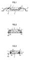
- FIG. 1 is a schematic structural view of a related art Quad Flat Package (QFP) as an IC chip.
- FIG. 2 is a schematic structural view of a related art electronic circuit board manufactured by an old type Chip On Board (COB) process wherein a bare chip 2 as an IC ship is connected to a wiring board by wire bonding.
- FIG. 3 is a schematic structural view of a related art electronic circuit board manufactured by a new type Chip On Board (COB) process wherein the bare chip is mounted as a flip chip.
- COB Chip On Board
- the lead electrodes 3 project from a side surface of the package 4 in the shape of gull wings.
- the lead electrodes 3 lead electric input or output of the bare chip 2 provided in the package 4 to a wiring board not shown in FIG. 1.
- Such mounting of the bare chip 2 is done by a Surface Mount technology (SMT).
- SMT Surface Mount technology
- a solder paste lump is printed on the electrode 101 of the wiring board 100 by a mask printing method.
- a chip such as an IC chip or chip condenser is mounted on the wiring board 100 so that an electrode pad 1 formed on a lower surface of the chip part comes in contact with the printed solder paste lump.
- solder particles in the solder paste lump are melted then made solid, so that the electrode 101 of the wiring board 100 and the electrode pad of the chip are connected by the solder 6.
- the bare chip 2 is mounted on the wiring board without providing the wire used for the wired bonding. Under this structure, it is possible to make the mounting area smaller because the wire 5 is not provided to the outside of the bare chip 2.
- a gap is formed between the lower surface of the bare chip 2 and the surface of the wiring board 100.
- Such a gap is filled with an underfill material 7.
- An inventor of the present invention determined that the educed amount of gold against the solder 6 becomes smaller by reducing the thickness of the Au surface layer of the electrode 101.
- the thickness of the Au surface layer may be approximately 2 ⁇ m, it is not possible to prevent the solder 6 from becoming fragile.
- electroless plating since the thickness of the Au surface layer may be approximately several hundreds nm, it is possible to sufficiently prevent the solder 6 from becoming fragile.
- a wiring board including: a substrate made of an insulation material and wired by a conductive material; wherein a plurality of electrodes is formed on a surface of the substrate; and a non-Au electrode not having an Au surface layer and an Au electrode having the Au surface layer are formed as the electrodes.
- an electronic circuit board including: a wiring board where a plurality of electrodes is formed on a surface of a substrate which substrate is made of an insulation material and wired by a conductive material; and a plurality of electronic parts having contact electrodes configured to connect to the electrodes formed on the surface of the substrate, the electronic parts being surface-mounted on the wiring board; wherein the wiring board includes non-Au electrodes not having Au surface layers and Au electrodes having the Au surface layers as the electrodes; at least one of the electronic parts has the Au electrode having the Au surface layer as the contact electrode; the Au surface layer has a flat contact surface having an area greater than the area of a side surface of the Au surface layer; and the contact surface is soldered to the non-Au electrode of the wiring board.
- FIG. 6 is a plan view seen from a first surface side of a Printed Wiring Board (PWB) 150.
- PWB Printed Wiring Board
- plan areas of the non-Au electrodes 151 formed in at least the flip chip mounting area R3 are less than 0.049 mm 2 and all of the Au electrodes 152 have plan areas equal to or greater than 0.049 mm 2 .
- plan areas of the non-Au electrodes 151 formed in the flip chip mounting area R3 less than 0.049 mm 2 , it can be used for mounting a small size flip chip.
- all of the Au electrodes 152 having the plan areas equal to or greater than 0.049 mm 2 oxidation of all of the electrodes formed on the second surface of the substrate 153 can be prevented by the Au surface layer 152c.
- the underfill material 502 jetted from the inclination part may come in contact with both the flip chip 301 and the module board 210.
- the underfill material 502 becomes solid based on evaporation of the solvent.
- All of or a part of the non-Au electrodes may have plan areas less than 0.049 mm 2 , and all of the Au electrodes may have plan areas equal to or greater than 0.049 mm 2 .
- the flip chip 301 is mounted on the PWB 150 so that the solder paste lumps 203 and the contact electrodes 301d are stacked.
- the present invention can be applied to a wiring board such as a printed wiring board where plural electrodes are formed on a surface of a substrate made of an insulation material for mounting an electronic part such as IC chip or a condenser, an electronic circuit board, an electronic apparatus and a manufacturing method of the electronic circuit board.
- a wiring board such as a printed wiring board where plural electrodes are formed on a surface of a substrate made of an insulation material for mounting an electronic part such as IC chip or a condenser, an electronic circuit board, an electronic apparatus and a manufacturing method of the electronic circuit board.
Landscapes
- Engineering & Computer Science (AREA)
- Manufacturing & Machinery (AREA)
- Microelectronics & Electronic Packaging (AREA)
- Electric Connection Of Electric Components To Printed Circuits (AREA)
- Wire Bonding (AREA)
- Parts Printed On Printed Circuit Boards (AREA)
- Non-Metallic Protective Coatings For Printed Circuits (AREA)
- Structures For Mounting Electric Components On Printed Circuit Boards (AREA)
Abstract
Description
- The present invention relates to a wiring board such as a printed wiring board where plural electrodes are formed on a surface of a substrate made of an insulation material for mounting an electronic part such as IC chip or a condenser, an electronic circuit board, an electronic apparatus and a manufacturing method of the electronic circuit board.
- Conventionally, electronic circuit boards, such as module boards where electronic parts are mounted on wiring boards, have been widely used for various kinds of electronic apparatuses. As the size of the electronic apparatus becomes smaller, it is required to make a mounting area on a wiring board of an IC chip small. Such a requirement of small size is discussed with reference to FIG. 1 through FIG. 3.
- Here, FIG. 1 is a schematic structural view of a related art Quad Flat Package (QFP) as an IC chip. FIG. 2 is a schematic structural view of a related art electronic circuit board manufactured by an old type Chip On Board (COB) process wherein a
bare chip 2 as an IC ship is connected to a wiring board by wire bonding. FIG. 3 is a schematic structural view of a related art electronic circuit board manufactured by a new type Chip On Board (COB) process wherein the bare chip is mounted as a flip chip. - The related art Quad Flat Package (QFP) shown in FIG. 1 includes a
bare chip 2, plural lead electrodes 3, apackage 4, and others. Plural electrode pads are formed on a surface of thebare chip 2. Thepackage 4 is made of a resin material for sealing the periphery of thebare chip 2. - The lead electrodes 3 project from a side surface of the
package 4 in the shape of gull wings. The lead electrodes 3 lead electric input or output of thebare chip 2 provided in thepackage 4 to a wiring board not shown in FIG. 1. - In the
package 4, theelectrode pad 1 formed on the surface of thebare chip 2 and end parts of the lead electrodes are connected by awire 5 made of gold. This connection is made by a well-known wire bonding method. In the QFP having the above-discussed structure, the lead electrodes 3 project in the gull wing shape outside of thepackage 4 and extend straight toward thebare chip 2 inside of thepackage 4, so that most of a mounting area on the wiring board not shown in FIG. 1 is occupied by the lead electrodes 3. - In the electronic circuit board shown in FIG. 2, the
bare chip 2 is mounted on awiring board 100, not in a package where thebare chip 2 is sealed by a resin material, but unsealed. More specifically,plural electrode pads 1 on thebare chip 2 mounted on thewiring board 100 are connected toplural electrodes 101 formed on thewiring board 100 by a wire bonding method. Since lead electrodes used in the QFP shown in FIG. 1 are not necessary by such a wire connection, it is possible to make the mounting area small. Thepackage 4 made of the resin material sealing thebare chip 2 mounted on thewiring board 100 may be provided. - In the electronic circuit board shown in FIG. 3, while the
bare chip 2 is mounted on thewiring board 100 unsealed by the resin material, the way of mounting thebare chip 2 in FIG. 3 is different from the way of mounting thebare chip 2 in FIG. 2. - More specifically, in the electronic circuit board shown in FIG. 2, the
bare chip 2 is mounted on thewiring board 100 so that the electrode pad forming surface, namely a front surface of thebare chip 2, faces vertically upward. On the other hand, in the electronic circuit board shown in FIG. 3, thebare chip 2 is mounted on thewiring board 100 so that the front surface of thebare chip 2 faces vertically downward, namely in a face down flip chip state. - Such mounting of the
bare chip 2 is done by a Surface Mount technology (SMT). In the SMT, first, a solder paste lump is printed on theelectrode 101 of thewiring board 100 by a mask printing method. Next, a chip such as an IC chip or chip condenser is mounted on thewiring board 100 so that anelectrode pad 1 formed on a lower surface of the chip part comes in contact with the printed solder paste lump. By applying a reflow process, solder particles in the solder paste lump are melted then made solid, so that theelectrode 101 of thewiring board 100 and the electrode pad of the chip are connected by thesolder 6. By such an SMT, in the electronic circuit board in FIG. 3 where thebare chip 2 is mounted as the flip chip, unlike the electronic circuit board shown in FIG. 2, thebare chip 2 is mounted on the wiring board without providing the wire used for the wired bonding. Under this structure, it is possible to make the mounting area smaller because thewire 5 is not provided to the outside of thebare chip 2. - As a result of the reflow process, a gap is formed between the lower surface of the
bare chip 2 and the surface of thewiring board 100. Such a gap is filled with anunderfill material 7. - A method for manufacturing the electronic circuit board shown in FIG. 3 is discussed in
Japanese Laid-Open Patent Application Publications No. 2001-308268 No. 2003-282630 - It is general practice for the
electrode 101 of thewiring board 100 to have a structure where an Au surface layer is provided on the surface of a metal mother material such as copper by an electrolytic gold plating process. The reason why the Au surface layer is provided is as follows. - In other words, while it is general practice for copper, aluminum, or the like to be used as the metal mother material of the
electrode 101 of thewiring board 100, these metal materials may be oxidized and therefore the surface of these metal materials may be covered with an oxide film. - Since the metal mother material covered with the oxide film repels the molten solder, it is difficult to implement good solder connections. In order to realize good solder connections, an oxide film removing process may be applied to an exposed metal mother material and then the solder connection may be immediately formed.
- However, in this method, a great number of the
wiring boards 100 so made cannot be kept. If thewiring board 100 is left in an exposed state, the metal mother material is easily oxidized so that unevenness of an electric property of theelectrodes 101 is generated due to the difference in exposure terms and a stable quality cannot be kept. - On the other hand, if the
wiring boards 100 so made are not to be kept and the manufacturing process of thewiring board 100 and the mounting process of the electronic part on thewiring board 100 after the manufacturing process are continuously implemented, manufacturing costs rise and are higher than those in a case where thewiring boards 100 so made are to be kept. Because of this, an Au surface layer formed on the surface of the metal mother material is adopted as the structure of theelectrode 101. By coating the surface of the metal mother material with Au (gold), which is a metal material that is hardly oxidized, even if a great amount of thewiring boards 100 so made are as to be kept, it is possible to prevent the oxidation of the surface of theelectrode 101 and keep a state where solder can be easily provided.
Patent Publication 1:Japanese Laid-Open Patent Application Publication No. 2001-308268
Patent Publication 2:Japanese Laid-Open Patent Application Publication No. 2003-282630 - In the manufacturing methods of the electronic circuit board discussed in
Japanese Laid-Open Patent Application Publications No. 2001-308268 No. 2003-282630 solder 6 connecting thebare chip 2 and thewiring board 100 may be fragile. More specifically, as discussed above, it is general practice for theelectrode 101 of thewiring board 100 to have a structure where an Au surface layer is provided on the surface of a metal mother material by the electrolytic gold plating process. - On the other hand, recently and continuing, as the size of the
bare chip 2 becomes smaller because of the improvements of chip manufacturing techniques, the size of theelectrode pad 1 of thebare chip 2 also becomes smaller. In addition, the diameter of the electrodes formed on the wiring board becomes reduced from greater than 250 µm to less than 250 µm. In the printing process for printing the solder paste lump on the small sizedelectrode 101, it is necessary to make the thickness of the printing mask extremely thin so that the solder paste is taken out from a minute piercing hole forming the printing pattern of the printing mask. The thickness of the solder paste lump after the printing also becomes less. Thus, in a recent technique whereby the thickness of the solder paste lump is made thin, the amount per unit area of the solder 9 provided between theelectrode 101 of theboard 100 and theelectrode pad 1 of thebare chip 2 is small. When the solder particles of the solder paste lump printed on theelectrode 101 are melted by the reflow process, gold in the Au surface layer of theelectrode 101 is educed into the molten solder. If the amount of the educed gold is too much, thesolder 6 after being solidifying becomes extremely fragile. In recent techniques wherein the amount per unit area of the solder 9 is extremely small, the ratio of the educed amount of gold against thesolder 6 is large so that thesolder 6 may be extremely fragile. - An inventor of the present invention determined that the educed amount of gold against the
solder 6 becomes smaller by reducing the thickness of the Au surface layer of theelectrode 101. In an electrolytic plating process, since the thickness of the Au surface layer may be approximately 2 µm, it is not possible to prevent thesolder 6 from becoming fragile. On other hand, in electroless plating, since the thickness of the Au surface layer may be approximately several hundreds nm, it is possible to sufficiently prevent thesolder 6 from becoming fragile. - The inventor of the present invention tried to manufacture the
electrode 101 having the Au surface layer by the electroless plating process. However, thesolder 6 could not be connected to theelectrode 101 very well. This is because a large number of minute invisible holes are formed in the extremely thin Au surface layer and the metal material under the Au surface layer is exposed through the holes so that an oxide film is formed. - Next, the inventor of the present invention manufactured a
wiring board 100 where a surface of theelectrode 101 not having the Au surface layer is covered by a film of flux made of a material different from Au so that oxidation prevention film is formed on theelectrode 101. After such awiring board 100 was left for a designated time, the bare chip (flip chip) 2 was mounted on thewiring board 100 by the SMT. As a result of this, thebare chip 2 could be connected to the wiring board 10 very well without repelling the molten solder on theelectrode 101. In addition, sufficient strength could be obtained using thesolid solder 6. Hence, by covering the surface of theelectrode 101 not having the Au surface layer with the film of flux, which flux is a non-metal material, it is possible to so make and keep a large number of thewiring boards 100. Therefore, low cost manufacturing can be achieved and sufficient strength of thesolder 6 can be obtained. - However, in such a
wiring board 100, some of theplural electrodes 101 formed on thewiring board 100 cannot work well as contact electrodes. More specifically, in recent electronic apparatuses, not all of theplural electrodes 101 on thewiring board 100 work as electrodes for solder connection but some ofelectrodes 101 work as contact electrodes. Here, the contact electrode works as an electric contact between an electric apparatus main body and an electronic device detachable from the electronic apparatus main body. For example, a home television game machine may have a structure where a ROM cassette in which game software is stored can be detached from a game machine main body. Under this structure, a contact electrode for connecting the game machine main body and the ROM cassette is necessary. Because of this, a home television game machine, having a structure where the contact electrode provided on the electronic circuit board of the ROM cassette is slid on the contact electrode at the game machine main body side as accompanying attachment or detachment of the cassette so that both contact electrodes are connected, has been widely sold. - In addition, for a portable phone having a structure where a battery unit as an electronic device is attached or detached against a phone main body, it is general practice for the phone main body and the battery unit to be connected by similar contact electrodes. Surfaces of these contact electrodes are not covered with solder so as to be exposed.
- Because of this, it is preferable that an Au surface layer be provided so that the reduction of the conductivity due to the progress of the oxidation can be prevented. In addition, in a case where the contact electrodes are slid and come in contact with each other as accompanying attachment and detachment of the electronic device, the Au surface layer works effectively. Since gold (Au) is a metal material having a relatively small coefficient of sliding friction, hanging of the contact electrodes at the time of sliding and making contact can be prevented so that a smooth attachment or detachment can be done.
- On the other hand, recently, the processing speed of
bare chip 2 has become higher due to the improvement of chip manufacturing techniques. For accompanying the high speed, it is desirable that the signal transmission speed between thebare chip 2 and other electronic parts becomes high or that noise mixture is reduced. - However, there is no discussion about a technique whereby the signal transmission speed between electronic parts can be made high and noise mixture can be reduced, in
Japanese Laid-Open Patent Application Publications No. 2001-308268 No. 2003-282630 - In the manufacturing method of the electronic circuit board discussed in
Japanese Laid-Open Patent Application Publications No. 2001-308268 No. 2003-282630 bare chip 2, the underfill process may be difficult. This is because, as shown in FIG. 4,plural electrode pads 1 are concentrated on a circumference edge part of the electrode forming surface of thebare chip 2 so that theelectrode 1 is not provided in the center of the electrode forming surface. In the underfill process of thebare chip 2, as shown by an arrow in FIG. 5, an underfill material is caused to flow from an opening formed in theplural solders 6 connecting thebare chip 2 and thewiring board 100 so that the underfill material is made to go right below the chip center part by capillary action. However, if this opening is too small, sufficient capillary action cannot be obtained and therefore the underfill process may be difficult. - Accordingly, it is a general object of the present invention to provide a novel and useful wiring board, electronic circuit board, electronic apparatus and manufacturing method of the electronic circuit board, in which one or more of the problems described above are eliminated.
- More specifically, a first object of an embodiment of the present invention is to provide a wiring board whereby fragility of solder due to a great amount of gold formed on an electrode surface of the wiring board in the solder can be avoided and a part of plural electrodes can work well as a contact electrode.
- A second object of the embodiment of the present invention is to provide wiring board manufactured at low cost by being so made as to be kept.
- A third object of the embodiment of the present invention is to provide an electronic circuit board and a manufacturing method of the electronic circuit board, whereby in the electronic circuit board signal transmission speed between electronic parts can be made high and noise mixture can be reduced.
- A fourth object of the embodiment of the present invention is to provide an electronic circuit board and a manufacturing method of the electronic circuit board, whereby an underfill process of a small size electronic part can be easily done.
- The above-mentioned object of the present invention is achieved by, for example, a wiring board, including: a substrate made of an insulation material and wired by a conductive material; wherein a plurality of electrodes is formed on a surface of the substrate; and a non-Au electrode not having an Au surface layer and an Au electrode having the Au surface layer are formed as the electrodes.
- The above-mentioned object of the present invention is achieved by, for example, an electronic circuit board, including: a wiring board where a plurality of electrodes is formed on a surface of a substrate which substrate is made of an insulation material and wired by a conductive material; and a plurality of electronic parts having contact electrodes configured to connect to the electrodes formed on the surface of the substrate, the electronic parts being surface-mounted on the wiring board; wherein the wiring board includes non-Au electrodes not having Au surface layers and Au electrodes having the Au surface layers as the electrodes; at least one of the electronic parts has the Au electrode having the Au surface layer as the contact electrode; the Au surface layer has a flat contact surface having an area greater than the area of a side surface of the Au surface layer; and the contact surface is soldered to the non-Au electrode of the wiring board.
- The above-mentioned object of the present invention is achieved by, for example, An electronic apparatus, comprising: an electronic circuit board, including a wiring board where a plurality of electrodes is formed on a surface of a substrate which substrate is made of an insulation material and wired by a conductive material; and a plurality of electronic parts having contact electrodes configured to connect to the electrodes formed on the surface of the substrate, the electronic parts being surface-mounted on the wiring board; and a housing covering the electronic circuit board; wherein a non-Au electrode not having an Au surface layer and an Au electrode having the Au surface layer are formed as the electrodes formed on the surface of the substrate of the wiring board.
- The above-mentioned object of the present invention is achieved by, for example, A manufacturing method of an electronic circuit board where a plurality of electronic parts is surface-mounted on a wiring board which wiring board includes a substrate, the method including the steps of:
- printing a paste lump made of a paste containing a conductive connection material on a plurality of electrodes formed on the substrate which substrate is made of an insulation material and wired by a conductive material; mounting the electronic parts on the wiring board via the paste lump; and connecting the electrodes of the wiring board to the corresponding contact electrodes of the electronic parts by melting the conductive connect material in the paste lump; wherein the electrodes are formed on a surface of the substrate; and a
- non-Au electrode not having an Au surface layer and an Au electrode having the Au surface layer are formed as the electrodes.
- According to the present invention, it is possible to provide a wiring board whereby fragility of solder due to a great amount of gold formed on an electrode surface of the wiring board in the solder can be avoided and a part of plural electrodes can work well as a contact electrode.
- According to the present invention, it is also possible to provide a wiring board manufactured at low cost by being so made as to be kept.
- According to the present invention, it is also possible to provide an electronic circuit board and a manufacturing method of the electronic circuit board, whereby in the electronic circuit board signal transmission speed between electronic parts can be made high and noise mixture can be reduced.
- According to the present invention, it is also possible to provide an electronic circuit board and a manufacturing method of the electronic circuit board, whereby an underfill process of a small size electronic part can be easily done.
-
- FIG. 1 is a schematic structural view of a related art Quad Flat Package (QFP) as an IC chip;
- FIG. 2 is a schematic structural view of a related art electronic circuit board manufactured by an old type Chip On Board (COB) process;
- FIG. 3 is a schematic structural view of a related art electronic circuit board manufactured by a new type Chip On Board (COB) process;
- FIG. 4 is a plan view showing an electrode forming surface of a bare chip mounted on the electronic circuit board;
- FIG. 5 is an expanded perspective view of the electronic circuit board;
- FIG. 6 is a plan view seen from a first surface side of a Printed Wiring Board (PWB) of an embodiment of the present invention;
- FIG. 7 is a plan view seen from a second surface side of the Printed Wiring Board (PWB) of the embodiment of the present invention;
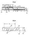
- FIG. 8 is a partially expanded cross-sectional view of the Printed Wiring Board (PWB) of the embodiment of the present invention;
- FIG. 9 is a partially expanded cross-sectional view of a plastic mask used in a manufacturing method of an electronic circuit board of an embodiment of the present invention;
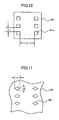
- FIG. 10 is a plan view of an electrode forming surface of a flip chip mounted on a module board manufactured by the manufacturing method of the electronic circuit board of the embodiment of the present invention;
- FIG. 11 is an expanded plan view of a half etching part of the plastic mask;
- FIG. 12 is a cross-sectional view showing a paste process implemented in a printing process of the manufacturing method of the electronic circuit board of the embodiment of the present invention;
- FIG. 13 is a cross-sectional view showing a mask removing process implemented in the printing process of the manufacturing method.of the electronic circuit board of the embodiment of the present invention;
- FIG. 14 is a cross-sectional view showing a mounting process of the manufacturing method of the electronic circuit board of the embodiment of the present invention;
- FIG. 15 is a cross-sectional view showing a reflow process of the manufacturing method of the electronic circuit board of the embodiment of the present invention;
- FIG. 16 is a cross-sectional view showing an underfill process of the manufacturing method of the electronic circuit board of the embodiment of the present invention;
- FIG. 17 is a perspective view showing the underfill process of the manufacturing method of the electronic circuit board of the embodiment of the present invention;
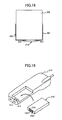
- FIG. 18 is a plan view for explaining a process for fixing the module board manufactured by the manufacturing method of the electronic circuit board of the embodiment of the present invention to a lithium battery;
- FIG. 19 is a perspective view showing a lithium battery pack where the lithium battery and the module board are provided and a main body of a portable phone;
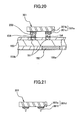
- FIG. 20 is an expanded cross-sectional view showing a flip chip mounted on the PWB by the manufacturing method of the electronic circuit board of the embodiment of the present invention;
- FIG. 21 is an expanded cross-sectional view showing a flip chip mounted on a board by a related art manufacturing method of an electronic circuit board;
- FIG. 22 is an expanded cross-sectional view showing a PWB where a related art flip chip is mounted;
- FIG. 23 is an expanded cross-sectional view showing a mounting process of the related art flip chip; and
- FIG. 24 is an expanded cross-sectional view showing the related art flip chip mounted on the PWB.
-
- 150
- PWB (Printed Wiring Board)
- 151
- Non Au-electrode
- 152
- Au electrode
- 153
- Substrate
- 203
- Paste Lump
- 301
- Flip Chip
- 301a
- Electrode pad
- 302
- SMD
- 502
- Underfil Material
- A description of the present invention and details of drawbacks of the related art are now given, with reference to FIG. 6 through FIG. 24, including embodiments of the present invention.
- More specifically, embodiments of a Printed Wiring Board (PWB) as a wiring board of the present invention, a module board as an electronic circuit board of the present invention, and a manufacturing method of the electronic circuit board are discussed.
- First, the embodiment of the Printed Wiring Board (PWB) as the wiring board of the present invention is discussed.
- FIG. 6 is a plan view seen from a first surface side of a Printed Wiring Board (PWB) 150.
- An electrode pattern of plural
non-Au electrodes 151 is formed on a first surface of thePWB 150 by a well-known technique. The first surface includes an electrode block mounting area R1, Surface Mount Device (SMD) mounting area R2, and a flip chip mounting area R3. - The electrode block mounting area R1 is where an electrode block discussed later are mounted. The
non-Au electrodes 151 of the electrode pattern in this area have rectangular shaped-configurations and big sizes whose length is approximately 10 mm. - The SMD mounting area R2 is where an electronic part such as a chip condenser different from a bare chip is surface-mounted. The
non-Au electrodes 151 of the electrode pattern in this area have small size plan areas equal to or greater than 0.049 mm2. - The flip chip mounting area R3 is where a bare chip is surface-mounted as a flip chip. The
non-Au electrodes 151 of the electrode pattern in this area have extremely small size plan areas equal to or smaller than 0.049 mm2. - FIG. 7 is a plan view seen from a second surface side of the Printed Wiring Board (PWB) 150.
- An electrode pattern of plural
non-Au electrodes 151 is formed on a second surface of thePWB 150 by a well-known technique. The second surface includes a negative contact electrode forming area R4, a positive contact electrode forming area R5, a negative test electrode forming area R6, and a positive test electrode forming area R7. - In the negative contact electrode forming area R4, a single large
size Au electrode 152 having a rectangular shaped plane configuration is formed and works as a negative contact electrode. - In the positive contact electrode forming area R5, a single large
size Au electrode 152 having a rectangular shaped plane configuration is formed and works as a positive contact electrode. - In the negative test electrode forming area R6, a single middle
size Au electrode 152 having a circular shaped plane configuration is formed and works as a negative test electrode. - In the positive test electrode forming area R7, a single middle
size Au electrode 152 having a circular shaped plane configuration is formed and works as a positive test electrode. - FIG. 8 is a partially expanded cross-sectional view of the
PWB 150 of the embodiment of the present invention. In FIG. 8, an upper surface is indicated as a first surface and a lower surface is indicated as a second surface. - The
PWB 150 includes thenon-Au electrodes 151, theAu electrodes 152, asubstrate 153 made of glass-epoxy insulation material, anoxidation prevention film 154, a resist film 155, and others. - Plural
non-Au electrodes 151 formed on the first surface of thePWB 150 have single layer structures made of only copper as a metal mother material. While illustration is omitted in FIG. 8 for convenience of explanation, the surface of thenon-Au electrode 151 is covered with theoxidation prevention film 154 formed by a flux made of a material different from gold (Au). The thickness of thenon-Au electrode 151 is approximately 35 µm. - A first resist
layer 155a is provided on a substrate area where thenon-Au electrodes 151 are not formed in the first surface of thePWB 150. The surface of thenon-Au electrodes 151 is situated at the same height as the surface of the first resistlayer 155a. The first resistlayer 155a is formed on the first surface of thesubstrate 153 in a non-Au electrode forming process by a well-known photolithography method. - A material other than flux may be used in forming the
oxidation prevention film 154. However, the material has to be different from gold (Au). This is because the solder may become fragile if gold (Au) is used as the material forming theoxidation prevention film 154. In addition, in a case where the fragility of the solder due to educed metal material other than gold (Au) may be a problem, theoxidation prevention film 154 may be made of a non-metal material. Flux is a material different from gold (Au) and a non-metal material. - As the flux, a well-known material whose main ingredient is rosin can be used. The rosin is a main ingredient forming the flux and is made of aliphatic carboxylic acid such as abietic acid. The rosin prevents the oxidation of the electrode surface so that good wetting of the molten solder against the electrode surface can be obtained. A material where another material improving an oxide removing action such as aliphatic amine halogenated hydroacid salt like diethylamine hydrochloride, or cyclohexylamine hydrobromide or aliphatic carboxylic acid like succinic acid or malonic acid is added may be used, other than rosin. In addition, instead of rosin, various kinds of non-metal organic materials or non-metal inorganic materials are used as the main ingredient of the flux. While the flux is formed by liquifying the rosin or the like in a solvent such as alcohol, the solvent evaporates so that the solid state
oxidation prevention film 154 remains after the flux is applied to the surface of thenon-Au electrode 151. When the flux is applied to the entire first surface of thePWB 150, the flux on the first resistlayer 155a is repelled so as to gather on the surface of thenon-Au electrodes 151. Thus, theoxidation prevention film 154 is formed on almost only the surface of thenon-Au electrodes 151 by applying the flux to the entire first surface of thePWB 150. - The
non-Au electrodes 151 formed in the flip chip mounting area R3 of the first surface of thesubstrate 153 have a rectangular-shaped plan area of 100 µm by 100 µm. - The Au electrodes formed on the second surface of the
PWB 150 include amother material layer 152a, anintermediate layer 152b, and anAu surface layer 152c. - The
mother material layer 152a is made of copper being a metal mother material. Theintermediate layer 152b made of nickel (Ni) is provided on themother material layer 152a. TheAu surface layer 152c made of gold (Au) is provided on theintermediate layer 152b. Theintermediate layer 152b is provided on themother material layer 152a by a well-known nickel plating process. Via theintermediate layer 152b, theAu surface layer 152c is fixed to themother material layer 152a made of copper (Cu) to which gold may not be fixed. TheAu surface layer 152c is provided on theintermediate layer 152b by a well-known electrolytic gold plating process. The thicknesses of theintermediate layer 152b and theAu surface layer 152c are several µm. - A second resist
layer 155b is provided on a substrate area where theAu electrodes 152 are not formed in the second surface of thePWB 150. The surface of theAu electrodes 152 is situated at the same height as the surface of the second resistlayer 155b. The second resistlayer 155b is formed on the second surface of thesubstrate 153 in a non-Au electrode forming process by a well-known photolithography method. - In the
PWB 150 having the above-discussed structure, thenon-Au electrode 151 not having the Au surface layer and theAu electrodes 152 having theAu surface layer 152c are formed as electrodes on thesubstrate 153 made of glass-epoxy, an insulation material. In addition, theoxidation prevention film 154 made of flux, a non-metal material, is formed on the surface of thenon-Au electrodes 151. - Under this structure, oxidation of the surface of the
non-Au electrodes 151, where the Au surface layer is not provided, is prevented by theoxidation prevention film 154 made of the flux so that the surface of thenon-Au electrodes 151 keeps, for a long period of time, a state where solder can be successfully provided. - As a result of this, it is possible to so make and keep a large number of the
PWBs 150 so that manufacturing cost of the electronic circuit board can be reduced. In addition, when a small size electronic part such as a bare chip is soldered to thenon-Au electrode 151, even if the amount of the solder provided between the electrode pad of the small size electronic part and thenon-Au electrode 151 has to be minute because the size of the electrode pad is extremely small, no gold is disposed from thenon-Au electrode 151 to the solder. Therefore, it is possible to avoid the fragility of the solder due to a large amount of educed gold of the electrode surface in the solder. In addition, since theAu electrode 152 having theAu surface layer 152c, other than thenon-Au electrodes 151, is formed, the oxidation of themother material layer 152a is prevented so that themother material layer 152a can work well as the contact electrode such as a slide type contact electrode. - Furthermore, in the
PWB 150 of the embodiment of the present invention, plural electrodes are formed on both surfaces of thesubstrate 153. All of plural electrodes formed on the first surface of the substrate are thenon-Au electrodes 151. All of plural electrodes formed on the second surface of the substrate are theAu electrodes 152. - Under this structure, it is possible to simplify the electrode forming process so that manufacturing cost can be reduced, as compared with a case where different kinds of electrodes such as the non-Au electrode and the Au electrode are formed and mixed on the same surface of the
substrate 153. - In addition, in the
PWB 150 of the embodiment of the present invention, plan areas of thenon-Au electrodes 151 formed in at least the flip chip mounting area R3 are less than 0.049 mm2 and all of theAu electrodes 152 have plan areas equal to or greater than 0.049 mm2. By making the plan areas of thenon-Au electrodes 151 formed in the flip chip mounting area R3 less than 0.049 mm2, it can be used for mounting a small size flip chip. Hence, it is possible to surface-mount a recent small size bare chip as a flip chip on the first surface of thesubstrate 153. By making all of theAu electrodes 152 having the plan areas equal to or greater than 0.049 mm2, oxidation of all of the electrodes formed on the second surface of thesubstrate 153 can be prevented by theAu surface layer 152c. - FIG. 9 is a partially expanded cross-sectional view of a plastic mask used as a printing mask when surface mounting by the STM on the
PWB 150 of the embodiment of the present invention is implemented. - The plastic printing mask is formed by a printing pattern of plural piercing
holes 202 in a plastic plate made of a material such as polyethylene terephthalate (PET) by an excimer laser process. This printing pattern corresponds to the electrode pattern formed on the first surface of thePWB 150 of the embodiment of the present invention. - An area shown by "R8" in FIG. 9 in the entire area in a surface direction of the
plastic mask 200 is ahalf etching part 203 that is more recessed than other areas. This recess is also formed by the excimer laser process. Theplastic plate 201 has a thickness of 75 µm. Cutting by the excimer laser process is done so that thehalf etching part 203 has a depth of 25 µm. - The area show by "R8" in FIG. 9 where the
half etching part 203 is formed corresponds to the flip chip mounting area R3 in the first surface of thePWB 150 shown in FIG. 6. Via plural piercing holes 202 formed in thehalf etching part 203 of theplastic mask 200, minute solder paste lumps are printed on plural flip chipnon-Au electrodes 151 formed in the flip chip mounting area R3 of thePWB 150. - As shown in FIG. 9, diameters of plural piercing
holes 202 formed in thehalf etching part 203 are extremely smaller than diameters of plural piercingholes 202 formed outside thehalf etching part 203. This is because the size of the electrode pads of the flip chip is extremely small. By reducing the length of the piercingholes 202 having the small diameter by forming thehalf etching part 203, the solder paste can be suitably taken out from theholes 202. The piercing holes 202 formed by the excimer laser process have good internal wall smoothness by cutting based on an ablation phenomenon so as to improve the ability for taking out the solder, as compared with the piercing holes formed in a metal mask. - FIG. 10 is a plan view of an electrode forming surface of a
flip chip 301. - As shown in FIG. 10, six
electrode pads 301a are formed at a periphery edge part of the electrode forming surface. More specifically, two electrode lines formed by threecontact electrode pads 301a are provided at two edge parts facing each other among four edge parts corresponding to four sides of the rectangular-shaped electrode forming surface.Electrode pads 301a are provided at end parts of the electrode lines. Length L1 between theelectrode pads 301a is equal to or greater than 500 µm. On the other hand, length L2 between the electrode pads neighboring in the electrode line is less than 500 µm. A plan area of theelectrode pad 301a is equal to or greater than 100 µm ×100 µm = 0.01 mm2. This is the smallest among the electrode pads of plural electronic parts mounted on the above-discussedPWB 150. As shown in FIG. 5, in a case where plural electrode lines are provided at the periphery edge parts, it is necessary for the distance between the electrode lines facing each other situated at a center side to be equal to or greater than 500 µm. - FIG. 11 is an expanded plan view of the area R8 of the
plastic mask 200. - It is general practice to form the piercing hole in the printing mask where the opening of the piercing hole has a circular shaped-configuration. However, in a case of the piercing hole having a minute diameter corresponding to the extremely small electrode like the
electrode pad 301a of theflip chip 301 shown in FIG. 10, if the opening has a circular shaped-configuration, it is difficult to supply the solder paste squeezed in the printing process into the piercing hole. The inventor of the present invention found that solder paste can be supplied into the piercing hole by, as shown in FIG. 11, making the openings of the minute piercing holes have a diamond shaped-configuration and making a sharp edge of the diamond shaped-configuration face in a solder squeezing direction, namely the direction shown by an arrow in FIG. 11. Hence, in the manufacturing method of the electronic circuit substrate of the embodiment of the present invention, theplastic mask 200 having a structure where the piercing hole in the area R8 (in the half etching part) is formed like this, is used. The length L3 in a longitudinal direction in the diamond shaped opening is 130 µm and the length L4 in a short direction in the diamond shaped opening is 100 µm. - FIG. 12 through FIG. 16 are views showing processes of the manufacturing method of the electronic circuit board for obtaining a module board as the electronic circuit board by mounting the electronic part on the
PWB 150 of the embodiment of the present invention. In FIG. 12 through FIG. 16, thenumerical reference 302 indicates the SMD as the electronic part and thenumerical reference 301 represents the flip chip. - In the manufacturing method of the electronic circuit board, as shown in FIG. 12 and FIG. 13, the solder paste lumps 203 are printed on the
non-Au electrodes 151 of the first surface of thePWB 150 by using the plastic mask 200 (printing process). - Next, as shown in FIG. 14, the
electronic parts PWB 150 where the solder paste printing has been done, by using a well-known chip mounter (mounting process). - As shown in FIG. 15, solder particles (not shown) in the solder paste lumps 203 are melted by increasing the temperature of the
PWB 150 in the reflow furnace, so thatelectrodes pads non-Au electrodes 151 of the first surface of the PWB 150 (connecting process). - FIG. 20 is an expanded cross-sectional view showing a
flip chip 301 mounted on thePWB 150 by the manufacturing method of the electronic circuit board of the embodiment of the present invention. Theflip chip 301 is mounted on the first surface of thePWB 150 where thenon-Au electrodes 151 are formed. Theoxidation prevention films 154 over the surfaces of thenon-Au electrodes 151 provided on the first surface of thePWB 150. - While the solder paste lumps 203 are printed on the
oxidation prevention film 154 in the printing process, theflip chip 301 is mounted on the first surface so that theelectrode pads 301a as the contact electrodes overlap the solder paste lumps 203. Theelectrode pads 301a as the contact electrodes of theflip chip 301 are formed by a flat metalmother material pad 301b made of a non-Au material such as nickel or aluminum or a Au surface layer 301c made of gold and covered with the metalmother material pad 301b. - A projection such as a gold bump (See FIG. 21) formed on the contact electrode of the flip chip used in general conventionally is not formed on the Au surface 301c. The Au surface layer has a flat configuration as shown in FIG. 20. An area of the Au surface facing upward in FIG. 21 and connecting to the substrate electrode is slightly greater than an area of a side surface in a thickness direction of the Au surface layer.
- By mounting the
flip chip 301 having the Au surface layer 301c on the first surface of thePWB 150, as shown in FIG. 20, the AU surface layer 301c comes in contact with only the surface of thesolder paste lump 203. - By applying the reflow process in this state, the amount of educed gold in the molten solder can be reduced, as compared with a case where the reflow process is applied in a state where the
gold bump 301f shown in FIG. 24 is taken into thesolder paste lump 203. As a result of this, it is possible to prevent fragility of the solder connection due to educed gold used for the contact electrode of the flip chip in the molten solder. - In a case where the Au surface layer 301c is formed in a flat shape as shown in FIG. 20, the
solder paste lump 203 is pushed and crushed when theflip chip 301 is mounted on thePWB 150 by the mounter so that a necessary gap may not be secured between the lower surface of the chip and the substrate surface. However, the inventor of the present invention found that the crushing of thesolder paste lump 203 may be avoided by making the speed of an arm where the chip is held at its head end of the mounter slow just before theflip chip 301 comes in contact with thesolder paste lump 203. - After the connection process by the reflow is applied, as shown in FIG. 16, an underfill process is applied so that the
underfill material 502 is supplied in a gap between the electrode forming surface of theflip chip 301 and the part mounting surface of thewiring board 150. - The inventor of the present invention found that, through the actual above-mentioned processes, the height of the gap after the reflow process is applied is approximately 50 through 60 µm, being less than 70 µm. The cleaning process prior to the under fill process is not implemented. The reason why the cleaning process is not necessary is as discussed above. By the above-mentioned processes, the
module board 210 as the electronic circuit board where the electronic parts are mounted on thePWB 150 is manufactured. - It is preferable to used a lead-free solder paste whose solder particles have a diameter of 10 through 30 µm. The smaller the average particle diameter of the solder paste, the better is the solder paste connection ability.
- In the underfill process, as shown in FIG. 17, the
underfill material 502 flows in a side surface whose distance between theelectrode pads 301a is equal to or greater than 500 µm among four side surfaces of theflip chip 301. - While an obliquely cut inclination part at a head end of a
nozzle 501 faces the gap between the first surface of themodule board 210 and theflip chip 301, theunderfill material 502 jetted from the inclination part may come in contact with both theflip chip 301 and themodule board 210. As a result of this, because of capillary action, it is possible to make theunderfill material 502 spread evenly throughout the depth of the gap. Theunderfill material 502 becomes solid based on evaporation of the solvent. - In the
module board 210 as the electronic circuit board, since the flip chip is surface mounted by the SMT, it is possible to drastically reduce impedance between the flip chip and the substrate electrode as compared with a case where the flip chip and the substrate electrode are connected by wire bonding. For example, while the impedance in the case of the wire bonding is 30 mΩ, the impedance in this embodiment is 15 mΩ. Because of this, it is possible to manufacture themodule board 210 strong against noise and proper for high speed processing. - In addition, the thickness of the solder connecting each of the
flip chip 301 and thenon-Au electrode 151 of thewiring board 150 is equal to or less than 70 µm. Hence, as a compared with a case where the thickness of the solder connecting each of theflip chip 301 and thenon-Au electrode 151 of thewiring board 150 is equal to or greater than 100 µm, it is possible to make signal transmission speed high and reduce mixture of the noise. In addition, it is possible to easily implement the underfill process of theflip chip 301 by flowing in theunderfill material 502 from the opening whose distance L1 between theelectrode pads 301a, namely between the solders, is equal to or greater than 500 µm. - It is also possible to make a package by sealing the periphery of the
flip chip 301 by resin. In a case whereplural flip chips 301 are mounted on thePWB 150, after the sealing resin flows in plural concave parts of a mold member corresponding to theflip chips 301, the resin in the mold contacts the first surface and is separated from the mold so that the sealing process can be applied at the same time to plural flip chips. While acrylic resin, epoxy resin, silicon resin and other can be used as the sealing resin, the epoxy resin is most preferable. - The
module board 210 manufactured by the above-discussed processes can be used as a battery protection module of a mobile phone as an electronic apparatus, for example. More specifically, themodule board 210 can be used as a module for preventing an excess current from flowing in a lithium battery at the time of charging the lithium battery pack of the mobile phone. In this case, as shown in FIG. 18, one of the twoelectrode blocks 303 mounted on the first surface is welded to apositive metal ribbon 401 extending from inside of thelithium battery 400. Furthermore, the remaining of the twoelectrode blocks 303 is welded to apositive metal ribbon 402 extending from inside of thelithium battery 400. Under this structure, theAu electrode 152 having a rectangular shaped-configuration and formed in the negative contact electrode forming area R4 in the second surface of the substrate shown in FIG. 7 is electrically connected to the negative electrode of thelithium battery 400 and works as a negative contact electrode. Furthermore, theAu electrode 152 having a rectangular shaped-configuration and formed in the negative contact electrode forming area R5 is electrically connected to the positive electrode of thelithium battery 400 and works as a positive contact electrode. In addition, theAu electrode 152 having a circular shaped-configuration and formed in the negative contact electrode forming area R6 is electrically connected to the negative electrode of thelithium battery 400 and works as a negative contact electrode. Furthermore, theAu electrode 152 having a circular shaped-configuration and formed in the negative contact electrode forming area R7 electrically connects to the positive electrode of thelithium battery 400 and works as a positive contact electrode. The negative test electrode or the positive test electrode is used for inspecting the lithium battery pack. - A
battery pack 410 having the above-discussedlithium battery 400, themodule board 210, and others is attached or detached against the phonemain body 411 of the mobile phone, as shown in FIG. 19. When thebattery pack 410 is attached or detached against the phonemain body 411 of the mobile phone, thenegative contact electrode 152Y or thepositive contact electrode 152Y are slid and moved on thenegative electrode 412 or thepositive electrode 413 of the phonemain body 411 of the mobile phone so that thebattery pack 410 is connected to thenegative electrode 412 or thepositive electrode 413. - Although the example of manufacturing the battery protection module where the flip chip works as an analog type integrated circuit by using the PWB of the.embodiment of the present invention is discussed, the present invention is not limited to this. For example, it is possible to manufacture an electric power protection circuit for an electronic apparatus such as an analog type Radio Frequency Identification (RFID) device, DC/DC converter, or game machine. It is also possible to manufacture an image processing module at an image forming apparatus, a digital type RAM module, or a CPU module. The analog type or digital type module can be used for a mother board of a personal computer, a hard disk drive (HDD), a car navigation system, a DVD drive, a DVD player, a digital camera, a copier, a printer, an IC tag, an IC card, an information processing apparatus, an image processing apparatus, a control apparatus, a communication apparatus, and others.
- Although the PWB using glass-epoxy as an insulation material is discussed as an example of the
board 153, the present invention can be applied to the wiring board using silicon (Si) or the like as the insulation material. In a case where theboard 153 is made of silicon, aluminum (Al) instead of copper can be used as the metal mother material of the electrode. In this case, the thickness of themother material layer 152a made of aluminum of theAu electrode 152 may be approximately 35 µm. Furthermore, the thickness of theintermediate layer 152b made by the nickel plating process or the thickness of theAu surface layer 152c made by the electrolytic plating process, as well as the case of themother material layer 152a made of copper, may be several µm. - According to the above-discussed embodiment of the present invention, it is possible to provide a wiring board, including:
- a substrate made of an insulation material and wired by a conductive material;
- wherein a plurality of electrodes is formed on a surface of the substrate; and
- a non-Au electrode not having an Au surface layer and an Au electrode having the Au surface layer are formed as the electrodes.
- When the small size electronic part such as the bare chip is soldered to the non-Au electrode having no Au surface layer, even if the amount of the solder provided between the electrode pad and the non-Au electrode is minute because the electrode pad of the small size electronic part is extremely small, gold is not educed from the non-Au electrode of the wiring board to the solder. Therefore, it is possible to avoid the fragility of the solder due to the large amount of educed gold of the electrode surface in the solder. In addition, since the Au electrode having the Au surface layer and the non-Au electrode having no Au surface layer, are formed, even if the Au electrode is used as the exposed contact electrode, the Au electrode works well.
- An oxidation prevention film made of a material different from Au may be formed on a surface of the non-Au electrode.
- The oxidation of the surface of the non-Au electrode without the Au surface layer is prevented by the oxidation prevention film made of non metal material such as a flux so that the surface of the non-Au electrode can be kept in a state where the solder can be adequately provided for a long time. Because of this, a large number of the wiring boards so made can be kept so that manufacturing cost of the electronic circuit board can be reduced.
- The electrodes may be formed on both surfaces of the substrate, all of the electrodes formed on a first surface of the substrate may be the non-Au electrodes, and all of the electrodes formed on a second surface of the substrate may be the Au electrodes.
- Since all of the electrodes formed on a first surface of the substrate are non-Au electrodes and all of the electrodes formed on a second surface of the substrate are Au electrodes, it is possible to simplify the electrode forming process as compared with a case where different kinds of the electrodes, namely, the non-Au electrodes and the Au electrode, are mixed on the same surface. As a result of this, it is possible to reduce the manufacturing cost.
- All of or a part of the non-Au electrodes may have plan areas less than 0.049 mm2, and all of the Au electrodes may have plan areas equal to or greater than 0.049 mm2.
- At least a part of the non-Au electrodes have plan areas less than 0.049 mm2 so that the non-Au electrodes can be used for mounting the small size flip chip. As a result of this, even if the chip is a small size bare chip, the chip can be surface mounted on one surface of a board as a flip chip. In addition, all of the Au electrodes have plan areas equal to or greater than 0.049 mm2. Oxidation of all of the electrodes formed at other surface of the board can be prevented by the Au surface layer.
- According to the above-discussed embodiment of the present invention, it is possible to provide an electronic circuit board, including:
- a wiring board where a plurality of electrodes is formed on a surface of a substrate which substrate is made of an insulation material and wired by a conductive material; and
- a plurality of electronic parts having contact electrodes configured to connect to the electrodes formed on the surface of the substrate, the electronic parts being surface-mounted on the wiring board;
- wherein a non-Au electrode not having an Au surface layer and an Au electrode having the Au surface layer are formed as the electrodes formed on the surface of the substrate of the wiring board.
- At least one of the electronic parts may have an Au electrode having an Au surface layer as the contact electrode, the Au surface layer may have a flat contact surface with an area greater than the area of a side surface of the Au surface layer, and the contact surface may be soldered to the non-Au electrode of the wiring board.
- According to the above-discussed embodiment of the present invention, it is possible to provide an electronic circuit board, including:
- a wiring board where a plurality of electrodes is formed on a surface of a substrate which substrate is made of an insulation material and wired by a conductive material; and
- a plurality of electronic parts having contact electrodes configured to connect to the electrodes formed on the surface of the substrate, the electronic parts being surface-mounted on the wiring board;
- wherein the wiring board includes non-Au electrodes not having Au surface layers and Au electrodes having the Au surface layers as the electrodes;
- at least one of the electronic parts has the Au electrode having the Au surface layer as the contact electrode;
- the Au surface layer has a flat contact surface having an area greater than the area of a side surface of the Au surface layer; and
- the contact surface is soldered to the non-Au electrode of the wiring board.
- It is possible to avoid the fragility of the solder due to the large amount of educed gold of the electrode surface of the wiring board and the contact electrode of the electronic part. That is, in the related art flip chip, for the purpose of prevention of bad connecting due to the oxidation of the connecting electrode for connecting the electrode of the wiring board, it is general practice for the gold bump to be formed on the surface of the contact electrode.
- FIG. 21 is an expanded cross-sectional view showing a flip chip mounted on a board by a related art manufacturing method of an electronic circuit board.
- Referring to FIG. 21,
plural contact electrodes 301d are formed on the surface of theflip chip 301. The contact electrode is formed by covering a surface of a flat metalmother material pad 301e made of the non-Au metal material such as nickel or aluminum, with anAu bump 301f. Thegold bump 301f projects from the surface of the flat metalmother material pad 301e by use of a wire boding device used in the above-discussed old type COB process. - FIG. 22 is an expanded cross-sectional view showing a PWB where a related art flip chip is mounted. FIG. 23 is an expanded cross-sectional view showing a mounting process of the related art flip chip. FIG. 24 is an expanded cross-sectional view showing the related art flip chip mounted on the PWB.
- In a case where such a
flip chip 301 is surface mounted, first, as shown in FIG. 22, the solder paste lumps 203 are printed on thenon-Au electrodes 151 of thePWB 150 as the wiring board. - As shown in FIG. 23, the
flip chip 301 is mounted on thePWB 150 so that the solder paste lumps 203 and thecontact electrodes 301d are stacked. - As a result of this, as shown in FIG. 24, the
gold bump 301f of thecontact electrode 301d is taken into thesolder paste lump 203. When the reflow process is implemented, a large amount of gold of thegold bump 301f taken into thesolder paste lump 203 is educed in the molten solder so that the solid solder becomes fragile. Because of this, an electronic part not having a gold projection provided on the surface of the contact electrode but having an Au flat contact surface layer whose area is larger than a side surface, is used. In such an electronic part, as shown in FIG. 21, the flat Au surface layer 301c made of gold and provided on a surface of the flat metalmother material pad 301b made of the non metal material is not taken in thesolder paste lump 203 but comes in contact with only the surface of thesolder paste lump 203. In this case, even if the reflow process is applied, gold is educed from the Au surface layer 301c into the molten solder at only the surface part of thepaste lump 203. Therefore, the amount of gold educed into the molten solder is reduced as compared with the electronic part having thegold bump 301f. As a result of this, it is possible to avoid the fragility of the solder due to the gold being educed, of the contact electrodes of the electronic part. - A distance between a part mounting surface of the wiring board and an electrode forming surface of one of the electronic parts, for which one electrode part a plan area of the contact electrode is smallest among the plan areas of the contact electrodes of the electronic parts, may be equal to or less than 70 µm.
- The electronic parts having the smallest plan areas of the contact electrodes, that is, the electronic parts such as the small size flip chips by which the signal transmission speed becomes high or noise mixture is reduced, are connected to the wiring board by a small amount of thin conductive connection material whereby the distance between the electrode forming surface and the part mounting surface of the wiring board after the reflow process is equal to or smaller than 70 µm. Since the small amount of thin conductive connection member has an electric resistance smaller than the related art, it is possible to make the signal transmission speed high and reduce the noise mixture.
- A distance between the contact electrodes in an area of a periphery edge part of the electrode forming surface of the one electronic part for which one electronic part the plan area of the contact electrode is smallest may be equal to or greater than 500 µm, and an underfill may be provided between the electrode forming surface and the part mounting surface. At least one of the electronic parts may be flip chip mounted so that an integrated circuit forming surface faces the wiring board.
- By providing the underfill material in the gap between the electrode forming surface of the small size electronic part and the part mounting surface of the wiring board, it is possible to avoid deformation toward the gap of the electronic part based on the difference of the thermal expansion rates of the electronic part and the wiring board. In addition, it is possible to prevent breakage of the conductive connection material based on the deformation. Furthermore, in a case where the distance between the electrode forming surface and the part mounting surface of the wiring board after the reflow process is equal to or smaller than 70 µm, it is possible to form an opening whose length in a substrate surface direction is equal to or greater than 500 µm in an area of the periphery edge part of the electronic part. Therefore, the underfill material can flow in from the opening so that the underfill process of the small size electronic part can be easily implemented.
- According to the above-discussed embodiment of the present invention, it is possible to provide an electronic apparatus, including:
- an electronic circuit board, including
a wiring board where a plurality of electrodes is formed on a surface of a substrate which substrate is made of an insulation material and wired by a conductive material; and
a plurality of electronic parts having contact electrodes configured to connect to the electrodes formed on the surface of the substrate, the electronic parts being surface-mounted on the wiring board; and - a housing covering the electronic circuit board;
- According to the above-discussed embodiment of the present invention, it is possible to provide an electronic apparatus, including:
- an electronic circuit board, including
a wiring board where a plurality of electrodes is formed on a surface of a substrate which substrate is made of an insulation material and wired by a conductive material; and
a plurality of electronic parts having contact electrodes configured to connect to the electrodes formed on the surface of the substrate, the electronic parts being surface-mounted on the wiring board; and - a housing covering the electronic circuit board;
- wherein a non-Au electrode not having an Au surface layer and an Au electrode having the Au surface layer are formed as the electrodes formed on the surface of the substrate of the wiring board of the electronic circuit board.
- According to the above-discussed embodiment of the present invention, it is possible to provide a manufacturing method of an electronic circuit board where a plurality of electronic parts is surface-mounted on a wiring board which wiring board includes a substrate, the method including the steps of:
- printing a paste lump made of a paste containing a conductive connection material on a plurality of electrodes formed on the substrate which substrate is made of an insulation material and wired by a conductive material;
- mounting the electronic parts on the wiring board via the paste lump; and
- connecting the electrodes of the wiring board to the corresponding contact electrodes of the electronic parts by melting the conductive connect material in the paste lump;
- wherein the electrodes are formed on a surface of the substrate; and
- a non-Au electrode not having an Au surface layer and an Au electrode having the Au surface layer are formed as the electrodes.
- The paste lump printed on the electrodes of the wiring board in the printing step may have a thickness whereby a distance between a part mounting surface of the wiring board and an electrode forming surface of one of the electronic parts, for which one electrode part a plan area of the contact electrode is smallest among the plan areas of the contact electrodes of the electronic parts, is equal to or less than 70 µm.
- By avoiding the cleaning process in an area facing the electrode forming surface in the part mounting surface, it is possible to reduce the manufacturing cost of the electronic circuit board. Although the underfill process cannot be done without the cleaning process in the related art, the cleaning process can be avoided because of the following reasons. In the related art, the amount of paste lump provided between the electrode forming surface of the electronic part and the part mounting surface of the wiring board is large and therefore a large amount of flux is supplied against the part mounting surface from the paste lump at the time of the reflow. Therefore, in the related art, at the time of the underfill process, the large amount of the flux adhered on the part mounting surface repels the underfill material so that flow-in of the underfill material is blocked. On the other hand, in the present invention, the amount of paste lumps provided between the electrode forming surface of the electronic part and the part mounting surface of the wiring board is extremely small and therefore the amount of flux supplied against the part mounting surface from the paste lump at the time of the reflow is small. Hence, in the present invention, the underfill material can flow in even if the cleaning process whereby the flux is cleaned is not implemented.
- The present invention is not limited to the above-discussed embodiments, but variations and modifications may be made without departing from the scope of the present invention.
- The present invention can be applied to a wiring board such as a printed wiring board where plural electrodes are formed on a surface of a substrate made of an insulation material for mounting an electronic part such as IC chip or a condenser, an electronic circuit board, an electronic apparatus and a manufacturing method of the electronic circuit board.
Claims (16)
- A wiring board, comprising:a substrate made of an insulation material and wired by a conductive material;wherein a plurality of electrodes is formed on a surface of the substrate; anda non-Au electrode not having an Au surface layer and an Au electrode having the Au surface layer are formed as the electrodes.
- The wiring board as claimed in claim 1,
wherein an oxidation prevention film made of a material different from Au is formed on a surface of the non-Au electrode. - The wiring board as claimed in claim 1 or 2,
wherein the electrodes are formed on both surfaces of the substrate;
all of the electrodes formed on a first surface of the substrate are the non-Au electrodes; and
all of the electrodes formed on a second surface of the substrate are the Au electrodes. - The wiring board as claimed in claim 3,
wherein all of or a part of the non-Au electrodes have plan areas less than 0.049 mm2; and
all of the Au electrodes have plan areas equal to or greater than 0.049 mm2. - An electronic circuit board, comprising:a wiring board where a plurality of electrodes is formed on a surface of a substrate which substrate is made of an insulation material and wired by a conductive material; anda plurality of electronic parts having contact electrodes configured to connect to the electrodes formed on the surface of the substrate, the electronic parts being surface-mounted on the wiring board;wherein a non-Au electrode not having an Au surface layer and an Au electrode having the Au surface layer are formed as the electrodes formed on the surface of the substrate of the wiring board.
- The electronic circuit board as claimed in claim 5,
wherein at least one of the electronic parts has an Au electrode having an Au surface layer as the contact electrode;
the Au surface layer has a flat contact surface with an area greater than the area of a side surface of the Au surface layer; and
the contact surface is soldered to the non-Au electrode of the wiring board. - An electronic circuit board, comprising:a wiring board where a plurality of electrodes is formed on a surface of a substrate which substrate is made of an insulation material and wired by a conductive material; anda plurality of electronic parts having contact electrodes configured to connect to the electrodes formed on the surface of the substrate, the electronic parts being surface-mounted on the wiring board;wherein the wiring board includes non-Au electrodes not having Au surface layers and Au electrodes having the Au surface layers as the electrodes;at least one of the electronic parts has the Au electrode having the Au surface layer as the contact electrode;the Au surface layer has a flat contact surface having an area greater than the area of a side surface of the Au surface layer; andthe contact surface is soldered to the non-Au electrode of the wiring board.
- The electronic circuit board as claimed in claim 5, 6, or 7,
wherein a distance between a part mounting surface of the wiring board and an electrode forming surface of one of the electronic parts, for which one electrode part a plan area of the contact electrode is smallest among the plan areas of the contact electrodes of the electronic parts, is equal to or less than 70 µm. - The electronic circuit board as claimed in claim 8,
wherein a distance between the contact electrodes in an area of a periphery edge part of the electrode forming surface of the one electronic part for which one electronic part the plan area of the contact electrode is smallest is equal to or greater than 500 µm; and
an underfill is provided between the electrode forming surface and the part mounting surface. - The electronic circuit board as claimed in one of claims 5 through 9,
wherein at least one of the electronic parts is flip chip mounted so that an integrated circuit forming surface faces the wiring board. - An electronic apparatus, comprising:an electronic circuit board, including
a wiring board where a plurality of electrodes is formed on a surface of a substrate which substrate is made of an insulation material and wired by a conductive material; and
a plurality of electronic parts having contact electrodes configured to connect to the electrodes formed on the surface of the substrate, the electronic parts being surface-mounted on the wiring board; anda housing covering the electronic circuit board;wherein a non-Au electrode not having an Au surface layer and an Au electrode having the Au surface layer are formed as the electrodes formed on the surface of the substrate of the wiring board. - An electronic apparatus, comprising:an electronic circuit board, including
a wiring board where a plurality of electrodes is formed on a surface of a substrate which substrate is made of an insulation material and wired by a conductive material; and
a plurality of electronic parts having contact electrodes configured to connect to the electrodes formed on the surface of the substrate, the electronic parts being surface-mounted on the wiring board; anda housing covering the electronic circuit board;wherein a non-Au electrode not having an Au surface layer and an Au electrode having the Au surface layer are formed as the electrodes formed on the surface of the substrate of the wiring board of the electronic circuit board. - A manufacturing method of an electronic circuit board where a plurality of electronic parts is surface-mounted on a wiring board which wiring board includes a substrate, the method comprising the steps of:printing a paste lump made of a paste containing a conductive connection material on a plurality of electrodes formed on the substrate which substrate is made of an insulation material and wired by a conductive material;mounting the electronic parts on the wiring board via the paste lump; andconnecting the electrodes of the wiring board to the corresponding contact electrodes of the electronic parts by melting the conductive connect material in the paste lump;wherein the electrodes are formed on a surface of the substrate; and
a non-Au electrode not having an Au surface layer and an Au electrode having the Au surface layer are formed as the electrodes. - The manufacturing method of an electronic circuit board as claimed in claim 13,
wherein the paste lump printed on the electrodes of the wiring board in the printing step has a thickness whereby a distance between a part mounting surface of the wiring board and an electrode forming surface of one of the electronic parts, for which one electrode part a plan area of the contact electrode is smallest among the plan areas of the contact electrodes of the electronic parts, is equal to or less than 70 µm. - The manufacturing method of the electronic circuit board as claimed in claim 14,
wherein a distance between the contact electrodes in an area of a periphery edge part of the electrode forming surface of the one electronic part for which one electronic part the plan area of the contact electrode is smallest is equal to or greater than 500 µm; and
an underfill step is implemented after the connecting step so that an underfill material flows from a space between the area of the part of the periphery edge part of the electrode forming surface and the part mounting surface to a part under the electrode forming surface. - The manufacturing method of an electronic circuit board as claimed in claim 15,
wherein the underfill step is implemented without cleaning an area of the part mounting surface facing the electrode forming surface.
Applications Claiming Priority (4)
| Application Number | Priority Date | Filing Date | Title |
|---|---|---|---|
| JP2004235448 | 2004-08-12 | ||
| JP2004235438 | 2004-08-12 | ||
| JP2005215800A JP2006080493A (en) | 2004-08-12 | 2005-07-26 | Electrode substrate |
| PCT/JP2005/014748 WO2006016650A1 (en) | 2004-08-12 | 2005-08-11 | Electrode substrate |
Publications (2)
| Publication Number | Publication Date |
|---|---|
| EP1784065A1 true EP1784065A1 (en) | 2007-05-09 |
| EP1784065A4 EP1784065A4 (en) | 2009-07-22 |
Family
ID=35839410
Family Applications (1)
| Application Number | Title | Priority Date | Filing Date |
|---|---|---|---|
| EP05770814A Ceased EP1784065A4 (en) | 2004-08-12 | 2005-08-11 | ELECTRODE SUBSTRATE |
Country Status (5)
| Country | Link |
|---|---|
| US (1) | US7732935B2 (en) |
| EP (1) | EP1784065A4 (en) |
| JP (1) | JP2006080493A (en) |
| CN (1) | CN101023717B (en) |
| WO (1) | WO2006016650A1 (en) |
Families Citing this family (8)
| Publication number | Priority date | Publication date | Assignee | Title |
|---|---|---|---|---|
| KR100874588B1 (en) * | 2007-09-05 | 2008-12-16 | 성균관대학교산학협력단 | Flip chip capable of evaluating electrical characteristics and manufacturing method thereof |
| USRE48422E1 (en) * | 2007-09-05 | 2021-02-02 | Research & Business Foundation Sungkyunkwan Univ. | Method of making flip chip |
| CN102646606B (en) * | 2011-02-16 | 2014-12-24 | 中电智能卡有限责任公司 | Packaging method of integrated circuit (IC) card module |
| JP6045436B2 (en) * | 2013-05-02 | 2016-12-14 | ルネサスエレクトロニクス株式会社 | Electronic equipment |
| US9425157B2 (en) | 2014-02-26 | 2016-08-23 | Taiwan Semiconductor Manufacturing Company Limited | Substrate and package structure |
| CN104308314A (en) * | 2014-10-11 | 2015-01-28 | 昆山圆裕电子科技有限公司 | Reflow welding process of DIP through-hole part |
| JP6889399B2 (en) * | 2017-08-08 | 2021-06-18 | 大日本印刷株式会社 | Through silicon via substrate |
| CN113921404A (en) * | 2021-09-24 | 2022-01-11 | 青岛歌尔微电子研究院有限公司 | Packaging method of system-level packaging structure |
Family Cites Families (30)
| Publication number | Priority date | Publication date | Assignee | Title |
|---|---|---|---|---|
| US3394527A (en) * | 1967-07-24 | 1968-07-30 | American Cyanamid Co | Reinforcing anisotropic non-homogeneous engineering structures |
| JPS58192351A (en) | 1982-05-06 | 1983-11-09 | Sharp Corp | Manufacture of semiconductor device |
| JPH02296336A (en) | 1989-05-10 | 1990-12-06 | Seiko Epson Corp | Manufacture of semiconductor circuit bump |
| JPH05167236A (en) * | 1991-12-19 | 1993-07-02 | Sumitomo Bakelite Co Ltd | Soldering to circuit, etc. |
| JPH07193166A (en) * | 1993-11-19 | 1995-07-28 | Citizen Watch Co Ltd | Semiconductor device with solder bumps and method of manufacturing the same |
| FI940953A7 (en) * | 1994-02-28 | 1995-08-29 | Optatech Oy | Polymer films and method for their preparation |
| US6524644B1 (en) * | 1999-08-26 | 2003-02-25 | Enthone Inc. | Process for selective deposition of OSP coating on copper, excluding deposition on gold |
| US6534192B1 (en) * | 1999-09-24 | 2003-03-18 | Lucent Technologies Inc. | Multi-purpose finish for printed wiring boards and method of manufacture of such boards |
| JP3952434B2 (en) | 2000-03-29 | 2007-08-01 | ローム株式会社 | Battery pack and manufacturing method thereof |
| DE10018025A1 (en) * | 2000-04-04 | 2001-10-18 | Atotech Deutschland Gmbh | Production of solderable surface on circuit carriers in circuit board manufacture comprises preparing a dielectric substrate having copper structures, producing solderable surfaces, and forming functional surfaces in functional regions |
| JP3855592B2 (en) | 2000-04-19 | 2006-12-13 | 松下電器産業株式会社 | Manufacturing method of small module |
| JP3477656B2 (en) * | 2000-06-21 | 2003-12-10 | 三洋ジ−エスソフトエナジー株式会社 | Battery external terminal and battery pack using it |
| TW511257B (en) * | 2000-12-11 | 2002-11-21 | Chino Excel Technology Corp | Flip-chip mounting method for decreasing conducting resistance in power transistor of charging battery protection circuit |
| US6494361B1 (en) * | 2001-01-26 | 2002-12-17 | Amkor Technology, Inc. | Semiconductor module package substrate fabrication method |
| US6515744B2 (en) * | 2001-02-08 | 2003-02-04 | Therma-Wave, Inc. | Small spot ellipsometer |
| JP3792129B2 (en) * | 2001-03-01 | 2006-07-05 | 新光電気工業株式会社 | Capacitor, capacitor built-in circuit board, and manufacturing method thereof |
| US6744135B2 (en) * | 2001-05-22 | 2004-06-01 | Hitachi, Ltd. | Electronic apparatus |
| JP2002368038A (en) * | 2001-06-07 | 2002-12-20 | Fuji Electric Co Ltd | Flip chip mounting method |
| JP3866591B2 (en) | 2001-10-29 | 2007-01-10 | 富士通株式会社 | Method for forming interelectrode connection structure and interelectrode connection structure |
| US7130198B2 (en) * | 2001-12-06 | 2006-10-31 | Rohm Co., Ltd. | Resin-packaged protection circuit module for rechargeable batteries and method of making the same |
| JP3872995B2 (en) | 2002-03-20 | 2007-01-24 | Tdk株式会社 | Bare chip mounting method |
| JP2003318308A (en) * | 2002-04-18 | 2003-11-07 | Nippon Mektron Ltd | Circuit pattern for connecting flip-chip ic of flexible circuit substrate |
| JP2004165637A (en) * | 2002-10-21 | 2004-06-10 | Matsushita Electric Ind Co Ltd | Semiconductor device |
| JP2004171964A (en) * | 2002-11-20 | 2004-06-17 | Sony Corp | Circuit board, battery connection method, and power supply device |
| CN100405881C (en) * | 2003-03-18 | 2008-07-23 | 日本特殊陶业株式会社 | Wiring board |
| US7141874B2 (en) * | 2003-05-14 | 2006-11-28 | Matsushita Electric Industrial Co., Ltd. | Electronic component packaging structure and method for producing the same |
| JP4033811B2 (en) | 2003-06-19 | 2008-01-16 | 株式会社リコー | Flip chip mounting body |
| US7186645B2 (en) * | 2003-10-13 | 2007-03-06 | Intel Corporation | Selective plating of package terminals |
| WO2005069486A1 (en) * | 2004-01-19 | 2005-07-28 | Murata Manufacturing Co., Ltd. | Acoustic boundary wave device |
| JP4736451B2 (en) * | 2005-02-03 | 2011-07-27 | パナソニック株式会社 | MULTILAYER WIRING BOARD, MANUFACTURING METHOD THEREOF, AND SEMICONDUCTOR PACKAGE AND ELECTRONIC DEVICE USING MULTILAYER WIRING BOARD |
-
2005
- 2005-07-26 JP JP2005215800A patent/JP2006080493A/en active Pending
- 2005-08-11 WO PCT/JP2005/014748 patent/WO2006016650A1/en not_active Ceased
- 2005-08-11 EP EP05770814A patent/EP1784065A4/en not_active Ceased
- 2005-08-11 CN CN2005800266184A patent/CN101023717B/en not_active Expired - Fee Related
-
2006
- 2006-04-20 US US11/408,123 patent/US7732935B2/en not_active Expired - Fee Related
Also Published As
| Publication number | Publication date |
|---|---|
| CN101023717A (en) | 2007-08-22 |
| US7732935B2 (en) | 2010-06-08 |
| EP1784065A4 (en) | 2009-07-22 |
| JP2006080493A (en) | 2006-03-23 |
| WO2006016650A1 (en) | 2006-02-16 |
| CN101023717B (en) | 2010-05-05 |
| US20060214297A1 (en) | 2006-09-28 |
Similar Documents
| Publication | Publication Date | Title |
|---|---|---|
| JP3565047B2 (en) | Solder bump forming method and solder bump mounting method | |
| KR20080017431A (en) | Manufacturing method of printed wiring board and printed wiring board | |
| EP0889512A2 (en) | Method for controlling solder bump shape and stand-off height | |
| JP2002208668A (en) | Semiconductor device and method of manufacturing the same | |
| US7732935B2 (en) | Wiring board, electronic circuit board, electronic apparatus and manufacturing method of electronic circuit board | |
| JP2018137276A (en) | Printed circuit board and manufacturing method thereof, and electronic device | |
| KR100432325B1 (en) | Electrode forming method and bump electrode formable base used therefor | |
| US6402012B1 (en) | Method for forming solder bumps using a solder jetting device | |
| JP2000040713A (en) | Semiconductor package manufacturing method | |
| JP2004200539A (en) | Component connection terminals and electronic equipment | |
| JP4159631B2 (en) | Manufacturing method of semiconductor package | |
| JP2017130697A (en) | Thick copper wiring board | |
| JP2000151086A (en) | Printed circuit unit and method of manufacturing the same | |
| JPH11345826A (en) | Semiconductor device, method of manufacturing semiconductor device, and method of mounting semiconductor device | |
| JP3582286B2 (en) | Manufacturing method of wiring board | |
| KR100746365B1 (en) | Method for manufacturing a substrate for flip chip mounting | |
| CN1450612A (en) | Method for forming convex point on back side of single side flexible sustrate | |
| JP3493999B2 (en) | Solder bump forming method and solder bump mounting method | |
| JP2751897B2 (en) | Ball grid array mounting structure and mounting method | |
| JP2526796B2 (en) | Tape carrier package | |
| JPH11150151A (en) | Integrated circuit chip mounting structure and method | |
| JPH02165633A (en) | Manufacture of semiconductor device | |
| JP2006093178A (en) | Method for manufacturing electronic equipment | |
| JPH11307215A (en) | Method for surface mounting electronic component having terminal to be soldered and surface mounting structure therefor | |
| US20070148950A1 (en) | Object and bonding method thereof |
Legal Events
| Date | Code | Title | Description |
|---|---|---|---|
| PUAI | Public reference made under article 153(3) epc to a published international application that has entered the european phase |
Free format text: ORIGINAL CODE: 0009012 |
|
| 17P | Request for examination filed |
Effective date: 20070117 |
|
| AK | Designated contracting states |
Kind code of ref document: A1 Designated state(s): DE FR GB |
|
| DAX | Request for extension of the european patent (deleted) | ||
| RBV | Designated contracting states (corrected) |
Designated state(s): DE FR GB |
|
| A4 | Supplementary search report drawn up and despatched |
Effective date: 20090618 |
|
| 17Q | First examination report despatched |
Effective date: 20130409 |
|
| REG | Reference to a national code |
Ref country code: DE Ref legal event code: R003 |
|
| STAA | Information on the status of an ep patent application or granted ep patent |
Free format text: STATUS: THE APPLICATION HAS BEEN REFUSED |
|
| 18R | Application refused |
Effective date: 20171008 |