EP1781984B1 - Led lighting system with reflective board - Google Patents
Led lighting system with reflective board Download PDFInfo
- Publication number
- EP1781984B1 EP1781984B1 EP05771031.1A EP05771031A EP1781984B1 EP 1781984 B1 EP1781984 B1 EP 1781984B1 EP 05771031 A EP05771031 A EP 05771031A EP 1781984 B1 EP1781984 B1 EP 1781984B1
- Authority
- EP
- European Patent Office
- Prior art keywords
- light emitting
- nanometers
- solder mask
- light
- electrically insulating
- Prior art date
- Legal status (The legal status is an assumption and is not a legal conclusion. Google has not performed a legal analysis and makes no representation as to the accuracy of the status listed.)
- Expired - Lifetime
Links
Images



Classifications
-
- H—ELECTRICITY
- H05—ELECTRIC TECHNIQUES NOT OTHERWISE PROVIDED FOR
- H05K—PRINTED CIRCUITS; CASINGS OR CONSTRUCTIONAL DETAILS OF ELECTRIC APPARATUS; MANUFACTURE OF ASSEMBLAGES OF ELECTRICAL COMPONENTS
- H05K1/00—Printed circuits
- H05K1/18—Printed circuits structurally associated with non-printed electric components
- H05K1/181—Printed circuits structurally associated with non-printed electric components associated with surface mounted components
-
- F—MECHANICAL ENGINEERING; LIGHTING; HEATING; WEAPONS; BLASTING
- F21—LIGHTING
- F21K—NON-ELECTRIC LIGHT SOURCES USING LUMINESCENCE; LIGHT SOURCES USING ELECTROCHEMILUMINESCENCE; LIGHT SOURCES USING CHARGES OF COMBUSTIBLE MATERIAL; LIGHT SOURCES USING SEMICONDUCTOR DEVICES AS LIGHT-GENERATING ELEMENTS; LIGHT SOURCES NOT OTHERWISE PROVIDED FOR
- F21K9/00—Light sources using semiconductor devices as light-generating elements, e.g. using light-emitting diodes [LED] or lasers
-
- H—ELECTRICITY
- H01—ELECTRIC ELEMENTS
- H01S—DEVICES USING THE PROCESS OF LIGHT AMPLIFICATION BY STIMULATED EMISSION OF RADIATION [LASER] TO AMPLIFY OR GENERATE LIGHT; DEVICES USING STIMULATED EMISSION OF ELECTROMAGNETIC RADIATION IN WAVE RANGES OTHER THAN OPTICAL
- H01S5/00—Semiconductor lasers
- H01S5/005—Optical components external to the laser cavity, specially adapted therefor, e.g. for homogenisation or merging of the beams or for manipulating laser pulses, e.g. pulse shaping
- H01S5/0087—Optical components external to the laser cavity, specially adapted therefor, e.g. for homogenisation or merging of the beams or for manipulating laser pulses, e.g. pulse shaping for illuminating phosphorescent or fluorescent materials, e.g. using optical arrangements specifically adapted for guiding or shaping laser beams illuminating these materials
-
- H—ELECTRICITY
- H01—ELECTRIC ELEMENTS
- H01S—DEVICES USING THE PROCESS OF LIGHT AMPLIFICATION BY STIMULATED EMISSION OF RADIATION [LASER] TO AMPLIFY OR GENERATE LIGHT; DEVICES USING STIMULATED EMISSION OF ELECTROMAGNETIC RADIATION IN WAVE RANGES OTHER THAN OPTICAL
- H01S5/00—Semiconductor lasers
- H01S5/02—Structural details or components not essential to laser action
- H01S5/022—Mountings; Housings
- H01S5/0225—Out-coupling of light
- H01S5/02257—Out-coupling of light using windows, e.g. specially adapted for back-reflecting light to a detector inside the housing
-
- H—ELECTRICITY
- H05—ELECTRIC TECHNIQUES NOT OTHERWISE PROVIDED FOR
- H05K—PRINTED CIRCUITS; CASINGS OR CONSTRUCTIONAL DETAILS OF ELECTRIC APPARATUS; MANUFACTURE OF ASSEMBLAGES OF ELECTRICAL COMPONENTS
- H05K1/00—Printed circuits
- H05K1/02—Details
- H05K1/0274—Optical details, e.g. printed circuits comprising integral optical means
-
- H—ELECTRICITY
- H01—ELECTRIC ELEMENTS
- H01S—DEVICES USING THE PROCESS OF LIGHT AMPLIFICATION BY STIMULATED EMISSION OF RADIATION [LASER] TO AMPLIFY OR GENERATE LIGHT; DEVICES USING STIMULATED EMISSION OF ELECTROMAGNETIC RADIATION IN WAVE RANGES OTHER THAN OPTICAL
- H01S5/00—Semiconductor lasers
- H01S5/02—Structural details or components not essential to laser action
- H01S5/022—Mountings; Housings
- H01S5/02208—Mountings; Housings characterised by the shape of the housings
- H01S5/02216—Butterfly-type, i.e. with electrode pins extending horizontally from the housings
-
- H—ELECTRICITY
- H01—ELECTRIC ELEMENTS
- H01S—DEVICES USING THE PROCESS OF LIGHT AMPLIFICATION BY STIMULATED EMISSION OF RADIATION [LASER] TO AMPLIFY OR GENERATE LIGHT; DEVICES USING STIMULATED EMISSION OF ELECTROMAGNETIC RADIATION IN WAVE RANGES OTHER THAN OPTICAL
- H01S5/00—Semiconductor lasers
- H01S5/02—Structural details or components not essential to laser action
- H01S5/022—Mountings; Housings
- H01S5/0225—Out-coupling of light
- H01S5/02255—Out-coupling of light using beam deflecting elements
-
- H—ELECTRICITY
- H01—ELECTRIC ELEMENTS
- H01S—DEVICES USING THE PROCESS OF LIGHT AMPLIFICATION BY STIMULATED EMISSION OF RADIATION [LASER] TO AMPLIFY OR GENERATE LIGHT; DEVICES USING STIMULATED EMISSION OF ELECTROMAGNETIC RADIATION IN WAVE RANGES OTHER THAN OPTICAL
- H01S5/00—Semiconductor lasers
- H01S5/40—Arrangement of two or more semiconductor lasers, not provided for in groups H01S5/02 - H01S5/30
- H01S5/4025—Array arrangements, e.g. constituted by discrete laser diodes or laser bar
-
- H—ELECTRICITY
- H05—ELECTRIC TECHNIQUES NOT OTHERWISE PROVIDED FOR
- H05K—PRINTED CIRCUITS; CASINGS OR CONSTRUCTIONAL DETAILS OF ELECTRIC APPARATUS; MANUFACTURE OF ASSEMBLAGES OF ELECTRICAL COMPONENTS
- H05K2201/00—Indexing scheme relating to printed circuits covered by H05K1/00
- H05K2201/01—Dielectrics
- H05K2201/0183—Dielectric layers
- H05K2201/0195—Dielectric or adhesive layers comprising a plurality of layers, e.g. in a multilayer structure
-
- H—ELECTRICITY
- H05—ELECTRIC TECHNIQUES NOT OTHERWISE PROVIDED FOR
- H05K—PRINTED CIRCUITS; CASINGS OR CONSTRUCTIONAL DETAILS OF ELECTRIC APPARATUS; MANUFACTURE OF ASSEMBLAGES OF ELECTRICAL COMPONENTS
- H05K2201/00—Indexing scheme relating to printed circuits covered by H05K1/00
- H05K2201/02—Fillers; Particles; Fibers; Reinforcement materials
- H05K2201/0203—Fillers and particles
- H05K2201/0206—Materials
- H05K2201/0209—Inorganic, non-metallic particles
-
- H—ELECTRICITY
- H05—ELECTRIC TECHNIQUES NOT OTHERWISE PROVIDED FOR
- H05K—PRINTED CIRCUITS; CASINGS OR CONSTRUCTIONAL DETAILS OF ELECTRIC APPARATUS; MANUFACTURE OF ASSEMBLAGES OF ELECTRICAL COMPONENTS
- H05K2201/00—Indexing scheme relating to printed circuits covered by H05K1/00
- H05K2201/20—Details of printed circuits not provided for in H05K2201/01 - H05K2201/10
- H05K2201/2054—Light-reflecting surface, e.g. conductors, substrates, coatings, dielectrics
-
- H—ELECTRICITY
- H10—SEMICONDUCTOR DEVICES; ELECTRIC SOLID-STATE DEVICES NOT OTHERWISE PROVIDED FOR
- H10W—GENERIC PACKAGES, INTERCONNECTIONS, CONNECTORS OR OTHER CONSTRUCTIONAL DETAILS OF DEVICES COVERED BY CLASS H10
- H10W90/00—Package configurations
-
- Y—GENERAL TAGGING OF NEW TECHNOLOGICAL DEVELOPMENTS; GENERAL TAGGING OF CROSS-SECTIONAL TECHNOLOGIES SPANNING OVER SEVERAL SECTIONS OF THE IPC; TECHNICAL SUBJECTS COVERED BY FORMER USPC CROSS-REFERENCE ART COLLECTIONS [XRACs] AND DIGESTS
- Y02—TECHNOLOGIES OR APPLICATIONS FOR MITIGATION OR ADAPTATION AGAINST CLIMATE CHANGE
- Y02P—CLIMATE CHANGE MITIGATION TECHNOLOGIES IN THE PRODUCTION OR PROCESSING OF GOODS
- Y02P70/00—Climate change mitigation technologies in the production process for final industrial or consumer products
- Y02P70/50—Manufacturing or production processes characterised by the final manufactured product
-
- Y—GENERAL TAGGING OF NEW TECHNOLOGICAL DEVELOPMENTS; GENERAL TAGGING OF CROSS-SECTIONAL TECHNOLOGIES SPANNING OVER SEVERAL SECTIONS OF THE IPC; TECHNICAL SUBJECTS COVERED BY FORMER USPC CROSS-REFERENCE ART COLLECTIONS [XRACs] AND DIGESTS
- Y10—TECHNICAL SUBJECTS COVERED BY FORMER USPC
- Y10S—TECHNICAL SUBJECTS COVERED BY FORMER USPC CROSS-REFERENCE ART COLLECTIONS [XRACs] AND DIGESTS
- Y10S362/00—Illumination
- Y10S362/80—Light emitting diode
Definitions
- the present invention relates to the lighting arts. It especially relates to high intensity light emitting diode packages, components, apparatuses, and so forth, and will be described with particular reference thereto. However, the invention will also find application in conjunction with other solid state light emitters such as vertical cavity surface emitting lasers.
- High brightness light emitting packages typically employ a plurality of light emitting diode chips, surface emitting laser chips, organic light emitter chips, or the like. To mechanically support the chips and to electrically interconnect the chips, in some light emitting packages the light emitting chips are disposed on a printed circuit board.
- the printed circuit board can also support and electrically incorporate discrete electronic components, application-specific integrated circuits (ASICs), programmable microprocessors, or the like, for providing input power conditioning, light output control, electrostatic discharge protection, or other functions.
- ASICs application-specific integrated circuits
- microprocessors programmable microprocessors
- the printed circuit board can contribute to optical losses by partially absorbing light that impinges upon the printed circuit board.
- Printed circuit boards typically include a topmost epoxy solder mask layer having lithographically defined openings through which the light emitting chips or other electronic components electrically contact bonding pads of the printed circuitry.
- the solder mask layer is not optimized for its optical properties, and is thus not very reflective.
- white solder masks For high brightness light emitting packages, printed circuit boards having a commercially available white solder mask are sometimes used. These white solder masks contain white talc or another white material that reflects visible light. White solder masks provide a substantial improvement in reflectance of visible light over conventional blue or green solder masks.
- US 6,161,910 discloses an LED reading light assembly and has an optical assembly, a power circuit board, a housing, and a control system.
- the optical assembly includes a holographic lens and an LED assembly comprising an LED circuit board and a plurality of LED's disposed on the outward facing side of the LED circuit board.
- the power circuit board provides a constant source of electric current to power the LED's.
- the assembly includes a white solder mask.
- US 2003/193055 discloses a lighting device having a light emitting diode (LED).
- the device includes a metal substrate having a surface.
- a dielectric coating layer is superimposed on the surface of the metal substrate.
- a light emitting diode (LED) is supported on the dielectric coating layer.
- the metal substrate serves as a heat sink for the heat emitted by LED during operation.
- WO 2004047498 discloses a lighting body or a source of light comprising a lighting part with a number of light-emitting diodes (LEDs), and a power part with a power converter for converting an incoming AC or DC current to a direct current for supply of the LEDs.
- LEDs light-emitting diodes
- JP 7-288341 discloses a printed circuit board on whose surface a conductor layer is formed, at least, blue, green and red LED chips are mounted, and the whole of the three LED chips is molded, and thereby, one picture element of an LED display is formed.
- the blue LED chip comprises a gallium nitride based compound semiconductor LED chip wherein on a sapphire substrate gallium nitride based compound semiconductors are laminated. Further, the sapphire substrate of the gallium nitride based compound semiconductor chip is bonded to the printed circuit board via a transparent or white insulation bonding agent.
- US 2002177072 discloses a photoimagable cationically polymerizable epoxy based solder mask that contains a non-brominated epoxy resin system and from about 0.1 to about 15 parts, by weight per 100 parts of resin system, of a cationic photoinitiator. Since the photosensitive cationically polymerizable epoxy based solder mask does not contain bromine, it is particularly advantageous halogens in waste processing chemicals or in incinerated scrap circuit boards are regulated by environmental concerns.
- white solder masks have certain disadvantages for some high brightness light emitting packages.
- the white solder mask appears to be highly reflective, the inventors have measured the reflectance of such boards and have found that the reflectance is only about 80% or less in the visible spectral region. If 50% of the visible light produced by the light emitting package impinges on the printed circuit board, this reflectance corresponds to optical losses of around 10% or higher due to absorption in the printed circuit board.
- the reflectance of the white solder masks decreases in the blue, violet, and ultraviolet spectral regions.
- the inventors have found the white solder board reflectance decreases below 60% for wavelengths less than about 410 nm.
- wide-bandgap light emitting chips emitting blue, violet, or ultraviolet light emission are coupled with a phosphor that converts the light emission into white or another selected visible light
- a substantial amount of blue, violet, or ultraviolet light typically reflects from the phosphor toward the printed circuit board.
- the relatively low reflectance of white solder masks for blue, violet, or ultraviolet wavelength light degrades the light output efficiency of these packages.
- the present invention contemplates improved apparatuses and methods that overcomes the above-mentioned limitations and others.
- a light emitting apparatus is disclosed.
- One or more light emitting chips are disposed on a printed circuit board and emit light predominantly in a wavelength range between about 400 nanometers and about 470 nanometers.
- the printed circuit board includes: (i) an electrically insulating board; (ii) electrically conductive printed circuitry; and (iii) an electrically insulating solder mask having vias through which the one or more light emitting chips electrically contact the printed circuitry.
- the solder mask has a reflectance of greater than 60% at least between about 400 nanometers and about 470 nanometers.
- a method for fabricating a light emitting apparatus.
- An electrically insulating board is provided with electrically conductive printed circuitry disposed thereon.
- An electrically insulating solder mask is disposed on the electrically insulating board.
- the solder mask has vias accessing the printed circuitry, and has a reflectance of greater than 60% at least between about 400 nanometers and about 470 nanometers.
- One or more light emitting chips are disposed on the insulating solder mask. The one or more light emitting chips electrically contact the printed circuitry through the vias in the solder mask, and emit light predominantly in a wavelength range between about 400 nanometers and about 470 nanometers.
- a light emitting apparatus is disclosed.
- One or more light emitting chips are disposed on a printed circuit board and emit light predominantly in a wavelength range between about 400 nanometers and about 470 nanometers.
- the printed circuit board includes: (i) an electrically insulating board; (ii) electrically conductive printed circuitry; and (iii) an electrically insulating solder mask having vias through which the one or more light emitting chips electrically contact the printed circuitry.
- the solder mask has a reflectance of greater than 60% at least between about 400 nanometers and about 470 nanometers.
- a phosphor is arranged to be irradiated by the one or more light emitting chips and emits light in a wavelength range predominantly above 470 nanometers responsive to the irradiating.
- the phosphor and the printed circuit board are relatively arranged such that at least some of the light emitted by the one or more light emitting chips predominantly in the wavelength range between about 400 nanometers and about 470 nanometers reflects from the phosphor onto the solder mask of the printed circuit board.
- the invention may take form in various components and arrangements of components, and in various process operations and arrangements of process operations.
- the drawings are only for purposes of illustrating preferred embodiments and are not to be construed as limiting the invention. In the drawings, layer thicknesses, coating thicknesses, and other dimensions are not drawn to scale.
- a light emitting package 8 includes a plurality of light emitting chips 10 disposed on a printed circuit board 12.
- the illustrated printed circuit board 12 includes an electrically insulating board 14, which in the illustrated embodiment includes a conductive metal core 16 and an insulating layer 18 made of a fiberglass resin or another electrically insulating material.
- the conductive metal core 16 is omitted: for example, the electrically insulating board may be a fiberglass resin board without a metal core.
- Electrically conductive printed circuitry 20 (shown in FIGURE 3 ) is disposed on the insulating layer 18 of the insulating board 14.
- a solder mask 22 is disposed on the insulating board 16 and includes openings or vias 24 (shown in FIGURE 3 ) through which the light emitting chips 10 electrically contact the printed circuitry 20.
- one or more additional electronic components such as the example electronic component 26, are also disposed on the printed circuit board 12 and electrically contact the printed circuitry 20 by the openings or vias 24.
- an electronic component 26 receives electrical power through contact pins 30 and rectifies, converts, or otherwise conditions the received electrical power to produce operating power delivered to the printed circuitry 20 to operate the light emitting chips 10.
- the electronic component 26 or another electronic component can provide electrostatic discharge protection, selectable switching, or the like.
- the electronic component 26 can be embodied as an application-specific integrated circuit (ASIC), a programmed microcontroller or microprocessor, or the like.
- ASIC application-specific integrated circuit
- electronic components can be embodied by discrete components such as resistors, inductors, capacitors, op-amps, digital logic gates, or the like which are interconnected by the printed circuitry to perform power conditioning, switching, a light dimming function, or so forth.
- the electrically insulating board 14 of the printed circuit board 12 is a metal core board that includes the planar conductive metal core 16, such as an aluminum plate, copper foil, or the like, along with the insulating layer 18.
- the insulating layer 18 can be, for example, a fiberglass resin sheet or coating, which electrically isolates the printed circuitry 20 from the metal core 16.
- the printed circuitry 20 electrically contacts the metal core 16 at selected points through vias (not shown) formed in the insulating layer 18, such that the metal core 16 acts as a ground plate for the printed circuitry 20.
- the metal core 16 also spreads and/or dissipates heat generated by the light emitting chips 10 and the one or more electronic components 26.
- the light emitting chips 10, the one or more electronic components 26, and the printed circuit board 12 are housed in a housing 36 (shown in FIGURE 1 ).
- the housing 36 includes sidewalls 38, 40 and a bottom 42 on which the printed circuit board 12 is disposed. (One sidewall is omitted in FIGURE 1 to reveal the internal components of the light emitting package 10; a second sidewall is disposed opposite the removed sidewall and is not visible in the perspective view of FIGURE 1 ).
- the sidewalls 38, 40 preferably have reflective interior surfaces 46.
- the sidewalls 38, 40 and bottom 42 can define a rectangular metal box which, in addition to providing reflective interior surfaces 46, also provides a thermal heat sink for the example metal core printed circuit board 12.
- a top 48 of the housing 36 faces the light emitting chips 10 includes a phosphor plate 50.
- the light emitting chips 10 emit blue, violet, or ultraviolet light predominantly in a wavelength range between about 400 nanometers and about 470 nanometers.
- the emitted blue, violet, or ultraviolet light irradiates the phosphor plate 50.
- a phosphor disposed on or dispersed in the phosphor plate 50 emits fluorescence or phosphorescence predominantly in a wavelength range above 470 nanometers responsive to the blue, violet, or ultraviolet irradiation.
- the phosphor plate 50 is light-transmissive for the fluorescence or phosphorescence so that the light emitting package 8 outputs light due to the fluorescence or phosphorescence.
- the phosphor includes one or more constituents that produce a white fluorescence or phosphorescence. In other embodiments the phosphor includes one or more constituents that produce fluorescence or phosphorescence of a selected color or blend of colors.
- the phosphor plate 50 is also light-transmissive for the blue, violet, or ultraviolet irradiation produced by the light emitting chips 10, so that the light output of the light emitting package 8 is a combination of the fluorescence or phosphorescence output by the phosphor and direct light output by the light emitting chips 10.
- the light emitting chips 10 produce blue emission light and the phosphor produces yellow light, so that the blended direct and phosphor-generated light combine in the output of the light emitting package 8 to approximate white light.
- the reflective interior surfaces 46 of the sidewalls 38, 40 reflect light produced by the light emitting chips 10 that impinges on the sidewalls 38, 40 toward the phosphor plate 50 to improve light extraction efficiency.
- the sidewall 40 includes electrically insulated feedthrough openings 52 through which the contact pins 30 of the electronic component 26 pass to enable connection of an electrical power source to the light emitting package 8.
- Other power input configurations can also be used, such as a female power receptacle, a hard-wired electrical power cable, or the like.
- a battery (not shown) is included in the light emitting package so that no external power supply is needed.
- the housing 36 is only an example.
- the housing can have other shapes besides rectangular, can include phosphorized sidewalls in addition to or in place of the phosphorized top, or can include other modifications.
- the housing includes a phosphorized dome arranged over the light emitting chips.
- the light emitting package 8 can also include additional or other components, such as a heat sink, heat radiating fins, a lens or other optical component or components optically coupled with the phosphor plate 50, lensing for focusing the light emitting chip emission onto a phosphorized window or region, or so forth.
- each light emitting chip 10 can be a light emitting diode, a vertical cavity surface emitting laser (VCSEL), a monolithic array of light emitting diodes or lasers, an organic light emitting chip, or the like.
- each light emitting chip 10 includes a semiconductor chip 60 flip-chip bonded to a sub-mount 62.
- the sub-mount 62 includes electrical vias electrically connecting the semiconductor chip 60 with backside bonding pads 64.
- the illustrated light emitting chip 10 is only an example; in other embodiments the light emitting chip may be direct-bonded to the printed circuit board 12 without a sub-mount, or may be bonded to a sub-mount but electrically contacted to the printed circuit board using wire bonds, or may be flip-chip bonded to bonding pads of a sub-mount which sub-mount bonding pads are electrically connected with the printed circuit board 12 by wire bonds, or so forth.
- the light emitting chips are group III-nitride based light emitting diodes or lasers emitting light predominantly in a wavelength range between about 400 nanometers and about 470 nanometers. Other blue, violet, or ultraviolet light emitting chips can be employed which emit light predominantly in a wavelength range between about 400 nanometers and about 470 nanometers.
- the electrical connections of the light emitting chips 10 to the printed circuit board 12 are produced by soldering.
- the solder mask 22 keeps the solder in the areas of the vias 24.
- thermosonic bonding, thermocompressive bonding, or another bonding technique is used. Regardless of whether soldering or another bonding technique employed, the solder mask 22 protects the printed circuitry 20 from abrasion or other physical damage.
- the solder mask 22 of the printed circuit board 12 is constructed to have a reflectance of greater than 60% at least between about 400 nanometers and about 470 nanometers. In this way, the blue, violet, or ultraviolet light emitted by the light emitting chips 10 which directly impinges upon the solder mask 22 (or which reflects off the sidewalls 38, 40 and/or the phosphor plate 50 and then impinges upon the solder mask 22 ) is substantially reflected toward the phosphor plate 50 to contribute to generation of phosphorescence or fluorescence.
- the solder mask 22 of the printed circuit board 12 is constructed to have a reflectance of greater than about 85% at least between about 400 nanometers and about 470 nanometers.
- the solder mask 22 of the printed circuit board 12 is constructed to have a reflectance of greater than about 85% at least between about 400 nanometers and about 740 nanometers, so that the solder mask 22 also reflects phosphorescence or fluorescence generated by the irradiated phosphor that is directed toward the printed circuit board 12.
- the solder mask 22 of the printed circuit board 12 is constructed to have a reflectance of greater than about 85% at least between about 400 nanometers and an upper wavelength substantially spanning the wavelength range of light emitted by the phosphor (for example, at least up to an upper wavelength of 650 nanometers for an example phosphor emitting light predominantly in a wavelength range of 500-650 nanometers).
- the electrically insulating solder mask 22 is formed of a film of photostabilized electrically insulating binder material 70, such as a photosensitive epoxy, a photosensitive polyimide, or so forth, in which particles of a reflective filler material 72 are dispersed.
- the particles of reflective filler material 72 can be, for example, a titanium oxide (such as titanium dioxide, TiO 2 ), an aluminum oxide (such as alumina, Al 2 O 3 ), a high-refractive index glass, or so forth.
- concentration of filler material 72 in the binder material 70 as well as the mean particle size, average particle shape, and so forth are selected to provide adequate reflectance for the solder mask 22.
- An electrically conductive filler material can be employed if its concentration is dilute enough to retain the substantially electrically insulating characteristic of the solder mask 22.
- the solder mask 22 is constructed as follows.
- the constituents of the photosensitive epoxy are combined with the filler material 72 to generate a liquid photosensitive epoxy source material, which is disposed on the electrically insulating board 14 as a film.
- Suitable deposition methods include spray coating, curtain coating, or so forth.
- a soft cure may be performed to partially harden or solidify the photosensitive epoxy film.
- Soft curing is not employed with some types of epoxy, however. These processes are performed in a yellow-lighted photolithography room or other environment whose ambient illumination does not activate the photosensitive epoxy.
- the vias 24 of the solder mask 22 are then formed by optically exposing the photosensitive epoxy film through a photo-mask that blocks light exposure in the areas of the vias 24.
- the optically exposed photosensitive epoxy film is developed using suitable chemicals which remove only those areas of the photosensitive epoxy film which have not been exposed to light; thus, the areas of the vias 24 which were blocked from light exposure are removed to open up the vias 24. Those areas which were exposed to light are photostabilized and are not removed by the developer chemical or chemicals.
- a hard cure may be performed to further solidify or harden the photostabilized epoxy film.
- the concentration of filler material 72 is low enough so that incorporation of the filler material 72 does not significantly alter the photosensitive characteristics of the photosensitive binder material 70. In other embodiments, incorporation of the filler material 72 reduces the photosensitivity of the photosensitive binder material 70. In these embodiments, the amount of photosensitizer in the photosensitive binder material 70 can be increased to counteract the effect of the filler material 72, or the light exposure and/or developing time can be increased to account for the reduced photosensitivity.
- the solder mask 22 is between about twelve microns and seventy-five microns thick. For a relatively thicker solder mask, the concentration of the filler material 72 can generally be reduced while retaining the desired reflectance.
- Filler materials such as TiO 2 or Al 2 O 3 exhibit reflectances greater than about 85% to 90% at least down to 400 nanometers, and more typically at least down to about 350 nanometers.
- the reflectance of the solder mask 22 can be increased to above 60% or above 85% (depending upon the filler concentration, reflectance characteristics of the particles, and so forth) in the wavelength range between about 400 nanometers and about 470 nanometers.
- the electrically insulating solder mask 22 is formed of a multiple-layer specular reflector sheet 80. Openings are cut into the sheet 80 to define the vias 24, for example using laser cutting, mechanical punching, or so forth, and the multiple-layer specular reflector sheet 80 is glued or otherwise secured to the electrically insulating board 14.
- the reflector sheet 80 includes a stack of reflective dielectric layers including alternating layers of dielectric material having different refractive indices, different birefringence characteristics, or other dissimilar optical characteristics. The thicknesses and optical characteristics of the layers are selected to provide a high stack reflectance in the wavelength range between about 400 nanometers and about 470 nanometers, and preferably in the wavelength range between about 400 nanometers and about 740 nanometers.
- the multiple-layer specular reflector sheet 80 is a commercially available reflector sheet, such as a VM2000 reflector film or a VikuitiTM enhanced specular reflector film or a (available from 3M, St. Paul, MN).
- Solder masks formed of VM2000 or VikuitiTM enhanced specular reflector films have been measured by the inventors to have reflectances greater than 85% between 400 nanometers and 740 nanometers, with these high reflectances being observed for both front and back sides of the film.
- a conventional white solder mask was measured to have reflectances of about 80% in the visible, reflectances of less than about 70% for wavelengths below about 430 nanometers, and reflectances of less than 60% for wavelengths below about 410 nanometers.
- the light emitting package 8 produces visible light through wavelength conversion by the phosphor plate 50.
- the light emitting package is a blue, violet, or ultraviolet light source that emits the direct light produced by the light emitting chips predominantly in the wavelength range between about 400 nanometers and about 470 nanometers.
- optics, sidewalls, lenses, cover glasses, or so forth will generally reflect or otherwise redirect some of the direct light predominantly in the wavelength range between about 400 nanometers and about 470 nanometers toward the solder mask of the printed circuit board.
- the solder masks disclosed herein which are highly reflective at least between about 400 nanometers and about 470 nanometers are also advantageous in these blue, violet, or ultraviolet light sources that do not employ phosphor.
Landscapes
- Physics & Mathematics (AREA)
- Engineering & Computer Science (AREA)
- Microelectronics & Electronic Packaging (AREA)
- Optics & Photonics (AREA)
- Condensed Matter Physics & Semiconductors (AREA)
- General Physics & Mathematics (AREA)
- Electromagnetism (AREA)
- General Engineering & Computer Science (AREA)
- Led Device Packages (AREA)
- Electric Connection Of Electric Components To Printed Circuits (AREA)
- Fastening Of Light Sources Or Lamp Holders (AREA)
Description
- The present invention relates to the lighting arts. It especially relates to high intensity light emitting diode packages, components, apparatuses, and so forth, and will be described with particular reference thereto. However, the invention will also find application in conjunction with other solid state light emitters such as vertical cavity surface emitting lasers.
- High brightness light emitting packages typically employ a plurality of light emitting diode chips, surface emitting laser chips, organic light emitter chips, or the like. To mechanically support the chips and to electrically interconnect the chips, in some light emitting packages the light emitting chips are disposed on a printed circuit board. The printed circuit board can also support and electrically incorporate discrete electronic components, application-specific integrated circuits (ASICs), programmable microprocessors, or the like, for providing input power conditioning, light output control, electrostatic discharge protection, or other functions.
- Disadvantageously, the printed circuit board can contribute to optical losses by partially absorbing light that impinges upon the printed circuit board. Printed circuit boards typically include a topmost epoxy solder mask layer having lithographically defined openings through which the light emitting chips or other electronic components electrically contact bonding pads of the printed circuitry. In conventional printed circuit boards for electronic applications, the solder mask layer is not optimized for its optical properties, and is thus not very reflective.
- For high brightness light emitting packages, printed circuit boards having a commercially available white solder mask are sometimes used. These white solder masks contain white talc or another white material that reflects visible light. White solder masks provide a substantial improvement in reflectance of visible light over conventional blue or green solder masks.
-
US 6,161,910 discloses an LED reading light assembly and has an optical assembly, a power circuit board, a housing, and a control system. The optical assembly includes a holographic lens and an LED assembly comprising an LED circuit board and a plurality of LED's disposed on the outward facing side of the LED circuit board. The power circuit board provides a constant source of electric current to power the LED's. The assembly includes a white solder mask. -
US 2003/193055 discloses a lighting device having a light emitting diode (LED). The device includes a metal substrate having a surface. A dielectric coating layer is superimposed on the surface of the metal substrate. A light emitting diode (LED) is supported on the dielectric coating layer. The metal substrate serves as a heat sink for the heat emitted by LED during operation. -
WO 2004047498 discloses a lighting body or a source of light comprising a lighting part with a number of light-emitting diodes (LEDs), and a power part with a power converter for converting an incoming AC or DC current to a direct current for supply of the LEDs. -
JP 7-288341 -
US 2002177072 discloses a photoimagable cationically polymerizable epoxy based solder mask that contains a non-brominated epoxy resin system and from about 0.1 to about 15 parts, by weight per 100 parts of resin system, of a cationic photoinitiator. Since the photosensitive cationically polymerizable epoxy based solder mask does not contain bromine, it is particularly advantageous halogens in waste processing chemicals or in incinerated scrap circuit boards are regulated by environmental concerns. - However, white solder masks have certain disadvantages for some high brightness light emitting packages. First, while the white solder mask appears to be highly reflective, the inventors have measured the reflectance of such boards and have found that the reflectance is only about 80% or less in the visible spectral region. If 50% of the visible light produced by the light emitting package impinges on the printed circuit board, this reflectance corresponds to optical losses of around 10% or higher due to absorption in the printed circuit board.
- Moreover, the reflectance of the white solder masks decreases in the blue, violet, and ultraviolet spectral regions. The inventors have found the white solder board reflectance decreases below 60% for wavelengths less than about 410 nm. In certain light emitting packages, wide-bandgap light emitting chips emitting blue, violet, or ultraviolet light emission are coupled with a phosphor that converts the light emission into white or another selected visible light In such packages, a substantial amount of blue, violet, or ultraviolet light typically reflects from the phosphor toward the printed circuit board. The relatively low reflectance of white solder masks for blue, violet, or ultraviolet wavelength light degrades the light output efficiency of these packages.
- An approach for achieving high reflectances in the blue, violet, or ultraviolet would be to use a metallic reflector. However, incorporating a metallic reflector, which is generally electrically conductive, into a solder mask is problematic since the solder mask is in contact with or in close proximity to the printed circuitry and electronic component leads.
- The present invention contemplates improved apparatuses and methods that overcomes the above-mentioned limitations and others.
- According to one aspect, a light emitting apparatus is disclosed. One or more light emitting chips are disposed on a printed circuit board and emit light predominantly in a wavelength range between about 400 nanometers and about 470 nanometers. The printed circuit board includes: (i) an electrically insulating board; (ii) electrically conductive printed circuitry; and (iii) an electrically insulating solder mask having vias through which the one or more light emitting chips electrically contact the printed circuitry. The solder mask has a reflectance of greater than 60% at least between about 400 nanometers and about 470 nanometers.
- According to another aspect, a method is provided for fabricating a light emitting apparatus. An electrically insulating board is provided with electrically conductive printed circuitry disposed thereon. An electrically insulating solder mask is disposed on the electrically insulating board. The solder mask has vias accessing the printed circuitry, and has a reflectance of greater than 60% at least between about 400 nanometers and about 470 nanometers. One or more light emitting chips are disposed on the insulating solder mask. The one or more light emitting chips electrically contact the printed circuitry through the vias in the solder mask, and emit light predominantly in a wavelength range between about 400 nanometers and about 470 nanometers.
- According to yet another aspect, a light emitting apparatus is disclosed. One or more light emitting chips are disposed on a printed circuit board and emit light predominantly in a wavelength range between about 400 nanometers and about 470 nanometers. The printed circuit board includes: (i) an electrically insulating board; (ii) electrically conductive printed circuitry; and (iii) an electrically insulating solder mask having vias through which the one or more light emitting chips electrically contact the printed circuitry. The solder mask has a reflectance of greater than 60% at least between about 400 nanometers and about 470 nanometers. A phosphor is arranged to be irradiated by the one or more light emitting chips and emits light in a wavelength range predominantly above 470 nanometers responsive to the irradiating. The phosphor and the printed circuit board are relatively arranged such that at least some of the light emitted by the one or more light emitting chips predominantly in the wavelength range between about 400 nanometers and about 470 nanometers reflects from the phosphor onto the solder mask of the printed circuit board.
- Numerous advantages and benefits of the present invention will become apparent to those of ordinary skill in the art upon reading and understanding the present specification.
- The invention may take form in various components and arrangements of components, and in various process operations and arrangements of process operations. The drawings are only for purposes of illustrating preferred embodiments and are not to be construed as limiting the invention. In the drawings, layer thicknesses, coating thicknesses, and other dimensions are not drawn to scale.
-
FIGURE 1 shows a perspective view of a light emitting package. InFIGURE 1 , one sidewall of the housing is removed to reveal internal components of the light emitting package. -
FIGURE 2 shows a perspective view of the printed circuit board and electronic components of the package ofFIGURE 1 . -
FIGURE 3 shows an exploded perspective view of the printed circuit board and electronic components of the package ofFIGURE 1 . -
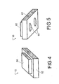
FIGURES 4 and 5 show perspective views of one of the light emitting chips of the package ofFIGURE 1 from two different vantage points. -
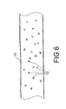
FIGURE 6 shows a cross-section of a portion of a solder mask suitable for use in the package ofFIGURE 1 . -
FIGURE 7 shows a cross-section of a portion of another solder mask suitable for use in the package ofFIGURE 1 . - With reference to
FIGURES 1-3 , a light emitting package 8 includes a plurality oflight emitting chips 10 disposed on a printedcircuit board 12. The illustrated printedcircuit board 12 includes an electrically insulatingboard 14, which in the illustrated embodiment includes aconductive metal core 16 and an insulatinglayer 18 made of a fiberglass resin or another electrically insulating material. In some embodiments, theconductive metal core 16 is omitted: for example, the electrically insulating board may be a fiberglass resin board without a metal core. Electrically conductive printed circuitry 20 (shown inFIGURE 3 ) is disposed on the insulatinglayer 18 of the insulatingboard 14. Asolder mask 22 is disposed on the insulatingboard 16 and includes openings or vias 24 (shown inFIGURE 3 ) through which thelight emitting chips 10 electrically contact the printedcircuitry 20. Optionally, one or more additional electronic components, such as the exampleelectronic component 26, are also disposed on the printedcircuit board 12 and electrically contact the printedcircuitry 20 by the openings orvias 24. - In the illustrated example, an
electronic component 26 receives electrical power through contact pins 30 and rectifies, converts, or otherwise conditions the received electrical power to produce operating power delivered to the printedcircuitry 20 to operate thelight emitting chips 10. Optionally, theelectronic component 26 or another electronic component can provide electrostatic discharge protection, selectable switching, or the like. Theelectronic component 26 can be embodied as an application-specific integrated circuit (ASIC), a programmed microcontroller or microprocessor, or the like. Alternatively or additionally, electronic components can be embodied by discrete components such as resistors, inductors, capacitors, op-amps, digital logic gates, or the like which are interconnected by the printed circuitry to perform power conditioning, switching, a light dimming function, or so forth. - In the illustrated embodiment, the electrically insulating
board 14 of the printedcircuit board 12 is a metal core board that includes the planarconductive metal core 16, such as an aluminum plate, copper foil, or the like, along with the insulatinglayer 18. The insulatinglayer 18 can be, for example, a fiberglass resin sheet or coating, which electrically isolates the printedcircuitry 20 from themetal core 16. Optionally, the printedcircuitry 20 electrically contacts themetal core 16 at selected points through vias (not shown) formed in the insulatinglayer 18, such that themetal core 16 acts as a ground plate for the printedcircuitry 20. Themetal core 16 also spreads and/or dissipates heat generated by thelight emitting chips 10 and the one or moreelectronic components 26. - The
light emitting chips 10, the one or moreelectronic components 26, and the printedcircuit board 12 are housed in a housing 36 (shown inFIGURE 1 ). Thehousing 36 includes sidewalls 38, 40 and a bottom 42 on which the printedcircuit board 12 is disposed. (One sidewall is omitted inFIGURE 1 to reveal the internal components of thelight emitting package 10; a second sidewall is disposed opposite the removed sidewall and is not visible in the perspective view ofFIGURE 1 ). Thesidewalls sidewalls circuit board 12. A top 48 of thehousing 36 faces thelight emitting chips 10 includes aphosphor plate 50. - In operation, the
light emitting chips 10 emit blue, violet, or ultraviolet light predominantly in a wavelength range between about 400 nanometers and about 470 nanometers. The emitted blue, violet, or ultraviolet light irradiates thephosphor plate 50. A phosphor disposed on or dispersed in thephosphor plate 50 emits fluorescence or phosphorescence predominantly in a wavelength range above 470 nanometers responsive to the blue, violet, or ultraviolet irradiation. Thephosphor plate 50 is light-transmissive for the fluorescence or phosphorescence so that the light emitting package 8 outputs light due to the fluorescence or phosphorescence. - In some embodiments, the phosphor includes one or more constituents that produce a white fluorescence or phosphorescence. In other embodiments the phosphor includes one or more constituents that produce fluorescence or phosphorescence of a selected color or blend of colors. Optionally, the
phosphor plate 50 is also light-transmissive for the blue, violet, or ultraviolet irradiation produced by thelight emitting chips 10, so that the light output of the light emitting package 8 is a combination of the fluorescence or phosphorescence output by the phosphor and direct light output by thelight emitting chips 10. For example, in some embodiments thelight emitting chips 10 produce blue emission light and the phosphor produces yellow light, so that the blended direct and phosphor-generated light combine in the output of the light emitting package 8 to approximate white light. The reflective interior surfaces 46 of thesidewalls light emitting chips 10 that impinges on thesidewalls phosphor plate 50 to improve light extraction efficiency. - In the illustrated embodiment, the
sidewall 40 includes electrically insulatedfeedthrough openings 52 through which the contact pins 30 of theelectronic component 26 pass to enable connection of an electrical power source to the light emitting package 8. Other power input configurations can also be used, such as a female power receptacle, a hard-wired electrical power cable, or the like. Optionally, a battery (not shown) is included in the light emitting package so that no external power supply is needed. - It will be appreciated that the
housing 36 is only an example. The housing can have other shapes besides rectangular, can include phosphorized sidewalls in addition to or in place of the phosphorized top, or can include other modifications. In some embodiments, the housing includes a phosphorized dome arranged over the light emitting chips. The light emitting package 8 can also include additional or other components, such as a heat sink, heat radiating fins, a lens or other optical component or components optically coupled with thephosphor plate 50, lensing for focusing the light emitting chip emission onto a phosphorized window or region, or so forth. - With continuing reference to
FIGURES 1-3 and with further reference toFIGURES 4 and 5 , each light emittingchip 10 can be a light emitting diode, a vertical cavity surface emitting laser (VCSEL), a monolithic array of light emitting diodes or lasers, an organic light emitting chip, or the like. In the illustrated embodiment, each light emittingchip 10 includes asemiconductor chip 60 flip-chip bonded to a sub-mount 62. The sub-mount 62 includes electrical vias electrically connecting thesemiconductor chip 60 withbackside bonding pads 64. The illustratedlight emitting chip 10 is only an example; in other embodiments the light emitting chip may be direct-bonded to the printedcircuit board 12 without a sub-mount, or may be bonded to a sub-mount but electrically contacted to the printed circuit board using wire bonds, or may be flip-chip bonded to bonding pads of a sub-mount which sub-mount bonding pads are electrically connected with the printedcircuit board 12 by wire bonds, or so forth. - In some embodiments, the light emitting chips are group III-nitride based light emitting diodes or lasers emitting light predominantly in a wavelength range between about 400 nanometers and about 470 nanometers. Other blue, violet, or ultraviolet light emitting chips can be employed which emit light predominantly in a wavelength range between about 400 nanometers and about 470 nanometers. In some embodiments, the electrical connections of the
light emitting chips 10 to the printedcircuit board 12 are produced by soldering. Thesolder mask 22 keeps the solder in the areas of thevias 24. In other embodiments, thermosonic bonding, thermocompressive bonding, or another bonding technique is used. Regardless of whether soldering or another bonding technique employed, thesolder mask 22 protects the printedcircuitry 20 from abrasion or other physical damage. - To maximize light extraction efficiency, the
solder mask 22 of the printedcircuit board 12 is constructed to have a reflectance of greater than 60% at least between about 400 nanometers and about 470 nanometers. In this way, the blue, violet, or ultraviolet light emitted by thelight emitting chips 10 which directly impinges upon the solder mask 22 (or which reflects off thesidewalls phosphor plate 50 and then impinges upon the solder mask 22) is substantially reflected toward thephosphor plate 50 to contribute to generation of phosphorescence or fluorescence. In some preferred embodiments, thesolder mask 22 of the printedcircuit board 12 is constructed to have a reflectance of greater than about 85% at least between about 400 nanometers and about 470 nanometers. In some preferred embodiments, thesolder mask 22 of the printedcircuit board 12 is constructed to have a reflectance of greater than about 85% at least between about 400 nanometers and about 740 nanometers, so that thesolder mask 22 also reflects phosphorescence or fluorescence generated by the irradiated phosphor that is directed toward the printedcircuit board 12. In some preferred embodiments, thesolder mask 22 of the printedcircuit board 12 is constructed to have a reflectance of greater than about 85% at least between about 400 nanometers and an upper wavelength substantially spanning the wavelength range of light emitted by the phosphor (for example, at least up to an upper wavelength of 650 nanometers for an example phosphor emitting light predominantly in a wavelength range of 500-650 nanometers). - With reference to
FIGURE 6 , in some embodiments, the electrically insulatingsolder mask 22 is formed of a film of photostabilized electrically insulatingbinder material 70, such as a photosensitive epoxy, a photosensitive polyimide, or so forth, in which particles of areflective filler material 72 are dispersed. The particles ofreflective filler material 72 can be, for example, a titanium oxide (such as titanium dioxide, TiO2), an aluminum oxide (such as alumina, Al2O3), a high-refractive index glass, or so forth. The concentration offiller material 72 in thebinder material 70 as well as the mean particle size, average particle shape, and so forth are selected to provide adequate reflectance for thesolder mask 22. An electrically conductive filler material can be employed if its concentration is dilute enough to retain the substantially electrically insulating characteristic of thesolder mask 22. - In one example, in which the binder material is a negative photosensitive epoxy, the
solder mask 22 is constructed as follows. The constituents of the photosensitive epoxy are combined with thefiller material 72 to generate a liquid photosensitive epoxy source material, which is disposed on the electrically insulatingboard 14 as a film. Suitable deposition methods include spray coating, curtain coating, or so forth. Depending upon the type of epoxy, a soft cure may be performed to partially harden or solidify the photosensitive epoxy film. Soft curing is not employed with some types of epoxy, however. These processes are performed in a yellow-lighted photolithography room or other environment whose ambient illumination does not activate the photosensitive epoxy. - The
vias 24 of thesolder mask 22 are then formed by optically exposing the photosensitive epoxy film through a photo-mask that blocks light exposure in the areas of thevias 24. The optically exposed photosensitive epoxy film is developed using suitable chemicals which remove only those areas of the photosensitive epoxy film which have not been exposed to light; thus, the areas of the vias 24 which were blocked from light exposure are removed to open up thevias 24. Those areas which were exposed to light are photostabilized and are not removed by the developer chemical or chemicals. Depending upon the type of photosensitive epoxy, a hard cure may be performed to further solidify or harden the photostabilized epoxy film. - In some embodiments, the concentration of
filler material 72 is low enough so that incorporation of thefiller material 72 does not significantly alter the photosensitive characteristics of thephotosensitive binder material 70. In other embodiments, incorporation of thefiller material 72 reduces the photosensitivity of thephotosensitive binder material 70. In these embodiments, the amount of photosensitizer in thephotosensitive binder material 70 can be increased to counteract the effect of thefiller material 72, or the light exposure and/or developing time can be increased to account for the reduced photosensitivity. Typically, thesolder mask 22 is between about twelve microns and seventy-five microns thick. For a relatively thicker solder mask, the concentration of thefiller material 72 can generally be reduced while retaining the desired reflectance. Filler materials such as TiO2 or Al2O3 exhibit reflectances greater than about 85% to 90% at least down to 400 nanometers, and more typically at least down to about 350 nanometers. Hence, for sufficiently high concentrations offiller material 72, the reflectance of thesolder mask 22 can be increased to above 60% or above 85% (depending upon the filler concentration, reflectance characteristics of the particles, and so forth) in the wavelength range between about 400 nanometers and about 470 nanometers. - With reference to
FIGURE 7 , in some embodiments, the electrically insulatingsolder mask 22 is formed of a multiple-layer specular reflector sheet 80. Openings are cut into the sheet 80 to define thevias 24, for example using laser cutting, mechanical punching, or so forth, and the multiple-layer specular reflector sheet 80 is glued or otherwise secured to the electrically insulatingboard 14. The reflector sheet 80 includes a stack of reflective dielectric layers including alternating layers of dielectric material having different refractive indices, different birefringence characteristics, or other dissimilar optical characteristics. The thicknesses and optical characteristics of the layers are selected to provide a high stack reflectance in the wavelength range between about 400 nanometers and about 470 nanometers, and preferably in the wavelength range between about 400 nanometers and about 740 nanometers. - In some embodiments, the multiple-layer specular reflector sheet 80 is a commercially available reflector sheet, such as a VM2000 reflector film or a Vikuiti™ enhanced specular reflector film or a (available from 3M, St. Paul, MN). Solder masks formed of VM2000 or Vikuiti™ enhanced specular reflector films have been measured by the inventors to have reflectances greater than 85% between 400 nanometers and 740 nanometers, with these high reflectances being observed for both front and back sides of the film. In contrast, a conventional white solder mask was measured to have reflectances of about 80% in the visible, reflectances of less than about 70% for wavelengths below about 430 nanometers, and reflectances of less than 60% for wavelengths below about 410 nanometers.
- The light emitting package 8 produces visible light through wavelength conversion by the
phosphor plate 50. In other contemplated embodiments, the light emitting package is a blue, violet, or ultraviolet light source that emits the direct light produced by the light emitting chips predominantly in the wavelength range between about 400 nanometers and about 470 nanometers. In these embodiments, optics, sidewalls, lenses, cover glasses, or so forth will generally reflect or otherwise redirect some of the direct light predominantly in the wavelength range between about 400 nanometers and about 470 nanometers toward the solder mask of the printed circuit board. Hence, the solder masks disclosed herein which are highly reflective at least between about 400 nanometers and about 470 nanometers are also advantageous in these blue, violet, or ultraviolet light sources that do not employ phosphor. - The invention has been described with reference to the preferred embodiments. Obviously, modifications and alterations will occur to others upon reading and understanding the preceding detailed description. It is intended that the invention be construed as including all such modifications and alterations insofar as they come within the scope of the appended claims or the equivalents thereof.
- The appended claims follow:
Claims (10)
- A light emitting apparatus (8) comprising:one or more light emitting chips (10) emitting light; anda printed circuit board (12) on which the one or more light emitting chips (10) are disposed, the printed circuit board (12) including: (i) an electrically insulating board (14), (ii) electrically conductive printed circuitry (20), and (iii) an electrically insulating solder mask (22) having vias through which the one or more light emitting chips (10) electrically contact the printed circuitry (20), the solder mask (22) having a reflectance of greater than 60% at least between about 400 nanometers and about 470 nanometers, the solder mask (22) including an electrically insulating binder (70) material and a filler material (72) dispersed in the binder material (70), the filler material (72) having reflectance greater than about 85% of the emitted light.
- The light emitting apparatus (8) as set forth in claim 1, further comprising:a housing (36) inside of which the one or more light emitting chips (10) and the printed circuit board (12) are disposed, the housing (36) including a phosphor (50) arranged to be irradiated by the one or more light emitting chips (10) and emitting light in a wavelength range predominantly above 470 nanometers responsive to the irradiating, the phosphor (50) and the printed circuit board (12) being relatively arranged such that at least some of the light emitted by the one or more light emitting chips (10) predominantly in the wavelength range between about 400 nanometers and about 470 nanometers reflects from the phosphor (50) onto the solder mask (22) of the printed circuit board (12).
- The light emitting apparatus (8) as set forth in claim 3, wherein the solder mask (22) has a reflectance greater than 85% at least between about 400 nanometers and about 470 nanometers.
- The light emitting apparatus (8) as set forth in one of the preceding claims, wherein the electrically insulating binder (70) material is a photostabilized material.
- The light emitting apparatus (8) as set forth in one of the preceding claims, wherein the filler material (72) is one of a titanium oxide and an aluminum oxide.
- The light emitting apparatus (8) as set forth in one of the preceding claims, wherein the electrically insulating board (14) comprises:a metal layer (16); andan electrically insulating layer (18) disposed on at least one side of the metal layer (16), the printed circuitry (20) being disposed on the electrically insulating layer (18).
- A light emitting apparatus (8) comprising:one or more light emitting chips (10) emitting light predominantly in a wavelength range between about 400 nanometers and about 470 nanometers; anda printed circuit board (14) on which the one or more light emitting chips (10) are disposed, the printed circuit board (14) including: (i) an electrically insulating board (14), (ii) electrically conductive printed circuitry (20), and (iii) an electrically insulating solder mask (22) comprising a multiple-layer specular reflector sheet (80) and having vias through which the one or more light emitting chips (10) electrically contact the printed circuitry (20), the solder mask (22) having a reflectance of greater than 60% at least between about 400 nanometers and about 470 nanometers.
- The light emitting apparatus (8) as set forth in claim 7, wherein the multiple-layer specular reflector (80) sheet comprises:a stack of reflective dielectric layers formed of alternating layers of dielectric material having different refractive indices, different birefringence characteristics, or other dissimilar optical characteristics.
- The light emitting apparatus as set forth in claim 7, further comprising:a phosphor (50) arranged to be irradiated by the one or more light emitting chips (10) and emitting light in a wavelength range predominantly above 470 nanometers responsive to the irradiating, the phosphor (50) and the printed circuit board (12) being relatively arranged such that at least some of the light emitted by the one or more light emitting chips (10) predominantly in the wavelength range between about 400 nanometers and about 470 nanometers reflects from the phosphor (50) onto the solder mask (22) of the printed circuit board (12).
- A method for fabricating a light emitting apparatus (8), the method comprising:providing an electrically insulating board (14) with electrically conductive printed circuitry (20) disposed thereon;disposing an electrically insulating solder mask (22) having a reflectance of greater than 60% at least between about 400 nanometers and about 470 nanometers on the electrically insulating board (14) by combining constituents of a photosensitive epoxy (70) with a reflective filler (72) to generate epoxy source material, the reflective filler (72) material having a reflectance greater than about 85% at least between about 400 nanometers and about 470 nanometers, disposing the epoxy source material on the electrically insulating board (14) to define an epoxy solder mask layer and photolithographically forming the vias accessing the printed circuitry in the epoxy solder mask layer; and.disposing one or more light emitting chips (10) on the insulating solder mask (22), the one or more light emitting chips (10) electrically contacting the printed circuitry (20) through the vias in the solder mask (22), the one or more light emitting chips (10) emitting light predominantly in a wavelength range between about 400 nanometers and about 470 nanometers.
Applications Claiming Priority (2)
| Application Number | Priority Date | Filing Date | Title |
|---|---|---|---|
| US10/891,722 US7201497B2 (en) | 2004-07-15 | 2004-07-15 | Led lighting system with reflective board |
| PCT/US2005/024664 WO2006019730A2 (en) | 2004-07-15 | 2005-07-13 | Led lighting system with reflective board |
Publications (3)
| Publication Number | Publication Date |
|---|---|
| EP1781984A2 EP1781984A2 (en) | 2007-05-09 |
| EP1781984A4 EP1781984A4 (en) | 2012-05-30 |
| EP1781984B1 true EP1781984B1 (en) | 2014-10-15 |
Family
ID=35599198
Family Applications (1)
| Application Number | Title | Priority Date | Filing Date |
|---|---|---|---|
| EP05771031.1A Expired - Lifetime EP1781984B1 (en) | 2004-07-15 | 2005-07-13 | Led lighting system with reflective board |
Country Status (6)
| Country | Link |
|---|---|
| US (2) | US7201497B2 (en) |
| EP (1) | EP1781984B1 (en) |
| JP (1) | JP2008507135A (en) |
| CN (1) | CN101018974B (en) |
| DK (1) | DK1781984T3 (en) |
| WO (1) | WO2006019730A2 (en) |
Families Citing this family (110)
| Publication number | Priority date | Publication date | Assignee | Title |
|---|---|---|---|---|
| US10340424B2 (en) | 2002-08-30 | 2019-07-02 | GE Lighting Solutions, LLC | Light emitting diode component |
| JP4568133B2 (en) * | 2004-03-30 | 2010-10-27 | 三洋電機株式会社 | Semiconductor laser device and optical device |
| JP4062703B2 (en) * | 2004-04-28 | 2008-03-19 | スタンレー電気株式会社 | Lighting unit |
| JP2007081234A (en) * | 2005-09-15 | 2007-03-29 | Toyoda Gosei Co Ltd | Lighting device |
| EP1996860A2 (en) * | 2006-01-31 | 2008-12-03 | 3M Innovative Properties Company | Led illumination assembly with compliant foil construction |
| US7710045B2 (en) * | 2006-03-17 | 2010-05-04 | 3M Innovative Properties Company | Illumination assembly with enhanced thermal conductivity |
| US7824075B2 (en) * | 2006-06-08 | 2010-11-02 | Lighting Science Group Corporation | Method and apparatus for cooling a lightbulb |
| US7842960B2 (en) * | 2006-09-06 | 2010-11-30 | Lumination Llc | Light emitting packages and methods of making same |
| KR20080037269A (en) * | 2006-10-25 | 2008-04-30 | 엘지전자 주식회사 | Refrigerator Lighting |
| TW200821694A (en) * | 2006-11-01 | 2008-05-16 | Au Optronics Corp | Reflective light source device and manufacture method thereof |
| US9178121B2 (en) * | 2006-12-15 | 2015-11-03 | Cree, Inc. | Reflective mounting substrates for light emitting diodes |
| US7806560B2 (en) * | 2007-01-31 | 2010-10-05 | 3M Innovative Properties Company | LED illumination assembly with compliant foil construction |
| JP4945264B2 (en) * | 2007-02-26 | 2012-06-06 | 三洋電機株式会社 | Open showcase |
| US20080203948A1 (en) * | 2007-02-27 | 2008-08-28 | Unity Opto Technology Co., Ltd. | Lighting device |
| WO2008125672A1 (en) * | 2007-04-16 | 2008-10-23 | Goodrich Lighting Systems Gmbh | Color-variable led light, particularly for lighting the interior of vehicles |
| US8449143B2 (en) * | 2007-05-18 | 2013-05-28 | Denki Kagaku Kogyo Kabushiki Kaisha | Metal base circuit board |
| TWI452716B (en) * | 2007-06-08 | 2014-09-11 | Formosa Epitaxy Inc | Gallium nitride based light emitting diode and manufacturing method thereof |
| WO2009000282A1 (en) * | 2007-06-22 | 2008-12-31 | Lioris B.V. | High voltage led lighting system |
| WO2009042303A1 (en) * | 2007-08-13 | 2009-04-02 | Everhart Robert L | Solid-state lighting fixtures |
| US20090086484A1 (en) * | 2007-09-28 | 2009-04-02 | Johnson Stephen G | Small form factor downlight system |
| KR101345384B1 (en) * | 2007-11-16 | 2013-12-24 | 삼성전자주식회사 | light guide plate, lighting apparatus using the plate and fabrication method of the plate |
| US8042976B2 (en) * | 2007-11-30 | 2011-10-25 | Taiyo Holdings Co., Ltd. | White hardening resin composition, hardened material, printed-wiring board and reflection board for light emitting device |
| US8118447B2 (en) | 2007-12-20 | 2012-02-21 | Altair Engineering, Inc. | LED lighting apparatus with swivel connection |
| US7712918B2 (en) | 2007-12-21 | 2010-05-11 | Altair Engineering , Inc. | Light distribution using a light emitting diode assembly |
| US7717591B2 (en) * | 2007-12-27 | 2010-05-18 | Lumination Llc | Incorporating reflective layers into LED systems and/or components |
| JP5432922B2 (en) * | 2008-01-22 | 2014-03-05 | コーニンクレッカ フィリップス エヌ ヴェ | Illumination device comprising an LED and a transmissive support having a luminescent material |
| AT506384B1 (en) * | 2008-02-07 | 2013-05-15 | Schrutek Elmar Ing | LIGHTING EQUIPMENT |
| US8360599B2 (en) | 2008-05-23 | 2013-01-29 | Ilumisys, Inc. | Electric shock resistant L.E.D. based light |
| KR101518457B1 (en) * | 2008-06-12 | 2015-05-12 | 서울반도체 주식회사 | Flexible printed circuit board for light emitting diode mounting |
| US7976196B2 (en) | 2008-07-09 | 2011-07-12 | Altair Engineering, Inc. | Method of forming LED-based light and resulting LED-based light |
| US7946729B2 (en) | 2008-07-31 | 2011-05-24 | Altair Engineering, Inc. | Fluorescent tube replacement having longitudinally oriented LEDs |
| US8674626B2 (en) | 2008-09-02 | 2014-03-18 | Ilumisys, Inc. | LED lamp failure alerting system |
| US8256924B2 (en) | 2008-09-15 | 2012-09-04 | Ilumisys, Inc. | LED-based light having rapidly oscillating LEDs |
| US7938562B2 (en) | 2008-10-24 | 2011-05-10 | Altair Engineering, Inc. | Lighting including integral communication apparatus |
| US8653984B2 (en) | 2008-10-24 | 2014-02-18 | Ilumisys, Inc. | Integration of LED lighting control with emergency notification systems |
| US8444292B2 (en) | 2008-10-24 | 2013-05-21 | Ilumisys, Inc. | End cap substitute for LED-based tube replacement light |
| US8901823B2 (en) | 2008-10-24 | 2014-12-02 | Ilumisys, Inc. | Light and light sensor |
| US8214084B2 (en) | 2008-10-24 | 2012-07-03 | Ilumisys, Inc. | Integration of LED lighting with building controls |
| US8324817B2 (en) | 2008-10-24 | 2012-12-04 | Ilumisys, Inc. | Light and light sensor |
| JP4572994B2 (en) * | 2008-10-28 | 2010-11-04 | 東芝ライテック株式会社 | Light emitting module and lighting device |
| US8556452B2 (en) | 2009-01-15 | 2013-10-15 | Ilumisys, Inc. | LED lens |
| US8362710B2 (en) | 2009-01-21 | 2013-01-29 | Ilumisys, Inc. | Direct AC-to-DC converter for passive component minimization and universal operation of LED arrays |
| US8664880B2 (en) | 2009-01-21 | 2014-03-04 | Ilumisys, Inc. | Ballast/line detection circuit for fluorescent replacement lamps |
| CN102369166B (en) * | 2009-02-26 | 2014-11-26 | 康宁股份有限公司 | Apparatus for forming glass with edge directors and methods |
| DE202009018419U1 (en) * | 2009-03-09 | 2011-08-17 | Tridonic Jennersdorf Gmbh | LED module with improved light output |
| US20100245259A1 (en) * | 2009-03-25 | 2010-09-30 | Honeywell International Inc. | Small screen display with a data filtering and sorting user interface |
| DE102009019412A1 (en) * | 2009-04-29 | 2010-11-04 | Fa. Austria Technologie & Systemtechnik Ag | Method for producing a printed circuit board with LEDs and printed reflector surface and printed circuit board, produced by the method |
| US8184230B2 (en) * | 2009-05-08 | 2012-05-22 | Honeywell International Inc. | High efficiency backlight assembly for flat panel display assembly and method for the manufacture thereof |
| US8330381B2 (en) | 2009-05-14 | 2012-12-11 | Ilumisys, Inc. | Electronic circuit for DC conversion of fluorescent lighting ballast |
| US8299695B2 (en) | 2009-06-02 | 2012-10-30 | Ilumisys, Inc. | Screw-in LED bulb comprising a base having outwardly projecting nodes |
| CA2765200A1 (en) | 2009-06-23 | 2011-01-13 | Altair Engineering, Inc. | Illumination device including leds and a switching power control system |
| KR20120079470A (en) * | 2009-09-25 | 2012-07-12 | 오스람 옵토 세미컨덕터스 게엠베하 | Semiconductor lighting fixtures |
| US8593040B2 (en) | 2009-10-02 | 2013-11-26 | Ge Lighting Solutions Llc | LED lamp with surface area enhancing fins |
| JP5258978B2 (en) * | 2010-01-12 | 2013-08-07 | シャープ株式会社 | LED substrate, backlight unit, and liquid crystal display device |
| TWM393643U (en) * | 2010-01-15 | 2010-12-01 | Idolite Technology Corp | LED device with coating structure |
| US9631782B2 (en) * | 2010-02-04 | 2017-04-25 | Xicato, Inc. | LED-based rectangular illumination device |
| WO2011119921A2 (en) | 2010-03-26 | 2011-09-29 | Altair Engineering, Inc. | Led light with thermoelectric generator |
| CA2794512A1 (en) | 2010-03-26 | 2011-09-29 | Ilumisys, Inc. | Led light tube with dual sided light distribution |
| WO2011119958A1 (en) | 2010-03-26 | 2011-09-29 | Altair Engineering, Inc. | Inside-out led bulb |
| US8454193B2 (en) | 2010-07-08 | 2013-06-04 | Ilumisys, Inc. | Independent modules for LED fluorescent light tube replacement |
| CA2803267A1 (en) | 2010-07-12 | 2012-01-19 | Ilumisys, Inc. | Circuit board mount for led light tube |
| US8853723B2 (en) | 2010-08-18 | 2014-10-07 | E. I. Du Pont De Nemours And Company | Light emitting diode assembly and thermal control blanket and methods relating thereto |
| TW201208879A (en) | 2010-08-18 | 2012-03-01 | Du Pont | Light emitting diode assembly and thermal control blanket and methods relating thereto |
| US8506105B2 (en) | 2010-08-25 | 2013-08-13 | Generla Electric Company | Thermal management systems for solid state lighting and other electronic systems |
| DE102010047376A1 (en) * | 2010-10-05 | 2012-04-05 | Gm Global Technology Operations Llc (N.D.Ges.D. Staates Delaware) | Automotive headlamp |
| EP2633227B1 (en) | 2010-10-29 | 2018-08-29 | iLumisys, Inc. | Mechanisms for reducing risk of shock during installation of light tube |
| US20130228276A1 (en) * | 2010-11-10 | 2013-09-05 | Kuo-Kuang Chang | Method for manufacturing cover plate and method for manufacturing encapsulated light-emitting diode using the cover plate |
| US20150062915A1 (en) * | 2013-09-05 | 2015-03-05 | Cree, Inc. | Light emitting diode devices and methods with reflective material for increased light output |
| US8870415B2 (en) | 2010-12-09 | 2014-10-28 | Ilumisys, Inc. | LED fluorescent tube replacement light with reduced shock hazard |
| KR101167461B1 (en) * | 2010-12-27 | 2012-07-31 | 삼성전기주식회사 | Laser Navigation Module |
| KR101913878B1 (en) | 2010-12-29 | 2018-10-31 | 쓰리엠 이노베이티브 프로퍼티즈 컴파니 | Phosphor reflector assembly for remote phosphor led device |
| US20120199386A1 (en) * | 2011-02-04 | 2012-08-09 | Ibiden Co., Ltd. | Multilayer printed wiring board |
| CN103404240B (en) * | 2011-03-03 | 2017-09-08 | 飞利浦照明控股有限公司 | circuit board assembly |
| US20120229990A1 (en) * | 2011-03-08 | 2012-09-13 | Ibiden Co., Ltd. | Multilayer printed wiring board and method for manufacturing multilayer printed wiring board |
| EP2500623A1 (en) | 2011-03-18 | 2012-09-19 | Koninklijke Philips Electronics N.V. | Method for providing a reflective coating to a substrate for a light-emitting device |
| WO2013028965A2 (en) | 2011-08-24 | 2013-02-28 | Ilumisys, Inc. | Circuit board mount for led light |
| JP2013153068A (en) | 2012-01-25 | 2013-08-08 | Shinko Electric Ind Co Ltd | Wiring board, light emitting device, and manufacturing method of wiring board |
| JP5848976B2 (en) | 2012-01-25 | 2016-01-27 | 新光電気工業株式会社 | WIRING BOARD, LIGHT EMITTING DEVICE, AND WIRING BOARD MANUFACTURING METHOD |
| RU2612563C2 (en) * | 2012-01-25 | 2017-03-09 | Филипс Лайтинг Холдинг Б.В. | Led module and lamp containing said module |
| JP6096413B2 (en) * | 2012-01-25 | 2017-03-15 | 新光電気工業株式会社 | WIRING BOARD, LIGHT EMITTING DEVICE, AND WIRING BOARD MANUFACTURING METHOD |
| JP6230777B2 (en) * | 2012-01-30 | 2017-11-15 | 新光電気工業株式会社 | WIRING BOARD, WIRING BOARD MANUFACTURING METHOD, AND LIGHT EMITTING DEVICE |
| US9184518B2 (en) | 2012-03-02 | 2015-11-10 | Ilumisys, Inc. | Electrical connector header for an LED-based light |
| TWM443813U (en) * | 2012-03-06 | 2012-12-21 | Winsky Technology Ltd | Illumination device |
| US9500355B2 (en) | 2012-05-04 | 2016-11-22 | GE Lighting Solutions, LLC | Lamp with light emitting elements surrounding active cooling device |
| EP2870405A4 (en) | 2012-07-06 | 2015-11-25 | Ge Lighting Solutions Llc | Linear light fixture |
| WO2014008463A1 (en) | 2012-07-06 | 2014-01-09 | Ilumisys, Inc. | Power supply assembly for led-based light tube |
| US9271367B2 (en) | 2012-07-09 | 2016-02-23 | Ilumisys, Inc. | System and method for controlling operation of an LED-based light |
| JP2014063600A (en) * | 2012-09-20 | 2014-04-10 | Mitsubishi Electric Corp | Linear light source device |
| US9285084B2 (en) | 2013-03-14 | 2016-03-15 | Ilumisys, Inc. | Diffusers for LED-based lights |
| DE202013101823U1 (en) * | 2013-04-26 | 2014-07-29 | Zumtobel Lighting Gmbh | Plate-shaped reflector element for LED board |
| KR101510938B1 (en) * | 2013-05-09 | 2015-04-17 | 주식회사 올릭스 | Plate type led lighting device |
| US9267650B2 (en) | 2013-10-09 | 2016-02-23 | Ilumisys, Inc. | Lens for an LED-based light |
| WO2015112437A1 (en) | 2014-01-22 | 2015-07-30 | Ilumisys, Inc. | Led-based light with addressed leds |
| US9510400B2 (en) | 2014-05-13 | 2016-11-29 | Ilumisys, Inc. | User input systems for an LED-based light |
| CN105221975A (en) * | 2014-06-17 | 2016-01-06 | 深圳市斯迈得光电子有限公司 | A kind of remote excitation technical pattern LED light source |
| DE102014110960A1 (en) * | 2014-08-01 | 2016-02-04 | GOM - Gesellschaft für Optische Meßtechnik mbH | Measuring device for the three-dimensional optical measurement of objects with a topometric sensor and use of a multi-laser chip component |
| JP6361385B2 (en) * | 2014-09-04 | 2018-07-25 | 日亜化学工業株式会社 | Circuit board and light emitting device using the same |
| CN104470310B (en) * | 2014-12-04 | 2017-07-28 | 天水华天微电子股份有限公司 | The assembly method of Switching Power Supply pin configuration and Switching Power Supply lead |
| CN205790070U (en) * | 2015-01-20 | 2016-12-07 | 现代摩比斯株式会社 | Encapsulate for the LED of car light |
| KR102352411B1 (en) * | 2015-01-20 | 2022-01-18 | 현대모비스 주식회사 | LED package for ramp of vehicle |
| WO2016142258A1 (en) * | 2015-03-11 | 2016-09-15 | Koninklijke Philips N.V. | Light emitting device cooling |
| US10161568B2 (en) | 2015-06-01 | 2018-12-25 | Ilumisys, Inc. | LED-based light with canted outer walls |
| CN106369367A (en) * | 2015-07-23 | 2017-02-01 | 晶元光电股份有限公司 | Light emitting device |
| US10211188B2 (en) * | 2016-12-01 | 2019-02-19 | Cheng Chang TransFlexDisplay Corp. | Method for making an LED module and module made thereof |
| CN113707036A (en) * | 2020-05-22 | 2021-11-26 | 北京芯海视界三维科技有限公司 | Light-emitting module, display screen and display |
| US11526051B2 (en) | 2021-04-16 | 2022-12-13 | Apple Inc. | Displays with direct-lit backlight units |
| US11592706B2 (en) | 2021-04-16 | 2023-02-28 | Apple Inc. | Displays with direct-lit backlight units |
| US11513392B1 (en) | 2021-09-23 | 2022-11-29 | Apple Inc. | Direct-lit backlight units with optical films |
| CN114583022B (en) * | 2022-03-25 | 2024-10-18 | 扬州大学广陵学院 | A method for manufacturing a micro display light-emitting module |
| JPWO2025047658A1 (en) * | 2023-08-29 | 2025-03-06 |
Family Cites Families (31)
| Publication number | Priority date | Publication date | Assignee | Title |
|---|---|---|---|---|
| GB950475A (en) * | 1958-11-19 | 1964-02-26 | Ass Elect Ind | Improvements in electric discharge lamps |
| JPS6284024A (en) * | 1985-10-09 | 1987-04-17 | Ichimaru Fuarukosu Kk | Fibroblast cell proliferation promoting agent extracted from hydrolyzed fiber of connective tissue |
| JPS6375057A (en) * | 1986-09-19 | 1988-04-05 | Showa Denko Kk | Resin mixture |
| US6210862B1 (en) * | 1989-03-03 | 2001-04-03 | International Business Machines Corporation | Composition for photoimaging |
| US5122905A (en) | 1989-06-20 | 1992-06-16 | The Dow Chemical Company | Relective polymeric body |
| US5094788A (en) | 1990-12-21 | 1992-03-10 | The Dow Chemical Company | Interfacial surface generator |
| US5269995A (en) | 1992-10-02 | 1993-12-14 | The Dow Chemical Company | Coextrusion of multilayer articles using protective boundary layers and apparatus therefor |
| US5389324A (en) | 1993-06-07 | 1995-02-14 | The Dow Chemical Company | Layer thickness gradient control in multilayer polymeric bodies |
| US5882774A (en) | 1993-12-21 | 1999-03-16 | Minnesota Mining And Manufacturing Company | Optical film |
| US6101032A (en) | 1994-04-06 | 2000-08-08 | 3M Innovative Properties Company | Light fixture having a multilayer polymeric film |
| JP3329573B2 (en) * | 1994-04-18 | 2002-09-30 | 日亜化学工業株式会社 | LED display |
| US5699188A (en) | 1995-06-26 | 1997-12-16 | Minnesota Mining And Manufacturing Co. | Metal-coated multilayer mirror |
| US6080467A (en) | 1995-06-26 | 2000-06-27 | 3M Innovative Properties Company | High efficiency optical devices |
| US5785404A (en) | 1995-06-29 | 1998-07-28 | Siemens Microelectronics, Inc. | Localized illumination device |
| US5976424A (en) | 1996-07-31 | 1999-11-02 | Minnesota Mining And Manufacturing Company | Method for making multilayer optical films having thin optical layers |
| JPH1152570A (en) * | 1997-08-05 | 1999-02-26 | Mitsui Chem Inc | Photosensitive resin composition |
| US6157490A (en) | 1998-01-13 | 2000-12-05 | 3M Innovative Properties Company | Optical film with sharpened bandedge |
| CN1170189C (en) * | 1998-09-25 | 2004-10-06 | 时至准钟表股份有限公司 | Liquid crystal display device |
| US6208466B1 (en) | 1998-11-25 | 2001-03-27 | 3M Innovative Properties Company | Multilayer reflector with selective transmission |
| US6222207B1 (en) * | 1999-05-24 | 2001-04-24 | Lumileds Lighting, U.S. Llc | Diffusion barrier for increased mirror reflectivity in reflective solderable contacts on high power LED chip |
| US6161910A (en) * | 1999-12-14 | 2000-12-19 | Aerospace Lighting Corporation | LED reading light |
| EP1393374B1 (en) * | 2001-05-26 | 2016-08-24 | GE Lighting Solutions, LLC | High power led lamp for spot illumination |
| JP2002374007A (en) * | 2001-06-15 | 2002-12-26 | Toyoda Gosei Co Ltd | Light emitting device |
| JP3760900B2 (en) * | 2001-09-06 | 2006-03-29 | セイコーエプソン株式会社 | Light guiding device, electro-optical device, and electronic apparatus |
| JP2003177528A (en) * | 2001-09-21 | 2003-06-27 | Tamura Kaken Co Ltd | Photosensitive resin composition and printed wiring board |
| JP4006578B2 (en) * | 2002-03-22 | 2007-11-14 | サンユレック株式会社 | Method for manufacturing two side-emitting LEDs |
| US20030193055A1 (en) | 2002-04-10 | 2003-10-16 | Martter Robert H. | Lighting device and method |
| US6945672B2 (en) | 2002-08-30 | 2005-09-20 | Gelcore Llc | LED planar light source and low-profile headlight constructed therewith |
| JP2004119634A (en) * | 2002-09-25 | 2004-04-15 | Toshiba Lighting & Technology Corp | Light emitting device |
| DE60319266D1 (en) | 2002-11-19 | 2008-04-03 | Dan Friis | LIGHT BODY OR LIGHT SOURCE BASED ON LUMINAIRE DIODES |
| WO2004100226A2 (en) * | 2003-05-05 | 2004-11-18 | Gelcore Llc | Method and apparatus for led panel lamp systems |
-
2004
- 2004-07-15 US US10/891,722 patent/US7201497B2/en not_active Expired - Lifetime
-
2005
- 2005-07-13 CN CN2005800309226A patent/CN101018974B/en not_active Expired - Lifetime
- 2005-07-13 WO PCT/US2005/024664 patent/WO2006019730A2/en not_active Ceased
- 2005-07-13 DK DK05771031.1T patent/DK1781984T3/en active
- 2005-07-13 EP EP05771031.1A patent/EP1781984B1/en not_active Expired - Lifetime
- 2005-07-13 JP JP2007521562A patent/JP2008507135A/en active Pending
-
2007
- 2007-03-19 US US11/725,410 patent/US7431479B2/en not_active Expired - Lifetime
Also Published As
| Publication number | Publication date |
|---|---|
| JP2008507135A (en) | 2008-03-06 |
| WO2006019730A3 (en) | 2006-04-20 |
| US20070165402A1 (en) | 2007-07-19 |
| WO2006019730A2 (en) | 2006-02-23 |
| EP1781984A4 (en) | 2012-05-30 |
| DK1781984T3 (en) | 2015-01-12 |
| EP1781984A2 (en) | 2007-05-09 |
| US7201497B2 (en) | 2007-04-10 |
| CN101018974B (en) | 2010-08-25 |
| CN101018974A (en) | 2007-08-15 |
| US20060012991A1 (en) | 2006-01-19 |
| US7431479B2 (en) | 2008-10-07 |
Similar Documents
| Publication | Publication Date | Title |
|---|---|---|
| DK1781984T3 (en) | Led lighting system with reflecting plate | |
| US7717591B2 (en) | Incorporating reflective layers into LED systems and/or components | |
| US11393949B2 (en) | Semiconductor component and illumination device | |
| JP6831801B2 (en) | Light emitting diode chip with distributed Bragg reflector | |
| CN113237032B (en) | Light source device and lighting device | |
| JP4172196B2 (en) | Light emitting diode | |
| KR101114487B1 (en) | Light Emitting Device | |
| CN1327579C (en) | light emitting device | |
| KR101297405B1 (en) | Light emitting device employing dielectric multilayer reflecting mirror | |
| US7872280B2 (en) | Semiconductor light emitting device, method of manufacturing the same, and lighting apparatus and display apparatus using the same | |
| JP6089686B2 (en) | Light emitting device | |
| US20120098015A1 (en) | Optoelectronic semiconductor component | |
| TWI648869B (en) | Illuminating device | |
| JP4116960B2 (en) | Semiconductor light emitting device, light emitting module, lighting device, and method for manufacturing semiconductor light emitting device | |
| JP2007059864A (en) | LIGHTING DEVICE AND LIGHT EMITTING DIODE DEVICE | |
| CN110440149B (en) | light-emitting device | |
| KR20140045655A (en) | A light emitting device package | |
| JP2008159708A (en) | Light-emitting device | |
| KR101367378B1 (en) | Light emitting device employing dielectric multilayer reflecting mirror | |
| JP5484544B2 (en) | Light emitting device | |
| KR101797968B1 (en) | Light Emitting Device Package | |
| KR101258228B1 (en) | Light emitting device having plurality of light-converting material laters | |
| JP5085851B2 (en) | Light emitting device and lighting device | |
| KR101904263B1 (en) | Light Emitting Device Package | |
| KR101258232B1 (en) | Light emitting device having plurality of light-converting material layers |
Legal Events
| Date | Code | Title | Description |
|---|---|---|---|
| PUAI | Public reference made under article 153(3) epc to a published international application that has entered the european phase |
Free format text: ORIGINAL CODE: 0009012 |
|
| 17P | Request for examination filed |
Effective date: 20070205 |
|
| AK | Designated contracting states |
Kind code of ref document: A2 Designated state(s): AT BE BG CH CY CZ DE DK EE ES FI FR GB GR HU IE IS IT LI LT LU LV MC NL PL PT RO SE SI SK TR |
|
| DAX | Request for extension of the european patent (deleted) | ||
| RAP1 | Party data changed (applicant data changed or rights of an application transferred) |
Owner name: LUMINATION, LLC |
|
| RAP1 | Party data changed (applicant data changed or rights of an application transferred) |
Owner name: GE LIGHTING SOLUTIONS, LLC |
|
| A4 | Supplementary search report drawn up and despatched |
Effective date: 20120426 |
|
| RIC1 | Information provided on ipc code assigned before grant |
Ipc: H01S 5/40 20060101ALI20120420BHEP Ipc: H05K 3/28 20060101ALI20120420BHEP Ipc: H01S 5/022 20060101ALI20120420BHEP Ipc: H05K 1/02 20060101ALI20120420BHEP Ipc: F21V 1/00 20060101AFI20120420BHEP |
|
| REG | Reference to a national code |
Ref country code: DE Ref legal event code: R079 Ref document number: 602005044941 Country of ref document: DE Free format text: PREVIOUS MAIN CLASS: F21V0001000000 Ipc: H05K0003280000 |
|
| RIC1 | Information provided on ipc code assigned before grant |
Ipc: H05K 1/02 20060101ALI20130319BHEP Ipc: H05K 3/28 20060101AFI20130319BHEP |
|
| GRAP | Despatch of communication of intention to grant a patent |
Free format text: ORIGINAL CODE: EPIDOSNIGR1 |
|
| INTG | Intention to grant announced |
Effective date: 20140506 |
|
| GRAS | Grant fee paid |
Free format text: ORIGINAL CODE: EPIDOSNIGR3 |
|
| GRAA | (expected) grant |
Free format text: ORIGINAL CODE: 0009210 |
|
| AK | Designated contracting states |
Kind code of ref document: B1 Designated state(s): AT BE BG CH CY CZ DE DK EE ES FI FR GB GR HU IE IS IT LI LT LU LV MC NL PL PT RO SE SI SK TR |
|
| REG | Reference to a national code |
Ref country code: GB Ref legal event code: FG4D Ref country code: CH Ref legal event code: EP |
|
| REG | Reference to a national code |
Ref country code: IE Ref legal event code: FG4D |
|
| REG | Reference to a national code |
Ref country code: AT Ref legal event code: REF Ref document number: 692148 Country of ref document: AT Kind code of ref document: T Effective date: 20141115 |
|
| REG | Reference to a national code |
Ref country code: DE Ref legal event code: R096 Ref document number: 602005044941 Country of ref document: DE Effective date: 20141127 |
|
| REG | Reference to a national code |
Ref country code: DK Ref legal event code: T3 Effective date: 20150108 |
|
| REG | Reference to a national code |
Ref country code: NL Ref legal event code: T3 |
|
| REG | Reference to a national code |
Ref country code: LT Ref legal event code: MG4D |
|
| PG25 | Lapsed in a contracting state [announced via postgrant information from national office to epo] |
Ref country code: IS Free format text: LAPSE BECAUSE OF FAILURE TO SUBMIT A TRANSLATION OF THE DESCRIPTION OR TO PAY THE FEE WITHIN THE PRESCRIBED TIME-LIMIT Effective date: 20150215 Ref country code: LT Free format text: LAPSE BECAUSE OF FAILURE TO SUBMIT A TRANSLATION OF THE DESCRIPTION OR TO PAY THE FEE WITHIN THE PRESCRIBED TIME-LIMIT Effective date: 20141015 Ref country code: FI Free format text: LAPSE BECAUSE OF FAILURE TO SUBMIT A TRANSLATION OF THE DESCRIPTION OR TO PAY THE FEE WITHIN THE PRESCRIBED TIME-LIMIT Effective date: 20141015 Ref country code: PT Free format text: LAPSE BECAUSE OF FAILURE TO SUBMIT A TRANSLATION OF THE DESCRIPTION OR TO PAY THE FEE WITHIN THE PRESCRIBED TIME-LIMIT Effective date: 20150216 Ref country code: ES Free format text: LAPSE BECAUSE OF FAILURE TO SUBMIT A TRANSLATION OF THE DESCRIPTION OR TO PAY THE FEE WITHIN THE PRESCRIBED TIME-LIMIT Effective date: 20141015 |
|
| PG25 | Lapsed in a contracting state [announced via postgrant information from national office to epo] |
Ref country code: GR Free format text: LAPSE BECAUSE OF FAILURE TO SUBMIT A TRANSLATION OF THE DESCRIPTION OR TO PAY THE FEE WITHIN THE PRESCRIBED TIME-LIMIT Effective date: 20150116 Ref country code: LV Free format text: LAPSE BECAUSE OF FAILURE TO SUBMIT A TRANSLATION OF THE DESCRIPTION OR TO PAY THE FEE WITHIN THE PRESCRIBED TIME-LIMIT Effective date: 20141015 Ref country code: SE Free format text: LAPSE BECAUSE OF FAILURE TO SUBMIT A TRANSLATION OF THE DESCRIPTION OR TO PAY THE FEE WITHIN THE PRESCRIBED TIME-LIMIT Effective date: 20141015 Ref country code: PL Free format text: LAPSE BECAUSE OF FAILURE TO SUBMIT A TRANSLATION OF THE DESCRIPTION OR TO PAY THE FEE WITHIN THE PRESCRIBED TIME-LIMIT Effective date: 20141015 Ref country code: CY Free format text: LAPSE BECAUSE OF FAILURE TO SUBMIT A TRANSLATION OF THE DESCRIPTION OR TO PAY THE FEE WITHIN THE PRESCRIBED TIME-LIMIT Effective date: 20141015 |
|
| REG | Reference to a national code |
Ref country code: DE Ref legal event code: R097 Ref document number: 602005044941 Country of ref document: DE |
|
| PG25 | Lapsed in a contracting state [announced via postgrant information from national office to epo] |
Ref country code: EE Free format text: LAPSE BECAUSE OF FAILURE TO SUBMIT A TRANSLATION OF THE DESCRIPTION OR TO PAY THE FEE WITHIN THE PRESCRIBED TIME-LIMIT Effective date: 20141015 Ref country code: SK Free format text: LAPSE BECAUSE OF FAILURE TO SUBMIT A TRANSLATION OF THE DESCRIPTION OR TO PAY THE FEE WITHIN THE PRESCRIBED TIME-LIMIT Effective date: 20141015 Ref country code: CZ Free format text: LAPSE BECAUSE OF FAILURE TO SUBMIT A TRANSLATION OF THE DESCRIPTION OR TO PAY THE FEE WITHIN THE PRESCRIBED TIME-LIMIT Effective date: 20141015 Ref country code: RO Free format text: LAPSE BECAUSE OF FAILURE TO SUBMIT A TRANSLATION OF THE DESCRIPTION OR TO PAY THE FEE WITHIN THE PRESCRIBED TIME-LIMIT Effective date: 20141015 |
|
| PLBE | No opposition filed within time limit |
Free format text: ORIGINAL CODE: 0009261 |
|
| STAA | Information on the status of an ep patent application or granted ep patent |
Free format text: STATUS: NO OPPOSITION FILED WITHIN TIME LIMIT |
|
| 26N | No opposition filed |
Effective date: 20150716 |
|
| PG25 | Lapsed in a contracting state [announced via postgrant information from national office to epo] |
Ref country code: MC Free format text: LAPSE BECAUSE OF FAILURE TO SUBMIT A TRANSLATION OF THE DESCRIPTION OR TO PAY THE FEE WITHIN THE PRESCRIBED TIME-LIMIT Effective date: 20141015 Ref country code: SI Free format text: LAPSE BECAUSE OF FAILURE TO SUBMIT A TRANSLATION OF THE DESCRIPTION OR TO PAY THE FEE WITHIN THE PRESCRIBED TIME-LIMIT Effective date: 20141015 |
|
| PG25 | Lapsed in a contracting state [announced via postgrant information from national office to epo] |
Ref country code: LU Free format text: LAPSE BECAUSE OF FAILURE TO SUBMIT A TRANSLATION OF THE DESCRIPTION OR TO PAY THE FEE WITHIN THE PRESCRIBED TIME-LIMIT Effective date: 20150713 |
|
| REG | Reference to a national code |
Ref country code: IE Ref legal event code: MM4A |
|
| REG | Reference to a national code |
Ref country code: FR Ref legal event code: PLFP Year of fee payment: 12 |
|
| PG25 | Lapsed in a contracting state [announced via postgrant information from national office to epo] |
Ref country code: IE Free format text: LAPSE BECAUSE OF NON-PAYMENT OF DUE FEES Effective date: 20150713 |
|
| PG25 | Lapsed in a contracting state [announced via postgrant information from national office to epo] |
Ref country code: BG Free format text: LAPSE BECAUSE OF FAILURE TO SUBMIT A TRANSLATION OF THE DESCRIPTION OR TO PAY THE FEE WITHIN THE PRESCRIBED TIME-LIMIT Effective date: 20141015 Ref country code: HU Free format text: LAPSE BECAUSE OF FAILURE TO SUBMIT A TRANSLATION OF THE DESCRIPTION OR TO PAY THE FEE WITHIN THE PRESCRIBED TIME-LIMIT; INVALID AB INITIO Effective date: 20050713 |
|
| REG | Reference to a national code |
Ref country code: FR Ref legal event code: PLFP Year of fee payment: 13 |
|
| PG25 | Lapsed in a contracting state [announced via postgrant information from national office to epo] |
Ref country code: TR Free format text: LAPSE BECAUSE OF FAILURE TO SUBMIT A TRANSLATION OF THE DESCRIPTION OR TO PAY THE FEE WITHIN THE PRESCRIBED TIME-LIMIT Effective date: 20141015 |
|
| PG25 | Lapsed in a contracting state [announced via postgrant information from national office to epo] |
Ref country code: BE Free format text: LAPSE BECAUSE OF FAILURE TO SUBMIT A TRANSLATION OF THE DESCRIPTION OR TO PAY THE FEE WITHIN THE PRESCRIBED TIME-LIMIT Effective date: 20141015 |
|
| REG | Reference to a national code |
Ref country code: FR Ref legal event code: PLFP Year of fee payment: 14 |
|
| REG | Reference to a national code |
Ref country code: NL Ref legal event code: HC Owner name: CURRENT LIGHTING SOLUTIONS, LLC; US Free format text: DETAILS ASSIGNMENT: CHANGE OF OWNER(S), CHANGE OF OWNER(S) NAME; FORMER OWNER NAME: GE LIGHTING SOLUTIONS, LLC Effective date: 20200911 |
|
| REG | Reference to a national code |
Ref country code: DE Ref legal event code: R082 Ref document number: 602005044941 Country of ref document: DE Representative=s name: D YOUNG & CO LLP, DE |
|
| P01 | Opt-out of the competence of the unified patent court (upc) registered |
Effective date: 20230518 |
|
| PGFP | Annual fee paid to national office [announced via postgrant information from national office to epo] |
Ref country code: GB Payment date: 20240620 Year of fee payment: 20 |
|
| PGFP | Annual fee paid to national office [announced via postgrant information from national office to epo] |
Ref country code: DK Payment date: 20240619 Year of fee payment: 20 |
|
| PGFP | Annual fee paid to national office [announced via postgrant information from national office to epo] |
Ref country code: NL Payment date: 20240619 Year of fee payment: 20 |
|
| PGFP | Annual fee paid to national office [announced via postgrant information from national office to epo] |
Ref country code: FR Payment date: 20240619 Year of fee payment: 20 |
|
| PGFP | Annual fee paid to national office [announced via postgrant information from national office to epo] |
Ref country code: IT Payment date: 20240619 Year of fee payment: 20 |
|
| PGFP | Annual fee paid to national office [announced via postgrant information from national office to epo] |
Ref country code: DE Payment date: 20240619 Year of fee payment: 20 |
|
| PGFP | Annual fee paid to national office [announced via postgrant information from national office to epo] |
Ref country code: CH Payment date: 20240801 Year of fee payment: 20 |
|
| PGFP | Annual fee paid to national office [announced via postgrant information from national office to epo] |
Ref country code: AT Payment date: 20240620 Year of fee payment: 20 |
|
| REG | Reference to a national code |
Ref country code: DE Ref legal event code: R071 Ref document number: 602005044941 Country of ref document: DE |
|
| REG | Reference to a national code |
Ref country code: DK Ref legal event code: EUP Expiry date: 20250713 |
|
| REG | Reference to a national code |
Ref country code: CH Ref legal event code: PL |
|
| REG | Reference to a national code |
Ref country code: NL Ref legal event code: MK Effective date: 20250712 |
|
| REG | Reference to a national code |
Ref country code: GB Ref legal event code: PE20 Expiry date: 20250712 |
|
| REG | Reference to a national code |
Ref country code: AT Ref legal event code: MK07 Ref document number: 692148 Country of ref document: AT Kind code of ref document: T Effective date: 20250713 |