EP1772878A1 - Method for manufacturing electronic component, parent board and electronic component - Google Patents
Method for manufacturing electronic component, parent board and electronic component Download PDFInfo
- Publication number
- EP1772878A1 EP1772878A1 EP05743677A EP05743677A EP1772878A1 EP 1772878 A1 EP1772878 A1 EP 1772878A1 EP 05743677 A EP05743677 A EP 05743677A EP 05743677 A EP05743677 A EP 05743677A EP 1772878 A1 EP1772878 A1 EP 1772878A1
- Authority
- EP
- European Patent Office
- Prior art keywords
- conductive pattern
- conductive
- layers
- electronic component
- patterns
- Prior art date
- Legal status (The legal status is an assumption and is not a legal conclusion. Google has not performed a legal analysis and makes no representation as to the accuracy of the status listed.)
- Withdrawn
Links
Images


Classifications
-
- H—ELECTRICITY
- H01—ELECTRIC ELEMENTS
- H01G—CAPACITORS; CAPACITORS, RECTIFIERS, DETECTORS, SWITCHING DEVICES, LIGHT-SENSITIVE OR TEMPERATURE-SENSITIVE DEVICES OF THE ELECTROLYTIC TYPE
- H01G4/00—Fixed capacitors; Processes of their manufacture
- H01G4/30—Stacked capacitors
-
- H—ELECTRICITY
- H01—ELECTRIC ELEMENTS
- H01F—MAGNETS; INDUCTANCES; TRANSFORMERS; SELECTION OF MATERIALS FOR THEIR MAGNETIC PROPERTIES
- H01F17/00—Fixed inductances of the signal type
- H01F17/0006—Printed inductances
- H01F17/0013—Printed inductances with stacked layers
-
- H—ELECTRICITY
- H01—ELECTRIC ELEMENTS
- H01F—MAGNETS; INDUCTANCES; TRANSFORMERS; SELECTION OF MATERIALS FOR THEIR MAGNETIC PROPERTIES
- H01F41/00—Apparatus or processes specially adapted for manufacturing or assembling magnets, inductances or transformers; Apparatus or processes specially adapted for manufacturing materials characterised by their magnetic properties
- H01F41/02—Apparatus or processes specially adapted for manufacturing or assembling magnets, inductances or transformers; Apparatus or processes specially adapted for manufacturing materials characterised by their magnetic properties for manufacturing cores, coils, or magnets
- H01F41/04—Apparatus or processes specially adapted for manufacturing or assembling magnets, inductances or transformers; Apparatus or processes specially adapted for manufacturing materials characterised by their magnetic properties for manufacturing cores, coils, or magnets for manufacturing coils
- H01F41/041—Printed circuit coils
-
- H—ELECTRICITY
- H01—ELECTRIC ELEMENTS
- H01G—CAPACITORS; CAPACITORS, RECTIFIERS, DETECTORS, SWITCHING DEVICES, LIGHT-SENSITIVE OR TEMPERATURE-SENSITIVE DEVICES OF THE ELECTROLYTIC TYPE
- H01G4/00—Fixed capacitors; Processes of their manufacture
- H01G4/002—Details
- H01G4/005—Electrodes
- H01G4/012—Form of non-self-supporting electrodes
-
- H—ELECTRICITY
- H05—ELECTRIC TECHNIQUES NOT OTHERWISE PROVIDED FOR
- H05K—PRINTED CIRCUITS; CASINGS OR CONSTRUCTIONAL DETAILS OF ELECTRIC APPARATUS; MANUFACTURE OF ASSEMBLAGES OF ELECTRICAL COMPONENTS
- H05K3/00—Apparatus or processes for manufacturing printed circuits
- H05K3/0011—Working of insulating substrates or insulating layers
- H05K3/0044—Mechanical working of the substrate, e.g. drilling or punching
- H05K3/0052—Depaneling, i.e. dividing a panel into circuit boards; Working of the edges of circuit boards
-
- H—ELECTRICITY
- H05—ELECTRIC TECHNIQUES NOT OTHERWISE PROVIDED FOR
- H05K—PRINTED CIRCUITS; CASINGS OR CONSTRUCTIONAL DETAILS OF ELECTRIC APPARATUS; MANUFACTURE OF ASSEMBLAGES OF ELECTRICAL COMPONENTS
- H05K1/00—Printed circuits
- H05K1/02—Details
- H05K1/03—Use of materials for the substrate
- H05K1/0306—Inorganic insulating substrates, e.g. ceramic, glass
-
- H—ELECTRICITY
- H05—ELECTRIC TECHNIQUES NOT OTHERWISE PROVIDED FOR
- H05K—PRINTED CIRCUITS; CASINGS OR CONSTRUCTIONAL DETAILS OF ELECTRIC APPARATUS; MANUFACTURE OF ASSEMBLAGES OF ELECTRICAL COMPONENTS
- H05K2201/00—Indexing scheme relating to printed circuits covered by H05K1/00
- H05K2201/09—Shape and layout
- H05K2201/09209—Shape and layout details of conductors
- H05K2201/09654—Shape and layout details of conductors covering at least two types of conductors provided for in H05K2201/09218 - H05K2201/095
- H05K2201/09781—Dummy conductors, i.e. not used for normal transport of current; Dummy electrodes of components
-
- H—ELECTRICITY
- H05—ELECTRIC TECHNIQUES NOT OTHERWISE PROVIDED FOR
- H05K—PRINTED CIRCUITS; CASINGS OR CONSTRUCTIONAL DETAILS OF ELECTRIC APPARATUS; MANUFACTURE OF ASSEMBLAGES OF ELECTRICAL COMPONENTS
- H05K3/00—Apparatus or processes for manufacturing printed circuits
- H05K3/46—Manufacturing multilayer circuits
- H05K3/4611—Manufacturing multilayer circuits by laminating two or more circuit boards
-
- H—ELECTRICITY
- H05—ELECTRIC TECHNIQUES NOT OTHERWISE PROVIDED FOR
- H05K—PRINTED CIRCUITS; CASINGS OR CONSTRUCTIONAL DETAILS OF ELECTRIC APPARATUS; MANUFACTURE OF ASSEMBLAGES OF ELECTRICAL COMPONENTS
- H05K3/00—Apparatus or processes for manufacturing printed circuits
- H05K3/46—Manufacturing multilayer circuits
- H05K3/4611—Manufacturing multilayer circuits by laminating two or more circuit boards
- H05K3/4626—Manufacturing multilayer circuits by laminating two or more circuit boards characterised by the insulating layers or materials
- H05K3/4629—Manufacturing multilayer circuits by laminating two or more circuit boards characterised by the insulating layers or materials laminating inorganic sheets comprising printed circuits, e.g. green ceramic sheets
-
- Y—GENERAL TAGGING OF NEW TECHNOLOGICAL DEVELOPMENTS; GENERAL TAGGING OF CROSS-SECTIONAL TECHNOLOGIES SPANNING OVER SEVERAL SECTIONS OF THE IPC; TECHNICAL SUBJECTS COVERED BY FORMER USPC CROSS-REFERENCE ART COLLECTIONS [XRACs] AND DIGESTS
- Y10—TECHNICAL SUBJECTS COVERED BY FORMER USPC
- Y10S—TECHNICAL SUBJECTS COVERED BY FORMER USPC CROSS-REFERENCE ART COLLECTIONS [XRACs] AND DIGESTS
- Y10S438/00—Semiconductor device manufacturing: process
- Y10S438/96—Porous semiconductor
-
- Y—GENERAL TAGGING OF NEW TECHNOLOGICAL DEVELOPMENTS; GENERAL TAGGING OF CROSS-SECTIONAL TECHNOLOGIES SPANNING OVER SEVERAL SECTIONS OF THE IPC; TECHNICAL SUBJECTS COVERED BY FORMER USPC CROSS-REFERENCE ART COLLECTIONS [XRACs] AND DIGESTS
- Y10—TECHNICAL SUBJECTS COVERED BY FORMER USPC
- Y10T—TECHNICAL SUBJECTS COVERED BY FORMER US CLASSIFICATION
- Y10T29/00—Metal working
- Y10T29/42—Piezoelectric device making
-
- Y—GENERAL TAGGING OF NEW TECHNOLOGICAL DEVELOPMENTS; GENERAL TAGGING OF CROSS-SECTIONAL TECHNOLOGIES SPANNING OVER SEVERAL SECTIONS OF THE IPC; TECHNICAL SUBJECTS COVERED BY FORMER USPC CROSS-REFERENCE ART COLLECTIONS [XRACs] AND DIGESTS
- Y10—TECHNICAL SUBJECTS COVERED BY FORMER USPC
- Y10T—TECHNICAL SUBJECTS COVERED BY FORMER US CLASSIFICATION
- Y10T29/00—Metal working
- Y10T29/49—Method of mechanical manufacture
- Y10T29/49002—Electrical device making
- Y10T29/49117—Conductor or circuit manufacturing
- Y10T29/49124—On flat or curved insulated base, e.g., printed circuit, etc.
- Y10T29/49126—Assembling bases
-
- Y—GENERAL TAGGING OF NEW TECHNOLOGICAL DEVELOPMENTS; GENERAL TAGGING OF CROSS-SECTIONAL TECHNOLOGIES SPANNING OVER SEVERAL SECTIONS OF THE IPC; TECHNICAL SUBJECTS COVERED BY FORMER USPC CROSS-REFERENCE ART COLLECTIONS [XRACs] AND DIGESTS
- Y10—TECHNICAL SUBJECTS COVERED BY FORMER USPC
- Y10T—TECHNICAL SUBJECTS COVERED BY FORMER US CLASSIFICATION
- Y10T29/00—Metal working
- Y10T29/49—Method of mechanical manufacture
- Y10T29/49002—Electrical device making
- Y10T29/49117—Conductor or circuit manufacturing
- Y10T29/49124—On flat or curved insulated base, e.g., printed circuit, etc.
- Y10T29/49155—Manufacturing circuit on or in base
- Y10T29/49156—Manufacturing circuit on or in base with selective destruction of conductive paths
Definitions
- the present invention relates to a method for manufacturing electronic components having the structure in which conductive patterns are laminated to each other with insulating layers provided therebetween, to a mother substrate, and to an electronic component.
- FIG. 5a one example of a coil component, which is an electronic component, is shown by a schematic perspective view.
- Fig. 5b a schematic cross-sectional view of the coil component in Fig. 5a taken along a line A-A is shown (for example, see Patent Document 1).
- This coli component 30 has the structure in which coiled conductive patterns 31 (31A and 31B) are laminated to each other with an insulating layer 32 provided therebetween.
- the coil component 30 thus described is manufactured as described below.
- a conductive pattern layer is formed which has the conductive patterns 31 provided at intervals therebetween on the same plane.
- Conductive pattern layers as described above are laminated to each other with the insulating layer 32 provided therebetween, so that a laminate 33 as shown in Fig. 6b is formed.
- This laminate 33 is a laminate in which the coil components 30 are collectively formed.
- the laminate 33 is cut along cutting lines L provided along boundaries between the individual coil components 30, so that the coil components 30 are separated from each other.
- the coil components 30 are manufactured.
- Patent Document 1 Japanese Unexamined Patent Application Publication No. 7-122430
- a large gap S is formed between adjacent conductive patterns 31 of the coil components 30.
- a large amount of an insulating material is provided in the gap S formed between the conductive patterns 31 from the insulating layer 32. Consequently, for example, a problem may arise in that a gap d between the conductive patterns 31A and 31B in the lamination direction is decreased than that originally designed or in that the gap d between the conductive patterns 31A and 31B is varied.
- the electrical properties of the coil component 30 are varied, and as a result, it has been difficult to improve the reliability of the performance of the coil component 30.
- a method shown in Fig. 8 has been proposed. That is, according to this proposed method, for forming a conductive pattern layer of the laminate 33, the electronic component-forming conductive patterns 31 are formed, and in addition, a dummy pattern 35 which is not electrically connected the conductive patterns 31 is formed along cutting lines.
- the dummy pattern 35 as described above, the amount of a conductive pattern formed in the gap S between adjacent conductive patterns 31 of the coil components 30 is increased.
- the amount of the insulating material provided in the gap S from the insulating layer 32 can be decreased.
- the gap d between the conductive patterns 31A and 31B can be formed substantially as originally designed.
- the dummy pattern 35 by the formation of the dummy pattern 35, the following problems may arise.
- the purpose of the dummy pattern 35 is to increase the amount of the conductive pattern formed in the gap S between the adjacent conductive patterns 31 of the coil components 30.
- the dummy pattern 35 preferably has a large width.
- the following problems may occur.
- the dummy pattern 35 in the case in which the dummy pattern 35 is formed to have a large width, even when the position at which the dummy pattern 35 is to be formed is only slightly shifted, the dummy pattern 35 enters a region in which the electronic component is to be formed from a region which is to be cut and removed when the laminate 33 is processed by cutting.
- a part of the dummy pattern 35 may disadvantageously remain in the coil component 30 which is separated from the laminate 33.
- the dummy pattern 35 is formed to have a large width, also in the case in which cutting position is shifted while the laminate 33 is being cut as shown in Fig.
- a part of the dummy pattern 35 is liable to remain in the coil component 30 which is separated from the laminate 33 as shown in a cross-sectional view of Fig. 9b.
- the cut surface of the dummy pattern 35 is to be exposed at the side surface of the coil component 30.
- the coil component 30 separated from the laminate 33 may be processed by plating for surface treatment in some cases, and in this case, plating is disadvantageously and unnecessarily performed onto the exposed part of the dummy pattern 35.
- plating is disadvantageously and unnecessarily performed onto the exposed part of the dummy pattern 35.
- a voltage is applied to the dummy pattern 35, and a potential difference is generated between the conductive pattern 31 and the dummy pattern 35, migration occurs between the dummy pattern 35 and the conductive pattern 31, thereby causing a problem of degradation in electrical properties of the coil component 30.
- a problem may occur in that delamination (peeling between layers) is generated as described below. That is, when the dummy pattern 35 is formed, a convex portion in conformity with the shape of the dummy pattern 35 is formed at the upper surface of the laminate 33 in a region in which the dummy pattern 35 is formed. In addition, at each of two sides of the convex portion, the insulating layer is provided in a gap between the dummy pattern 35 and the conductive pattern 31 adjacent thereto, and as a result, a concave portion is formed.
- the width of the dummy pattern 35 is decreased, the gap between the dummy pattern 35 and the conductive pattern 31 adjacent thereto is increased, and hence the depression of the insulating layer therebetween is increased. Consequently, as shown in a schematic cross-sectional view of Fig. 10, in the laminate 33, the height difference between the top portion of a convex 36 formed in conformity with the dummy pattern 35 and the bottom portion of a concave portion 37 formed at each of the two sides of the convex portion 36 is increased.
- the width of the convex portion 36 is also decreased in conformity with the width of the dummy pattern 35; hence, in a step of pressing the laminate 33 which is performed before the laminate 33 is separated by cutting, a large pressing force is applied to the thin convex portion 36.
- the large pressing force applied to this convex portion 36 propagates to the bottom portion (that is, a portion having a small layer thickness) of the concave portion 37.
- a convex portion 38 caused by the conductive pattern 31 is also formed at the upper surface of the laminate 33, and in the step of pressing the laminate 33, as shown by an arrow F' in Fig. 10, a pressing force applied to the convex portion 38 also propagates to the bottom portion of the concave portion 37.
- an upward force shown by an arrow U in Fig. 10 is generated at the portion having a small layer thickness and a small strength.
- a method for manufacturing electronic components in which conductive pattern layers are laminated to each other with insulating layers provided therebetween to form an integrated laminate, comprising the steps of:
- a mother substrate for forming many electronic components comprising: conductive pattern layers having conductive patterns which are formed at intervals therebetween in layer surface directions; and insulating layers which are alternately laminated with the conductive pattern layers to form a laminate in which laminate portions of electronic component-forming conductive patterns are collectively formed, the laminate being cut along cutting lines provided along boundaries of the laminate portions of the electronic component-forming conductive patterns so as to separate the electronic components from each other, wherein in at least one of the conductive pattern layers which are to be laminated to each other, at least one removal dummy pattern is formed having a size to be placed within a cutting-removal region which is to be cut away along the cutting lines, and in at least one conductive pattern layer of the laminate portions of the electronic component-forming conductive patterns, at least one floating dummy pattern which is not electrically connected to the electronic component-forming conductive patterns is formed in the vicinity of the outside of the cutting-removal region at an interval therefrom.
- an electronic component comprising: conductive pattern layers; and insulating layers which are alternately laminated with the conductive pattern layers to form a laminate in which the conductive pattern layers are integrally laminated to each other, wherein in at least one of the conductive pattern layers which are laminated to each other, at least one floating dummy pattern which is not electrically connected to a corresponding conductive pattern is disposed in a region between an end surface of said at least one of the conductive pattern layers and the conductive pattern at an interval therefrom so as not to be exposed at the end surface of said at least one of the conductive pattern layers.
- a method for manufacturing electronic components when insulating layers and conductive pattern layers having conductive patterns which are formed at intervals therebetween in layer surface directions are alternately laminated to form a laminate in which laminate portions of electronic component-forming conductive patterns are collectively formed, electronic component-forming conductive patterns are formed in at least one of the conductive pattern layers which are to be laminated to each other, and at positions at which the conductive patterns are not formed, removal dummy patterns and floating dummy patterns are formed. Accordingly, in accordance with the formation of the removal dummy patterns and the floating dummy patterns, the amount of the pattern formed at places at which the electronic component-forming conductive patterns are not formed can be increased. In other words, the gap between the patterns in the layer surface direction can be decreased. As a result, the amount of an insulating material for the insulating layers supplied to the gap between the patterns in the layer surface direction can be decreased. Hence, the gap between the conductive patterns in the lamination direction can be easily obtained substantially as designed.
- the amount of an insulating material for the insulating layer supplied to the gap between the patterns in the layer surface direction can be decreased, the irregularities of the upper surface of the laminate formed from the conductive pattern layers and the insulating layers can be reduced, and hence the upper surface of the laminate can be planarized. Accordingly, in a step of pressing the laminate, a pressing force can be approximately uniformly applied to the whole laminate, and hence the generation of delamination can be prevented.
- a coil component (common mode choke coil component) 1 which is an electronic component of this example, is shown.
- This coil component 1 has the structure including a base-side magnetic substrate 2, an underlying insulating layer 3, a primary coil 6 made of conductive patterns 4 and 5 which are coil patterns, a secondary coil 9 made of conductive patterns 7 and 8 which are coil patterns, conductive pattern-interlayer insulating layers 10, 11, and 12, a protective insulating layer 13, a lid-side magnetic substrate 14, floating dummy patterns 15, and exterior connection electrodes 16 (16a, 16b) and 17 (17a, 17b).
- this coil component 1 will be described together with an example of its manufacturing process.
- the base-side magnetic substrate 2 is prepared from which a plurality of the coil components 1 as shown in Fig. 1 can be formed.
- the underlying insulating layer 3 is formed by lamination on the entire upper surface of the base-side magnetic substrate 2.
- a substrate for forming the base-side magnetic substrate 2 and the lid-side magnetic substrate 14 for example, a ferrite substrate, a ceramic substrate containing a magnetic material, and a resin substrate containing a magnetic material may be mentioned.
- the base-side magnetic substrate 2 and the lid-side magnetic substrate 14 are formed.
- the conductive pattern-interlayer insulating layers 10 to 12, and the protective insulating layer 13 for example, resin materials such as a polyimide resin, an epoxy resin, and a benzocyclobutene resin, photosensitive resin materials, glass materials such as SiO 2 , and glass ceramics may be mentioned.
- resin materials such as a polyimide resin, an epoxy resin, and a benzocyclobutene resin, photosensitive resin materials, glass materials such as SiO 2 , and glass ceramics may be mentioned.
- the electronic component-forming conductive patterns 4 are formed by lamination in respective predetermined electronic component-forming regions R, and in addition, the floating dummy patterns 15 (15a) are also formed which are not electrically connected to the electronic component-forming conductive patterns 4.
- removal dummy patterns 18 (18a) are formed in a predetermined cutting-removal region Z which is to be removed by cutting in a cutting step to be described later.
- adjacent electronic component-forming conductive patterns 4 in the direction perpendicular to the plane of the figure are formed so that adjacent one-ends of the conductive patterns 4 extend and are then connected to each other. That is, an extension forming portion of the conductive patterns 4 is an extension conductor which is formed so as to extend from the electronic component-forming regions R and so as to intersect the cutting-removal region Z.
- an allowable range is obtained beforehand and is determined in which, even when a cutting position is shifted in a cutting step which will be described later, the properties of the coil component 1 are not seriously degraded by the shift of cutting position.
- the formation position and the width of the removal dummy pattern 18 (18a) are determined so as to be reliably cut and removed.
- the formation position of the removal dummy pattern 18a is also determined in consideration of the following points.
- adjacent electronic component-forming conductive patterns 7 in the direction perpendicular to the plane are formed so that adjacent one-ends of the conductive patterns 7 extend and are then connected to each other, and adjacent electronic component-forming conductive patterns 8 in the same direction as described above are formed so that adjacent one-ends of the conductive patterns 8 extend and are then connected to each other.
- a connection portion (extension conductor) X of the conductive patterns 7 and that of the conductive patterns 8 are each formed so as to extend from the electronic component-forming regions R and so as to intersect the cutting-removal region Z.
- the removal dummy patterns 18a are formed at positions which are overlapped with those of the connection portions (extension conductors) X of the electronic component-forming conductive patterns 7 and 8, the connection portions (extension conductors) X being formed in the cutting-removal region Z.
- the floating dummy pattern 15 (15a) is provided at a position in the vicinity of the outside of the cutting-removal region Z at an interval therefrom so as not to be exposed at the side surface (cut surface) of the electronic component 1 and is also provided adjacent to the removal dummy pattern 18a at an interval therefrom.
- a method for forming a first conductive pattern layer including the electronic component-forming conductive patterns 4, the floating dummy patterns 15a, and the removal dummy patterns 18a various method may be mentioned, and any one of them may be used; however, as one example, a method using a photolithographic technique will be described.
- a conductive material film for forming the conductive patterns 4, 15a, and 18a is formed over the entire upper surface of the underlying insulating layer 3.
- a film forming technique such as a thin-film forming technique including sputtering or evaporation, or a thick-film forming technique including screen printing
- a conductive material film for forming the conductive patterns 4, 15a, and 18a is formed over the entire upper surface of the underlying insulating layer 3.
- a metal such as Ag, Pb, Cu, or Al, or an alloy thereof may be mentioned.
- a conductive material for forming the conductive patterns and an insulating material for forming the insulating layers 3 and 10 to 13 be relationally determined in consideration of each machinability, adhesion between the conductive pattern and the insulating layer, and the like, and for example, the insulating layers may be formed from a polyimide resin and the conductive patterns may be formed from Ag.
- a resist film is formed on the entire surface of the conductive material film by application.
- a mask for forming the conductive patterns 4, 15a, and 18a is formed at the upper side of the resist film.
- parts of the resist film which form the conductive patterns 4, 15a, and 18a are only irradiated with light such as ultraviolet rays for photo-curing.
- uncured parts of the resist film are removed.
- parts of the conductive material on which the resist film is not formed are removed, for example, by etching to form the conductive patterns 4, 15a, and 18a.
- the resist film remaining on the conductive patterns 4, 15a, and 18a are removed.
- the conductive patterns 4, the floating dummy patterns 15a and the removal dummy patterns 18a can be formed from the same material and in the same process, so that the first conductive pattern layer including the conductive patterns 4, 15a, and 18a can be formed.
- the conductive pattern-interlayer insulating layer 10 is formed by lamination.
- via holes 20 are formed for connecting between the electronic component-forming conductive patterns 4 and 5 which are adjacent to each other in the up and down direction with the insulating layer 10 provided therebetween.
- the conductive pattern-interlayer insulating layer 10 can be formed using a photolithographic technique as described below.
- a photosensitive insulating material for forming the conductive pattern-interlayer insulating layer 10 is formed by lamination.
- a mask for forming via holes is disposed at the upper side of this insulating material, and by using this mask, parts of the insulating material region except for places at which the via holes 20 are to be formed are irradiated with light such as ultraviolet rays for photo-curing. Subsequently, uncured parts of the insulating material are removed by development treatment. Accordingly, the via holes 20 are formed.
- the conductive pattern-interlayer insulating layer 10 provided with the via holes 20 can be formed.
- the electronic component-forming conductive patterns 5 are formed in the respective electronic component formation regions R by lamination, and in addition, the floating dummy patterns 15 (15b) are also formed which are not electrically connected to the electronic component-forming conductive patterns 5.
- the removal dummy patterns 18 (18b) are formed in the cutting-removal region Z.
- the electronic component-forming conductive patterns 5 are formed so as to be approximately overlapped with the electronic component-forming conductive patterns 4 of the first conductive pattern layer. As is the case of the conductive patterns 4, adjacent electronic component-forming conductive patterns 5 in the direction perpendicular to the plane of Fig. 1 are formed so that adjacent one-ends of the conductive patterns 5 extend and are then connected to each other.
- the connection portion (extension conductor) X is provided so as to intersect the cutting-removal region Z, and the connection portion X is disposed at a position which is overlapped with that of the connection portion X of the conductive patterns 4 with the conductive pattern-interlayer insulating layer 10 provided therebetween.
- the formation position and the width of each of the floating dummy patterns 15b and the removal dummy patterns 18b are determined in consideration of the shift of cutting position.
- the floating dummy patterns 15b and the removal dummy patterns 18b are provided so as to be overlapped with the floating dummy patterns 15a and the removal dummy patterns 18a, respectively, with the conductive pattern-interlayer insulating layer 10 provided therebetween.
- a second conductive pattern layer including the electronic component-forming conductive patterns 5, the floating dummy patterns 15b, and the removal dummy patterns 18b as described above can be formed, for example, by using a photolithographic technique as is the case of the first conductive pattern layer.
- part of the conductive material forming the conductive patterns 5, 15b, and 18b enters the via holes 20 formed in the conductive pattern-interlayer insulating layer 10.
- adjacent conductive patterns 4 and 5 in the up and down direction with the conductive pattern-interlayer insulating layer 10 provided therebetween can be electrically connected to each other.
- the conductive pattern-interlayer insulating layer 11 is formed at the upper side of the second conductive pattern layer.
- the electronic component-forming conductive patterns 7 are formed by lamination in the respective electronic component-forming regions R, and in addition, the floating dummy patterns 15 (15c) are also formed which are not electrically connected to the electronic component-forming conductive patterns 7.
- the removal dummy patterns 18 (18c) are formed in the cutting-removal region Z.
- the electronic component-forming conductive patterns 7 are formed so as to be overlapped with the positions at which the electronic component-forming conductive patterns 4 and 5 of the first and the second conductive pattern layers, respectively, are formed. As is the case of the conductive patterns 4 and 5, adjacent electronic component-forming conductive patterns 7 in the direction perpendicular to the plane of Fig. 1 are formed so that adjacent one-ends of the conductive patterns 7 extend and are then connected to each other.
- the connection portion (extension conductor) X is provided so as to intersect the cutting-removal region Z.
- connection portion X is disposed at a position which is overlapped with that of the removal dummy patterns 18a and 18b.
- the removal dummy pattern 18c is formed so as to have a size which can be placed within the cutting-removal region Z.
- the removal dummy pattern 18c is disposed at a position which is overlapped with that of the connection portions (extension conductors) X of the conductive patterns 4 and 5.
- the floating dummy pattern 15c is provided adjacent to the removal dummy pattern 18c at an interval therefrom in consideration of the shift of cutting position and is disposed at a position which is overlapped with that of the connection portions X of the conductive patterns 4 and 5.
- a third conductive pattern layer including the electronic component-forming conductive patterns 7, the floating dummy patterns 15c, and the removal dummy patterns 18c as described above can be formed using a photolithographic technique as is the case of the first and the second conductive pattern layers.
- the conductive pattern-interlayer insulating layer 12 is formed by lamination.
- via holes 21 are formed for connecting between the electronic component-forming conductive patterns 7 and 8.
- the conductive pattern-interlayer insulating layer 12 can also be formed using a photolithographic technique as is the conductive pattern-interlayer insulating layer 10.
- the electronic component-forming conductive patterns 8 are formed by lamination in the respective electronic component-forming regions R, and in addition, the floating dummy patterns 15 (15d) are also formed which are not electrically connected to the electronic component-forming conductive patterns 8.
- the removal dummy patterns 18 (18d) are formed in the cutting-removal region Z.
- the electronic component-forming conductive patterns 8 are formed so as to be approximately overlapped with the electronic component-forming conductive patterns 4, 5, and 7 of the first to the third conductive pattern layers. As is the case of the conductive patterns 7, adjacent electronic component-forming conductive patterns 8 in the direction perpendicular to the plane of Fig. 1 are formed so that adjacent one-ends of the conductive patterns 8 extend and are then connected to each other.
- the connection portion (extension conductor) X is provided so as to intersect the cutting-removal region Z, and the connection portion (extension conductor) X is disposed at a position which is overlapped with that of the connection portion X of the conductive patterns 7. That is, in this example, as shown in a schematic cross-sectional view of Fig.
- the removal dummy pattern 18a of the first conductive pattern layer, the removal dummy pattern 18b of the second conductive pattern layer, the connection portion (extension conductor) X of the conductive patterns 7 of the third conductive pattern layer, and the connection portion (extension conductor) X of the conductive patterns 8 of the fourth conductive pattern layer are provided so as to be overlapped with each other.
- connection portions (extension conductors) X of the electronic component-forming conductive patterns 7 and 8 are provided at positions which are overlapped with those of the removal dummy patterns 18a and 18b.
- the removal dummy pattern 18d is formed so as to have a size which can be placed within the cutting-removal region Z.
- the removal dummy pattern 18d is disposed at a position which is overlapped with that of the removal dummy pattern 18c. That is, in this example, as shown in a schematic cross-sectional view of Fig.
- connection portion X of the conductive patterns 4 of the first conductive pattern layer the connection portion X of the conductive patterns 5 of the second conductive pattern layer, the removal dummy pattern 18c of the third conductive pattern layer, and the removal dummy pattern 18d of the fourth conductive pattern layer are provided so as to be overlapped with each other.
- connection portions (extension conductors) X of the electronic component-forming conductive patterns 4 and 5 are provided at positions which are overlapped with those of the removal dummy patterns 18c and 18d.
- the floating dummy pattern 15d is provided adjacent to the removal dummy pattern 18d at an interval therefrom in consideration of the shift of cutting position and is disposed so as to be overlapped with the floating dummy pattern 15c of the third conductive pattern layer.
- the floating dummy patterns 15 or the electronic component-forming conductive patterns are formed.
- the fourth conductive pattern layer described above can also be formed by using a photolithographic technique as is the case of the first to the third conductive pattern layers.
- the protective insulating layer 13 is formed by lamination.
- the lid-side magnetic substrate 14 is disposed at the upper side of the protective insulating layer 13.
- an adhesive such as thermosetting polyimide resin
- thermosetting polyimide resin is applied to a surface of the protective insulating layer 13 and a surface of the lid-side magnetic substrate 14, the surfaces facing each other.
- the laminate including the magnetic substrates 2 and 14, the first to the fourth conductive pattern layers, and the insulating layers 3 and 10 to 13 is pressed, so that the lid-side magnetic substrate 14 and the protective insulating layer 13 are bonded to each other. Subsequently, after this laminate is cooled, the pressure applied thereto is released. As described above, a mother substrate is formed from which a great number of the coil components 1 can be obtained by cutting.
- the laminate that was pressed previously is cut into individual electronic components 1, for example, by dicing along the cutting lines set along the boundaries of the individual electronic component-forming regions R.
- end surfaces of the extension conductors of the conductive patterns 4, 5, 7, and 8 are exposed.
- the exterior connection electrodes 16 (16a, 16b) and 17 (17a, 17b) are formed at respective positions at which the end surfaces of the extension conductors of the conductive patterns 4, 5, 7, and 8 are exposed. Accordingly, one-end sides of the conductive patterns 4 and 5 and the other-end sides thereof are electrically connected to the outside via the exterior connection electrode 16a and the exterior connection electrode 16b, respectively. Furthermore, one-end sides of the conductive patterns 7 and 8 and the other-end sides thereof are electrically connected to the outside via the exterior connection electrode 17a and the exterior connection electrode 17b, respectively.
- the exterior connection electrodes 16 and 17 each can be provided by forming an underlying electrode film made of a conductive material such as Ag, Cu, NiCr, or NiCu using a conductive paste application technique or a film forming technique such as sputtering or evaporation, followed by formation of a metal film made of Ni, Sn, Sn-Pb or the like on the upper side of the underlying electrode film, for example, using a wet electrolytic plating.
- a conductive material such as Ag, Cu, NiCr, or NiCu
- a conductive paste application technique or a film forming technique such as sputtering or evaporation
- the coil components 1 can be formed.
- the removal dummy patterns 18 and the floating dummy patterns 15 are formed in regions of the conductive pattern layer other than those in which the electronic component-forming conductive patterns 4, 5, 7, and 8 are formed, when the protective insulating layer 13 is formed at the upper side of the fourth conductive pattern layer, the irregularities of the upper surface of the protective insulating layer 13 are reduced and planarized.
- a pressing force can be approximately uniformly applied to the whole laminate. Accordingly, the generation of delamination caused by a non-uniformly applied pressing force can be suppressed.
- the removal dummy pattern 18 and the floating dummy patterns 15 are disposed so as to be overlapped with the connection portion (extension conductor) X of the conductive patterns.
- the removal dummy patterns 18 and the floating dummy patterns 15 are disposed, so that the generation of delamination is prevented.
- the removal dummy pattern 18 is formed to have a small width so as to be placed within the cutting-removal region Z; however, since the floating dummy pattern 15 is provided adjacent to the corresponding removal dummy pattern 18 at an interval therefrom, even when the removal dummy pattern 18 is formed to have a small width, the generation of a large gap between the patterns can be avoided which may cause a very large depression of the insulating layer. Accordingly, since the irregularities of the upper surface of the protective insulating layer 13 of the laminate can be reduced, the generation of delamination can be prevented as described above.
- the floating dummy patterns 15 and the removal dummy patterns 18 are designed so that although the cutting position is shifted, when this shift is within an allowable range determined beforehand, the end surfaces of the dummy patterns 15 and 18 are not exposed at the side surfaces (cut surfaces) of the coil component 1. Hence, the generation of problems such as migration between the dummy pattern and the electronic component-forming conductive pattern can be avoided. Accordingly, the degradation in electrical properties of the electronic component can be prevented, and hence a highly reliable electronic component having high performance can be easily provided.
- the floating dummy patterns 15 and the removal dummy patterns 18 are formed along layer surfaces of the respective conductive pattern layer, and the floating dummy patterns 15 and the removal dummy patterns 18 are formed from the same material as that for forming the electronic component-forming conductive patterns 4, 5, 7, and 8 of the respective conductive pattern layers and are also formed simultaneously therewith.
- the extension conductors X of the conductive patterns 7 and 8 are formed at positions which are overlapped with those of the removal dummy patterns 18a.
- the extension conductors of the electronic component-forming conductive patterns are formed at positions which are overlapped with the removal dummy patterns of said one conductive pattern layer. Accordingly, the irregularities of the upper surface of the laminate at places at which the extension conductors of the conductive patterns are formed can be reduced.
- a conductive pattern layer which does not have floating dummy patterns at portions of the laminate at which floating dummy patterns are formed, is designed to have electronic component-forming conductive patterns so as to be overlapped with the above floating dummy patterns, in all the laminated conductive pattern layers in the floating dummy pattern-forming region, the floating dummy patterns or the electronic component-forming conductive patterns are formed so as to be overlapped with each other, and hence the irregularities of the upper surface of the laminate can be effectively reduced.
- the conductive pattern layers and the insulating layers are formed using a photolithographic technique.
- the conductive pattern layers and the insulating layers can be formed substantially as designed. Accordingly, the variation in electrical properties of the electronic component can be suppressed, and more improvement in reliability of the electrical properties can be easily performed.
- the present invention is not limited to this example, and various embodiments may be performed.
- the floating dummy patterns 15 or parts of the electronic component-forming conductive patterns 7 and 8 are formed at positions which are overlapped with those of the floating dummy patterns 15a of the first conductive pattern layer.
- respective floating dummy patterns or parts of the electronic component-forming conductive patterns are formed.
- a conductive pattern layer may be present in which the floating dummy patterns 15 and parts of the electronic component-forming conductive patterns are not formed at positions which are overlapped with those of the above floating dummy patterns 15 of said one conductive pattern layer.
- the same situations can also be applied to the removal dummy patterns 18, that is, of all the other conductive pattern layers which are overlapped with the removal dummy patterns 18 of one conductive pattern layer, a conductive pattern layer may be present in which the removal dummy patterns 18 and parts of the electronic component-forming conductive patterns are not formed at positions which are overlapped with those of the above removal dummy patterns 18 of said one conductive pattern layer.
- the floating dummy patterns 15 and the removal dummy patterns 18 are disposed at positions which are overlapped with those of the connection portions (extension conductors) X of the electronic component-forming conductive patterns; however, the floating dummy patterns 15 and the removal dummy patterns 18 may be disposed at positions which are not overlapped with those of the electronic component-forming conductive patterns.
- the removal dummy patterns 18 may be formed in all the first to the fourth conductive pattern layers or may be formed only in three conductive pattern layers or less which are selected beforehand from the first to the fourth conductive pattern layers.
- the floating dummy patterns 15 when the floating dummy patterns 15 are provided at positions which are not overlapped with those of the electronic component-forming conductive patterns, the floating dummy patterns 15 may be formed in all the first to the fourth conductive pattern layers or may be formed only in three conductive pattern layers or less which are selected beforehand from the first to the fourth conductive pattern layers.
- the coil component 1 uses a magnetic substrate
- a dielectric substrate may be provided.
- a resin material such as a polyimide resin, an epoxy resin, or a benzocyclobutene resin, a photosensitive resin material, a glass material such SiO 2 , and a dielectric ceramic such as a glass ceramic or BaTiO 3 may be mentioned.
- the substrates are provided on both side of the laminate, which is formed by alternately laminating the conductive pattern layers and the insulating layers, in the up and down direction, for example, instead of at least one substrate provided on the top or the bottom side, a protective layer may be provided which is formed by applying a molten insulating material, followed by curing. As described above, on both sides of the laminate in the up and down direction, the substrates are not always necessarily provided.
- the present invention is described with reference to the coil component (common mode choke coil component) by way of example; however, when the structure is used in which conductive pattern layers are laminated to each other with at least one insulating layer provided therebetween, the present invention may be applied to an electronic component besides a common mode choke coil component, to a method for manufacturing the electronic component, and to a mother substrate for forming many electronic components.
- a compact and high-performance electronic component can be provided, and hence the present invention is effectively applied to an electronic component to be incorporated in a device which is required to reduce its size, to a method for manufacturing electronic components, and to a mother substrate for forming many electronic components.
Landscapes
- Engineering & Computer Science (AREA)
- Power Engineering (AREA)
- Manufacturing & Machinery (AREA)
- Microelectronics & Electronic Packaging (AREA)
- Coils Or Transformers For Communication (AREA)
- Manufacturing Cores, Coils, And Magnets (AREA)
- Production Of Multi-Layered Print Wiring Board (AREA)
Abstract
Description
- The present invention relates to a method for manufacturing electronic components having the structure in which conductive patterns are laminated to each other with insulating layers provided therebetween, to a mother substrate, and to an electronic component.
- In Fig. 5a, one example of a coil component, which is an electronic component, is shown by a schematic perspective view. In Fig. 5b, a schematic cross-sectional view of the coil component in Fig. 5a taken along a line A-A is shown (for example, see Patent Document 1). This
coli component 30 has the structure in which coiled conductive patterns 31 (31A and 31B) are laminated to each other with aninsulating layer 32 provided therebetween. - The
coil component 30 thus described is manufactured as described below. For example, as shown in Fig. 6a, a conductive pattern layer is formed which has theconductive patterns 31 provided at intervals therebetween on the same plane. Conductive pattern layers as described above are laminated to each other with theinsulating layer 32 provided therebetween, so that alaminate 33 as shown in Fig. 6b is formed. Thislaminate 33 is a laminate in which thecoil components 30 are collectively formed. Hence, after being formed, thelaminate 33 is cut along cutting lines L provided along boundaries between theindividual coil components 30, so that thecoil components 30 are separated from each other. Through the manufacturing process thus described, thecoil components 30 are manufactured. - Patent Document 1:
Japanese Unexamined Patent Application Publication No. 7-122430 - Incidentally, in the
laminate 33 formed in a process for manufacturing thecoil components 30, for example, as shown in a schematic cross-sectional view of Fig. 7, a large gap S is formed between adjacentconductive patterns 31 of thecoil components 30. Hence, a large amount of an insulating material is provided in the gap S formed between theconductive patterns 31 from theinsulating layer 32. Consequently, for example, a problem may arise in that a gap d between theconductive patterns conductive patterns coil component 30 are varied, and as a result, it has been difficult to improve the reliability of the performance of thecoil component 30. - Accordingly, a method shown in Fig. 8 has been proposed. That is, according to this proposed method, for forming a conductive pattern layer of the
laminate 33, the electronic component-formingconductive patterns 31 are formed, and in addition, adummy pattern 35 which is not electrically connected theconductive patterns 31 is formed along cutting lines. By the formation of thedummy pattern 35 as described above, the amount of a conductive pattern formed in the gap S between adjacentconductive patterns 31 of thecoil components 30 is increased. Hence, the amount of the insulating material provided in the gap S from theinsulating layer 32 can be decreased. As a result, the gap d between theconductive patterns - However, for example, by the formation of the
dummy pattern 35, the following problems may arise. For example, the purpose of thedummy pattern 35 is to increase the amount of the conductive pattern formed in the gap S between the adjacentconductive patterns 31 of thecoil components 30. In consideration of this purpose, thedummy pattern 35 preferably has a large width. However, when thedummy pattern 35 is formed to have a large width, the following problems may occur. That is, for example, in the case in which thedummy pattern 35 is formed to have a large width, even when the position at which thedummy pattern 35 is to be formed is only slightly shifted, thedummy pattern 35 enters a region in which the electronic component is to be formed from a region which is to be cut and removed when thelaminate 33 is processed by cutting. In this case, as shown in a cross-sectional view of Fig. 9b, a part of thedummy pattern 35 may disadvantageously remain in thecoil component 30 which is separated from thelaminate 33. In addition, when thedummy pattern 35 is formed to have a large width, also in the case in which cutting position is shifted while thelaminate 33 is being cut as shown in Fig. 9a, a part of thedummy pattern 35 is liable to remain in thecoil component 30 which is separated from thelaminate 33 as shown in a cross-sectional view of Fig. 9b. The cut surface of thedummy pattern 35 is to be exposed at the side surface of thecoil component 30. By thisremaining dummy pattern 35, the following problems may arise. - That is, the
coil component 30 separated from thelaminate 33 may be processed by plating for surface treatment in some cases, and in this case, plating is disadvantageously and unnecessarily performed onto the exposed part of thedummy pattern 35. In addition, when a voltage is applied to thedummy pattern 35, and a potential difference is generated between theconductive pattern 31 and thedummy pattern 35, migration occurs between thedummy pattern 35 and theconductive pattern 31, thereby causing a problem of degradation in electrical properties of thecoil component 30. - In order to prevent the problems as described above, when the
dummy pattern 35 is formed to have a small width, a problem may occur in that delamination (peeling between layers) is generated as described below. That is, when thedummy pattern 35 is formed, a convex portion in conformity with the shape of thedummy pattern 35 is formed at the upper surface of thelaminate 33 in a region in which thedummy pattern 35 is formed. In addition, at each of two sides of the convex portion, the insulating layer is provided in a gap between thedummy pattern 35 and theconductive pattern 31 adjacent thereto, and as a result, a concave portion is formed. As the width of thedummy pattern 35 is decreased, the gap between thedummy pattern 35 and theconductive pattern 31 adjacent thereto is increased, and hence the depression of the insulating layer therebetween is increased. Consequently, as shown in a schematic cross-sectional view of Fig. 10, in thelaminate 33, the height difference between the top portion of a convex 36 formed in conformity with thedummy pattern 35 and the bottom portion of aconcave portion 37 formed at each of the two sides of the convex portion 36 is increased. In addition, when the width of thedummy pattern 35 is decreased, the width of the convex portion 36 is also decreased in conformity with the width of thedummy pattern 35; hence, in a step of pressing thelaminate 33 which is performed before thelaminate 33 is separated by cutting, a large pressing force is applied to the thin convex portion 36. - As shown by an arrow F in Fig. 10, the large pressing force applied to this convex portion 36 propagates to the bottom portion (that is, a portion having a small layer thickness) of the
concave portion 37. In addition, aconvex portion 38 caused by theconductive pattern 31 is also formed at the upper surface of thelaminate 33, and in the step of pressing thelaminate 33, as shown by an arrow F' in Fig. 10, a pressing force applied to theconvex portion 38 also propagates to the bottom portion of theconcave portion 37. As described above, since the forces F and F' facing each other are applied to the portion having a small layer thickness, an upward force shown by an arrow U in Fig. 10 is generated at the portion having a small layer thickness and a small strength. As a result, delamination (peeling between layers) may arise such that the insulating layer is peeled away from the conductive patterns located thereunder. Accordingly, the electrical properties of thecoil component 30 are seriously degraded, and the components may be disadvantageously rejected as defects. - In accordance with one aspect of the present invention, there is provided a method for manufacturing electronic components, in which conductive pattern layers are laminated to each other with insulating layers provided therebetween to form an integrated laminate, comprising the steps of:
- alternately laminating the insulating layers and conductive pattern layers having conductive patterns which are formed at intervals therebetween in layer surface directions to form a laminate in which laminate portions of electronic component-forming conductive patterns are collectively formed;
- after a force is applied to the laminate in the lamination direction to form the integrated laminate, cutting the laminate along cutting lines provided along boundaries of the laminate portions of the electronic component-forming conductive patterns so as to separate the electronic components from each other;
- forming at least one removal dummy pattern in at least one of the conductive pattern layers which are to be laminated to each other before an insulating layer is provided on a surface of said at least one of the conductive pattern layers, the removal dummy pattern having a size to be placed within a cutting-removal region which is a region to be cut and removed by the step of cutting the laminate; and
- forming at least one floating dummy pattern in at least one conductive pattern layer of the laminate portions of the electronic component-forming conductive patterns so as to be disposed in the vicinity of the outside of the cutting-removal region at an interval therefrom before an insulating layer is formed by lamination on a surface of said at least one conductive pattern layer, the floating dummy pattern being not electrically connected to the electronic component-forming conductive patterns.
- In addition, in accordance with another aspect of the present invention, there is provided a mother substrate for forming many electronic components, comprising: conductive pattern layers having conductive patterns which are formed at intervals therebetween in layer surface directions; and insulating layers which are alternately laminated with the conductive pattern layers to form a laminate in which laminate portions of electronic component-forming conductive patterns are collectively formed, the laminate being cut along cutting lines provided along boundaries of the laminate portions of the electronic component-forming conductive patterns so as to separate the electronic components from each other,
wherein in at least one of the conductive pattern layers which are to be laminated to each other, at least one removal dummy pattern is formed having a size to be placed within a cutting-removal region which is to be cut away along the cutting lines, and
in at least one conductive pattern layer of the laminate portions of the electronic component-forming conductive patterns, at least one floating dummy pattern which is not electrically connected to the electronic component-forming conductive patterns is formed in the vicinity of the outside of the cutting-removal region at an interval therefrom. - In accordance with another aspect of the present invention, there is provided an electronic component comprising: conductive pattern layers; and insulating layers which are alternately laminated with the conductive pattern layers to form a laminate in which the conductive pattern layers are integrally laminated to each other,
wherein in at least one of the conductive pattern layers which are laminated to each other, at least one floating dummy pattern which is not electrically connected to a corresponding conductive pattern is disposed in a region between an end surface of said at least one of the conductive pattern layers and the conductive pattern at an interval therefrom so as not to be exposed at the end surface of said at least one of the conductive pattern layers. - In a method for manufacturing electronic components, according to the present invention, when insulating layers and conductive pattern layers having conductive patterns which are formed at intervals therebetween in layer surface directions are alternately laminated to form a laminate in which laminate portions of electronic component-forming conductive patterns are collectively formed, electronic component-forming conductive patterns are formed in at least one of the conductive pattern layers which are to be laminated to each other, and at positions at which the conductive patterns are not formed, removal dummy patterns and floating dummy patterns are formed. Accordingly, in accordance with the formation of the removal dummy patterns and the floating dummy patterns, the amount of the pattern formed at places at which the electronic component-forming conductive patterns are not formed can be increased. In other words, the gap between the patterns in the layer surface direction can be decreased. As a result, the amount of an insulating material for the insulating layers supplied to the gap between the patterns in the layer surface direction can be decreased. Hence, the gap between the conductive patterns in the lamination direction can be easily obtained substantially as designed.
- In addition, in the method for manufacturing electronic components, according to the present invention, since the amount of an insulating material for the insulating layer supplied to the gap between the patterns in the layer surface direction can be decreased, the irregularities of the upper surface of the laminate formed from the conductive pattern layers and the insulating layers can be reduced, and hence the upper surface of the laminate can be planarized. Accordingly, in a step of pressing the laminate, a pressing force can be approximately uniformly applied to the whole laminate, and hence the generation of delamination can be prevented.
-
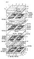
- Fig. 1 is a model view for illustrating one example of a method for manufacturing electronic components according to the present invention.
- Fig. 2a is a perspective view schematically showing one example of an electronic component according to the present invention.
- Fig. 2b is a schematic exploded view of the electronic component shown in Fig. 2a.
- Fig. 3a is a schematic cross-sectional view for illustrating an example of a laminate structure in a region in which removal dummy patterns and floating dummy patterns of a mother substrate are formed.
- Fig. 3b is a schematic cross-sectional view for illustrating an example of a laminate structure in a region in which removal dummy patterns and floating dummy patterns of a mother substrate are formed at positions different from those shown in Fig. 3a.
- Fig. 4 is a schematic cross-sectional view for illustrating another example.
- Fig. 5a is a model view showing an example of a coil component.
- Fig. 5b is a schematic cross-sectional view of the coil component shown in Fig. 5a taken along a line A-A.
- Fig. 6a is a view for illustrating an example of one manufacturing step of coil components.
- Fig. 6b is a view for illustrating an example of one step for manufacturing coil components, following the step shown in Fig. 6a.
- Fig. 7 is a model view for illustrating a problem of a conventional manufacturing process.
- Fig. 8 is a model view for illustrating an example of another manufacturing process of coil components.
- Fig. 9a is a model view for illustrating a problem of the example of the manufacturing process of coil components, which is illustrated with reference to Fig. 8.
- Fig. 9b is a model view for illustrating a problem of the manufacturing process of coil components, which is illustrated with reference to Fig. 8, together with Fig. 9a.
- Fig. 10 is a model view for illustrating another problem of the manufacturing process of coil components, which is illustrated with reference to Fig. 8.
-
- 1
- coil component
- 4, 5, 7, 8
- electronic component-forming conductive pattern
- 10, 11, 12, 13
- insulating layer
- 15
- floating dummy pattern
- 18
- removal dummy pattern
- Hereinafter, examples of the present invention will be described with reference to figures.
- In a schematic perspective view of Fig. 2a and a schematic exploded view of Fig. 2b, a coil component (common mode choke coil component) 1, which is an electronic component of this example, is shown. This
coil component 1 has the structure including a base-sidemagnetic substrate 2, an underlying insulatinglayer 3, a primary coil 6 made ofconductive patterns conductive patterns interlayer insulating layers layer 13, a lid-sidemagnetic substrate 14, floatingdummy patterns 15, and exterior connection electrodes 16 (16a, 16b) and 17 (17a, 17b). - The structure of this
coil component 1 will be described together with an example of its manufacturing process. In the manufacturing process of thecoil component 1 of this example, first of all, the base-sidemagnetic substrate 2 is prepared from which a plurality of thecoil components 1 as shown in Fig. 1 can be formed. Subsequently, the underlying insulatinglayer 3 is formed by lamination on the entire upper surface of the base-sidemagnetic substrate 2. As a substrate for forming the base-sidemagnetic substrate 2 and the lid-sidemagnetic substrate 14, for example, a ferrite substrate, a ceramic substrate containing a magnetic material, and a resin substrate containing a magnetic material may be mentioned. By using substrates appropriately selected from the substrates mentioned above, the base-sidemagnetic substrate 2 and the lid-sidemagnetic substrate 14 are formed. In addition, as an insulating material forming the individual insulating layers including the underlying insulatinglayer 3, the conductive pattern-interlayer insulating layers 10 to 12, and the protective insulatinglayer 13, for example, resin materials such as a polyimide resin, an epoxy resin, and a benzocyclobutene resin, photosensitive resin materials, glass materials such as SiO2, and glass ceramics may be mentioned. By using insulating materials appropriately selected from the insulating materials mentioned above, the individual insulating layers are formed. - Next, at the upper side of the underlying insulating
layer 3, the electronic component-formingconductive patterns 4 are formed by lamination in respective predetermined electronic component-forming regions R, and in addition, the floating dummy patterns 15 (15a) are also formed which are not electrically connected to the electronic component-formingconductive patterns 4. In addition, in a predetermined cutting-removal region Z which is to be removed by cutting in a cutting step to be described later, removal dummy patterns 18 (18a) are formed. In the example shown in Fig. 1, adjacent electronic component-formingconductive patterns 4 in the direction perpendicular to the plane of the figure are formed so that adjacent one-ends of theconductive patterns 4 extend and are then connected to each other. That is, an extension forming portion of theconductive patterns 4 is an extension conductor which is formed so as to extend from the electronic component-forming regions R and so as to intersect the cutting-removal region Z. - Incidentally, an allowable range is obtained beforehand and is determined in which, even when a cutting position is shifted in a cutting step which will be described later, the properties of the
coil component 1 are not seriously degraded by the shift of cutting position. In consideration of the shift of cutting position within the allowable range, the formation position and the width of the removal dummy pattern 18 (18a) are determined so as to be reliably cut and removed. In addition, in this example, the formation position of theremoval dummy pattern 18a is also determined in consideration of the following points. That is, also in the electronic component-formingconductive patterns conductive patterns 4, as is the case of theconductive patterns 4, adjacent electronic component-formingconductive patterns 7 in the direction perpendicular to the plane are formed so that adjacent one-ends of theconductive patterns 7 extend and are then connected to each other, and adjacent electronic component-formingconductive patterns 8 in the same direction as described above are formed so that adjacent one-ends of theconductive patterns 8 extend and are then connected to each other. A connection portion (extension conductor) X of theconductive patterns 7 and that of theconductive patterns 8 are each formed so as to extend from the electronic component-forming regions R and so as to intersect the cutting-removal region Z. In this example, theremoval dummy patterns 18a are formed at positions which are overlapped with those of the connection portions (extension conductors) X of the electronic component-formingconductive patterns - In this example, in consideration of the shift of cutting position in the cutting step within the allowable range, the floating dummy pattern 15 (15a) is provided at a position in the vicinity of the outside of the cutting-removal region Z at an interval therefrom so as not to be exposed at the side surface (cut surface) of the
electronic component 1 and is also provided adjacent to theremoval dummy pattern 18a at an interval therefrom. - As a method for forming a first conductive pattern layer including the electronic component-forming
conductive patterns 4, the floatingdummy patterns 15a, and theremoval dummy patterns 18a, various method may be mentioned, and any one of them may be used; however, as one example, a method using a photolithographic technique will be described. - When a photolithographic technique is used, for example, first of all, by using a film forming technique (such as a thin-film forming technique including sputtering or evaporation, or a thick-film forming technique including screen printing), a conductive material film for forming the
conductive patterns layer 3. As the conductive material, for example, a metal such as Ag, Pb, Cu, or Al, or an alloy thereof may be mentioned. In addition, it is preferable that a conductive material for forming the conductive patterns and an insulating material for forming the insulatinglayers - After the conductive material film is formed over the entire upper surface of the underlying insulating
layer 3, a resist film is formed on the entire surface of the conductive material film by application. Next, at the upper side of the resist film, a mask for forming theconductive patterns conductive patterns conductive patterns conductive patterns conductive patterns 4, the floatingdummy patterns 15a and theremoval dummy patterns 18a can be formed from the same material and in the same process, so that the first conductive pattern layer including theconductive patterns - At the upper side of the first conductive pattern layer, the conductive pattern-
interlayer insulating layer 10 is formed by lamination. In this conductive pattern-interlayer insulating layer 10, viaholes 20 are formed for connecting between the electronic component-formingconductive patterns layer 10 provided therebetween. In order to form the via holes 20, for example, the conductive pattern-interlayer insulating layer 10 can be formed using a photolithographic technique as described below. - For example, over the entire upper surface of the first conductive pattern layer, a photosensitive insulating material for forming the conductive pattern-
interlayer insulating layer 10 is formed by lamination. A mask for forming via holes is disposed at the upper side of this insulating material, and by using this mask, parts of the insulating material region except for places at which the via holes 20 are to be formed are irradiated with light such as ultraviolet rays for photo-curing. Subsequently, uncured parts of the insulating material are removed by development treatment. Accordingly, the via holes 20 are formed. As described above, the conductive pattern-interlayer insulating layer 10 provided with the via holes 20 can be formed. - At the upper side of the conductive pattern-
interlayer insulating layer 10, the electronic component-formingconductive patterns 5 are formed in the respective electronic component formation regions R by lamination, and in addition, the floating dummy patterns 15 (15b) are also formed which are not electrically connected to the electronic component-formingconductive patterns 5. In addition, in the cutting-removal region Z, the removal dummy patterns 18 (18b) are formed. - The electronic component-forming
conductive patterns 5 are formed so as to be approximately overlapped with the electronic component-formingconductive patterns 4 of the first conductive pattern layer. As is the case of theconductive patterns 4, adjacent electronic component-formingconductive patterns 5 in the direction perpendicular to the plane of Fig. 1 are formed so that adjacent one-ends of theconductive patterns 5 extend and are then connected to each other. The connection portion (extension conductor) X is provided so as to intersect the cutting-removal region Z, and the connection portion X is disposed at a position which is overlapped with that of the connection portion X of theconductive patterns 4 with the conductive pattern-interlayer insulating layer 10 provided therebetween. In addition, as is the case of the floatingdummy patterns 15a and theremoval dummy patterns 18a of the first conductive pattern layer, the formation position and the width of each of the floatingdummy patterns 15b and theremoval dummy patterns 18b are determined in consideration of the shift of cutting position. In this example, the floatingdummy patterns 15b and theremoval dummy patterns 18b are provided so as to be overlapped with the floatingdummy patterns 15a and theremoval dummy patterns 18a, respectively, with the conductive pattern-interlayer insulating layer 10 provided therebetween. - A second conductive pattern layer including the electronic component-forming
conductive patterns 5, the floatingdummy patterns 15b, and theremoval dummy patterns 18b as described above can be formed, for example, by using a photolithographic technique as is the case of the first conductive pattern layer. In addition, part of the conductive material forming theconductive patterns interlayer insulating layer 10. By the presence of the via holes 20, adjacentconductive patterns interlayer insulating layer 10 provided therebetween can be electrically connected to each other. - After the formation of the second conductive pattern layer, the conductive pattern-
interlayer insulating layer 11 is formed at the upper side of the second conductive pattern layer. At the upper side of the conductive pattern-interlayer insulating layer 11, the electronic component-formingconductive patterns 7 are formed by lamination in the respective electronic component-forming regions R, and in addition, the floating dummy patterns 15 (15c) are also formed which are not electrically connected to the electronic component-formingconductive patterns 7. In addition, in the cutting-removal region Z, the removal dummy patterns 18 (18c) are formed. - The electronic component-forming
conductive patterns 7 are formed so as to be overlapped with the positions at which the electronic component-formingconductive patterns conductive patterns conductive patterns 7 in the direction perpendicular to the plane of Fig. 1 are formed so that adjacent one-ends of theconductive patterns 7 extend and are then connected to each other. The connection portion (extension conductor) X is provided so as to intersect the cutting-removal region Z. However, the position at which the connection portion X is disposed is different from that of the connection portions X of theconductive patterns removal dummy patterns - As is the case of the
removal dummy patterns removal dummy pattern 18c is formed so as to have a size which can be placed within the cutting-removal region Z. Theremoval dummy pattern 18c is disposed at a position which is overlapped with that of the connection portions (extension conductors) X of theconductive patterns dummy patterns dummy pattern 15c is provided adjacent to theremoval dummy pattern 18c at an interval therefrom in consideration of the shift of cutting position and is disposed at a position which is overlapped with that of the connection portions X of theconductive patterns - A third conductive pattern layer including the electronic component-forming
conductive patterns 7, the floatingdummy patterns 15c, and theremoval dummy patterns 18c as described above can be formed using a photolithographic technique as is the case of the first and the second conductive pattern layers. At the upper side of the third conductive pattern layer, the conductive pattern-interlayer insulating layer 12 is formed by lamination. In this conductive pattern-interlayer insulating layer 12, viaholes 21 are formed for connecting between the electronic component-formingconductive patterns interlayer insulating layer 12 can also be formed using a photolithographic technique as is the conductive pattern-interlayer insulating layer 10. - At the upper side of the conductive pattern-
interlayer insulating layer 12, the electronic component-formingconductive patterns 8 are formed by lamination in the respective electronic component-forming regions R, and in addition, the floating dummy patterns 15 (15d) are also formed which are not electrically connected to the electronic component-formingconductive patterns 8. In addition, in the cutting-removal region Z, the removal dummy patterns 18 (18d) are formed. By theseconductive patterns 8, the floatingdummy patterns 15d, and theremoval dummy patterns 18d, a fourth conductive pattern layer is formed. - The electronic component-forming
conductive patterns 8 are formed so as to be approximately overlapped with the electronic component-formingconductive patterns conductive patterns 7, adjacent electronic component-formingconductive patterns 8 in the direction perpendicular to the plane of Fig. 1 are formed so that adjacent one-ends of theconductive patterns 8 extend and are then connected to each other. The connection portion (extension conductor) X is provided so as to intersect the cutting-removal region Z, and the connection portion (extension conductor) X is disposed at a position which is overlapped with that of the connection portion X of theconductive patterns 7. That is, in this example, as shown in a schematic cross-sectional view of Fig. 3a, theremoval dummy pattern 18a of the first conductive pattern layer, theremoval dummy pattern 18b of the second conductive pattern layer, the connection portion (extension conductor) X of theconductive patterns 7 of the third conductive pattern layer, and the connection portion (extension conductor) X of theconductive patterns 8 of the fourth conductive pattern layer are provided so as to be overlapped with each other. In other words, in the other conductive pattern layers (that is, the third and the fourth conductive pattern layers) in which the removal dummy patterns are not provided at positions which are overlapped with those of theremoval dummy patterns conductive patterns removal dummy patterns - As is the case of the
removal dummy patterns 18a to 18c, in consideration of the shift of cutting position within the allowable range, theremoval dummy pattern 18d is formed so as to have a size which can be placed within the cutting-removal region Z. Theremoval dummy pattern 18d is disposed at a position which is overlapped with that of theremoval dummy pattern 18c. That is, in this example, as shown in a schematic cross-sectional view of Fig. 3b, the connection portion X of theconductive patterns 4 of the first conductive pattern layer, the connection portion X of theconductive patterns 5 of the second conductive pattern layer, theremoval dummy pattern 18c of the third conductive pattern layer, and theremoval dummy pattern 18d of the fourth conductive pattern layer are provided so as to be overlapped with each other. In other words, in the other conductive pattern layers (that is, the first and the second conductive pattern layers) in which the removal dummy patterns are not provided at positions which are overlapped with those of theremoval dummy patterns conductive patterns removal dummy patterns - As is the case of the floating
dummy patterns 15a to 15c, the floatingdummy pattern 15d is provided adjacent to theremoval dummy pattern 18d at an interval therefrom in consideration of the shift of cutting position and is disposed so as to be overlapped with the floatingdummy pattern 15c of the third conductive pattern layer. In this example, when the cross section of the laminate along the line passing through the floatingdummy patterns dummy patterns 15 or the electronic component-forming conductive patterns are formed. - The fourth conductive pattern layer described above can also be formed by using a photolithographic technique as is the case of the first to the third conductive pattern layers. At the upper side of the fourth conductive pattern layer, the protective insulating
layer 13 is formed by lamination. - Subsequently, the lid-side
magnetic substrate 14 is disposed at the upper side of the protective insulatinglayer 13. In this step, an adhesive (such as thermosetting polyimide resin) is applied to a surface of the protective insulatinglayer 13 and a surface of the lid-sidemagnetic substrate 14, the surfaces facing each other. - Next, in a vacuum or an inert gas atmosphere, while being heated, the laminate including the
magnetic substrates layers magnetic substrate 14 and the protective insulatinglayer 13 are bonded to each other. Subsequently, after this laminate is cooled, the pressure applied thereto is released. As described above, a mother substrate is formed from which a great number of thecoil components 1 can be obtained by cutting. - After the mother substrate is formed, the laminate that was pressed previously is cut into individual
electronic components 1, for example, by dicing along the cutting lines set along the boundaries of the individual electronic component-forming regions R. At side surfaces (cut surfaces) of eachelectronic component 1 thus separated, end surfaces of the extension conductors of theconductive patterns - Subsequently, for each
electronic component 1, the exterior connection electrodes 16 (16a, 16b) and 17 (17a, 17b) are formed at respective positions at which the end surfaces of the extension conductors of theconductive patterns conductive patterns exterior connection electrode 16a and theexterior connection electrode 16b, respectively. Furthermore, one-end sides of theconductive patterns exterior connection electrode 17a and theexterior connection electrode 17b, respectively. - The
exterior connection electrodes - As described above, the
coil components 1 can be formed. In this example, since theremoval dummy patterns 18 and the floatingdummy patterns 15 are formed in regions of the conductive pattern layer other than those in which the electronic component-formingconductive patterns layer 13 is formed at the upper side of the fourth conductive pattern layer, the irregularities of the upper surface of the protective insulatinglayer 13 are reduced and planarized. Hence, when the lid-sidemagnetic substrate 14 is disposed at the upper side of the protective insulatinglayer 13, followed by application of a pressure, a pressing force can be approximately uniformly applied to the whole laminate. Accordingly, the generation of delamination caused by a non-uniformly applied pressing force can be suppressed. - In particular, in this example, the
removal dummy pattern 18 and the floatingdummy patterns 15 are disposed so as to be overlapped with the connection portion (extension conductor) X of the conductive patterns. In other words, at positions which are most responsible for forming theexterior connection electrodes 16 and 17 (that is, of regions in which delamination is liable to occur in the past, at positions at which a delamination problem most seriously occurs), theremoval dummy patterns 18 and the floatingdummy patterns 15 are disposed, so that the generation of delamination is prevented. - In addition, in this example, in consideration of the shift of cutting position, the
removal dummy pattern 18 is formed to have a small width so as to be placed within the cutting-removal region Z; however, since the floatingdummy pattern 15 is provided adjacent to the correspondingremoval dummy pattern 18 at an interval therefrom, even when theremoval dummy pattern 18 is formed to have a small width, the generation of a large gap between the patterns can be avoided which may cause a very large depression of the insulating layer. Accordingly, since the irregularities of the upper surface of the protective insulatinglayer 13 of the laminate can be reduced, the generation of delamination can be prevented as described above. - Furthermore, in this example, the floating
dummy patterns 15 and theremoval dummy patterns 18 are designed so that although the cutting position is shifted, when this shift is within an allowable range determined beforehand, the end surfaces of thedummy patterns coil component 1. Hence, the generation of problems such as migration between the dummy pattern and the electronic component-forming conductive pattern can be avoided. Accordingly, the degradation in electrical properties of the electronic component can be prevented, and hence a highly reliable electronic component having high performance can be easily provided. - Furthermore, in this example, the floating
dummy patterns 15 and theremoval dummy patterns 18 are formed along layer surfaces of the respective conductive pattern layer, and the floatingdummy patterns 15 and theremoval dummy patterns 18 are formed from the same material as that for forming the electronic component-formingconductive patterns - Furthermore, in this example, for example, in the third and fourth conductive pattern layers which do not have the removal dummy patterns at positions which are overlapped with those of the
removal dummy patterns 18a of the first conductive pattern layer, the extension conductors X of theconductive patterns removal dummy patterns 18a. As described above, in this example, in at least one of the other conductive pattern layers which do not have the removal dummy patterns at positions which are overlapped with the removal dummy patterns of one conductive pattern layer, the extension conductors of the electronic component-forming conductive patterns are formed at positions which are overlapped with the removal dummy patterns of said one conductive pattern layer. Accordingly, the irregularities of the upper surface of the laminate at places at which the extension conductors of the conductive patterns are formed can be reduced. - In addition, when a conductive pattern layer, which does not have floating dummy patterns at portions of the laminate at which floating dummy patterns are formed, is designed to have electronic component-forming conductive patterns so as to be overlapped with the above floating dummy patterns, in all the laminated conductive pattern layers in the floating dummy pattern-forming region, the floating dummy patterns or the electronic component-forming conductive patterns are formed so as to be overlapped with each other, and hence the irregularities of the upper surface of the laminate can be effectively reduced.
- In this example, the conductive pattern layers and the insulating layers are formed using a photolithographic technique. Hence, by highly precise machining using a photolithographic technique, the conductive pattern layers and the insulating layers can be formed substantially as designed. Accordingly, the variation in electrical properties of the electronic component can be suppressed, and more improvement in reliability of the electrical properties can be easily performed.
- The present invention is not limited to this example, and various embodiments may be performed. For example, in this example, as shown in a cross-sectional view of Fig. 3a, in all the second to the fourth conductive pattern layers, the floating
dummy patterns 15 or parts of the electronic component-formingconductive patterns dummy patterns 15a of the first conductive pattern layer. As described above, in this example, at the positions of all the other conductive pattern layers which are overlapped with the floating dummy patterns of one conductive pattern layer, respective floating dummy patterns or parts of the electronic component-forming conductive patterns are formed. On the other hand, for example, as shown by a schematic cross-sectional view of Fig. 4, of all the other conductive pattern layers which are overlapped with the floatingdummy patterns 15 of one conductive pattern layer, a conductive pattern layer may be present in which the floatingdummy patterns 15 and parts of the electronic component-forming conductive patterns are not formed at positions which are overlapped with those of the above floatingdummy patterns 15 of said one conductive pattern layer. In addition, the same situations can also be applied to theremoval dummy patterns 18, that is, of all the other conductive pattern layers which are overlapped with theremoval dummy patterns 18 of one conductive pattern layer, a conductive pattern layer may be present in which theremoval dummy patterns 18 and parts of the electronic component-forming conductive patterns are not formed at positions which are overlapped with those of the aboveremoval dummy patterns 18 of said one conductive pattern layer. - In addition, in this example, the floating
dummy patterns 15 and theremoval dummy patterns 18 are disposed at positions which are overlapped with those of the connection portions (extension conductors) X of the electronic component-forming conductive patterns; however, the floatingdummy patterns 15 and theremoval dummy patterns 18 may be disposed at positions which are not overlapped with those of the electronic component-forming conductive patterns. In this case, for example, in the cutting-removal region Z, theremoval dummy patterns 18 may be formed in all the first to the fourth conductive pattern layers or may be formed only in three conductive pattern layers or less which are selected beforehand from the first to the fourth conductive pattern layers. As is the case described above, when the floatingdummy patterns 15 are provided at positions which are not overlapped with those of the electronic component-forming conductive patterns, the floatingdummy patterns 15 may be formed in all the first to the fourth conductive pattern layers or may be formed only in three conductive pattern layers or less which are selected beforehand from the first to the fourth conductive pattern layers. - Furthermore, in this example, although the
coil component 1 uses a magnetic substrate, instead of the magnetic substrate, for example, a dielectric substrate may be provided. As an insulating material forming this dielectric substrate, for example, a resin material such as a polyimide resin, an epoxy resin, or a benzocyclobutene resin, a photosensitive resin material, a glass material such SiO2, and a dielectric ceramic such as a glass ceramic or BaTiO3 may be mentioned. In addition, in this example, although the substrates are provided on both side of the laminate, which is formed by alternately laminating the conductive pattern layers and the insulating layers, in the up and down direction, for example, instead of at least one substrate provided on the top or the bottom side, a protective layer may be provided which is formed by applying a molten insulating material, followed by curing. As described above, on both sides of the laminate in the up and down direction, the substrates are not always necessarily provided. - Furthermore, in this example, the present invention is described with reference to the coil component (common mode choke coil component) by way of example; however, when the structure is used in which conductive pattern layers are laminated to each other with at least one insulating layer provided therebetween, the present invention may be applied to an electronic component besides a common mode choke coil component, to a method for manufacturing the electronic component, and to a mother substrate for forming many electronic components.
- By forming the structure according to the present invention, a compact and high-performance electronic component can be provided, and hence the present invention is effectively applied to an electronic component to be incorporated in a device which is required to reduce its size, to a method for manufacturing electronic components, and to a mother substrate for forming many electronic components.
Claims (17)
- A method for manufacturing electronic components, in which conductive pattern layers are laminated to each other with insulating layers provided therebetween to form an integrated laminate, comprising the steps of:alternately laminating the insulating layers and conductive pattern layers having conductive patterns which are formed at intervals therebetween in layer surface directions to form a laminate in which laminate portions of electronic component-forming conductive patterns are collectively formed;after a force is applied to the laminate in the lamination direction to form the integrated laminate, cutting the laminate along cutting lines provided along boundaries of the laminate portions of the electronic component-forming conductive patterns so as to separate the electronic components from each other;forming at least one removal dummy pattern in at least one of the conductive pattern layers which are to be laminated to each other before an insulating layer is provided on a surface of said at least one of the conductive pattern layers, the removal dummy pattern having a size to be placed within a cutting-removal region which is a region to be cut and removed by the step of cutting the laminate; andforming at least one floating dummy pattern in at least one conductive pattern layer of the laminate portions of the electronic component-forming conductive patterns so as to be disposed in the vicinity of the outside of the cutting-removal region at an interval therefrom before an insulating layer is formed by lamination on a surface of said at least one conductive pattern layer, the floating dummy pattern being not electrically connected to the electronic component-forming conductive patterns.
- The method for manufacturing electronic components, according to Claim 1, wherein at least one floating dummy pattern and at least one removal dummy pattern are disposed in at least one of the conductive pattern layers so as to be adjacent to each other at an interval therebetween in a layer surface direction of said at least one of the conductive pattern layers, and electronic component-forming conductive patterns of said at least one of the conductive pattern layers, said at least one floating dummy pattern, and said at least one removal dummy pattern are formed from the same material and are also formed in the same step.
- The method for manufacturing electronic components, according to Claim 1, wherein one conductive pattern layer is disposed which does not have at least one removal dummy pattern at a position which is overlapped with that of at least one removal dummy pattern of another conductive pattern layer, at least one extension conductor is extendedly formed in said one conductive pattern layer from electronic component-forming conductive patterns thereof so as to intersect the cutting-removal region, and said at least one removal dummy pattern of said another conductive pattern layer and said at least one extension conductor of said one conductive pattern layer are provided at positions which are overlapped with each other.
- The method for manufacturing electronic components, according to Claim 1, wherein conductive patterns of one conductive pattern layer are disposed, said one conductive pattern layer having no floating dummy pattern at a position which is overlapped with that of at least one floating dummy pattern of another conductive pattern layer, and the floating dummy pattern of said another conductive pattern layer and part of the conductive patterns of said one conductive pattern layer are provided at positions which are overlapped with each other.
- The method for manufacturing electronic components, according to Claim 3, wherein conductive patterns of one conductive pattern layer are disposed, said one conductive pattern layer having no floating dummy pattern at a position which is overlapped with that of at least one floating dummy pattern of another conductive pattern layer, and the floating dummy pattern of said another conductive pattern layer and part of the conductive patterns of said one conductive pattern layer are provided at positions which are overlapped with each other.
- The method for manufacturing electronic components, according to Claim 1, wherein the conductive pattern layers and the insulating layers are formed using a photolithographic technique.
- The method for manufacturing electronic components, according to one of Claims 1 to 6, wherein the electronic component-forming conductive patterns have a coil pattern shape, and the electronic components are coil components.
- A mother substrate for forming many electronic components, comprising: conductive pattern layers having conductive patterns which are formed at intervals therebetween in layer surface directions; and insulating layers which are alternately laminated with the conductive pattern layers to form a laminate in which laminate portions of electronic component-forming conductive patterns are collectively formed, the laminate being cut along cutting lines provided along boundaries of the laminate portions of the electronic component-forming conductive patterns so as to separate the electronic components from each other,
wherein in at least one of the conductive pattern layers which are to be laminated to each other, at least one removal dummy pattern is formed having a size to be placed within a cutting-removal region which is to be cut away along the cutting lines, and
in at least one conductive pattern layer of the laminate portions of the electronic component-forming conductive patterns, at least one floating dummy pattern which is not electrically connected to the electronic component-forming conductive patterns is formed in the vicinity of the outside of the cutting-removal region at an interval therefrom. - The mother substrate for forming many electronic components, according to Claim 8, wherein at least one floating dummy pattern and at least one removal dummy pattern are disposed in at least one of the conductive pattern layers so as to be adjacent to each other at an interval therebetween, and electronic component-forming conductive patterns of said at least one of the conductive pattern layers, said at least one floating dummy pattern, and said at least one removal dummy pattern are formed from the same material.
- The mother substrate for forming many electronic components, according to Claim 8, wherein in at least one of other conductive pattern layers having no removal dummy pattern at a position which is overlapped with at least one removal dummy pattern of one conductive pattern layer, at least one extension conductor is extendedly formed from electronic component-forming conductive patterns of said at least one of other conductive pattern layers to intersect the cutting-removal region, and said at least one removal dummy pattern of said one conductive pattern layer and said at least one extension conductor of said at least one of other conductive pattern layers are provided at positions which are overlapped with each other.
- The mother substrate for forming many electronic components, according to Claim 8, wherein in at least one of other conductive pattern layers having no floating dummy pattern at a position which is overlapped with at least one floating dummy pattern of one conductive pattern layer, part of electronic component-forming conductive patterns of said at least one of other conductive pattern layers is disposed at a position which is overlapped with that of said at least one floating dummy pattern of said one conductive pattern layer.
- The mother substrate for forming many electronic components, according to Claim 10, wherein in at least one of other conductive pattern layers having no floating dummy pattern at a position which is overlapped with at least one floating dummy pattern of one conductive pattern layer, part of electronic component-forming conductive patterns of said at least one of other conductive pattern layers is disposed at a position which is overlapped with that of said at least one floating dummy pattern of said one conductive pattern layer.
- The mother substrate for forming many electronic components, according to Claim 8, wherein the conductive pattern layers and the insulating layers are formed using a photolithographic technique.
- The mother substrate for forming many electronic components, according to one of Claims 8 to 13, wherein the electronic component-forming conductive patterns have a coil pattern shape, and the electronic components are coil components.
- An electronic component comprising: conductive pattern layers; and insulating layers which are alternately laminated with the conductive pattern layers to form a laminate in which the conductive pattern layers are integrally laminated to each other,
wherein in at least one of the conductive pattern layers which are laminated to each other, at least one floating dummy pattern which is not electrically connected to a corresponding conductive pattern is disposed in a region between an end surface of said at least one of the conductive pattern layers and the conductive pattern at an interval therefrom so as not to be exposed at the end surface of said at least one of the conductive pattern layers. - The electronic component according to Claim 15,
wherein the conductive pattern layers have extension conductors which are extendedly formed from the conductive patterns so as to extend to end surfaces of the conductive pattern layers, conductive pattern layers having extension conductors formed at positions different from each other are included in the conductive pattern layers which are laminated to each other, and of the conductive pattern layers having extension conductors formed at positions different from each other, in a region of one conductive pattern layer in which no floating dummy pattern is formed and which is overlapped with a region of another conductive pattern layer in which at least one extension conductor is formed, at least one floating dummy pattern is formed. - The electronic component according to Claim 15 or 16,
wherein the electronic component-forming conductive patterns have a coil pattern shape, and the electronic component is a coil component.
Applications Claiming Priority (2)
| Application Number | Priority Date | Filing Date | Title |
|---|---|---|---|
| JP2004216029 | 2004-07-23 | ||
| PCT/JP2005/009779 WO2006011291A1 (en) | 2004-07-23 | 2005-05-27 | Method for manufacturing electronic component, parent board and electronic component |
Publications (2)
| Publication Number | Publication Date |
|---|---|
| EP1772878A1 true EP1772878A1 (en) | 2007-04-11 |
| EP1772878A4 EP1772878A4 (en) | 2012-12-12 |
Family
ID=35786046
Family Applications (1)
| Application Number | Title | Priority Date | Filing Date |
|---|---|---|---|
| EP05743677A Withdrawn EP1772878A4 (en) | 2004-07-23 | 2005-05-27 | METHOD FOR PRODUCING AN ELECTRONIC COMPONENT, NUT PLATE AND ELECTRONIC COMPONENT |
Country Status (6)
| Country | Link |
|---|---|
| US (1) | US7663225B2 (en) |
| EP (1) | EP1772878A4 (en) |
| JP (2) | JP4225349B2 (en) |
| CN (1) | CN1914699B (en) |
| TW (1) | TWI271751B (en) |
| WO (1) | WO2006011291A1 (en) |
Families Citing this family (33)
| Publication number | Priority date | Publication date | Assignee | Title |
|---|---|---|---|---|
| JP4225349B2 (en) * | 2004-07-23 | 2009-02-18 | 株式会社村田製作所 | Manufacturing method of electronic component, parent substrate and electronic component |
| JP4844045B2 (en) * | 2005-08-18 | 2011-12-21 | Tdk株式会社 | Electronic component and manufacturing method thereof |
| US20100193122A1 (en) * | 2007-06-19 | 2010-08-05 | Sumitomo Bakelite Co., Ltd. | Process for manufacturing electronic device |
| JP5338663B2 (en) * | 2007-06-19 | 2013-11-13 | 住友ベークライト株式会社 | Manufacturing method of electronic device |
| TW201106386A (en) * | 2009-08-03 | 2011-02-16 | Inpaq Technology Co Ltd | Common mode filter and method of manufacturing the same |
| KR101133397B1 (en) * | 2010-04-05 | 2012-04-09 | 삼성전기주식회사 | Planar transformer and manufacturing method thereof |
| US8451083B2 (en) * | 2010-05-31 | 2013-05-28 | Tdk Corporation | Coil component and method of manufacturing the same |
| JP5595813B2 (en) * | 2010-07-09 | 2014-09-24 | 株式会社東海理化電機製作所 | Circuit board manufacturing method |
| ITTO20110295A1 (en) * | 2011-04-01 | 2012-10-02 | St Microelectronics Srl | INDUCTOR INTEGRATED DEVICE WITH HIGH INDUCTANCE VALUE, IN PARTICULAR FOR USE AS AN ANTENNA IN A RADIOFREQUENCY IDENTIFICATION SYSTEM |
| WO2013065716A1 (en) * | 2011-11-04 | 2013-05-10 | 株式会社村田製作所 | Common mode choke coil and high-frequency electronic device |
| WO2013099540A1 (en) * | 2011-12-27 | 2013-07-04 | 株式会社村田製作所 | Laminated common-mode choke coil |
| KR20130077400A (en) * | 2011-12-29 | 2013-07-09 | 삼성전기주식회사 | Thin film type coil component and fabricating method thereof |
| WO2013128702A1 (en) * | 2012-02-29 | 2013-09-06 | 株式会社村田製作所 | Laminated inductor and power supply circuit module |
| US9000876B2 (en) * | 2012-03-13 | 2015-04-07 | Taiwan Semiconductor Manufacturing Company, Ltd. | Inductor for post passivation interconnect |
| KR101397488B1 (en) * | 2012-07-04 | 2014-05-20 | 티디케이가부시기가이샤 | Coil component and method of manufacturing the same |
| KR101771729B1 (en) * | 2012-07-25 | 2017-08-25 | 삼성전기주식회사 | Multilayer inductor and protective composition for multilayer inductor |
| US8633793B1 (en) * | 2012-10-05 | 2014-01-21 | Inpaq Technology Co., Ltd. | Common mode filter |
| JP5978915B2 (en) * | 2012-10-19 | 2016-08-24 | 株式会社村田製作所 | Multilayer inductor |
| JP5958377B2 (en) * | 2013-02-14 | 2016-07-27 | 株式会社村田製作所 | Trance |
| KR20150062556A (en) * | 2013-11-29 | 2015-06-08 | 삼성전기주식회사 | Strip level substrate having a member of preventing warpage and method of manufacturing the same |
| US10083486B2 (en) * | 2013-12-31 | 2018-09-25 | Nyse Group, Inc. | Limited movement collar on marketable order execution price |
| JP6070900B2 (en) * | 2014-05-15 | 2017-02-01 | 株式会社村田製作所 | Multilayer coil component and manufacturing method thereof |
| JP6500635B2 (en) * | 2015-06-24 | 2019-04-17 | 株式会社村田製作所 | Method of manufacturing coil component and coil component |
| US9646758B2 (en) * | 2015-07-14 | 2017-05-09 | Globalfoundries Inc. | Method of fabricating integrated circuit (IC) devices |
| JP6536437B2 (en) * | 2016-03-04 | 2019-07-03 | 株式会社村田製作所 | Electronic parts |
| CN209731748U (en) * | 2016-06-22 | 2019-12-03 | 株式会社村田制作所 | Multilayer substrate |
| JP6919194B2 (en) * | 2016-12-27 | 2021-08-18 | Tdk株式会社 | Coil parts and circuit boards equipped with them |
| JP6828555B2 (en) | 2017-03-29 | 2021-02-10 | Tdk株式会社 | Coil parts and their manufacturing methods |
| WO2018225445A1 (en) * | 2017-06-05 | 2018-12-13 | 株式会社村田製作所 | Ceramic substrate with built-in coil |
| JP6696483B2 (en) * | 2017-07-10 | 2020-05-20 | 株式会社村田製作所 | Coil parts |
| JP6819499B2 (en) * | 2017-07-25 | 2021-01-27 | 株式会社村田製作所 | Coil parts and their manufacturing methods |
| WO2020121801A1 (en) * | 2018-12-11 | 2020-06-18 | 株式会社村田製作所 | Resin multilayer substrate and method for producing resin multilayer substrate |
| JP7435351B2 (en) * | 2020-08-05 | 2024-02-21 | 株式会社村田製作所 | common mode choke coil |
Family Cites Families (14)
| Publication number | Priority date | Publication date | Assignee | Title |
|---|---|---|---|---|
| JP3320096B2 (en) * | 1992-05-07 | 2002-09-03 | ティーディーケイ株式会社 | Multilayer inductor and method of manufacturing the same |
| JP3150022B2 (en) * | 1993-10-27 | 2001-03-26 | 横河電機株式会社 | Laminated print coil and method of manufacturing the same |
| JPH0982558A (en) * | 1995-09-18 | 1997-03-28 | Murata Mfg Co Ltd | Multilayer ceramic electronic component |
| US6356181B1 (en) * | 1996-03-29 | 2002-03-12 | Murata Manufacturing Co., Ltd. | Laminated common-mode choke coil |
| JPH09289128A (en) * | 1996-04-19 | 1997-11-04 | Matsushita Electric Works Ltd | Manufacture of multilayer board for printed coil |
| JP3615024B2 (en) * | 1997-08-04 | 2005-01-26 | 株式会社村田製作所 | Coil parts |
| JP3011174B2 (en) | 1998-02-26 | 2000-02-21 | 株式会社村田製作所 | Direction recognition method for thin-film coil components |
| JP2000012377A (en) * | 1998-06-17 | 2000-01-14 | Murata Mfg Co Ltd | Laminated ceramic electronic component and manufacture of the same |
| JP2001217139A (en) * | 2000-01-31 | 2001-08-10 | Kyocera Corp | Manufacturing method of laminated electronic components |
| JP2003158376A (en) | 2002-09-02 | 2003-05-30 | Ibiden Co Ltd | Method for manufacturing ceramic multi-layer substrate |
| JP3881949B2 (en) | 2002-10-17 | 2007-02-14 | 東洋アルミニウム株式会社 | ANTENNA CIRCUIT COMPOSITION, FUNCTIONAL CARD HAVING THE SAME, AND METHOD FOR MANUFACTURING ANTENNA CIRCUIT COMPOSITION |
| JP2004186343A (en) * | 2002-12-02 | 2004-07-02 | Kyocera Corp | Ceramic laminate and manufacturing method thereof |
| JP4225349B2 (en) * | 2004-07-23 | 2009-02-18 | 株式会社村田製作所 | Manufacturing method of electronic component, parent substrate and electronic component |
| JP4622367B2 (en) * | 2004-07-27 | 2011-02-02 | 株式会社村田製作所 | Electronic components |
-
2005
- 2005-05-27 JP JP2006528418A patent/JP4225349B2/en not_active Expired - Fee Related
- 2005-05-27 EP EP05743677A patent/EP1772878A4/en not_active Withdrawn
- 2005-05-27 CN CN2005800037683A patent/CN1914699B/en not_active Expired - Fee Related
- 2005-05-27 US US10/599,368 patent/US7663225B2/en not_active Expired - Fee Related
- 2005-05-27 WO PCT/JP2005/009779 patent/WO2006011291A1/en not_active Ceased
- 2005-06-09 TW TW094118978A patent/TWI271751B/en not_active IP Right Cessation
-
2008
- 2008-10-06 JP JP2008260165A patent/JP4636160B2/en not_active Expired - Fee Related
Also Published As
| Publication number | Publication date |
|---|---|
| JP4225349B2 (en) | 2009-02-18 |
| CN1914699B (en) | 2011-07-13 |
| TW200605105A (en) | 2006-02-01 |
| CN1914699A (en) | 2007-02-14 |
| JP4636160B2 (en) | 2011-02-23 |
| US20070199734A1 (en) | 2007-08-30 |
| US7663225B2 (en) | 2010-02-16 |
| JPWO2006011291A1 (en) | 2008-05-01 |
| TWI271751B (en) | 2007-01-21 |
| JP2009044175A (en) | 2009-02-26 |
| EP1772878A4 (en) | 2012-12-12 |
| WO2006011291A1 (en) | 2006-02-02 |
Similar Documents
| Publication | Publication Date | Title |
|---|---|---|
| EP1772878A1 (en) | Method for manufacturing electronic component, parent board and electronic component | |
| JP6665838B2 (en) | Inductor components | |
| CN112951541B (en) | Electronic component | |
| US7791445B2 (en) | Low profile layered coil and cores for magnetic components | |
| US7935891B2 (en) | Wiring board manufacturing method | |
| CN108288534B (en) | Inductance component | |
| US10886057B2 (en) | Electronic component | |
| KR20010032411A (en) | Improved miniature surface mount capacitor and method of making same | |
| JPS6317359B2 (en) | ||
| JPH04355933A (en) | Packaging structure of flip chip | |
| CN102349359A (en) | Resin wiring board | |
| CN219204859U (en) | Multilayer substrate | |
| US8426249B2 (en) | Chip part manufacturing method and chip parts | |
| KR102545033B1 (en) | Coil Electronic Component | |
| EP0147566B1 (en) | Method of forming contacts for flexible module carriers | |
| US8378225B2 (en) | Printed circuit board and method for fabricating the same | |
| JP2006173163A (en) | Chip coil | |
| EP0836228A2 (en) | Improvements in or relating to carrier tapes | |
| JP7347037B2 (en) | Manufacturing method of electronic components | |
| JPH06350230A (en) | Printed wiring board and production thereof | |
| KR100809529B1 (en) | Method of manufacturing electronic components, parent substrates and electronic components | |
| US20240186056A1 (en) | Coil component and manufacturing method therefor | |
| JPH08288102A (en) | Electronic component and its manufacture | |
| WO2004093105A1 (en) | Method of forming sheet having foreign material portions used for forming multilayer wiring board and sheet having foreign portions | |
| CN119480368A (en) | Electronic component and method for manufacturing the same |
Legal Events
| Date | Code | Title | Description |
|---|---|---|---|
| PUAI | Public reference made under article 153(3) epc to a published international application that has entered the european phase |
Free format text: ORIGINAL CODE: 0009012 |
|
| 17P | Request for examination filed |
Effective date: 20060929 |
|
| AK | Designated contracting states |
Kind code of ref document: A1 Designated state(s): AT BE BG CH CY CZ DE DK EE ES FI FR GB GR HU IE IS IT LI LT LU MC NL PL PT RO SE SI SK TR |
|
| DAX | Request for extension of the european patent (deleted) | ||
| A4 | Supplementary search report drawn up and despatched |
Effective date: 20121109 |
|
| RIC1 | Information provided on ipc code assigned before grant |
Ipc: H01F 17/00 20060101ALI20121105BHEP Ipc: H01G 4/012 20060101ALI20121105BHEP Ipc: H01G 4/30 20060101ALI20121105BHEP Ipc: H05K 3/00 20060101ALI20121105BHEP Ipc: H01G 4/12 20060101ALI20121105BHEP Ipc: H01F 41/04 20060101AFI20121105BHEP |
|
| STAA | Information on the status of an ep patent application or granted ep patent |
Free format text: STATUS: THE APPLICATION HAS BEEN WITHDRAWN |
|
| 18W | Application withdrawn |
Effective date: 20130226 |