EP1768215A2 - Plasma Display Device - Google Patents
Plasma Display Device Download PDFInfo
- Publication number
- EP1768215A2 EP1768215A2 EP06121218A EP06121218A EP1768215A2 EP 1768215 A2 EP1768215 A2 EP 1768215A2 EP 06121218 A EP06121218 A EP 06121218A EP 06121218 A EP06121218 A EP 06121218A EP 1768215 A2 EP1768215 A2 EP 1768215A2
- Authority
- EP
- European Patent Office
- Prior art keywords
- plasma display
- display device
- display panel
- anisotropic conductive
- particles
- Prior art date
- Legal status (The legal status is an assumption and is not a legal conclusion. Google has not performed a legal analysis and makes no representation as to the accuracy of the status listed.)
- Withdrawn
Links
Images




Classifications
-
- H—ELECTRICITY
- H05—ELECTRIC TECHNIQUES NOT OTHERWISE PROVIDED FOR
- H05K—PRINTED CIRCUITS; CASINGS OR CONSTRUCTIONAL DETAILS OF ELECTRIC APPARATUS; MANUFACTURE OF ASSEMBLAGES OF ELECTRICAL COMPONENTS
- H05K3/00—Apparatus or processes for manufacturing printed circuits
- H05K3/30—Assembling printed circuits with electric components, e.g. with resistors
- H05K3/32—Assembling printed circuits with electric components, e.g. with resistors electrically connecting electric components or wires to printed circuits
- H05K3/321—Assembling printed circuits with electric components, e.g. with resistors electrically connecting electric components or wires to printed circuits by conductive adhesives
- H05K3/323—Assembling printed circuits with electric components, e.g. with resistors electrically connecting electric components or wires to printed circuits by conductive adhesives by applying an anisotropic conductive adhesive layer over an array of pads
-
- H—ELECTRICITY
- H01—ELECTRIC ELEMENTS
- H01R—ELECTRICALLY-CONDUCTIVE CONNECTIONS; STRUCTURAL ASSOCIATIONS OF A PLURALITY OF MUTUALLY-INSULATED ELECTRICAL CONNECTING ELEMENTS; COUPLING DEVICES; CURRENT COLLECTORS
- H01R12/00—Structural associations of a plurality of mutually-insulated electrical connecting elements, specially adapted for printed circuits, e.g. printed circuit boards [PCB], flat or ribbon cables, or like generally planar structures, e.g. terminal strips, terminal blocks; Coupling devices specially adapted for printed circuits, flat or ribbon cables, or like generally planar structures; Terminals specially adapted for contact with, or insertion into, printed circuits, flat or ribbon cables, or like generally planar structures
- H01R12/50—Fixed connections
- H01R12/59—Fixed connections for flexible printed circuits, flat or ribbon cables or like structures
- H01R12/62—Fixed connections for flexible printed circuits, flat or ribbon cables or like structures connecting to rigid printed circuits or like structures
-
- H—ELECTRICITY
- H01—ELECTRIC ELEMENTS
- H01J—ELECTRIC DISCHARGE TUBES OR DISCHARGE LAMPS
- H01J2211/00—Plasma display panels with alternate current induction of the discharge, e.g. AC-PDPs
- H01J2211/20—Constructional details
- H01J2211/46—Connecting or feeding means, e.g. leading-in conductors
-
- H—ELECTRICITY
- H01—ELECTRIC ELEMENTS
- H01R—ELECTRICALLY-CONDUCTIVE CONNECTIONS; STRUCTURAL ASSOCIATIONS OF A PLURALITY OF MUTUALLY-INSULATED ELECTRICAL CONNECTING ELEMENTS; COUPLING DEVICES; CURRENT COLLECTORS
- H01R4/00—Electrically-conductive connections between two or more conductive members in direct contact, i.e. touching one another; Means for effecting or maintaining such contact; Electrically-conductive connections having two or more spaced connecting locations for conductors and using contact members penetrating insulation
- H01R4/04—Electrically-conductive connections between two or more conductive members in direct contact, i.e. touching one another; Means for effecting or maintaining such contact; Electrically-conductive connections having two or more spaced connecting locations for conductors and using contact members penetrating insulation using electrically conductive adhesives
-
- H—ELECTRICITY
- H05—ELECTRIC TECHNIQUES NOT OTHERWISE PROVIDED FOR
- H05K—PRINTED CIRCUITS; CASINGS OR CONSTRUCTIONAL DETAILS OF ELECTRIC APPARATUS; MANUFACTURE OF ASSEMBLAGES OF ELECTRICAL COMPONENTS
- H05K2201/00—Indexing scheme relating to printed circuits covered by H05K1/00
- H05K2201/09—Shape and layout
- H05K2201/09818—Shape or layout details not covered by a single group of H05K2201/09009 - H05K2201/09809
- H05K2201/09881—Coating only between conductors, i.e. flush with the conductors
-
- H—ELECTRICITY
- H05—ELECTRIC TECHNIQUES NOT OTHERWISE PROVIDED FOR
- H05K—PRINTED CIRCUITS; CASINGS OR CONSTRUCTIONAL DETAILS OF ELECTRIC APPARATUS; MANUFACTURE OF ASSEMBLAGES OF ELECTRICAL COMPONENTS
- H05K2201/00—Indexing scheme relating to printed circuits covered by H05K1/00
- H05K2201/10—Details of components or other objects attached to or integrated in a printed circuit board
- H05K2201/10613—Details of electrical connections of non-printed components, e.g. special leads
- H05K2201/10621—Components characterised by their electrical contacts
- H05K2201/10681—Tape Carrier Package [TCP]; Flexible sheet connector
-
- H—ELECTRICITY
- H05—ELECTRIC TECHNIQUES NOT OTHERWISE PROVIDED FOR
- H05K—PRINTED CIRCUITS; CASINGS OR CONSTRUCTIONAL DETAILS OF ELECTRIC APPARATUS; MANUFACTURE OF ASSEMBLAGES OF ELECTRICAL COMPONENTS
- H05K2203/00—Indexing scheme relating to apparatus or processes for manufacturing printed circuits covered by H05K3/00
- H05K2203/11—Treatments characterised by their effect, e.g. heating, cooling, roughening
- H05K2203/1189—Pressing leads, bumps or a die through an insulating layer
-
- H—ELECTRICITY
- H05—ELECTRIC TECHNIQUES NOT OTHERWISE PROVIDED FOR
- H05K—PRINTED CIRCUITS; CASINGS OR CONSTRUCTIONAL DETAILS OF ELECTRIC APPARATUS; MANUFACTURE OF ASSEMBLAGES OF ELECTRICAL COMPONENTS
- H05K3/00—Apparatus or processes for manufacturing printed circuits
- H05K3/30—Assembling printed circuits with electric components, e.g. with resistors
- H05K3/303—Assembling printed circuits with electric components, e.g. with resistors with surface mounted components
- H05K3/305—Affixing by adhesive
-
- H—ELECTRICITY
- H05—ELECTRIC TECHNIQUES NOT OTHERWISE PROVIDED FOR
- H05K—PRINTED CIRCUITS; CASINGS OR CONSTRUCTIONAL DETAILS OF ELECTRIC APPARATUS; MANUFACTURE OF ASSEMBLAGES OF ELECTRICAL COMPONENTS
- H05K3/00—Apparatus or processes for manufacturing printed circuits
- H05K3/36—Assembling printed circuits with other printed circuits
- H05K3/361—Assembling flexible printed circuits with other printed circuits
Definitions
- the present invention relates to a plasma display device. More particularly, the present invention relates to a plasma display device in which a connecting member is improved to have a high adhesive insulating property.
- a plasma display panel is a device using a plasma discharging structure to display an image.
- Such a plasma display device includes an electrode (for example, an address electrode) which is electrically connected to a driving circuit via a flexible printed circuit (FPC).
- the FPC includes a driver integrated circuit (IC) which applies voltages depending on the signal controlled by the driving circuit to selectively provide the wall voltage to the region corresponding to pixels of the plasma display panel.
- IC driver integrated circuit
- a chip on film has generally been used to applying the voltage using the FPC and the driver IC.
- COF chip on film
- TCP tape carrier package
- the FPC or the TCP is electrically connected to the metal electrode terminal using an anisotropic conductive film (ACF).
- ACF anisotropic conductive film
- the anisotropic conductive film is generally a resin film made conductive by the inclusion of conductive metal particles.
- connection structure of a prior art anisotropic conductive film is described in more detailed.
- an electrode terminal 32 of the plasma display panel 30 is attached with the anisotropic conductive film 34.
- the FPC terminal is introduced thereon, and the electrode of the plasma display panel and the terminal of the FPC are compressed to electrically connect the ball-type conductive metal particles dispersed in the conductive resin of the plasma display panel to the electrode of the plasma display panel and to the terminal of the FPC.
- the anisotropic conductive film is attached by applying the anisotropic conductive film to the electrode terminal with the exception of the portion of the electrode terminal that connects with the plasma display panel and the portion of the electrode terminal to be connected with the FPC.
- the initial portion and the end portion of the terminal are not covered with the anisotropic conductive film. This prevents the aggregation of the conductive metal particles from the anisotropic conductive film on those portions of the electrode terminal when the anisotropic conductive film is expanded during the compressing process, preventing an electrical connection between the electrode of the plasma display panel and the terminal of the FPC in order to prevent a potential short circuit.
- the conductive resin of the anisotropic conductive film still flows out during the compression process and the conductive metal particles tend to aggregate at the initial and end portions of the electrode terminal which can result in a short circuit. Further, an excess of the conductive metal particles tend to aggregate at the gap portion instead of the electrode portion during the compression process. In general, about 30% of the conductive metal particles are present at the electrode with about 70% at the gap away from the electrode. As a result, electron movement is not facilitated between terminals due to the use of the conductive metal particles.
- the address electrode is mainly coated with silver. This can lead to a short circuit since air pockets, voids, and pores are generated due to impurities between the terminals, the low adhesive strength of the anisotropic conductive film, and since the micropores are generated in the anisotropic polymer of the anisotropic conductive film during the compression process.
- the problems also include migration that occurs due to the adhesive reinforcement of the electrode.
- the plasma display device includes a plasma display panel, a driving circuit for driving the plasma display panel, an electrical signal transmitting wire electrically connecting an electrode extended from the plasma display panel to the driving circuit, and an adhesive film interposed between the terminal of the electrical signal transmitting wire and the terminal of the electrode of the plasma display panel and connecting both terminals.
- the adhesive film includes an anisotropic conductive film including conductive particles.
- the adhesive film includes an anisotropic conductive film including conductive particles and at least one insulated section referred to as a "dummy" the dummy being located either at the end of the anisotropic conductive film toward the plasma display panel, at the opposite end, or at both ends.
- the adhesive film includes an anisotropic conductive comprising a plurality of conductive particles with insulated layers positioned on either side to form the anisotropic conductive film layer.
- the present invention relates to an adhesive film such as an anisotropic conductive film (ACF) connecting a metal bus electrode and an address electrode to an electrical signal transmitting wire such as FPC or TCP.
- the electrode is connected to the electrical signal transmitting wire using conductive particles provided in an adhesive film, but the conductive particles do not aggregate, and do not migrate by an excessive amount away from the electrode. This helps to prevent formation of an abnormal conductive path in order to facilitate electron transmission while preventing a short circuit.
- the plasma display device includes a plasma display panel, a driving circuit for driving the plasma display panel, an electrical signal transmitting wire electrically connecting the electrode and extending from the plasma display panel to the driving circuit, and an adhesive film interposed between the terminal of the electrical signal wire and the terminal of the electrode of the plasma display panel, electrically connecting the terminals.
- the adhesive film includes an anisotropic conductive film including conductive particles with an insulated dummy at least one of the terminal ends.
- the insulated dummy may be provided at an end of the anisotropic conductive film toward the plasma display panel, at the opposite end, or at both ends.
- a plasma display panel 30 with an electrode terminal 32 is provided as is known in the art.
- the anisotropic conductive film 36 is provided with a first insulated portion, or dummy 36b at the end of the anisotropic conductive film 36 toward the plasma display panel, and a second insulated portion, or dummy 36a at the opposite end of the anisotropic conductive film 36.
- the insulated dummies 36b and 36a represent insulated dummy layers that are not electrically conductive.
- the polymer resin for the anisotropic film does not flow out from the adhesive film during the compression process and the conductive particles do not aggregate at the initial terminal and the end terminal of the adhesive film. According to such an embodiment, short circuits are preventable.
- the electrically insulated dummy may be a highly adhesive insulated polymer layer, which includes good adhesive properties, and may also be a humidity resisting polymer.
- Suitable polymers include, but are not limited to, epoxy resins, acryl resins, and acrylate resins.
- the adhesive film further includes an anisotropic film layer with conductive particles in its center portion.
- the conductive particles may include, but are not limited to, metal particles in which a metal such as nickel, copper, or silver is coated with a metal such as gold or palladium, or may include polymer particles substantially spherical in shape are coated with a metal such as gold or palladium.
- the polymer resin include, but are not limited to, polystyrene, polyacetylene, polymethylmethacrylate, polymethylethacrylate, and polythiophene.
- Suitable materials for the anisotropic conductive film layer include, but are not limited to, epoxy resin, acryl resin, and acrylate resin.
- the adhesive film according to another embodiment of the present invention includes an anisotropic conductive film layer comprising a plurality of conductive particles with insulating layers provided on either side.
- the anisotropic conductive film layer comprises a plurality of conductive particles 20c with insulating layers 20a on either side, the anisotropic conductive film layer being dispersed is placed between the driving electrode 12 of the plasma display panel 11 and the terminals 10c of the electrical signal transmitting wire 10.
- the construct is compressed so that the conductive particles 20c are displaced between the driving electrode 12 and the terminal 10c of the electrical signal transmitting wire 10 and the conductive particles 20c are not present in the spaces 22 and 24 between the driving electrodes 12 or the terminals 10c.
- An adhesive film having a structure according to such an embodiment can efficiently prevent undesirable aggregation of the conductive particles.
- the adhesive film includes properties of both the two embodiments described above.
- the conductive particles are positioned within a pair of insulated layers, and dummy layers are provided on either end.
- Such an embodiment effectively controls the aggregation of the conductive particles and prevents the generation of air pockets and air bubbles caused by the low adhesive property of the adhesive film.
- Figure 5 is a schematic view showing the connection between a panel-circuit of the plasma display device according to the present invention.
- a plasma display panel 11 includes a driving electrode 12 extending between a front substrate 11a and a back substrate 11b.
- the driving electrode 12 is electrically connected to the driving circuit 13 via an electrical signal transmitting wire 10 such as a FPC and receives the signal required for driving the device from the driving circuit 13.
- the driving electrode 12 is electrically connected to a corresponding driving circuit 13 via the corresponding electrical signal transmitting wire 10.
- the driving circuit 13 is provided by equipping a circuit member on the Printed Circuit Board (PCB), and is equipped on the opposite surface to that of the PDP 11 on a chassis base.
- PCB Printed Circuit Board
- the electrical signal transmitting wire may include the conventional FPC as illustrated in this specification, the present invention is not limited thereto, and may include a driver IC package such as a TCP.
- the driving electrode 12 extends from the PDP 11 as the address electrode and is connected to the driving circuit 13 via the driver IC 10b.
- the driver IC 10b comprises the driver IC package together with the electrical signal transmitting wire 10.
- the driver IC 10b is mounted on the FPC 10a of the electrical signal transmitting wire 10.
- the FPC 10a includes a first connection 10d in which the terminal ends 10c that are electrically connected with the driving electrode 12 are exposed and a second connection 10f in which the terminal ends 10e that are electrically connected to the driving circuit 13 are exposed.
- the first connection 10d is electrically connected to the driving electrode 12 with a film connection 20 interposed between the two.
- the second connection 10f is electrically connected to the driving wire 13 via a connector 19 in a male/female connecting mode.
- the plasma display device can prevent a short circuit between the panel electrode and the wire connection terminal of the FPC by improving the connection between the electrode of the plasma display panel and the FPC.
- the centre of an adhesive film was equipped with an anisotropic film layer including conductive particles of nickel coated with gold.
- the plasma display device was provided as shown in Figure 2.
- the plasma display device according to Example 1 was applied with DC 70V at a temperature of 60C and a relative humidity of 90% for 96 hours.
- a photograph of the surface of the address electrode was taken in order to evaluate the migration level, and the results are shown in Figure 6A.
- Photographs were taken of the surfaces of three different kinds of commercially available plasma display devices for Comparative Examples 1 to 3, and the results are shown in Figures 6B, 6C, and 6D.
- FIGs 6A to 6D are photographs showing the colour of electrodes in which anisotropic film resin layers were present between electrodes.
- the electrode was not corroded so that the white colour (or lightly shaded portions) was maintained, but a part of electrode surface was corroded to change the colour to brown (or darken the lightly shaded portions) as in Figures 6B to 6D.
- dendrites developed due to the corrosion in Figures 6C and 6D.
- the plasma display device according to Example 1 did not generate the migration, but the migration was generated in all of Comparative Examples 1 to 3.
- the plasma display device can prevent short circuits due to the aggregation of conductive particles by providing insulated dummies at the ends of the adhesive film connecting the electrode of the display panel and the electrical signal transmitting wire such as a TCF to improve the adhesive strength between the electrode and the electrical signal transmitting wire. This may be further accomplished by placing the conductive particles between a pair of insulating layers to form the adhesive film.
Landscapes
- Engineering & Computer Science (AREA)
- Manufacturing & Machinery (AREA)
- Microelectronics & Electronic Packaging (AREA)
- Devices For Indicating Variable Information By Combining Individual Elements (AREA)
- Gas-Filled Discharge Tubes (AREA)
Abstract
Description
- The present invention relates to a plasma display device. More particularly, the present invention relates to a plasma display device in which a connecting member is improved to have a high adhesive insulating property.
- A plasma display panel is a device using a plasma discharging structure to display an image.
- Such a plasma display device includes an electrode (for example, an address electrode) which is electrically connected to a driving circuit via a flexible printed circuit (FPC). The FPC includes a driver integrated circuit (IC) which applies voltages depending on the signal controlled by the driving circuit to selectively provide the wall voltage to the region corresponding to pixels of the plasma display panel.
- For such a device, a chip on film (COF) has generally been used to applying the voltage using the FPC and the driver IC. More recently, a tape carrier package (TCP) has been used and its benefits include smaller size and lower cost.
- The FPC or the TCP is electrically connected to the metal electrode terminal using an anisotropic conductive film (ACF). The anisotropic conductive film is generally a resin film made conductive by the inclusion of conductive metal particles.
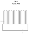
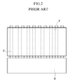
- Hereinafter, the connection structure of a prior art anisotropic conductive film is described in more detailed. According to Figures 1 and 2, an
electrode terminal 32 of theplasma display panel 30 is attached with the anisotropicconductive film 34. Then, the FPC terminal is introduced thereon, and the electrode of the plasma display panel and the terminal of the FPC are compressed to electrically connect the ball-type conductive metal particles dispersed in the conductive resin of the plasma display panel to the electrode of the plasma display panel and to the terminal of the FPC. - As shown in Figure 2, the anisotropic conductive film is attached by applying the anisotropic conductive film to the electrode terminal with the exception of the portion of the electrode terminal that connects with the plasma display panel and the portion of the electrode terminal to be connected with the FPC. In other words, the initial portion and the end portion of the terminal are not covered with the anisotropic conductive film. This prevents the aggregation of the conductive metal particles from the anisotropic conductive film on those portions of the electrode terminal when the anisotropic conductive film is expanded during the compressing process, preventing an electrical connection between the electrode of the plasma display panel and the terminal of the FPC in order to prevent a potential short circuit.
- However, the conductive resin of the anisotropic conductive film still flows out during the compression process and the conductive metal particles tend to aggregate at the initial and end portions of the electrode terminal which can result in a short circuit. Further, an excess of the conductive metal particles tend to aggregate at the gap portion instead of the electrode portion during the compression process. In general, about 30% of the conductive metal particles are present at the electrode with about 70% at the gap away from the electrode. As a result, electron movement is not facilitated between terminals due to the use of the conductive metal particles.
- In addition, in a plasma display device having such structure, the address electrode is mainly coated with silver. This can lead to a short circuit since air pockets, voids, and pores are generated due to impurities between the terminals, the low adhesive strength of the anisotropic conductive film, and since the micropores are generated in the anisotropic polymer of the anisotropic conductive film during the compression process. The problems also include migration that occurs due to the adhesive reinforcement of the electrode.
- One embodiment of the present invention provides a plasma display panel in which a connecting part is improved to have high adhesive and insulation properties. According to an embodiment of the present invention, the plasma display device includes a plasma display panel, a driving circuit for driving the plasma display panel, an electrical signal transmitting wire electrically connecting an electrode extended from the plasma display panel to the driving circuit, and an adhesive film interposed between the terminal of the electrical signal transmitting wire and the terminal of the electrode of the plasma display panel and connecting both terminals. In such an embodiment, the adhesive film includes an anisotropic conductive film including conductive particles.
- According to another embodiment of the present invention, the adhesive film includes an anisotropic conductive film including conductive particles and at least one insulated section referred to as a "dummy" the dummy being located either at the end of the anisotropic conductive film toward the plasma display panel, at the opposite end, or at both ends.
- According to yet another embodiment of the present invention, the adhesive film includes an anisotropic conductive comprising a plurality of conductive particles with insulated layers positioned on either side to form the anisotropic conductive film layer.
- Embodiments of the present invention are now described, by way of example and with reference to the accompanying drawings, of which:
- Figure 1 is a schematic view of a metal electrode of a plasma display panel device according to the prior art;
- Figure 2 is a schematic view of a metal electrode including an anisotropic conductive film according to the prior art;
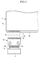
- Figure 3 is a schematic view of a metal electrode including an anisotropic conductive film according to an embodiment of the present invention;
- Figure 4 illustrates a process of equipping a metal electrode with an anisotropic conductive film according to another embodiment of the present invention;
- Figure 5 is a schematic view of a plasma display device according to an embodiment of the present invention; and
- Figure 6A to 6D are photographs showing address electrodes of plasma display devices according to Example 1 and Comparative Examples 1 to 3, respectively.
- An exemplary embodiment of the present invention will hereinafter be described in detail with reference to the accompanying drawings.
- The present invention relates to an adhesive film such as an anisotropic conductive film (ACF) connecting a metal bus electrode and an address electrode to an electrical signal transmitting wire such as FPC or TCP. According to an embodiment of the invention, the electrode is connected to the electrical signal transmitting wire using conductive particles provided in an adhesive film, but the conductive particles do not aggregate, and do not migrate by an excessive amount away from the electrode. This helps to prevent formation of an abnormal conductive path in order to facilitate electron transmission while preventing a short circuit.
- According to an embodiment of the present invention, the plasma display device includes a plasma display panel, a driving circuit for driving the plasma display panel, an electrical signal transmitting wire electrically connecting the electrode and extending from the plasma display panel to the driving circuit, and an adhesive film interposed between the terminal of the electrical signal wire and the terminal of the electrode of the plasma display panel, electrically connecting the terminals.
- According to an embodiment of the present invention, the adhesive film includes an anisotropic conductive film including conductive particles with an insulated dummy at least one of the terminal ends. The insulated dummy may be provided at an end of the anisotropic conductive film toward the plasma display panel, at the opposite end, or at both ends. As illustrated in Figure 3, a
plasma display panel 30 with anelectrode terminal 32 is provided as is known in the art. According to this embodiment, the anisotropicconductive film 36 is provided with a first insulated portion, or dummy 36b at the end of the anisotropicconductive film 36 toward the plasma display panel, and a second insulated portion, or dummy 36a at the opposite end of the anisotropicconductive film 36. - The insulated
dummies - The electrically insulated dummy may be a highly adhesive insulated polymer layer, which includes good adhesive properties, and may also be a humidity resisting polymer. Suitable polymers include, but are not limited to, epoxy resins, acryl resins, and acrylate resins.
- According to an embodiment of the invention, the adhesive film further includes an anisotropic film layer with conductive particles in its center portion. The conductive particles may include, but are not limited to, metal particles in which a metal such as nickel, copper, or silver is coated with a metal such as gold or palladium, or may include polymer particles substantially spherical in shape are coated with a metal such as gold or palladium. Examples of the polymer resin include, but are not limited to, polystyrene, polyacetylene, polymethylmethacrylate, polymethylethacrylate, and polythiophene.
- Suitable materials for the anisotropic conductive film layer include, but are not limited to, epoxy resin, acryl resin, and acrylate resin.
- The adhesive film according to another embodiment of the present invention includes an anisotropic conductive film layer comprising a plurality of conductive particles with insulating layers provided on either side.
- According to Figure 4, the anisotropic conductive film layer comprises a plurality of
conductive particles 20c withinsulating layers 20a on either side, the anisotropic conductive film layer being dispersed is placed between thedriving electrode 12 of theplasma display panel 11 and theterminals 10c of the electricalsignal transmitting wire 10. As further shown in Figure 4, the construct is compressed so that theconductive particles 20c are displaced between thedriving electrode 12 and theterminal 10c of the electricalsignal transmitting wire 10 and theconductive particles 20c are not present in thespaces driving electrodes 12 or theterminals 10c. - An adhesive film having a structure according to such an embodiment can efficiently prevent undesirable aggregation of the conductive particles.
- According to still another embodiment of the present invention, the adhesive film includes properties of both the two embodiments described above. The conductive particles are positioned within a pair of insulated layers, and dummy layers are provided on either end. Such an embodiment effectively controls the aggregation of the conductive particles and prevents the generation of air pockets and air bubbles caused by the low adhesive property of the adhesive film.
- Hereinafter, a plasma display device including an adhesive film according to an embodiment of the present invention is described with reference to the drawing figures.
- Figure 5 is a schematic view showing the connection between a panel-circuit of the plasma display device according to the present invention.
- According to an embodiment of the present invention, a plasma display panel 11 (PDP) includes a
driving electrode 12 extending between afront substrate 11a and aback substrate 11b. Thedriving electrode 12 is electrically connected to thedriving circuit 13 via an electricalsignal transmitting wire 10 such as a FPC and receives the signal required for driving the device from thedriving circuit 13. Thedriving electrode 12 is electrically connected to acorresponding driving circuit 13 via the corresponding electricalsignal transmitting wire 10. - The
driving circuit 13 is provided by equipping a circuit member on the Printed Circuit Board (PCB), and is equipped on the opposite surface to that of thePDP 11 on a chassis base. - Although the electrical signal transmitting wire may include the conventional FPC as illustrated in this specification, the present invention is not limited thereto, and may include a driver IC package such as a TCP.
- As shown in Figure 5, the driving
electrode 12 extends from thePDP 11 as the address electrode and is connected to the drivingcircuit 13 via the driver IC 10b. The driver IC 10b comprises the driver IC package together with the electricalsignal transmitting wire 10. - The driver IC 10b is mounted on the
FPC 10a of the electricalsignal transmitting wire 10. TheFPC 10a includes afirst connection 10d in which the terminal ends 10c that are electrically connected with the drivingelectrode 12 are exposed and asecond connection 10f in which the terminal ends 10e that are electrically connected to the drivingcircuit 13 are exposed. - The
first connection 10d is electrically connected to the drivingelectrode 12 with a film connection 20 interposed between the two. Thesecond connection 10f is electrically connected to thedriving wire 13 via aconnector 19 in a male/female connecting mode. - As described above, according to the adhesive film of the present invention, the plasma display device can prevent a short circuit between the panel electrode and the wire connection terminal of the FPC by improving the connection between the electrode of the plasma display panel and the FPC.
- The following examples illustrate the present invention in detail. However, it is understood that the present invention is not limited by these examples.
- The centre of an adhesive film was equipped with an anisotropic film layer including conductive particles of nickel coated with gold. With the adhesive film, the plasma display device was provided as shown in Figure 2.
- The plasma display device according to Example 1 was applied with DC 70V at a temperature of 60C and a relative humidity of 90% for 96 hours. A photograph of the surface of the address electrode was taken in order to evaluate the migration level, and the results are shown in Figure 6A. Photographs were taken of the surfaces of three different kinds of commercially available plasma display devices for Comparative Examples 1 to 3, and the results are shown in Figures 6B, 6C, and 6D.
- Figures 6A to 6D are photographs showing the colour of electrodes in which anisotropic film resin layers were present between electrodes. As shown in Figure 6A, the electrode was not corroded so that the white colour (or lightly shaded portions) was maintained, but a part of electrode surface was corroded to change the colour to brown (or darken the lightly shaded portions) as in Figures 6B to 6D. Particularly, dendrites developed due to the corrosion in Figures 6C and 6D. In other words, the plasma display device according to Example 1 did not generate the migration, but the migration was generated in all of Comparative Examples 1 to 3.
- As mentioned above, the plasma display device according to the present invention can prevent short circuits due to the aggregation of conductive particles by providing insulated dummies at the ends of the adhesive film connecting the electrode of the display panel and the electrical signal transmitting wire such as a TCF to improve the adhesive strength between the electrode and the electrical signal transmitting wire. This may be further accomplished by placing the conductive particles between a pair of insulating layers to form the adhesive film.
- While this invention has been described in connection with what is presently considered to be practical exemplary embodiments, it is to be understood that the invention is not limited to the disclosed embodiments, but, on the contrary, is intended to cover various modifications and equivalent arrangements included within the scope of the appended claims.
Claims (16)
- A plasma display device comprising:a plasma display panel;a driving circuit for driving the plasma display panel;an electrical signal transmitting wire for electrically connecting an electrode extending from the plasma display panel to the driving circuit; andan adhesive film electrically connecting a terminal end of the electrical signal transmitting wire and a terminal end of the electrode of the plasma display panel, wherein the adhesive film comprises:an anisotropic conductive film layer comprising a plurality of conductive particles; andat least one insulated portion disposed at one end of the anisotropic conductive film layer.
- The plasma display device of claim 1, wherein the at least one insulated portion comprises a highly adhesive insulated polymer material.
- The plasma display device of claim 2, wherein the highly adhesive insulated polymer material is selected from the group consisting of epoxy resins, acryl resins, and acrylate resins.
- The plasma display device of any of claims 1 to 3, wherein the conductive particles comprise metal particles or polymer particles.
- The plasma display device of any one of the preceding claims, wherein the conductive particles comprise particles coated with a metal coating, wherein the particles comprise a material selected from the group consisting of Ni, Cu, Au, Ag, and alloys thereof, and the metal coating comprises a material selected from the group consisting of Au and Pd.
- The plasma display device of any one of claims 1 to 4, wherein the conductive particles comprise polystyrene polymer particles coated with a metal selected from the group consisting of Au and Pd.
- The plasma display device of any one of the preceding claims, wherein the anisotropic conductive film layer comprises a material selected from the group consisting of epoxy resins, acryl resins, and acrylate resins.
- The plasma display device of any one of the preceding claims, wherein the conductive particles are positioned between a pair of insulating layers.
- The plasma display device of any one of the preceding claims, wherein the insulated portion is disposed at each end of the anisotropic conductive film layer.
- A plasma display device comprising:a plasma display panel;a driving circuit for driving the plasma display panel;an electrical signal transmitting wire for electrically connecting an electrode extending from the plasma display panel to the driving circuit; andan adhesive film electrically connecting a terminal end of the electrical signal transmitting wire and a terminal end of the electrode of the plasma display panel,wherein the adhesive film comprises an anisotropic conductive film layer comprising a sandwich structure having insulated layers spaced apart from one another by a layer of conductive particles.
- The plasma display device of claim 10, wherein the conductive particles comprise particles selected from metal particles and polymer particles.
- The plasma display device of claim 11, wherein the conductive particles comprise particles coated with a metal coating, wherein the particles comprise a material selected from the group consisting Ni, Cu, Au, Ag, and alloys thereof, and the metal coating comprises a metal selected from Au and Pd.
- The plasma display device of claim 11, wherein the conductive particles comprise polystyrene polymer particles coated with a metal selected from the group consisting of Au and Pd.
- The plasma display device of any one of claims 10 to 13, wherein the anisotropic conductive film layer comprises a material selected from the group consisting of epoxy resins, acryl resins, and acrylate resins.
- The plasma display device of any one of claims 10 to 14, further comprising at least one insulated dummy at at least one end of the anisotropic conductive film layer.
- The plasma display device of claim 15, further comprising an insulated dummy at each end of the anisotropic conductive film layer.
Applications Claiming Priority (1)
| Application Number | Priority Date | Filing Date | Title |
|---|---|---|---|
| KR1020050090000A KR100684726B1 (en) | 2005-09-27 | 2005-09-27 | Plasma display device |
Publications (2)
| Publication Number | Publication Date |
|---|---|
| EP1768215A2 true EP1768215A2 (en) | 2007-03-28 |
| EP1768215A3 EP1768215A3 (en) | 2009-10-21 |
Family
ID=37398319
Family Applications (1)
| Application Number | Title | Priority Date | Filing Date |
|---|---|---|---|
| EP06121218A Withdrawn EP1768215A3 (en) | 2005-09-27 | 2006-09-25 | Plasma Display Device |
Country Status (5)
| Country | Link |
|---|---|
| US (1) | US20070069984A1 (en) |
| EP (1) | EP1768215A3 (en) |
| JP (1) | JP2007094412A (en) |
| KR (1) | KR100684726B1 (en) |
| CN (1) | CN1941030A (en) |
Cited By (1)
| Publication number | Priority date | Publication date | Assignee | Title |
|---|---|---|---|---|
| CN102176337A (en) * | 2011-01-06 | 2011-09-07 | 天津大学 | Composite conductive particles for anisotropic conductive film and preparation method |
Families Citing this family (6)
| Publication number | Priority date | Publication date | Assignee | Title |
|---|---|---|---|---|
| KR100918052B1 (en) * | 2008-03-07 | 2009-09-22 | 삼성에스디아이 주식회사 | Plasma display device |
| JP4816750B2 (en) * | 2009-03-13 | 2011-11-16 | 住友電気工業株式会社 | Connection method of printed wiring board |
| CN102103428B (en) * | 2009-12-18 | 2013-01-02 | 群康科技(深圳)有限公司 | Flexible circuit board combining method of touch display device and touch display device |
| JP5458443B2 (en) * | 2010-09-14 | 2014-04-02 | 株式会社ジャパンディスプレイ | Display device with touch detection function and electronic device |
| DE102018102734A1 (en) * | 2018-01-18 | 2019-07-18 | Schreiner Group Gmbh & Co. Kg | Flexible electrical circuit with connection between electrically conductive structural elements |
| KR20220161358A (en) * | 2020-03-30 | 2022-12-06 | 쇼와덴코머티리얼즈가부시끼가이샤 | Adhesive composition and bonded structure |
Family Cites Families (24)
| Publication number | Priority date | Publication date | Assignee | Title |
|---|---|---|---|---|
| JPH03107888A (en) * | 1989-09-21 | 1991-05-08 | Sharp Corp | Connecting structure for circuit board |
| JPH03112732U (en) * | 1990-03-01 | 1991-11-18 | ||
| JPH04366630A (en) * | 1991-06-13 | 1992-12-18 | Sharp Corp | Anisotropic conductive adhesive tape |
| JPH05224229A (en) * | 1992-02-13 | 1993-09-03 | Casio Comput Co Ltd | Method for connecting liquid crystal display panel and circuit board |
| JPH0645024A (en) * | 1992-07-22 | 1994-02-18 | Hitachi Chem Co Ltd | Anisotropic conductive adhesive film |
| DE69325216T2 (en) * | 1992-09-08 | 1999-12-09 | Seiko Epson Corp., Tokio/Tokyo | Liquid crystal display device, device and method for assembling semiconductor elements and electronic printing device |
| JPH07318961A (en) * | 1994-05-27 | 1995-12-08 | Toshiba Corp | Electrical connection device |
| JP4282097B2 (en) * | 1994-06-15 | 2009-06-17 | 日立化成工業株式会社 | Circuit board connection method, connection structure, and adhesive film used therefor |
| JPH1067103A (en) * | 1996-08-28 | 1998-03-10 | Ricoh Co Ltd | Ink jet head, method for manufacturing the same, film adhesive and method for manufacturing the same |
| US6086441A (en) * | 1997-04-30 | 2000-07-11 | Matsushita Electric Industrial Co., Ltd. | Method for connecting electrodes of plasma display panel |
| JP3492195B2 (en) * | 1997-04-30 | 2004-02-03 | 松下電器産業株式会社 | Electrode bonding method for plasma display panel |
| JPH1197487A (en) * | 1997-09-25 | 1999-04-09 | Toshiba Corp | Mounting method and apparatus, and anisotropic conductive sheet |
| KR19990048959A (en) * | 1997-12-11 | 1999-07-05 | 김영환 | Liquid crystal panel |
| JP2000347592A (en) * | 1999-06-09 | 2000-12-15 | Fujitsu Ltd | Electrode terminal connection method for flat panel display |
| JP2001077501A (en) * | 1999-09-03 | 2001-03-23 | Seiko Epson Corp | Flexible wiring board, electro-optical device and electronic equipment |
| TW486721B (en) * | 2000-08-30 | 2002-05-11 | Acer Display Tech Inc | Plasma display having auxiliary bonding pad |
| JP3719925B2 (en) * | 2000-11-10 | 2005-11-24 | 松下電器産業株式会社 | Electrode bonding method for plasma display panel and plasma display panel |
| JP2002169172A (en) * | 2000-11-17 | 2002-06-14 | Internatl Business Mach Corp <Ibm> | Liquid crystal display panel, liquid crystal display panel manufacturing method, liquid crystal display device, liquid crystal display device manufacturing method, and bonded substrate |
| KR100385560B1 (en) * | 2000-12-27 | 2003-05-27 | 엘지전선 주식회사 | Conductive ball for anisotropic conductive film |
| JP2003195778A (en) * | 2001-12-25 | 2003-07-09 | Matsushita Electric Ind Co Ltd | Display device |
| JP2003283119A (en) * | 2002-03-22 | 2003-10-03 | Seiko Epson Corp | Image display device manufacturing method, image display device, and electronic apparatus |
| KR100559937B1 (en) * | 2003-01-08 | 2006-03-13 | 엘에스전선 주식회사 | Connection method of microcircuit and connection structure by it |
| JP3856233B2 (en) * | 2003-10-15 | 2006-12-13 | 日立化成工業株式会社 | Electrode connection method |
| KR100637429B1 (en) * | 2003-10-24 | 2006-10-20 | 삼성에스디아이 주식회사 | Plasma display device |
-
2005
- 2005-09-27 KR KR1020050090000A patent/KR100684726B1/en not_active Expired - Fee Related
-
2006
- 2006-09-25 EP EP06121218A patent/EP1768215A3/en not_active Withdrawn
- 2006-09-26 JP JP2006261535A patent/JP2007094412A/en active Pending
- 2006-09-26 US US11/528,186 patent/US20070069984A1/en not_active Abandoned
- 2006-09-27 CN CNA2006101447516A patent/CN1941030A/en active Pending
Cited By (2)
| Publication number | Priority date | Publication date | Assignee | Title |
|---|---|---|---|---|
| CN102176337A (en) * | 2011-01-06 | 2011-09-07 | 天津大学 | Composite conductive particles for anisotropic conductive film and preparation method |
| CN102176337B (en) * | 2011-01-06 | 2013-01-09 | 天津大学 | Composite conductive particles for anisotropic conductive film and preparation method |
Also Published As
| Publication number | Publication date |
|---|---|
| CN1941030A (en) | 2007-04-04 |
| JP2007094412A (en) | 2007-04-12 |
| KR100684726B1 (en) | 2007-02-20 |
| US20070069984A1 (en) | 2007-03-29 |
| EP1768215A3 (en) | 2009-10-21 |
Similar Documents
| Publication | Publication Date | Title |
|---|---|---|
| US6522073B2 (en) | Plasma display panel with an auxiliary bonding pad | |
| US20020014615A1 (en) | Anisotropic conductive adhesive film | |
| CN101136388A (en) | Chip film package and display panel assembly having the chip film package | |
| KR100637429B1 (en) | Plasma display device | |
| KR20100049668A (en) | Anisotropic conductive film and its production method, and bonded body employing anisotropic conductive film | |
| US20070069984A1 (en) | Plasma display device | |
| JP2004006417A (en) | Connecting element and connection structure of electrode using this | |
| US7452217B2 (en) | Connecting member for surface mounting circuit | |
| JPH11148058A (en) | Anisotropic conductive adhesive, liquid crystal display device and electronic equipment using the same | |
| JP7269885B2 (en) | Electrical connector manufacturing method | |
| JP4670859B2 (en) | Connection member and electrode connection structure using the same | |
| US7419387B2 (en) | Electric connection member utilizing ansiotropically conductive sheets | |
| KR100709249B1 (en) | Plasma display device | |
| JPS61242041A (en) | Semiconductor device | |
| KR100696629B1 (en) | Plasma display device | |
| JP3447569B2 (en) | Anisotropic conductive film and electrode connection structure using the same | |
| JP4572929B2 (en) | Connection member and electrode connection structure using the same | |
| KR20060110636A (en) | Plasma display device | |
| JP2008112732A (en) | Connecting method of electrode | |
| JP2009158833A (en) | Flexible printed wiring board connection structure | |
| JP4437459B2 (en) | Heat seal connector and connection method thereof | |
| EP1693876A2 (en) | Plasma display apparatus comprising connector | |
| JPS5821391A (en) | Device for mounting electronic part | |
| JP4670857B2 (en) | Repair property imparting method and connecting member | |
| JP4670858B2 (en) | Repair property imparting method and connecting member |
Legal Events
| Date | Code | Title | Description |
|---|---|---|---|
| PUAI | Public reference made under article 153(3) epc to a published international application that has entered the european phase |
Free format text: ORIGINAL CODE: 0009012 |
|
| 17P | Request for examination filed |
Effective date: 20060925 |
|
| AK | Designated contracting states |
Kind code of ref document: A2 Designated state(s): AT BE BG CH CY CZ DE DK EE ES FI FR GB GR HU IE IS IT LI LT LU LV MC NL PL PT RO SE SI SK TR |
|
| AX | Request for extension of the european patent |
Extension state: AL BA HR MK YU |
|
| RAP1 | Party data changed (applicant data changed or rights of an application transferred) |
Owner name: SAMSUNG SDI CO., LTD. |
|
| PUAL | Search report despatched |
Free format text: ORIGINAL CODE: 0009013 |
|
| AK | Designated contracting states |
Kind code of ref document: A3 Designated state(s): AT BE BG CH CY CZ DE DK EE ES FI FR GB GR HU IE IS IT LI LT LU LV MC NL PL PT RO SE SI SK TR |
|
| AX | Request for extension of the european patent |
Extension state: AL BA HR MK RS |
|
| AKX | Designation fees paid |
Designated state(s): DE FR GB HU NL |
|
| STAA | Information on the status of an ep patent application or granted ep patent |
Free format text: STATUS: THE APPLICATION HAS BEEN WITHDRAWN |
|
| 18W | Application withdrawn |
Effective date: 20100927 |