EP1763571B1 - Liquid crystalline interpenetrating polymer networks - Google Patents
Liquid crystalline interpenetrating polymer networks Download PDFInfo
- Publication number
- EP1763571B1 EP1763571B1 EP05734164A EP05734164A EP1763571B1 EP 1763571 B1 EP1763571 B1 EP 1763571B1 EP 05734164 A EP05734164 A EP 05734164A EP 05734164 A EP05734164 A EP 05734164A EP 1763571 B1 EP1763571 B1 EP 1763571B1
- Authority
- EP
- European Patent Office
- Prior art keywords
- use according
- photovoltaic cell
- electron
- polymer network
- group
- Prior art date
- Legal status (The legal status is an assumption and is not a legal conclusion. Google has not performed a legal analysis and makes no representation as to the accuracy of the status listed.)
- Expired - Lifetime
Links
Images

Classifications
-
- C—CHEMISTRY; METALLURGY
- C09—DYES; PAINTS; POLISHES; NATURAL RESINS; ADHESIVES; COMPOSITIONS NOT OTHERWISE PROVIDED FOR; APPLICATIONS OF MATERIALS NOT OTHERWISE PROVIDED FOR
- C09K—MATERIALS FOR MISCELLANEOUS APPLICATIONS, NOT PROVIDED FOR ELSEWHERE
- C09K19/00—Liquid crystal materials
- C09K19/04—Liquid crystal materials characterised by the chemical structure of the liquid crystal components, e.g. by a specific unit
- C09K19/06—Non-steroidal liquid crystal compounds
- C09K19/34—Non-steroidal liquid crystal compounds containing at least one heterocyclic ring
- C09K19/3441—Non-steroidal liquid crystal compounds containing at least one heterocyclic ring having nitrogen as hetero atom
- C09K19/3488—Non-steroidal liquid crystal compounds containing at least one heterocyclic ring having nitrogen as hetero atom the heterocyclic ring having more than 6 members, e.g. macrocycles, phthalocyanines
-
- C—CHEMISTRY; METALLURGY
- C09—DYES; PAINTS; POLISHES; NATURAL RESINS; ADHESIVES; COMPOSITIONS NOT OTHERWISE PROVIDED FOR; APPLICATIONS OF MATERIALS NOT OTHERWISE PROVIDED FOR
- C09K—MATERIALS FOR MISCELLANEOUS APPLICATIONS, NOT PROVIDED FOR ELSEWHERE
- C09K19/00—Liquid crystal materials
- C09K19/04—Liquid crystal materials characterised by the chemical structure of the liquid crystal components, e.g. by a specific unit
- C09K19/06—Non-steroidal liquid crystal compounds
- C09K19/32—Non-steroidal liquid crystal compounds containing condensed ring systems, i.e. fused, bridged or spiro ring systems
-
- C—CHEMISTRY; METALLURGY
- C09—DYES; PAINTS; POLISHES; NATURAL RESINS; ADHESIVES; COMPOSITIONS NOT OTHERWISE PROVIDED FOR; APPLICATIONS OF MATERIALS NOT OTHERWISE PROVIDED FOR
- C09K—MATERIALS FOR MISCELLANEOUS APPLICATIONS, NOT PROVIDED FOR ELSEWHERE
- C09K19/00—Liquid crystal materials
- C09K19/04—Liquid crystal materials characterised by the chemical structure of the liquid crystal components, e.g. by a specific unit
- C09K19/06—Non-steroidal liquid crystal compounds
- C09K19/34—Non-steroidal liquid crystal compounds containing at least one heterocyclic ring
- C09K19/3441—Non-steroidal liquid crystal compounds containing at least one heterocyclic ring having nitrogen as hetero atom
- C09K19/3477—Non-steroidal liquid crystal compounds containing at least one heterocyclic ring having nitrogen as hetero atom the heterocyclic ring being a five-membered aromatic ring containing at least one nitrogen atom
- C09K19/348—Non-steroidal liquid crystal compounds containing at least one heterocyclic ring having nitrogen as hetero atom the heterocyclic ring being a five-membered aromatic ring containing at least one nitrogen atom containing at least two nitrogen atoms
-
- C—CHEMISTRY; METALLURGY
- C09—DYES; PAINTS; POLISHES; NATURAL RESINS; ADHESIVES; COMPOSITIONS NOT OTHERWISE PROVIDED FOR; APPLICATIONS OF MATERIALS NOT OTHERWISE PROVIDED FOR
- C09K—MATERIALS FOR MISCELLANEOUS APPLICATIONS, NOT PROVIDED FOR ELSEWHERE
- C09K19/00—Liquid crystal materials
- C09K19/04—Liquid crystal materials characterised by the chemical structure of the liquid crystal components, e.g. by a specific unit
- C09K19/06—Non-steroidal liquid crystal compounds
- C09K19/34—Non-steroidal liquid crystal compounds containing at least one heterocyclic ring
- C09K19/3491—Non-steroidal liquid crystal compounds containing at least one heterocyclic ring having sulfur as hetero atom
- C09K19/3497—Non-steroidal liquid crystal compounds containing at least one heterocyclic ring having sulfur as hetero atom the heterocyclic ring containing sulfur and nitrogen atoms
-
- C—CHEMISTRY; METALLURGY
- C09—DYES; PAINTS; POLISHES; NATURAL RESINS; ADHESIVES; COMPOSITIONS NOT OTHERWISE PROVIDED FOR; APPLICATIONS OF MATERIALS NOT OTHERWISE PROVIDED FOR
- C09K—MATERIALS FOR MISCELLANEOUS APPLICATIONS, NOT PROVIDED FOR ELSEWHERE
- C09K19/00—Liquid crystal materials
- C09K19/04—Liquid crystal materials characterised by the chemical structure of the liquid crystal components, e.g. by a specific unit
- C09K19/38—Polymers
- C09K19/3833—Polymers with mesogenic groups in the side chain
- C09K19/3842—Polyvinyl derivatives
- C09K19/3852—Poly(meth)acrylate derivatives
- C09K19/3861—Poly(meth)acrylate derivatives containing condensed ring systems
-
- H—ELECTRICITY
- H10—SEMICONDUCTOR DEVICES; ELECTRIC SOLID-STATE DEVICES NOT OTHERWISE PROVIDED FOR
- H10K—ORGANIC ELECTRIC SOLID-STATE DEVICES
- H10K30/00—Organic devices sensitive to infrared radiation, light, electromagnetic radiation of shorter wavelength or corpuscular radiation
- H10K30/30—Organic devices sensitive to infrared radiation, light, electromagnetic radiation of shorter wavelength or corpuscular radiation comprising bulk heterojunctions, e.g. interpenetrating networks of donor and acceptor material domains
-
- H—ELECTRICITY
- H10—SEMICONDUCTOR DEVICES; ELECTRIC SOLID-STATE DEVICES NOT OTHERWISE PROVIDED FOR
- H10K—ORGANIC ELECTRIC SOLID-STATE DEVICES
- H10K85/00—Organic materials used in the body or electrodes of devices covered by this subclass
- H10K85/10—Organic polymers or oligomers
- H10K85/111—Organic polymers or oligomers comprising aromatic, heteroaromatic, or aryl chains, e.g. polyaniline, polyphenylene or polyphenylene vinylene
- H10K85/113—Heteroaromatic compounds comprising sulfur or selene, e.g. polythiophene
-
- H—ELECTRICITY
- H10—SEMICONDUCTOR DEVICES; ELECTRIC SOLID-STATE DEVICES NOT OTHERWISE PROVIDED FOR
- H10K—ORGANIC ELECTRIC SOLID-STATE DEVICES
- H10K85/00—Organic materials used in the body or electrodes of devices covered by this subclass
- H10K85/10—Organic polymers or oligomers
- H10K85/141—Organic polymers or oligomers comprising aliphatic or olefinic chains, e.g. poly N-vinylcarbazol, PVC or PTFE
-
- H—ELECTRICITY
- H10—SEMICONDUCTOR DEVICES; ELECTRIC SOLID-STATE DEVICES NOT OTHERWISE PROVIDED FOR
- H10K—ORGANIC ELECTRIC SOLID-STATE DEVICES
- H10K85/00—Organic materials used in the body or electrodes of devices covered by this subclass
- H10K85/60—Organic compounds having low molecular weight
- H10K85/649—Aromatic compounds comprising a hetero atom
- H10K85/655—Aromatic compounds comprising a hetero atom comprising only sulfur as heteroatom
-
- H—ELECTRICITY
- H10—SEMICONDUCTOR DEVICES; ELECTRIC SOLID-STATE DEVICES NOT OTHERWISE PROVIDED FOR
- H10K—ORGANIC ELECTRIC SOLID-STATE DEVICES
- H10K85/00—Organic materials used in the body or electrodes of devices covered by this subclass
- H10K85/731—Liquid crystalline materials
-
- C—CHEMISTRY; METALLURGY
- C09—DYES; PAINTS; POLISHES; NATURAL RESINS; ADHESIVES; COMPOSITIONS NOT OTHERWISE PROVIDED FOR; APPLICATIONS OF MATERIALS NOT OTHERWISE PROVIDED FOR
- C09K—MATERIALS FOR MISCELLANEOUS APPLICATIONS, NOT PROVIDED FOR ELSEWHERE
- C09K19/00—Liquid crystal materials
- C09K19/04—Liquid crystal materials characterised by the chemical structure of the liquid crystal components, e.g. by a specific unit
- C09K2019/0444—Liquid crystal materials characterised by the chemical structure of the liquid crystal components, e.g. by a specific unit characterized by a linking chain between rings or ring systems, a bridging chain between extensive mesogenic moieties or an end chain group
- C09K2019/0448—Liquid crystal materials characterised by the chemical structure of the liquid crystal components, e.g. by a specific unit characterized by a linking chain between rings or ring systems, a bridging chain between extensive mesogenic moieties or an end chain group the end chain group being a polymerizable end group, e.g. -Sp-P or acrylate
-
- C—CHEMISTRY; METALLURGY
- C09—DYES; PAINTS; POLISHES; NATURAL RESINS; ADHESIVES; COMPOSITIONS NOT OTHERWISE PROVIDED FOR; APPLICATIONS OF MATERIALS NOT OTHERWISE PROVIDED FOR
- C09K—MATERIALS FOR MISCELLANEOUS APPLICATIONS, NOT PROVIDED FOR ELSEWHERE
- C09K19/00—Liquid crystal materials
- C09K19/04—Liquid crystal materials characterised by the chemical structure of the liquid crystal components, e.g. by a specific unit
- C09K2019/0488—Liquid crystal materials characterised by the chemical structure of the liquid crystal components, e.g. by a specific unit characterized by a special bonding
- C09K2019/0496—Liquid crystal materials characterised by the chemical structure of the liquid crystal components, e.g. by a specific unit characterized by a special bonding the special bonding being a specific pi-conjugated group
-
- H—ELECTRICITY
- H10—SEMICONDUCTOR DEVICES; ELECTRIC SOLID-STATE DEVICES NOT OTHERWISE PROVIDED FOR
- H10K—ORGANIC ELECTRIC SOLID-STATE DEVICES
- H10K2102/00—Constructional details relating to the organic devices covered by this subclass
- H10K2102/10—Transparent electrodes, e.g. using graphene
- H10K2102/101—Transparent electrodes, e.g. using graphene comprising transparent conductive oxides [TCO]
- H10K2102/103—Transparent electrodes, e.g. using graphene comprising transparent conductive oxides [TCO] comprising indium oxides, e.g. ITO
-
- H—ELECTRICITY
- H10—SEMICONDUCTOR DEVICES; ELECTRIC SOLID-STATE DEVICES NOT OTHERWISE PROVIDED FOR
- H10K—ORGANIC ELECTRIC SOLID-STATE DEVICES
- H10K30/00—Organic devices sensitive to infrared radiation, light, electromagnetic radiation of shorter wavelength or corpuscular radiation
- H10K30/20—Organic devices sensitive to infrared radiation, light, electromagnetic radiation of shorter wavelength or corpuscular radiation comprising organic-organic junctions, e.g. donor-acceptor junctions
-
- H—ELECTRICITY
- H10—SEMICONDUCTOR DEVICES; ELECTRIC SOLID-STATE DEVICES NOT OTHERWISE PROVIDED FOR
- H10K—ORGANIC ELECTRIC SOLID-STATE DEVICES
- H10K30/00—Organic devices sensitive to infrared radiation, light, electromagnetic radiation of shorter wavelength or corpuscular radiation
- H10K30/50—Photovoltaic [PV] devices
-
- H—ELECTRICITY
- H10—SEMICONDUCTOR DEVICES; ELECTRIC SOLID-STATE DEVICES NOT OTHERWISE PROVIDED FOR
- H10K—ORGANIC ELECTRIC SOLID-STATE DEVICES
- H10K85/00—Organic materials used in the body or electrodes of devices covered by this subclass
- H10K85/10—Organic polymers or oligomers
- H10K85/111—Organic polymers or oligomers comprising aromatic, heteroaromatic, or aryl chains, e.g. polyaniline, polyphenylene or polyphenylene vinylene
- H10K85/113—Heteroaromatic compounds comprising sulfur or selene, e.g. polythiophene
- H10K85/1135—Polyethylene dioxythiophene [PEDOT]; Derivatives thereof
-
- H—ELECTRICITY
- H10—SEMICONDUCTOR DEVICES; ELECTRIC SOLID-STATE DEVICES NOT OTHERWISE PROVIDED FOR
- H10K—ORGANIC ELECTRIC SOLID-STATE DEVICES
- H10K85/00—Organic materials used in the body or electrodes of devices covered by this subclass
- H10K85/10—Organic polymers or oligomers
- H10K85/111—Organic polymers or oligomers comprising aromatic, heteroaromatic, or aryl chains, e.g. polyaniline, polyphenylene or polyphenylene vinylene
- H10K85/115—Polyfluorene; Derivatives thereof
-
- H—ELECTRICITY
- H10—SEMICONDUCTOR DEVICES; ELECTRIC SOLID-STATE DEVICES NOT OTHERWISE PROVIDED FOR
- H10K—ORGANIC ELECTRIC SOLID-STATE DEVICES
- H10K85/00—Organic materials used in the body or electrodes of devices covered by this subclass
- H10K85/30—Coordination compounds
- H10K85/321—Metal complexes comprising a group IIIA element, e.g. Tris (8-hydroxyquinoline) gallium [Gaq3]
- H10K85/324—Metal complexes comprising a group IIIA element, e.g. Tris (8-hydroxyquinoline) gallium [Gaq3] comprising aluminium, e.g. Alq3
-
- H—ELECTRICITY
- H10—SEMICONDUCTOR DEVICES; ELECTRIC SOLID-STATE DEVICES NOT OTHERWISE PROVIDED FOR
- H10K—ORGANIC ELECTRIC SOLID-STATE DEVICES
- H10K85/00—Organic materials used in the body or electrodes of devices covered by this subclass
- H10K85/60—Organic compounds having low molecular weight
- H10K85/615—Polycyclic condensed aromatic hydrocarbons, e.g. anthracene
- H10K85/621—Aromatic anhydride or imide compounds, e.g. perylene tetra-carboxylic dianhydride or perylene tetracarboxylic di-imide
-
- Y—GENERAL TAGGING OF NEW TECHNOLOGICAL DEVELOPMENTS; GENERAL TAGGING OF CROSS-SECTIONAL TECHNOLOGIES SPANNING OVER SEVERAL SECTIONS OF THE IPC; TECHNICAL SUBJECTS COVERED BY FORMER USPC CROSS-REFERENCE ART COLLECTIONS [XRACs] AND DIGESTS
- Y02—TECHNOLOGIES OR APPLICATIONS FOR MITIGATION OR ADAPTATION AGAINST CLIMATE CHANGE
- Y02E—REDUCTION OF GREENHOUSE GAS [GHG] EMISSIONS, RELATED TO ENERGY GENERATION, TRANSMISSION OR DISTRIBUTION
- Y02E10/00—Energy generation through renewable energy sources
- Y02E10/50—Photovoltaic [PV] energy
- Y02E10/549—Organic PV cells
-
- Y—GENERAL TAGGING OF NEW TECHNOLOGICAL DEVELOPMENTS; GENERAL TAGGING OF CROSS-SECTIONAL TECHNOLOGIES SPANNING OVER SEVERAL SECTIONS OF THE IPC; TECHNICAL SUBJECTS COVERED BY FORMER USPC CROSS-REFERENCE ART COLLECTIONS [XRACs] AND DIGESTS
- Y02—TECHNOLOGIES OR APPLICATIONS FOR MITIGATION OR ADAPTATION AGAINST CLIMATE CHANGE
- Y02P—CLIMATE CHANGE MITIGATION TECHNOLOGIES IN THE PRODUCTION OR PROCESSING OF GOODS
- Y02P70/00—Climate change mitigation technologies in the production process for final industrial or consumer products
- Y02P70/50—Manufacturing or production processes characterised by the final manufactured product
Definitions
- This invention relates to novel liquid crystalline blends and to uses thereof.
- Liquid crystalline polymer networks are formed by the in-situ polymerisation and crosslinking of thin films of small liquid crystal molecules (reactive mesogens).
- reactive mesogens generally comprise polymerisable groups, usually at the ends of flexible aliphatic spacers, the spacer molecules being attached to a more rigid aromatic core.
- liquid crystal polymer network will usually have a high birefringence which is spatially controlled to optimise the viewing angles of the liquid crystal display in the laptop and also to minimise unwanted birefringence colours.
- photovoltaic devices e.g. solar cells
- An essential requirement of photovoltaic devices, e.g. solar cells, is that they are capable of;
- each of these individual processes should be highly efficient and, most importantly, there should be a minimum of charge recombination.
- absorption usually occurs via exciton formation.
- Charge separation is achieved by ionisation of the exciton to form a free electron and hole at the interface between electron-donating and electron-accepting organics. This can occur either at a single hetero-interface or, more commonly, over a distributed interface obtained by phase separation of a blend of the two organic species.
- the electron is trapped in the electron accepting organics and the hole is trapped in the electron donating material.
- the different materials are phase separated so that the separated carriers occupy different regions as they drift to the external electrodes in the built-in field introduced by dissimilar electrodes. Hence recombination is avoided and an external photocurrent and photovoltage is produced.
- a power efficiency of approximately 3 % is among the best results to date obtained with a C 60 organic electron-acceptor dispersed in a main-chain polymer. 1
- main-chain polymer blends are their reluctance to mix on the required spatial scale of about 100 ⁇ . This requirement is due to the diffusion length of the exciton before recombination.
- the reluctance of main-chain polymer blends to mix greatly inhibits charge separation, which requires the exciton to encounter an interface before it can occur. This is a fundamental problem caused by the low entropy of mixing of main-chain polymers.
- There have been many attempts to minimise the phase separation e.g. by controlling the solvent evaporation rate, etc.
- Light emitting liquid crystalline polymers are known.
- US Patent Application No. 2003/018097 describes a process for forming a light emitting polymer wherein photopolymerisation is carried out using a reactive mesogen have an end group susceptible to a radical photopolymerisation process.
- US Patent Application No. 2003/0027017 describes a light emitter for a display comprising a cinnamate or coumarin chromophore attached to a side chain polymer backbone.
- liquid crystalline polymer networks hereinbefore described.
- they are capable of producing photovoltaic films in the form of robust polymer networks at low cost, with large surface area, which are capable of converting solar radiation to electrical power.
- the successful achievement has the potential for real wealth creation via an easily manufacturable, low-cost and completely new technology in the important area of renewable energy resources.
- Lower efficiency devices have many applications as low-cost, power supplies for consumer products.
- One advantage of the novel approach of the invention is the compatibility with flexible substrates, e.g., plastic substrates. Moreover, the formation of polymer networks from blends of reactive mesogens requires completely different conditions to those required for main-chain polymer blends.
- a photovoltaic cell comprising an interconnecting polymer network.
- Such light absorbing networks may have a variety of utilities, but they are especially useful in the manufacture of photovoltaic cells, e.g. solar cells.
- photovoltaic cells e.g. solar cells.
- Such photovoltaic cells may be reactive to light of a variety of wavelengths, e.g. ultra violet, infra-red, visible, etc.
- Electron-donating and electron-accepting reactive mesogens are intimately mixed as small molecules in the same liquid crystalline phase with no phase separation.
- a homogeneous crosslinked network is formed and retained by photopolymerisation or thermal polymerisation. Illumination with low light levels results in the trapping of electrons and holes by electron accepting and electron donating moieties respectively.
- the carriers drift/diffuse to the external electrodes. The carriers are not spatially separated so that efficiency decreases at high light levels because of the increased probability of electron and hole meeting and them recombining. It may be sufficient for one of the component of the blend to be a reactive mesogen.
- the second may be a main chain polymer or a small molecule.
- the electron-donating and electron-accepting reactive mesogens with different polymerisable end groups are intimately mixed as small molecules in the same liquid crystalline phase with no phase separation.
- Interpenetrating polymer networks are then formed either by irradiating with ultraviolet light or by thermal crosslinking.
- the different polymerisable end groups either polymerise at different rates or by the action of different initiators.
- an acrylate monomer reactive mesogen
- the diene monomer can then be polymerised by initiation with ultraviolet light.
- two interpenetrating polymer networks are formed with a large surface area of contact between them, which maximises charge separation. This procedure corresponds to nanophase separation and the spatial scale of the phase separation can be controlled over length scales from tens of As using different photoreactive groups, irradiation conditions, temperature, etc.
- a third device configuration results in a blend with completely continuous pathways from the electron-accepting material to the cathode and from the electron-donating material to the anode; no phase-separated island regions of one species, where carriers can be trapped, are formed.
- an electron-donating reactive mesogen and a non-polymerisable liquid crystal probably but not necessarily having the same aromatic core, are deposited from solution. They are intimately mixed as small molecules in the same liquid crystalline phase with no phase separation. Irradiation of the resultant thin film with ultraviolet light crosslinks the reactive mesogen to form a gel-like network and the polymerisable and nonpolymerisable liquid crystal phase-separate on a nanometre spatial scale. The same result can be obtained by thermal polymerization.
- the soluble liquid crystal is removed by washing with a suitable organic solvent so that a sponge like network of the hole transporting material penetrated with nanogrooves remains.
- the second step is the deposition, for example by spin-coating of an electron-accepting reactive mesogen, which fills the nanogrooves forming an interpenetrating polymer network of electron-donating and electron-accepting liquid crystals.
- Photopolymerisation or thermal polymerisation crosslinks the electron-accepting organic and forms a completely insoluble film.
- This configuration can be described as a vertically segregated blend or as a bilayer photovoltaic with a distributed interface.
- a main chain polymer or an electron-accepting molecular glass can be used for the top layer.
- a fourth device configuration gives an alternative approach to a vertically segregated blend. It can also be considered as a bilayer photovoltaic with a distributed interface.
- a thin film of the electron-donating material is deposited and partially crosslinked by thermal or photopolymerisation. Rinsing in an appropriate solvent removes some of the uncrosslinked material resulting in a nanogrooved surface with a large surface area.
- a distributed interface is formed when the electron-accepting material is deposited on top.
- a photovoltaic cell as hereinbefore described which is provided with a reflective coating on the rear side of the cell.
- Such reflective coating is suitable to reflect any transmitted light back through the cell, thus maximising the light absorption and hence the overall efficiency of the cell.
- interconnecting polymer networks may be suitable for the photovoltaic cell of the invention, we especially prefer the use of such interconnecting polymer networks as described in, for example, the prior art of US Patent Application No. 2003/018097 which is incorporated herein by reference.
- B-S-A-S-B (general formula I) wherein A is a chromophore; S is a spacer; and B is an end group which is susceptible to polymerisation.
- the polymerisation typically results in a light emitting polymer comprising arrangements of chromophores (e.g. uniaxially aligned) spaced by a crosslinked polymer backbone.
- chromophores e.g. uniaxially aligned
- Suitable chromophore (A) groups include fluorene, vinylenephenylene, anthracene, perylene, benzothiadiazole, oxadiazole, thiophene and any derivatives thereof.
- Suitable spacer (S) groups comprise organic chains, including e.g. flexible aliphatic, amine, ester or ether linkages.
- the chains may be saturated or unsaturated and be linear or branched. Aliphatic spacers are preferred.
- the presence of spacer groups aids the solubility and lowers the melting point of the light emitting polymer which assists the spin coating thereof.
- Suitable end groups are susceptible to photopolymerisation (e.g. by a radical process using UV radiation, generally unpolarized).
- the polymerisation involves cyclopolymerisation (i.e. the radical polymerisation step results in formation of a cyclic entity).
- a typical polymerisation process involves exposure of a reactive mesogen of general formula I to UV radiation to form an initial radical having the general formula as shown below: B-S-A-S-B ⁇ (general formula II) wherein A, S and B are as defined previously and B ⁇ is a radicalised end group which is capable of reacting with another B end group (particularly to form a cyclic entity).
- B. radicalised end group suitably comprises a bound radical such that the polymerisation process may be sterically controlled.
- Suitable end groups include dienes such as 1,4 1,5 and 1,6 dienes.
- the diene functionalities may be separated by aliphatic linkages, but other inert linkages including ether and amine linkages may also be employed.
- reaction typically involves cyclopolymerisation by a sequential intramolecular and intermolecular propagation: A ring structure is formed first by reaction of the free radical with the second double bond of the diene group. A double ring is obtained by the cyclopolymerisation which provides a particularly rigid backbone.
- the reaction is in general, sterically controlled.
- Exemplary reactive mesogens have the general formula: wherein R is:
- An exemplary reactive mesogen has the formula:
- the reactive mesogen typically has a molecular weight of from 200 to 2,000. Lower molecular weight monomers are preferred because their viscosity is also lower leading to enhanced spin coating characteristics and shorter annealing times which aids processing.
- the light emitting polymer network typically has a molecular weight of above 4,000, typically 4,000 to 15,000.
- the light absorbing and charge-transporting polymer typically comprises from 5 to 500, preferably from 10 to 300 monomeric units.
- a major advantage of polymer networks is that they can be manufactured using roll-to-roll processing.
- the resulting cling-film like sheets are robust, portable, flexible and transferable to almost any substrate by contact bonding and essentially cheap.
- Very recently the concept of "paintable" displays based on polymer networks has been introduced 3 . This could also be applied to photovoltaic polymer networks especially for use on non-planar surfaces, such as curved surfaces.
- liquid crystals and virtually all liquid crystalline polymer networks are manufactured for applications in transparent liquid crystal displays.
- the requirements for photovoltaics are substantially different: absorption covering the visible spectrum, reasonably high electron or hole mobility and appropriate energy-level alignment. Some of these reactive mesogens absorb light in the visible spectrum. It has also been shown that the liquid crystalline state leads to higher charge mobility than amorphous organic materials.
- the method of manufacturing the electron transporting reactive mesogens may be derived from, for example those described in US 2003/0018097 .
- Devices of type 1 can be made as follows.
- An InSnO(anode)/coated glass slide coated with a thin film of (PEDOT/PSS) can be used as a substrate.
- a 2 wt% mixture of an electron-donating and an electron-accepting reactive mesogen (for example a 1:1 mixture of 1 and 2 which is nematic at room temperature) was dissolved in chloroform and transferred via a syringe onto the substrate. The substrate was spun so that a thin film of the blend is formed. The solvent was evaporated and the reactive mesogens were photopolymerised by irradiation with ultraviolet radiation until the film becomes insoluble.
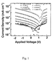
- the photovoltaic device was irradiated through the transparent substrate and anode at a wavelength(s) giving significant absorption, here 400 nm.
- An external quantum efficiency up to 3% and an open voltage > 1V was obtained depending on the input light intensity and wavelength as illustrated by Figure 1 . All other device types can be tested in the same way.
- Devices of type 2 can be prepared as follows. Device processing is carried out in an oxygen and water free environment. An InSnO/coated glass slide coated with a thin film of (PEDOT/PSS) was used as a substrate. A 2 wt% mixture of an electron-donating and an electron-accepting reactive mesogen (for example a 1:1 mixture of 3 and 2) was dissolved in chloroform and transferred via a syringe onto the substrate. The substrate was spun so that a thin film of the blend is formed. The solvent was then evaporated. Compound 3 was thermally polymerised by heating at 80°C for 30 minutes. On cooling 2 was photopolymerised by irradiation with ultraviolet radiation until the film becomes incompletely insoluble. A cathode, 5 ⁇ LiF/A1 was deposited by thermal evaporation.
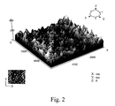
- Devices of type 3 can be prepared as follows. Device processing was carried out in an oxygen and water free environment. An InSnO/coated glass slide coated with a thin film of (PEDOT/PSS) was used as a substrate. A light-emitting gel was prepared by the polymerisation of a 1 wt% mixture of the non-polymerisable nematic compound 4 and the crosslinkable reactive mesogen 1 in the ratio 1:3. Both compounds are electron donating.
- the gel was heated to 60 °C and photopolymerised using light from a HeCd laser at 325 nm.
- the irradiation conditions for photopolymerisation depends on the UV light source and intensity.
- the gel was washed to remove the nonpolymerisable component from the surface of the gel and form a sponge-like network.
- Atomic force microscopy was used to image the sponge-like surface topography of the network on removal of the nonpolymerisable component. The image is shown in figure 2
- the spatial scale of the network can be modified by varying the polymerisation rate and the temperature at which photopolymerisation occurs.
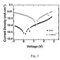
- An electron accepting material AlQ 3 which is a small molecular glass, of thickness approximately 30 nm, was deposited on top by thermal evaporation and a cathode deposited as above.
- Fig 3 shows the current- voltage characteristics of the photovoltaic device in the dark and on irradiation with light of intensity 2 mW cm -2 and wavelength 400 nm. A power conversion efficiency of 0.1 % was obtained.
- Devices of type 4 can be prepared as follows. Device processing was carried out in an oxygen and water free environment. An InSnO/coated glass slide coated with a thin film of (PEDOT/PSS) was used as a substrate. A 1 wt% mixture of the electron-donating reactive mesogen 1 was dissolved in chloroform and transferred via a syringe onto the substrate. The substrate was spun so that a thin film of the blend is formed. The solvent was evaporated and the reactive mesogen was photopolymerised by irradiation with ultraviolet radiation until the film is almost insoluble. (Typically, we used about 5/6 times the ultraviolet fluence required to obtain a completely insoluble layer.) The irradiation conditions for photopolymerisation depends on the UV light source and intensity.
- the film was washed to remove some of the unpolymerised monomer from the surface of the film
- Atomic force microscopy can be used to check the spatial scale of the nanogrooves formed, which can be modified by varying the polymerisation rate.
- An electron accepting material was deposited on top by spin-casting from a 1 wt% of solution 2 dissolved in chloroform and transferred via a syringe onto the gel. 2 was photopolymerised A cathode, for example 5 ⁇ LiF/A1 is deposited by thermal evaporation as a cathode.
- Figure 4 shows the current-voltage characteristic for different light intensities up to 1 mW cm -2 .
Landscapes
- Chemical & Material Sciences (AREA)
- Engineering & Computer Science (AREA)
- Materials Engineering (AREA)
- Crystallography & Structural Chemistry (AREA)
- Organic Chemistry (AREA)
- Physics & Mathematics (AREA)
- Electromagnetism (AREA)
- Spectroscopy & Molecular Physics (AREA)
- Photovoltaic Devices (AREA)
- Graft Or Block Polymers (AREA)
- Liquid Crystal Substances (AREA)
- Liquid Crystal (AREA)
- Addition Polymer Or Copolymer, Post-Treatments, Or Chemical Modifications (AREA)
- Polymers With Sulfur, Phosphorus Or Metals In The Main Chain (AREA)
Applications Claiming Priority (2)
| Application Number | Priority Date | Filing Date | Title |
|---|---|---|---|
| GBGB0407661.8A GB0407661D0 (en) | 2004-04-03 | 2004-04-03 | Liquid crystalline interpenetrating polymer networks |
| PCT/GB2005/001281 WO2005095543A2 (en) | 2004-04-03 | 2005-04-01 | Liquid crystalline interpenetrating polymer networks |
Publications (2)
| Publication Number | Publication Date |
|---|---|
| EP1763571A2 EP1763571A2 (en) | 2007-03-21 |
| EP1763571B1 true EP1763571B1 (en) | 2008-07-16 |
Family
ID=32247864
Family Applications (1)
| Application Number | Title | Priority Date | Filing Date |
|---|---|---|---|
| EP05734164A Expired - Lifetime EP1763571B1 (en) | 2004-04-03 | 2005-04-01 | Liquid crystalline interpenetrating polymer networks |
Country Status (7)
| Country | Link |
|---|---|
| US (1) | US7820907B2 (https=) |
| EP (1) | EP1763571B1 (https=) |
| JP (1) | JP5422119B2 (https=) |
| AT (1) | ATE401381T1 (https=) |
| DE (1) | DE602005008242D1 (https=) |
| GB (1) | GB0407661D0 (https=) |
| WO (1) | WO2005095543A2 (https=) |
Cited By (1)
| Publication number | Priority date | Publication date | Assignee | Title |
|---|---|---|---|---|
| CN107207709A (zh) * | 2015-04-14 | 2017-09-26 | 赫尔大学 | 聚合物网络 |
Families Citing this family (13)
| Publication number | Priority date | Publication date | Assignee | Title |
|---|---|---|---|---|
| WO2007064721A2 (en) | 2005-11-30 | 2007-06-07 | Aldred Matthew P | Lighting elements, devices and methods |
| JP5606912B2 (ja) * | 2007-09-03 | 2014-10-15 | メルク パテント ゲゼルシャフト ミット ベシュレンクテル ハフツング | フルオレン誘導体 |
| GB2456298A (en) | 2008-01-07 | 2009-07-15 | Anthony Ian Newman | Electroluminescent materials comprising oxidation resistant fluorenes |
| GB0802916D0 (en) | 2008-02-18 | 2008-03-26 | Newman Anthony I | Materials |
| US8173045B2 (en) | 2008-05-28 | 2012-05-08 | University Of Washington | Diels-Alder crosslinkable dendritic nonlinear optic chromophores and polymer composites |
| JP5531243B2 (ja) * | 2009-01-23 | 2014-06-25 | 三菱化学株式会社 | 半導体デバイスの製造方法及び太陽電池 |
| JP5326743B2 (ja) * | 2009-03-30 | 2013-10-30 | 大日本印刷株式会社 | 有機薄膜太陽電池及びその製造方法 |
| GB0917087D0 (en) | 2009-09-30 | 2009-11-11 | Lomox Ltd | Electroluminescent materials |
| JP5652092B2 (ja) * | 2010-09-30 | 2015-01-14 | 凸版印刷株式会社 | ブロック共重合体及びそれを用いた太陽電池 |
| GB201101094D0 (en) * | 2011-01-21 | 2011-03-09 | Univ Hull | Polymer networks |
| EP2921545B1 (en) * | 2014-03-21 | 2019-08-21 | Merck Patent GmbH | Polymerisable compounds and the use thereof in liquid-crystal displays |
| PL243899B1 (pl) | 2020-07-16 | 2023-10-30 | Univ Jagiellonski | System i sposób kalibracji czasowej układu detekcyjnego tomografu TOF-PET |
| US20230309328A1 (en) * | 2021-10-13 | 2023-09-28 | M and N Technology LLC | Liquid crystalline gel-based photovoltaic devices |
Family Cites Families (17)
| Publication number | Priority date | Publication date | Assignee | Title |
|---|---|---|---|---|
| GB9423692D0 (en) * | 1994-11-23 | 1995-01-11 | Philips Electronics Uk Ltd | A photoresponsive device |
| JPH1187064A (ja) * | 1997-09-08 | 1999-03-30 | Mitsubishi Electric Corp | 光電変換素子 |
| JP4043135B2 (ja) * | 1999-03-29 | 2008-02-06 | 株式会社東芝 | 機能素子および多成分多相系高分子成形体 |
| JP4558213B2 (ja) * | 1999-04-12 | 2010-10-06 | コーネル・リサーチ・ファンデーション・インコーポレイテッド | 疎水性および親水性の成分を有する水性ゲル形成システム |
| JP2001338273A (ja) * | 2000-05-25 | 2001-12-07 | Dainippon Printing Co Ltd | 積層発電表示型icカード |
| US20030235659A1 (en) * | 2000-11-30 | 2003-12-25 | Energy Sciences, Inc. | Particle beam processing apparatus |
| US20030018097A1 (en) * | 2001-07-03 | 2003-01-23 | O'neill Mary | Light emitting polymer |
| US6867243B2 (en) * | 2001-06-29 | 2005-03-15 | University Of Hull | Light emitting polymer |
| US6830831B2 (en) * | 2001-06-29 | 2004-12-14 | University Of Hull | Light emitter for a display |
| US7118787B2 (en) * | 2001-06-29 | 2006-10-10 | University Of Hull | Liquid crystal alignment layer |
| US20030021913A1 (en) * | 2001-07-03 | 2003-01-30 | O'neill Mary | Liquid crystal alignment layer |
| US20030027017A1 (en) * | 2001-07-03 | 2003-02-06 | O'neill Mary | Light emitter for a display |
| GB2379931B (en) * | 2001-08-17 | 2004-12-22 | Merck Patent Gmbh | Polymerisable dicyclohexylbenzenes |
| EP1318185B1 (en) | 2001-12-10 | 2005-02-16 | MERCK PATENT GmbH | Reactive mesogenic azulenes |
| EP1357163B1 (en) * | 2002-04-24 | 2006-05-31 | MERCK PATENT GmbH | Reactive mesogenic benzodithiophenes |
| DE60305570T2 (de) * | 2002-04-24 | 2007-05-03 | Merck Patent Gmbh | Reaktive mesogene Benzodithiophene |
| US20050116199A1 (en) * | 2003-04-09 | 2005-06-02 | Kelly Stephen M. | Crosslinkable materials for organic light emitting devices and methods |
-
2004
- 2004-04-03 GB GBGB0407661.8A patent/GB0407661D0/en not_active Ceased
-
2005
- 2005-04-01 JP JP2007505637A patent/JP5422119B2/ja not_active Expired - Fee Related
- 2005-04-01 AT AT05734164T patent/ATE401381T1/de not_active IP Right Cessation
- 2005-04-01 DE DE602005008242T patent/DE602005008242D1/de not_active Expired - Lifetime
- 2005-04-01 EP EP05734164A patent/EP1763571B1/en not_active Expired - Lifetime
- 2005-04-01 US US11/547,324 patent/US7820907B2/en not_active Expired - Fee Related
- 2005-04-01 WO PCT/GB2005/001281 patent/WO2005095543A2/en not_active Ceased
Cited By (1)
| Publication number | Priority date | Publication date | Assignee | Title |
|---|---|---|---|---|
| CN107207709A (zh) * | 2015-04-14 | 2017-09-26 | 赫尔大学 | 聚合物网络 |
Also Published As
| Publication number | Publication date |
|---|---|
| WO2005095543A3 (en) | 2005-11-24 |
| WO2005095543A2 (en) | 2005-10-13 |
| US20070284556A1 (en) | 2007-12-13 |
| JP5422119B2 (ja) | 2014-02-19 |
| EP1763571A2 (en) | 2007-03-21 |
| ATE401381T1 (de) | 2008-08-15 |
| JP2007531995A (ja) | 2007-11-08 |
| DE602005008242D1 (de) | 2008-08-28 |
| GB0407661D0 (en) | 2004-05-05 |
| US7820907B2 (en) | 2010-10-26 |
Similar Documents
| Publication | Publication Date | Title |
|---|---|---|
| EP1763571B1 (en) | Liquid crystalline interpenetrating polymer networks | |
| Zuniga et al. | Approaches to solution-processed multilayer organic light-emitting diodes based on cross-linking | |
| Botiz et al. | Optoelectronics using block copolymers | |
| Svensson et al. | High‐performance polymer solar cells of an alternating polyfluorene copolymer and a fullerene derivative | |
| Wantz et al. | Stabilizing polymer‐based bulk heterojunction solar cells via crosslinking | |
| Bacher et al. | Synthesis and characterization of photo-cross-linkable hole-conducting polymers | |
| CN102263205B (zh) | 可交联共轭聚合物材料在倒装有机光电器件中的应用 | |
| Cho et al. | Saturated and efficient red light-emitting fluorene-based alternating polymers containing phenothiazine derivatives | |
| Ego et al. | Attaching perylene dyes to polyfluorene: three simple, efficient methods for facile color tuning of light-emitting polymers | |
| Sommer et al. | Synthesis, purification, and characterization of well-defined all-conjugated diblock copolymers PF8TBT-b-P3HT | |
| Surin et al. | Correlation between the microscopic morphology and the solid-state photoluminescence properties in fluorene-based polymers and copolymers | |
| Bao et al. | Novel oxadiazole side chain conjugated polymers as single-layer light-emitting diodes with improved quantum efficiencies | |
| Tseng et al. | Stable organic blue-light-emitting devices prepared from poly [spiro (fluorene-9, 9 ‘-xanthene)] | |
| Carrasco‐Orozco et al. | New photovoltaic concept: liquid‐crystal solar cells using a nematic gel template | |
| Chen et al. | Effective end group modification of poly (3-hexylthiophene) with functional electron-deficient moieties for performance improvement in polymer solar cell | |
| Sun et al. | A holistic review of C= C crosslinkable conjugated molecules in solution‐processed organic electronics: insights into stability, processibility, and mechanical properties | |
| Gu et al. | Simultaneous performance and stability improvement of ternary polymer solar cells enabled by modulating the molecular packing of acceptors | |
| Ouhib et al. | Photovoltaic cells based on polythiophenes carrying lateral phenyl groups | |
| Suzuki et al. | Detrimental effects of “universal” singlet photocrosslinkers in organic photovoltaics | |
| KR20070034492A (ko) | 전자 디바이스 | |
| Sun et al. | Optimization of Organic Solar Cells in Both Space and Energy–Time Domains | |
| Guo et al. | Study of the dynamic process of enhancing the stability of conjugated polymer solutions and films induced by an external electric field | |
| KR102552323B1 (ko) | 페로브스카이트 태양전지 및 이의 제조방법 | |
| CN102391480A (zh) | 可交联的含氟苯封端的基于咔唑和双噻吩基取代的二氟苯并噻二唑的液晶共轭聚合物及其在太阳能电池中的应用 | |
| Gupta et al. | Band-gap tuning of pendant polymers for organic light-emitting devices and photovoltaic applications |
Legal Events
| Date | Code | Title | Description |
|---|---|---|---|
| PUAI | Public reference made under article 153(3) epc to a published international application that has entered the european phase |
Free format text: ORIGINAL CODE: 0009012 |
|
| 17P | Request for examination filed |
Effective date: 20061019 |
|
| AK | Designated contracting states |
Kind code of ref document: A2 Designated state(s): AT BE BG CH CY CZ DE DK EE ES FI FR GB GR HU IE IS IT LI LT LU MC NL PL PT RO SE SI SK TR |
|
| DAX | Request for extension of the european patent (deleted) | ||
| 17Q | First examination report despatched |
Effective date: 20070411 |
|
| GRAP | Despatch of communication of intention to grant a patent |
Free format text: ORIGINAL CODE: EPIDOSNIGR1 |
|
| GRAS | Grant fee paid |
Free format text: ORIGINAL CODE: EPIDOSNIGR3 |
|
| GRAA | (expected) grant |
Free format text: ORIGINAL CODE: 0009210 |
|
| AK | Designated contracting states |
Kind code of ref document: B1 Designated state(s): AT BE BG CH CY CZ DE DK EE ES FI FR GB GR HU IE IS IT LI LT LU MC NL PL PT RO SE SI SK TR |
|
| REG | Reference to a national code |
Ref country code: GB Ref legal event code: FG4D |
|
| REG | Reference to a national code |
Ref country code: CH Ref legal event code: EP |
|
| REF | Corresponds to: |
Ref document number: 602005008242 Country of ref document: DE Date of ref document: 20080828 Kind code of ref document: P |
|
| REG | Reference to a national code |
Ref country code: IE Ref legal event code: FG4D |
|
| REG | Reference to a national code |
Ref country code: CH Ref legal event code: NV Representative=s name: BRAUNPAT BRAUN EDER AG |
|
| NLV1 | Nl: lapsed or annulled due to failure to fulfill the requirements of art. 29p and 29m of the patents act | ||
| PG25 | Lapsed in a contracting state [announced via postgrant information from national office to epo] |
Ref country code: IS Free format text: LAPSE BECAUSE OF FAILURE TO SUBMIT A TRANSLATION OF THE DESCRIPTION OR TO PAY THE FEE WITHIN THE PRESCRIBED TIME-LIMIT Effective date: 20081116 Ref country code: NL Free format text: LAPSE BECAUSE OF FAILURE TO SUBMIT A TRANSLATION OF THE DESCRIPTION OR TO PAY THE FEE WITHIN THE PRESCRIBED TIME-LIMIT Effective date: 20080716 Ref country code: LT Free format text: LAPSE BECAUSE OF FAILURE TO SUBMIT A TRANSLATION OF THE DESCRIPTION OR TO PAY THE FEE WITHIN THE PRESCRIBED TIME-LIMIT Effective date: 20080716 |
|
| PG25 | Lapsed in a contracting state [announced via postgrant information from national office to epo] |
Ref country code: SI Free format text: LAPSE BECAUSE OF FAILURE TO SUBMIT A TRANSLATION OF THE DESCRIPTION OR TO PAY THE FEE WITHIN THE PRESCRIBED TIME-LIMIT Effective date: 20080716 Ref country code: ES Free format text: LAPSE BECAUSE OF FAILURE TO SUBMIT A TRANSLATION OF THE DESCRIPTION OR TO PAY THE FEE WITHIN THE PRESCRIBED TIME-LIMIT Effective date: 20081027 Ref country code: AT Free format text: LAPSE BECAUSE OF FAILURE TO SUBMIT A TRANSLATION OF THE DESCRIPTION OR TO PAY THE FEE WITHIN THE PRESCRIBED TIME-LIMIT Effective date: 20080716 Ref country code: BG Free format text: LAPSE BECAUSE OF FAILURE TO SUBMIT A TRANSLATION OF THE DESCRIPTION OR TO PAY THE FEE WITHIN THE PRESCRIBED TIME-LIMIT Effective date: 20081016 Ref country code: PT Free format text: LAPSE BECAUSE OF FAILURE TO SUBMIT A TRANSLATION OF THE DESCRIPTION OR TO PAY THE FEE WITHIN THE PRESCRIBED TIME-LIMIT Effective date: 20081216 Ref country code: FI Free format text: LAPSE BECAUSE OF FAILURE TO SUBMIT A TRANSLATION OF THE DESCRIPTION OR TO PAY THE FEE WITHIN THE PRESCRIBED TIME-LIMIT Effective date: 20080716 |
|
| PG25 | Lapsed in a contracting state [announced via postgrant information from national office to epo] |
Ref country code: BE Free format text: LAPSE BECAUSE OF FAILURE TO SUBMIT A TRANSLATION OF THE DESCRIPTION OR TO PAY THE FEE WITHIN THE PRESCRIBED TIME-LIMIT Effective date: 20080716 |
|
| PG25 | Lapsed in a contracting state [announced via postgrant information from national office to epo] |
Ref country code: DK Free format text: LAPSE BECAUSE OF FAILURE TO SUBMIT A TRANSLATION OF THE DESCRIPTION OR TO PAY THE FEE WITHIN THE PRESCRIBED TIME-LIMIT Effective date: 20080716 Ref country code: EE Free format text: LAPSE BECAUSE OF FAILURE TO SUBMIT A TRANSLATION OF THE DESCRIPTION OR TO PAY THE FEE WITHIN THE PRESCRIBED TIME-LIMIT Effective date: 20080716 |
|
| PLBE | No opposition filed within time limit |
Free format text: ORIGINAL CODE: 0009261 |
|
| STAA | Information on the status of an ep patent application or granted ep patent |
Free format text: STATUS: NO OPPOSITION FILED WITHIN TIME LIMIT |
|
| PG25 | Lapsed in a contracting state [announced via postgrant information from national office to epo] |
Ref country code: SK Free format text: LAPSE BECAUSE OF FAILURE TO SUBMIT A TRANSLATION OF THE DESCRIPTION OR TO PAY THE FEE WITHIN THE PRESCRIBED TIME-LIMIT Effective date: 20080716 Ref country code: RO Free format text: LAPSE BECAUSE OF FAILURE TO SUBMIT A TRANSLATION OF THE DESCRIPTION OR TO PAY THE FEE WITHIN THE PRESCRIBED TIME-LIMIT Effective date: 20080716 Ref country code: CZ Free format text: LAPSE BECAUSE OF FAILURE TO SUBMIT A TRANSLATION OF THE DESCRIPTION OR TO PAY THE FEE WITHIN THE PRESCRIBED TIME-LIMIT Effective date: 20080716 |
|
| 26N | No opposition filed |
Effective date: 20090417 |
|
| PG25 | Lapsed in a contracting state [announced via postgrant information from national office to epo] |
Ref country code: IT Free format text: LAPSE BECAUSE OF FAILURE TO SUBMIT A TRANSLATION OF THE DESCRIPTION OR TO PAY THE FEE WITHIN THE PRESCRIBED TIME-LIMIT Effective date: 20080716 |
|
| PG25 | Lapsed in a contracting state [announced via postgrant information from national office to epo] |
Ref country code: SE Free format text: LAPSE BECAUSE OF FAILURE TO SUBMIT A TRANSLATION OF THE DESCRIPTION OR TO PAY THE FEE WITHIN THE PRESCRIBED TIME-LIMIT Effective date: 20081016 |
|
| PG25 | Lapsed in a contracting state [announced via postgrant information from national office to epo] |
Ref country code: MC Free format text: LAPSE BECAUSE OF NON-PAYMENT OF DUE FEES Effective date: 20090430 |
|
| PG25 | Lapsed in a contracting state [announced via postgrant information from national office to epo] |
Ref country code: PL Free format text: LAPSE BECAUSE OF FAILURE TO SUBMIT A TRANSLATION OF THE DESCRIPTION OR TO PAY THE FEE WITHIN THE PRESCRIBED TIME-LIMIT Effective date: 20080716 |
|
| PG25 | Lapsed in a contracting state [announced via postgrant information from national office to epo] |
Ref country code: GR Free format text: LAPSE BECAUSE OF FAILURE TO SUBMIT A TRANSLATION OF THE DESCRIPTION OR TO PAY THE FEE WITHIN THE PRESCRIBED TIME-LIMIT Effective date: 20081017 |
|
| PG25 | Lapsed in a contracting state [announced via postgrant information from national office to epo] |
Ref country code: LU Free format text: LAPSE BECAUSE OF NON-PAYMENT OF DUE FEES Effective date: 20090401 |
|
| PG25 | Lapsed in a contracting state [announced via postgrant information from national office to epo] |
Ref country code: HU Free format text: LAPSE BECAUSE OF FAILURE TO SUBMIT A TRANSLATION OF THE DESCRIPTION OR TO PAY THE FEE WITHIN THE PRESCRIBED TIME-LIMIT Effective date: 20090117 |
|
| PG25 | Lapsed in a contracting state [announced via postgrant information from national office to epo] |
Ref country code: TR Free format text: LAPSE BECAUSE OF FAILURE TO SUBMIT A TRANSLATION OF THE DESCRIPTION OR TO PAY THE FEE WITHIN THE PRESCRIBED TIME-LIMIT Effective date: 20080716 |
|
| PG25 | Lapsed in a contracting state [announced via postgrant information from national office to epo] |
Ref country code: CY Free format text: LAPSE BECAUSE OF FAILURE TO SUBMIT A TRANSLATION OF THE DESCRIPTION OR TO PAY THE FEE WITHIN THE PRESCRIBED TIME-LIMIT Effective date: 20080716 |
|
| REG | Reference to a national code |
Ref country code: FR Ref legal event code: PLFP Year of fee payment: 12 |
|
| REG | Reference to a national code |
Ref country code: DE Ref legal event code: R082 Ref document number: 602005008242 Country of ref document: DE Representative=s name: SCHWABE SANDMAIR MARX PATENTANWAELTE RECHTSANW, DE Ref country code: DE Ref legal event code: R082 Ref document number: 602005008242 Country of ref document: DE Representative=s name: SSM SANDMAIR PATENTANWAELTE RECHTSANWALT PARTN, DE |
|
| REG | Reference to a national code |
Ref country code: FR Ref legal event code: PLFP Year of fee payment: 13 |
|
| PGFP | Annual fee paid to national office [announced via postgrant information from national office to epo] |
Ref country code: FR Payment date: 20170417 Year of fee payment: 13 Ref country code: GB Payment date: 20170412 Year of fee payment: 13 Ref country code: IE Payment date: 20170414 Year of fee payment: 13 Ref country code: DE Payment date: 20170427 Year of fee payment: 13 Ref country code: CH Payment date: 20170414 Year of fee payment: 13 |
|
| REG | Reference to a national code |
Ref country code: CH Ref legal event code: PCAR Free format text: NEW ADDRESS: HOLEESTRASSE 87, 4054 BASEL (CH) |
|
| REG | Reference to a national code |
Ref country code: DE Ref legal event code: R119 Ref document number: 602005008242 Country of ref document: DE |
|
| REG | Reference to a national code |
Ref country code: CH Ref legal event code: PL |
|
| GBPC | Gb: european patent ceased through non-payment of renewal fee |
Effective date: 20180401 |
|
| REG | Reference to a national code |
Ref country code: IE Ref legal event code: MM4A |
|
| PG25 | Lapsed in a contracting state [announced via postgrant information from national office to epo] |
Ref country code: DE Free format text: LAPSE BECAUSE OF NON-PAYMENT OF DUE FEES Effective date: 20181101 |
|
| PG25 | Lapsed in a contracting state [announced via postgrant information from national office to epo] |
Ref country code: LI Free format text: LAPSE BECAUSE OF NON-PAYMENT OF DUE FEES Effective date: 20180430 Ref country code: CH Free format text: LAPSE BECAUSE OF NON-PAYMENT OF DUE FEES Effective date: 20180430 Ref country code: GB Free format text: LAPSE BECAUSE OF NON-PAYMENT OF DUE FEES Effective date: 20180401 |
|
| PG25 | Lapsed in a contracting state [announced via postgrant information from national office to epo] |
Ref country code: FR Free format text: LAPSE BECAUSE OF NON-PAYMENT OF DUE FEES Effective date: 20180430 Ref country code: IE Free format text: LAPSE BECAUSE OF NON-PAYMENT OF DUE FEES Effective date: 20180401 |