EP1760042A2 - Procédé pour la réalisation de moyens de connexion et/ou de soudure d'un composant - Google Patents
Procédé pour la réalisation de moyens de connexion et/ou de soudure d'un composant Download PDFInfo
- Publication number
- EP1760042A2 EP1760042A2 EP06300836A EP06300836A EP1760042A2 EP 1760042 A2 EP1760042 A2 EP 1760042A2 EP 06300836 A EP06300836 A EP 06300836A EP 06300836 A EP06300836 A EP 06300836A EP 1760042 A2 EP1760042 A2 EP 1760042A2
- Authority
- EP
- European Patent Office
- Prior art keywords
- welding
- connection
- layer
- substrate
- production
- Prior art date
- Legal status (The legal status is an assumption and is not a legal conclusion. Google has not performed a legal analysis and makes no representation as to the accuracy of the status listed.)
- Granted
Links
Images


Classifications
-
- B—PERFORMING OPERATIONS; TRANSPORTING
- B81—MICROSTRUCTURAL TECHNOLOGY
- B81C—PROCESSES OR APPARATUS SPECIALLY ADAPTED FOR THE MANUFACTURE OR TREATMENT OF MICROSTRUCTURAL DEVICES OR SYSTEMS
- B81C1/00—Manufacture or treatment of devices or systems in or on a substrate
- B81C1/00015—Manufacture or treatment of devices or systems in or on a substrate for manufacturing microsystems
- B81C1/00261—Processes for packaging MEMS devices
- B81C1/00269—Bonding of solid lids or wafers to the substrate
-
- H—ELECTRICITY
- H05—ELECTRIC TECHNIQUES NOT OTHERWISE PROVIDED FOR
- H05K—PRINTED CIRCUITS; CASINGS OR CONSTRUCTIONAL DETAILS OF ELECTRIC APPARATUS; MANUFACTURE OF ASSEMBLAGES OF ELECTRICAL COMPONENTS
- H05K3/00—Apparatus or processes for manufacturing printed circuits
- H05K3/30—Assembling printed circuits with electric components, e.g. with resistors
- H05K3/32—Assembling printed circuits with electric components, e.g. with resistors electrically connecting electric components or wires to printed circuits
- H05K3/34—Assembling printed circuits with electric components, e.g. with resistors electrically connecting electric components or wires to printed circuits by soldering
- H05K3/3465—Application of solder
- H05K3/3478—Application of solder preforms; Transferring prefabricated solder patterns
-
- H—ELECTRICITY
- H10—SEMICONDUCTOR DEVICES; ELECTRIC SOLID-STATE DEVICES NOT OTHERWISE PROVIDED FOR
- H10W—GENERIC PACKAGES, INTERCONNECTIONS, CONNECTORS OR OTHER CONSTRUCTIONAL DETAILS OF DEVICES COVERED BY CLASS H10
- H10W72/00—Interconnections or connectors in packages
- H10W72/01—Manufacture or treatment
- H10W72/012—Manufacture or treatment of bump connectors, dummy bumps or thermal bumps
-
- B—PERFORMING OPERATIONS; TRANSPORTING
- B81—MICROSTRUCTURAL TECHNOLOGY
- B81C—PROCESSES OR APPARATUS SPECIALLY ADAPTED FOR THE MANUFACTURE OR TREATMENT OF MICROSTRUCTURAL DEVICES OR SYSTEMS
- B81C2201/00—Manufacture or treatment of microstructural devices or systems
- B81C2201/01—Manufacture or treatment of microstructural devices or systems in or on a substrate
- B81C2201/0101—Shaping material; Structuring the bulk substrate or layers on the substrate; Film patterning
- B81C2201/0147—Film patterning
- B81C2201/015—Imprinting
- B81C2201/0153—Imprinting techniques not provided for in B81C2201/0152
-
- B—PERFORMING OPERATIONS; TRANSPORTING
- B81—MICROSTRUCTURAL TECHNOLOGY
- B81C—PROCESSES OR APPARATUS SPECIALLY ADAPTED FOR THE MANUFACTURE OR TREATMENT OF MICROSTRUCTURAL DEVICES OR SYSTEMS
- B81C2203/00—Forming microstructural systems
- B81C2203/01—Packaging MEMS
- B81C2203/0172—Seals
- B81C2203/019—Seals characterised by the material or arrangement of seals between parts
-
- H—ELECTRICITY
- H05—ELECTRIC TECHNIQUES NOT OTHERWISE PROVIDED FOR
- H05K—PRINTED CIRCUITS; CASINGS OR CONSTRUCTIONAL DETAILS OF ELECTRIC APPARATUS; MANUFACTURE OF ASSEMBLAGES OF ELECTRICAL COMPONENTS
- H05K2203/00—Indexing scheme relating to apparatus or processes for manufacturing printed circuits covered by H05K3/00
- H05K2203/01—Tools for processing; Objects used during processing
- H05K2203/0104—Tools for processing; Objects used during processing for patterning or coating
- H05K2203/0113—Female die used for patterning or transferring, e.g. temporary substrate having recessed pattern
-
- H—ELECTRICITY
- H05—ELECTRIC TECHNIQUES NOT OTHERWISE PROVIDED FOR
- H05K—PRINTED CIRCUITS; CASINGS OR CONSTRUCTIONAL DETAILS OF ELECTRIC APPARATUS; MANUFACTURE OF ASSEMBLAGES OF ELECTRICAL COMPONENTS
- H05K2203/00—Indexing scheme relating to apparatus or processes for manufacturing printed circuits covered by H05K3/00
- H05K2203/04—Soldering or other types of metallurgic bonding
- H05K2203/0405—Solder foil, tape or wire
-
- H—ELECTRICITY
- H05—ELECTRIC TECHNIQUES NOT OTHERWISE PROVIDED FOR
- H05K—PRINTED CIRCUITS; CASINGS OR CONSTRUCTIONAL DETAILS OF ELECTRIC APPARATUS; MANUFACTURE OF ASSEMBLAGES OF ELECTRICAL COMPONENTS
- H05K2203/00—Indexing scheme relating to apparatus or processes for manufacturing printed circuits covered by H05K3/00
- H05K2203/04—Soldering or other types of metallurgic bonding
- H05K2203/043—Reflowing of solder coated conductors, not during connection of components, e.g. reflowing solder paste
-
- H—ELECTRICITY
- H05—ELECTRIC TECHNIQUES NOT OTHERWISE PROVIDED FOR
- H05K—PRINTED CIRCUITS; CASINGS OR CONSTRUCTIONAL DETAILS OF ELECTRIC APPARATUS; MANUFACTURE OF ASSEMBLAGES OF ELECTRICAL COMPONENTS
- H05K3/00—Apparatus or processes for manufacturing printed circuits
- H05K3/02—Apparatus or processes for manufacturing printed circuits in which the conductive material is applied to the surface of the insulating support and is thereafter removed from such areas of the surface which are not intended for current conducting or shielding
- H05K3/06—Apparatus or processes for manufacturing printed circuits in which the conductive material is applied to the surface of the insulating support and is thereafter removed from such areas of the surface which are not intended for current conducting or shielding the conductive material being removed chemically or electrolytically, e.g. by photo-etch process
- H05K3/061—Etching masks
- H05K3/062—Etching masks consisting of metals or alloys or metallic inorganic compounds
-
- H—ELECTRICITY
- H10—SEMICONDUCTOR DEVICES; ELECTRIC SOLID-STATE DEVICES NOT OTHERWISE PROVIDED FOR
- H10W—GENERIC PACKAGES, INTERCONNECTIONS, CONNECTORS OR OTHER CONSTRUCTIONAL DETAILS OF DEVICES COVERED BY CLASS H10
- H10W72/00—Interconnections or connectors in packages
- H10W72/01—Manufacture or treatment
- H10W72/012—Manufacture or treatment of bump connectors, dummy bumps or thermal bumps
- H10W72/01204—Manufacture or treatment of bump connectors, dummy bumps or thermal bumps using temporary auxiliary members, e.g. using sacrificial coatings or handle substrates
-
- H—ELECTRICITY
- H10—SEMICONDUCTOR DEVICES; ELECTRIC SOLID-STATE DEVICES NOT OTHERWISE PROVIDED FOR
- H10W—GENERIC PACKAGES, INTERCONNECTIONS, CONNECTORS OR OTHER CONSTRUCTIONAL DETAILS OF DEVICES COVERED BY CLASS H10
- H10W72/00—Interconnections or connectors in packages
- H10W72/01—Manufacture or treatment
- H10W72/012—Manufacture or treatment of bump connectors, dummy bumps or thermal bumps
- H10W72/01231—Manufacture or treatment of bump connectors, dummy bumps or thermal bumps using blanket deposition
-
- H—ELECTRICITY
- H10—SEMICONDUCTOR DEVICES; ELECTRIC SOLID-STATE DEVICES NOT OTHERWISE PROVIDED FOR
- H10W—GENERIC PACKAGES, INTERCONNECTIONS, CONNECTORS OR OTHER CONSTRUCTIONAL DETAILS OF DEVICES COVERED BY CLASS H10
- H10W72/00—Interconnections or connectors in packages
- H10W72/01—Manufacture or treatment
- H10W72/012—Manufacture or treatment of bump connectors, dummy bumps or thermal bumps
- H10W72/01251—Changing the shapes of bumps
-
- H—ELECTRICITY
- H10—SEMICONDUCTOR DEVICES; ELECTRIC SOLID-STATE DEVICES NOT OTHERWISE PROVIDED FOR
- H10W—GENERIC PACKAGES, INTERCONNECTIONS, CONNECTORS OR OTHER CONSTRUCTIONAL DETAILS OF DEVICES COVERED BY CLASS H10
- H10W72/00—Interconnections or connectors in packages
- H10W72/20—Bump connectors, e.g. solder bumps or copper pillars; Dummy bumps; Thermal bumps
-
- H—ELECTRICITY
- H10—SEMICONDUCTOR DEVICES; ELECTRIC SOLID-STATE DEVICES NOT OTHERWISE PROVIDED FOR
- H10W—GENERIC PACKAGES, INTERCONNECTIONS, CONNECTORS OR OTHER CONSTRUCTIONAL DETAILS OF DEVICES COVERED BY CLASS H10
- H10W72/00—Interconnections or connectors in packages
- H10W72/90—Bond pads, in general
- H10W72/921—Structures or relative sizes of bond pads
- H10W72/923—Bond pads having multiple stacked layers
-
- H—ELECTRICITY
- H10—SEMICONDUCTOR DEVICES; ELECTRIC SOLID-STATE DEVICES NOT OTHERWISE PROVIDED FOR
- H10W—GENERIC PACKAGES, INTERCONNECTIONS, CONNECTORS OR OTHER CONSTRUCTIONAL DETAILS OF DEVICES COVERED BY CLASS H10
- H10W72/00—Interconnections or connectors in packages
- H10W72/90—Bond pads, in general
- H10W72/941—Dispositions of bond pads
- H10W72/9415—Dispositions of bond pads relative to the surface, e.g. recessed, protruding
-
- H—ELECTRICITY
- H10—SEMICONDUCTOR DEVICES; ELECTRIC SOLID-STATE DEVICES NOT OTHERWISE PROVIDED FOR
- H10W—GENERIC PACKAGES, INTERCONNECTIONS, CONNECTORS OR OTHER CONSTRUCTIONAL DETAILS OF DEVICES COVERED BY CLASS H10
- H10W72/00—Interconnections or connectors in packages
- H10W72/90—Bond pads, in general
- H10W72/941—Dispositions of bond pads
- H10W72/944—Dispositions of multiple bond pads
- H10W72/9445—Top-view layouts, e.g. mirror arrays
-
- H—ELECTRICITY
- H10—SEMICONDUCTOR DEVICES; ELECTRIC SOLID-STATE DEVICES NOT OTHERWISE PROVIDED FOR
- H10W—GENERIC PACKAGES, INTERCONNECTIONS, CONNECTORS OR OTHER CONSTRUCTIONAL DETAILS OF DEVICES COVERED BY CLASS H10
- H10W72/00—Interconnections or connectors in packages
- H10W72/90—Bond pads, in general
- H10W72/951—Materials of bond pads
- H10W72/952—Materials of bond pads comprising metals or metalloids, e.g. PbSn, Ag or Cu
-
- Y—GENERAL TAGGING OF NEW TECHNOLOGICAL DEVELOPMENTS; GENERAL TAGGING OF CROSS-SECTIONAL TECHNOLOGIES SPANNING OVER SEVERAL SECTIONS OF THE IPC; TECHNICAL SUBJECTS COVERED BY FORMER USPC CROSS-REFERENCE ART COLLECTIONS [XRACs] AND DIGESTS
- Y10—TECHNICAL SUBJECTS COVERED BY FORMER USPC
- Y10T—TECHNICAL SUBJECTS COVERED BY FORMER US CLASSIFICATION
- Y10T29/00—Metal working
- Y10T29/49—Method of mechanical manufacture
- Y10T29/49002—Electrical device making
- Y10T29/49117—Conductor or circuit manufacturing
- Y10T29/49124—On flat or curved insulated base, e.g., printed circuit, etc.
- Y10T29/49155—Manufacturing circuit on or in base
-
- Y—GENERAL TAGGING OF NEW TECHNOLOGICAL DEVELOPMENTS; GENERAL TAGGING OF CROSS-SECTIONAL TECHNOLOGIES SPANNING OVER SEVERAL SECTIONS OF THE IPC; TECHNICAL SUBJECTS COVERED BY FORMER USPC CROSS-REFERENCE ART COLLECTIONS [XRACs] AND DIGESTS
- Y10—TECHNICAL SUBJECTS COVERED BY FORMER USPC
- Y10T—TECHNICAL SUBJECTS COVERED BY FORMER US CLASSIFICATION
- Y10T29/00—Metal working
- Y10T29/49—Method of mechanical manufacture
- Y10T29/49002—Electrical device making
- Y10T29/49117—Conductor or circuit manufacturing
- Y10T29/49124—On flat or curved insulated base, e.g., printed circuit, etc.
- Y10T29/49155—Manufacturing circuit on or in base
- Y10T29/49158—Manufacturing circuit on or in base with molding of insulated base
Definitions
- the invention relates to the field of microelectronics, and more specifically that of hybridization techniques and welding or sealing fusible welding material.
- chip hybridization by means of conducting solder balls on multilayer substrates, intended to achieve interconnections between the chips.
- This technology better known by the Anglo-Saxon “ flip-chip”, allows to hybridize hundreds of chips on ceramic substrates.
- conductive microbeads generally made of a low melting point material, such as SnPb, In, AgCuSn, and is now widely controlled.
- microcomponents are encapsulated within a structure of the type housing or protective cover or equivalent, to provide protection against shocks, corrosion, rays electromagnetic parasites etc ...
- housings or protective covers also provide the possibility for these microcomponents to work under vacuum, or under a controlled atmosphere (pressure, neutral gas, etc.) or in a sealed manner with respect to the ambient atmosphere.
- Such a housing or cover is conventionally sealed by means of a seal or sealing bead, based on the periphery of the component in question, generally at a wettable area or surface, also called gripping surface.
- micro-sensors whether micro-sensors, micro-actuators, MEMS (micro electro mechanical system), etc ..., require for their implementation the implementation of welding elements and / or connection of different heights, measured with respect to a reference consisting of the upper face of the substrate on which are placed or reported the microcomponents in question.
- MEMS micro electro mechanical system
- the object of the present invention is precisely to overcome the implementation of two consecutive steps to allow the realization of welding elements of different height, and corollary, at a reduced manufacturing cost.
- the present invention is directed to a method for producing means of connection and / or welding or sealing, of a component present on a substrate.
- the invention consists neither more nor less than to implement during the manufacturing process a step of molding a sufficiently ductile material to allow its deformation, especially at room temperature, as technologies widely known coin hitting, or at a temperature close to the melting temperature of said material, or even at a temperature above the latter.
- the height of the layer of ductile material previously deposited is sufficient to allow proper stamping by the matrix, and corollary the realization of different material heights.
- the layer of ductile material is deposited on surfaces or wettability zones previously produced on the substrate receiving the component or microcomponent.
- these zones or wettability surfaces are made of gold after the production of a barrier layer typically made of nickel.
- these zones or wettability surfaces are produced exactly according to the desired profile of the welding or connection means, ie occupy a surface on the substrate substantially corresponding to the occupied surface. on the same substrate by the connection and / or solder elements resulting from the method of the invention.
- these zones or wettability surfaces cover the entirety of the substrate, and the layer intended to constitute these wettability surfaces is removed from the substrate between the zones receiving the ductile material by etching, after deposition. said ductile material layer, the latter acting as a mask during the operation of etching the constituent layer of the wettability surfaces.
- the ductile material is imparted after formatting or stamping, a shape corresponding to the desired shape by reflow at a temperature above the melting temperature of the ductile material.
- a substrate 1 typically made of silicon.
- This substrate is for example made of a wafer or wafer according to the English expression devoted, a size of 300 mm for example.
- This material is ductile, and typically consists of indium or a tin / lead alloy, or an AgCuSn alloy.
- a stamping step is then carried out (FIG. 1b) by means of a die 3 provided with punches 4, or whose forms 7, 8 formed therein define between them punches 4 (see FIG. 2 and FIG. 3a). .
- This matrix operates by indexing: the matrix is in this case the size of a photocomposition field; it is applied to each field and is indexed at the step of the field ("step and repeat " process).
- this matrix can also operate in a whole slice in a global mode: the matrix is then of the same size as the substrate plate or wafer 1, and the stamping operation is carried out in a single operation.
- the die 3 is actuated by an automatic or manual press to stamp according to the arrow 5 said layer of ductile material 2.
- the lower wall of the forms 7, 8 and the underside of the matrix are coated with a release layer, for example made of PTFE (polytetrafluoroethylene), and then said matrix is applied to the surface of the layer. of ductile material 2 to be printed with a pressure P 4. The matrix is then removed thereby defining a succession of shapes, depending on the shapes 7 and 8 of said matrix.
- a release layer for example made of PTFE (polytetrafluoroethylene)
- This matrix is advantageously made of silicon. Indeed, it can be seen that the use of such a material makes it possible to obtain patterns of great fineness, thereby making it possible to reduce the cost of producing molds by conventional photolithography and chemical etching, and in particular by producing Naturally trapezoid-shaped patterns favoring demolding operations.
- the balls are shaped in the conventional manner by reflowing the soldering elements, that is to say by raising the temperature to a temperature higher than the melting temperature of said ductile material.
- the ball-shaped is adopted, or when a weld bead is used, a substantially circular section results from the reflow.
- a barrier layer of nickel is made, in particular by electroless, at the level of open studs as a result of the foundry operations leading to the realization of the CMOS wafer. silicon.
- This nickel barrier layer is coated with a gold layer (gold acting as a bonding metal, and therefore a wettability surface) and this, according to methods known elsewhere and as for example developed by PACTECH. .
- the first consists in the realization of this double layer nickel / gold at the only final places of positioning of the welding elements, whether it is a cord or microbeads ( Figure 2).
- the wettability zones are pre-treated and the deposition and formatting or stamping operation of the layer of ductile material 2 intended to form the soldering or connection elements is carried out as previously described.
- the entire upper surface of the wafer is coated with the nickel / gold layer 10.
- etching is carried out by removing the double nickel / gold barrier layer at the zones without these solder elements.
- this etching is followed by a second etching, which removes the barrier layer between the shapes.
- CMOS wafer 15 at the silicon casting output of 300 mm by 300 mm. It comprises a number of aluminum pads 16 , so conductive, spaced 100 microns from each other and distributed around the periphery of the wafer.
- the surface of the chip is 1cm 2 , and the height of the pads of 50 ⁇ m.
- connection beads for hermetic seals are also perfectly feasible, in particular for the implementation of cover or protective casing for the hermetic confinement of the component.
- the invention also applies to the preparation of hybridization beads and generally to the production of all the hybridized components, whether they are components operating in the field of optics, X-rays, or hybridization on flexible ribbon, on ceramic, on " multi chip module ", on board: COB “ chip on board” (printed circuit) or on COG “ chip on glass ".
Landscapes
- Engineering & Computer Science (AREA)
- Manufacturing & Machinery (AREA)
- Microelectronics & Electronic Packaging (AREA)
- Wire Bonding (AREA)
- Micromachines (AREA)
- Electric Connection Of Electric Components To Printed Circuits (AREA)
- Combinations Of Printed Boards (AREA)
Abstract
- à déposer sur ledit substrat 1 une couche 2 en un matériau ductile, le cas échéant, conducteur de l'électricité ;
- à emboutir la couche 2 ainsi réalisée au moyen d'une matrice gravée 3, dont les gravures sont fonction de la forme que l'on souhaite conférer auxdits moyens de connexion et/ou de soudure.


Description
- L'invention concerne le domaine de la microélectronique, et plus spécifiquement celui des techniques d'hybridation et de soudure ou de scellement par matériau de soudure fusible.
- L'évolution de la technologie des circuits intégrés a permis d'aboutir à la miniaturisation poussée et notamment à réaliser des microcomposants.
- Parmi les progrès techniques ayant permis une telle miniaturisation, figure l'hybridation de puces au moyen de billes de soudure conductrices sur des substrats multicouches, destinés à réaliser des interconnections entre les puces. Cette technologie, mieux connue sous l'expression anglo-saxonne « flip-chip », permet ainsi d'hybrider des centaines de puces sur des substrats céramiques.
- Elle met en oeuvre des microbilles conductrices, en général réalisées en un matériau à bas point de fusion, tel que SnPb, In, AgCuSn, et est aujourd'hui largement maîtrisée.
- Dans le même domaine, mais dans une application différente, un certain nombre de ces microcomposants sont encapsulés au sein d'une structure de type boîtier ou capot de protection ou équivalent, permettant d'assurer une protection contre les chocs, la corrosion, les rayons électromagnétiques parasites etc...
- Au surplus, de tels boîtiers ou capots de protection assurent également la possibilité pour ces microcomposants de travailler sous vide, ou sous atmosphère contrôlée (pression, gaz neutre, etc..) ou de manière étanche par rapport à l'atmosphère ambiante.
- Un tel boîtier ou capot est classiquement scellé au moyen d'un joint ou cordon de scellement, rapporté à la périphérie du composant en question, en général au niveau d'une zone ou surface de mouillabilité, également dénommée surface d'accroche.
- Plus fréquemment, les composants concernés, qu'il s'agisse de micro-capteurs, micro-actuateurs, MEMS (micro electro mechanical system), etc..., nécessitent donc pour leur réalisation la mise en oeuvre d'éléments de soudure et/ou de connexion de hauteurs différentes, mesurées par rapport à un référentiel constitué par la face supérieure du substrat sur lequel sont mis en place ou rapportés les microcomposants en question.
- Plusieurs technologies sont aujourd'hui connues, qui permettent la réalisation de tels cordons de soudure ou le dépôt de billes ou microbilles d'hybridation, et donc de connexion.
- On peut ainsi les techniques suivantes :
- évaporation à travers un masque et soudure ;
- « solder jetting » ou jet de gouttelettes de soudure à l'instar des imprimantes à jet d'encre :;
- électrolyse;
- sérigraphie.
- Cependant, toutes ces techniques nécessitent systématiquement au moins deux opérations différentes pour aboutir à des éléments de soudure et de connexion de hauteur différente.
- Au surplus, la plupart de ces technologies s'avère d'un coût de réalisation élevé, notamment en raison des manipulations qu'elles engendrent.
- L'objet de la présente invention est justement de s'affranchir de la mise en oeuvre de deux étapes consécutives pour permettre la réalisation d'éléments de soudure de hauteur différente, et corollairement, selon un coût de fabrication réduit.
- Ainsi, la présente invention vise un procédé de réalisation de moyens de connexion et/ou de soudure ou de scellement, d'un composant présent sur un substrat.
- Ce procédé consiste :
- à déposer sur ledit substrat une couche en un matériau ductile, le cas échéant, conducteur de l'électricité ;
- à emboutir la couche ainsi réalisée au moyen d'une matrice gravée, dont les gravures sont fonction de la forme que l'on souhaite conférer auxdits moyens de connexion et/ou de soudure.
- En d'autres termes, l'invention consiste ni plus ni moins qu'à mettre en oeuvre durant le procédé de réalisation une étape de moulage d'un matériau suffisamment ductile pour permettre sa déformation, notamment à température ambiante à l'instar des technologies largement connues de frappage des pièces de monnaie, ou à une température proche de la température de fusion dudit matériau, voire même à une température supérieure à cette dernière.
- En effet, il convient de conférer à la matrice d'emboutissage ou de frappage les formes souhaitées, et notamment les profondeurs différentes souhaitées pour permettre d'aboutir à des hauteurs différenciées des moyens de soudure ou de connexion.
- Bien évidemment, la hauteur de la couche de matériau ductile préalablement déposée est suffisante pour permettre un emboutissage correct par la matrice, et corollairement la réalisation de hauteurs de matériau différentes.
- Selon une caractéristique de l'invention, la couche en matériau ductile est déposée sur des surfaces ou zones de mouillabilité préalablement réalisées sur le substrat recevant le composant ou microcomposant. Typiquement, ces zones ou surfaces de mouillabilité sont réalisées en or après réalisation d'une couche barrière typiquement réalisée en nickel.
- Selon une première forme de réalisation de l'invention, ces zones ou surfaces de mouillabilité sont réalisées exactement en fonction du profil souhaité des moyens de soudure ou de connexion, c'est à dire occupent une surface sur le substrat correspondant sensiblement à la surface occupée sur le même substrat par les éléments de connexion et/ou de soudure résultant du procédé de l'invention.
- Selon une autre forme de réalisation de l'invention, ces zones ou surfaces de mouillabilité recouvrent l'intégralité du substrat, et la couche destinée à constituer ces surfaces de mouillabilité est ôtée du substrat entre les zones recevant le matériau ductile par gravure, après dépôt de ladite couche en matériau ductile, ce dernier faisant fonction de masque lors de l'opération de gravure de la couche constitutive des surfaces de mouillabilité.
- Enfin, et selon l'invention, on confère au matériau ductile après formatage ou frappage, une forme correspondante à la forme souhaitée par refusion sous une température supérieure à la température de fusion du matériau ductile.
- Notamment, par ce biais, on confère une forme en billes ou, lorsque l'on souhaite disposer d'un cordon de scellement, on confère une forme globalement cylindrique à la couche de matériau ductile ainsi déposée.
- La manière dont l'invention peut être réalisée et les avantages qui en découlent ressortiront mieux des exemples de réalisation qui suivent donnés à titre indicatif et non limitatif à l'appui des figures annexées.
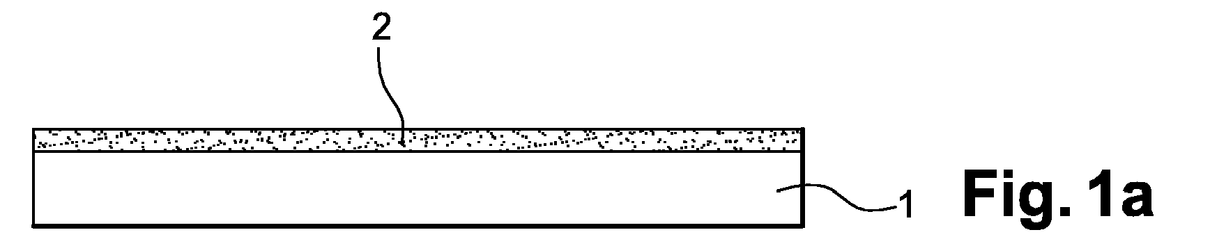
- Les figures 1a à 1d sont des représentations schématiques du principe mis en oeuvre par la présente invention.
- La figure 2 est une représentation schématique en section visant à illustrer l'étape de frappage de matériau ductile selon une première forme de réalisation.
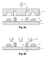
- Les figures 3a et 3b sont des vues analogues à la figure 2, mais d'une autre forme de réalisation.
- Les figures 4a à 4e sont des représentations schématiques respectivement vues de dessus (figure 4a) et en section (figures 4b à 4d) de la mise en oeuvre du procédé de l'invention pour la fabrication de billes sur un wafer CMOS.
- On a donc schématiquement représenté en relation avec les figures 1a à 1d le principe général sous-tendant le procédé conforme à l'invention.
- Selon celui-ci, on dispose d'un substrat 1 typiquement réalisé en silicium. Ce substrat est par exemple constitué d'une galette ou wafer selon l'expression anglo-saxonne consacrée, d'une dimension de 300 mm par exemple.
- Puis on procède au dépôt ou au report d'une couche d'un matériau de soudure 2 sur une tranche. Ce matériau est ductile, et est typiquement constitué d'indium ou d'un alliage étain/plomb, ou d'un alliage AgCuSn.
- On procède alors à une étape d'emboutissage (figure 1b) au moyen d'une matrice 3 pourvue de poinçons 4, ou dont les formes 7, 8 ménagées en son sein définissent entre elles des poinçons 4 (voir figure 2 et figure 3a).
- Cette matrice fonctionne par indexation : la matrice est dans ce cas de la taille d'un champ de photocomposition ; elle est appliquée sur chaque champ et est indexée au pas du champ (procédé « step and repeat »).
- Cependant, cette matrice peut aussi fonctionner selon une tranche entière selon un mode global : la matrice est alors de la même taille que la plaque de substrat ou wafer 1, et l'opération d'emboutissage est réalisée en une seule opération.
- La matrice 3 est actionnée par une presse automatique ou manuelle pour venir emboutir selon la flèche 5 ladite couche de matériau ductile 2.
- A cet effet, on enduit la paroi inférieure des formes 7, 8 ainsi que la face inférieure de la matrice d'une couche anti-adhésive, par exemple réalisée en PTFE (polytétrafluoroéthylène), puis on applique ladite matrice sur la surface de la couche de matériau ductile 2 à imprimer avec une pression P 4. On retire alors la matrice définissant ainsi une succession de formes, fonction des formes 7 et 8 de ladite matrice.
- Cette matrice est avantageusement réalisée en silicium. En effet, on observe que la mise en oeuvre d'un tel matériau permet d'aboutir à des motifs d'une grande finesse, permettant ce faisant un coût de réalisation réduit des moules par photolithographie et gravure chimique classiques, et notamment la réalisation de motifs naturellement en forme de trapèze, favorisant les opérations de démoulage.
- Après l'opération de démoulage, certaines zones en creux sont susceptibles de présenter des résidus issus de soudure, que l'on ôte par gravure.
- Enfin (figure 1d) on remet les billes en forme de manière classique par refusion des éléments de soudure, c'est-à-dire par élévation de la température selon une température supérieure à la température de fusion dudit matériau ductile.
- Par phénomène naturelle de réduction de la tension superficielle, la forme en bille est adoptée, ou, lorsque l'on met en oeuvre un cordon de soudure, une section sensiblement circulaire résulte de la refusion.
- Cependant et la plupart du temps, les éléments de soudure, qu'il s'agisse de cordon de scellement ou de billes ou microbilles de conduction, également de scellement, sont rapportés sur une surface ou zone de mouillabilité.
- Pour ce faire, préalablement au dépôt de la couche de soudure 2 on procède à la réalisation d'une couche barrière en nickel, notamment par voie électroless, au niveau de plots ouverts en suite des opérations de fonderie aboutissant à la réalisation du wafer CMOS en silicium.
- On rapporte sur cette couche barrière en nickel une couche d'or (l'or faisant fonction de métal d'accroche, donc de surface de mouillabilité) et ce, selon des procédés connus par ailleurs et tel que par exemple développé par la société PACTECH.
- Selon l'invention, deux alternatives sont possibles. La première consiste en la réalisation de cette double couche nickel/or au niveau des seuls lieux définitifs de positionnement des éléments de soudure, qu'il s'agisse d'un cordon ou de microbilles (figure 2).
- Dans ce cas, les zones de mouillabilité sont prégravées et l'opération de dépôt et de formatage ou de frappage de la couche de matériau ductile 2 destiné à constituer les éléments de soudure ou de connexion s'effectue tel que précédemment décrit.
- Selon une autre forme de réalisation représentée en relation avec les figures 3a et 3b, toute la surface supérieure du wafer, à l'exception bien évidemment de celle destinée à recevoir le composant ou le microcomposant, est revêtu de la couche nickel/or 10. Dans ce cas, après frappage de la couche de matériau ductile 2 selon la forme souhaitée, on procède par gravure à l'enlèvement de la double couche barrière nickel/or au niveau des zones dépourvues de ces éléments de soudure.
- Dans les deux cas, il est possible que subsiste après l'étape d'emboutissage, une pellicule de matériau ductile entre les formes réalisées. Il faut alors prévoir une étape de gravure de ces résidus. A cet effet, toute la surface est rafraîchie par gravure d'une fine couche du matériau ductile, tant sur les formes qu'entre les formes.
- Dans la seconde forme de réalisation, cette gravure est suivie par une seconde gravure, qui supprime la couche barrière entre les formes.
- On a décrit en relation avec la figure 4 un mode plus précis de réalisation de l'invention. Celui-ci met en oeuvre un wafer CMOS 15 en sortie de fonderie silicium de 300 mm sur 300 mm. Il comporte un certain nombre de plots d'aluminium 16, donc conducteurs, espacés de 100 µm les uns des autres et répartis à la périphérie du wafer. La surface de la puce est de 1cm2, et la hauteur des plots de 50µm.
- Ainsi, pour une puce de 1 cm de coté (surface = 108 µm2), on dépose une couche d'indium de 1,8 µm d'épaisseur. Ce faisant, on dispose d'un volume de matériau ductile de 1,8 . 108 µm3. Cette puce est alors emboutie par une matrice dessinée afin d'obtenir 1000 plots de 60 x 60 µm. La soudure passant pratiquement entièrement dans les plots, ces derniers ont une hauteur d'environ 50 µm.
- On observe donc tout l'intérêt du procédé conforme à l'invention dans la mesure où, en une seule opération, il est possible d'obtenir les éléments de soudure de taille différente, ce que l'on ne savait pas faire jusqu'alors. Au surplus, les techniques de mise en oeuvre, et notamment l'impression directe, mais également l'évaporation électrolyse permettent de ne pas obérer les coûts de revient de tels composants.
- Ce faisant, la fabrication des microcomposants actifs, notamment électroniques, est envisageable par ce procédé, et notamment les matrices de détection de rayonnements électromagnétiques, et plus particulièrement infrarouges, munies ou non de compensation de dilatation inhérent au changement de température de fonctionnement.
- Les cordons de scellement réalisés concomitamment avec les billes de connexion pour les scellements hermétiques sont également parfaitement réalisables, notamment pour la mise en oeuvre de capot ou boîtier de protection pour le confinement hermétique du composant.
- Enfin l'invention s'applique également à la préparation des billes d'hybridation et de manière générale à la réalisation de tous les composants hybridés, qu'il s'agisse de composants fonctionnant dans le domaine de l'optique, des rayons X, ou de l'hybridation sur ruban flexible, sur céramique, sur « multi chip module », sur board : COB « chip on board » (circuit imprimé) ou sur verre COG « chip on glass ».
Claims (8)
- Procédé pour la réalisation de moyens de connexion et/ou de soudure ou de scellement, d'un composant présent sur un substrat 1, caractérisé en ce qu'il consiste :- à déposer sur ledit substrat 1 une couche 2 en un matériau ductile, le cas échéant, conducteur de l'électricité ;- à emboutir la couche 2 ainsi réalisée au moyen d'une matrice gravée 3, dont les gravures sont fonction de la forme que l'on souhaite conférer auxdits moyens de connexion et/ou de soudure.
- Procédé pour la réalisation de moyens de connexion et/ou de soudure ou de scellement, d'un composant selon la revendication 1, caractérisé en ce qu'il est procédé à une étape de gravure du matériau résiduel entre les formes ainsi réalisées.
- Procédé pour la réalisation de moyens de connexion et/ou de soudure ou de scellement, d'un composant selon l'une des revendications 1 et 2, caractérisé en ce que les profondeurs des gravures réalisées au sein de la matrice sont identiques ou différentes.
- Procédé pour la réalisation de moyens de connexion et/ou de soudure ou de scellement, d'un composant selon l'une des revendications 1 à 3, caractérisé en ce que la couche 2 en matériau ductile est déposée sur des surfaces ou zones de mouillabilité 10 préalablement réalisées sur le substrat 1 recevant le composant.
- Procédé pour la réalisation de moyens de connexion et/ou de soudure ou de scellement, d'un composant selon la revendication 4, caractérisé en ce que les zones ou surfaces de mouillabilité 10 sont réalisées en or après réalisation d'une couche barrière typiquement réalisée en nickel.
- Procédé pour la réalisation de moyens de connexion et/ou de soudure ou de scellement, d'un composant selon l'une des revendications 4 et 5, caractérisé en ce que les zones ou surfaces de mouillabilité 10 sont réalisées en fonction du profil souhaité des moyens de soudure ou de connexion, et en ce qu'elles occupent une surface sur le substrat correspondant sensiblement à la surface occupée sur le même substrat par les éléments de connexion et/ou de soudure résultant dudit procédé.
- Procédé pour la réalisation de moyens de connexion et/ou de soudure ou de scellement, d'un composant selon l'une des revendications 4 et 5, caractérisé en ce que les zones ou surfaces de mouillabilité 10 sont réalisées de telle manière à recouvrir l'intégralité du substrat 1, et en ce que la ou les couches destinées à constituer ces zones ou surfaces de mouillabilité 10 sont ôtées du substrat entre les zones recevant le matériau ductile par gravure, après dépôt de ladite couche 2 en matériau ductile, ce dernier faisant fonction de masque lors de l'opération de gravure de la couche constitutive des surfaces de mouillabilité.
- Procédé pour la réalisation de moyens de connexion et/ou de soudure ou de scellement, d'un composant selon l'une des revendications 1 à 7, caractérisé en ce que la forme souhaitée des éléments de connexion et/ou de soudure est conférée par opération de refusion sous une température supérieure à la température de fusion du matériau ductile.
Applications Claiming Priority (1)
| Application Number | Priority Date | Filing Date | Title |
|---|---|---|---|
| FR0552611A FR2890066B1 (fr) | 2005-08-30 | 2005-08-30 | Procede pour la realisation de moyens de connexion et/ou de soudure d'un composant |
Publications (3)
| Publication Number | Publication Date |
|---|---|
| EP1760042A2 true EP1760042A2 (fr) | 2007-03-07 |
| EP1760042A3 EP1760042A3 (fr) | 2010-08-11 |
| EP1760042B1 EP1760042B1 (fr) | 2013-05-29 |
Family
ID=36601185
Family Applications (1)
| Application Number | Title | Priority Date | Filing Date |
|---|---|---|---|
| EP06300836.1A Not-in-force EP1760042B1 (fr) | 2005-08-30 | 2006-07-28 | Procédé pour la réalisation de moyens de connexion et/ou de soudure d'un composant |
Country Status (4)
| Country | Link |
|---|---|
| US (1) | US7509733B2 (fr) |
| EP (1) | EP1760042B1 (fr) |
| JP (1) | JP5019824B2 (fr) |
| FR (1) | FR2890066B1 (fr) |
Families Citing this family (3)
| Publication number | Priority date | Publication date | Assignee | Title |
|---|---|---|---|---|
| FR2876193B1 (fr) * | 2004-10-04 | 2007-01-26 | Commissariat Energie Atomique | Dispositif nanoimprime comportant des motifs metalliques et procede de nanoimpression de motifs metalliques |
| DE112011102924T5 (de) | 2010-09-03 | 2013-07-18 | Ntn Corporation | Lagerbaugruppe mit Rotationssensor |
| CN110740597A (zh) * | 2019-10-14 | 2020-01-31 | Oppo广东移动通信有限公司 | 壳体及制备方法、电子设备 |
Family Cites Families (5)
| Publication number | Priority date | Publication date | Assignee | Title |
|---|---|---|---|---|
| US2757443A (en) * | 1953-01-21 | 1956-08-07 | Erie Resistor Corp | Method of making printed circuits |
| US2955351A (en) * | 1954-12-28 | 1960-10-11 | Plast O Fab Circuits Inc | Method of making a printed circuit |
| FR2705832B1 (fr) * | 1993-05-28 | 1995-06-30 | Commissariat Energie Atomique | Procédé de réalisation d'un cordon d'étanchéité et de tenue mécanique entre un substrat et une puce hybridée par billes sur le substrat. |
| US5547902A (en) * | 1995-01-18 | 1996-08-20 | Advanced Micro Devices, Inc. | Post hot working process for semiconductors |
| JP2005191133A (ja) * | 2003-12-24 | 2005-07-14 | Ngk Spark Plug Co Ltd | 配線基板の製造方法および配線基板 |
-
2005
- 2005-08-30 FR FR0552611A patent/FR2890066B1/fr not_active Expired - Fee Related
-
2006
- 2006-07-28 EP EP06300836.1A patent/EP1760042B1/fr not_active Not-in-force
- 2006-08-14 US US11/503,856 patent/US7509733B2/en not_active Expired - Fee Related
- 2006-08-22 JP JP2006224827A patent/JP5019824B2/ja not_active Expired - Fee Related
Also Published As
| Publication number | Publication date |
|---|---|
| JP5019824B2 (ja) | 2012-09-05 |
| US7509733B2 (en) | 2009-03-31 |
| US20070049065A1 (en) | 2007-03-01 |
| FR2890066A1 (fr) | 2007-03-02 |
| EP1760042A3 (fr) | 2010-08-11 |
| FR2890066B1 (fr) | 2007-09-21 |
| JP2007073951A (ja) | 2007-03-22 |
| EP1760042B1 (fr) | 2013-05-29 |
Similar Documents
| Publication | Publication Date | Title |
|---|---|---|
| US9034729B2 (en) | Semiconductor device and method of manufacturing the same | |
| EP1108677B1 (fr) | Procédé d'encapsulation hermétique in situ de microsystèmes | |
| EP2175485B1 (fr) | Connexion par emboitement de deux inserts soudés et sa méthode de fabrication | |
| EP2213616B1 (fr) | Procédé de fermeture de cavité pour au moins un dispositif microélectronique | |
| US7485956B2 (en) | Microelectronic package optionally having differing cover and device thermal expansivities | |
| EP2255383B1 (fr) | Composant de connexion muni d'inserts creux et son procede de realisation | |
| FR2992467A1 (fr) | Procede de realisation d'un composant a contact electrique traversant et composant obtenu | |
| EP2354083B1 (fr) | Procédé d'encapsulation d'un microcomposant par un capot renforce mécaniquement | |
| EP2365741B1 (fr) | Procede de metallisation de vias borgnes | |
| EP3651195B1 (fr) | Procédé de fabrication d'un circuit de refroidissement | |
| EP1760042B1 (fr) | Procédé pour la réalisation de moyens de connexion et/ou de soudure d'un composant | |
| EP1421624B1 (fr) | Procede de fabrication de capteur d'image couleur avec ouvertures de contact creusees avant amincissement | |
| KR100872404B1 (ko) | 웨이퍼 본딩 패키징 방법 | |
| EP1764828A1 (fr) | Procédé d'hybridation par protubérances de soudure de tailles différentes de deux composants entre eux et dispositif mettant en oeuvre deux composants hybrides entre eux selon ce procédé | |
| FR2842659A1 (fr) | Procede d'amelioration d'une liaison entre un contact et des brins d'un cable | |
| FR2970116A1 (fr) | Procede d'encapsulation d'un microcomposant | |
| CN101148244A (zh) | 用以封装微机电系统装置的晶圆级治具及方法 | |
| EP2519087B1 (fr) | Capot d'encapsulation d'un système à connexions électriques, procédé de fabrication d'un tel capot, système encapsulé comprenant un tel capot et empilement de tels systèmes | |
| FR3078821A1 (fr) | Procede de realisation d'une bille de brasure sur une face d'un substrat | |
| EP2365743B1 (fr) | Structure d'interconnexion comprenant des vias borgnes destinés à être métallisés | |
| FR3043671A1 (fr) | Procede de preparation d'un support | |
| FR2888986A1 (fr) | Realisation de bossage conducteur pour circuit integre | |
| FR3050865A1 (fr) | Procede de realisation d'interconnexions conductrices sur un substrat et interconnexions ainsi obtenues | |
| FR2904472A1 (fr) | Procede de fabrication d'un circuit integre encapsule et circuit integre encapsule associe |
Legal Events
| Date | Code | Title | Description |
|---|---|---|---|
| PUAI | Public reference made under article 153(3) epc to a published international application that has entered the european phase |
Free format text: ORIGINAL CODE: 0009012 |
|
| AK | Designated contracting states |
Kind code of ref document: A2 Designated state(s): AT BE BG CH CY CZ DE DK EE ES FI FR GB GR HU IE IS IT LI LT LU LV MC NL PL PT RO SE SI SK TR |
|
| AX | Request for extension of the european patent |
Extension state: AL BA HR MK YU |
|
| RAP1 | Party data changed (applicant data changed or rights of an application transferred) |
Owner name: COMMISSARIAT A L'ENERGIE ATOMIQUE |
|
| RAP1 | Party data changed (applicant data changed or rights of an application transferred) |
Owner name: COMMISSARIAT A L'ENERGIE ATOMIQUE ET AUX ENERGIES |
|
| PUAL | Search report despatched |
Free format text: ORIGINAL CODE: 0009013 |
|
| AK | Designated contracting states |
Kind code of ref document: A3 Designated state(s): AT BE BG CH CY CZ DE DK EE ES FI FR GB GR HU IE IS IT LI LT LU LV MC NL PL PT RO SE SI SK TR |
|
| AX | Request for extension of the european patent |
Extension state: AL BA HR MK RS |
|
| 17P | Request for examination filed |
Effective date: 20100709 |
|
| AKX | Designation fees paid |
Designated state(s): AT BE BG CH CY CZ DE DK EE ES FI FR GB GR HU IE IS IT LI LT LU LV MC NL PL PT RO SE SI SK TR |
|
| REG | Reference to a national code |
Ref country code: DE Ref legal event code: R079 Ref document number: 602006036537 Country of ref document: DE Free format text: PREVIOUS MAIN CLASS: B81C0005000000 Ipc: B81C0001000000 |
|
| RIC1 | Information provided on ipc code assigned before grant |
Ipc: B81C 1/00 20060101AFI20120711BHEP Ipc: H05K 3/34 20060101ALI20120711BHEP |
|
| 17Q | First examination report despatched |
Effective date: 20120911 |
|
| GRAP | Despatch of communication of intention to grant a patent |
Free format text: ORIGINAL CODE: EPIDOSNIGR1 |
|
| GRAS | Grant fee paid |
Free format text: ORIGINAL CODE: EPIDOSNIGR3 |
|
| GRAA | (expected) grant |
Free format text: ORIGINAL CODE: 0009210 |
|
| AK | Designated contracting states |
Kind code of ref document: B1 Designated state(s): AT BE BG CH CY CZ DE DK EE ES FI FR GB GR HU IE IS IT LI LT LU LV MC NL PL PT RO SE SI SK TR |
|
| REG | Reference to a national code |
Ref country code: GB Ref legal event code: FG4D Free format text: NOT ENGLISH |
|
| REG | Reference to a national code |
Ref country code: CH Ref legal event code: EP |
|
| REG | Reference to a national code |
Ref country code: AT Ref legal event code: REF Ref document number: 614282 Country of ref document: AT Kind code of ref document: T Effective date: 20130615 |
|
| REG | Reference to a national code |
Ref country code: IE Ref legal event code: FG4D Free format text: LANGUAGE OF EP DOCUMENT: FRENCH |
|
| REG | Reference to a national code |
Ref country code: DE Ref legal event code: R096 Ref document number: 602006036537 Country of ref document: DE Effective date: 20130725 |
|
| REG | Reference to a national code |
Ref country code: AT Ref legal event code: MK05 Ref document number: 614282 Country of ref document: AT Kind code of ref document: T Effective date: 20130529 |
|
| REG | Reference to a national code |
Ref country code: LT Ref legal event code: MG4D |
|
| PG25 | Lapsed in a contracting state [announced via postgrant information from national office to epo] |
Ref country code: LT Free format text: LAPSE BECAUSE OF FAILURE TO SUBMIT A TRANSLATION OF THE DESCRIPTION OR TO PAY THE FEE WITHIN THE PRESCRIBED TIME-LIMIT Effective date: 20130529 Ref country code: GR Free format text: LAPSE BECAUSE OF FAILURE TO SUBMIT A TRANSLATION OF THE DESCRIPTION OR TO PAY THE FEE WITHIN THE PRESCRIBED TIME-LIMIT Effective date: 20130830 Ref country code: FI Free format text: LAPSE BECAUSE OF FAILURE TO SUBMIT A TRANSLATION OF THE DESCRIPTION OR TO PAY THE FEE WITHIN THE PRESCRIBED TIME-LIMIT Effective date: 20130529 Ref country code: ES Free format text: LAPSE BECAUSE OF FAILURE TO SUBMIT A TRANSLATION OF THE DESCRIPTION OR TO PAY THE FEE WITHIN THE PRESCRIBED TIME-LIMIT Effective date: 20130909 Ref country code: AT Free format text: LAPSE BECAUSE OF FAILURE TO SUBMIT A TRANSLATION OF THE DESCRIPTION OR TO PAY THE FEE WITHIN THE PRESCRIBED TIME-LIMIT Effective date: 20130529 Ref country code: SE Free format text: LAPSE BECAUSE OF FAILURE TO SUBMIT A TRANSLATION OF THE DESCRIPTION OR TO PAY THE FEE WITHIN THE PRESCRIBED TIME-LIMIT Effective date: 20130529 Ref country code: PT Free format text: LAPSE BECAUSE OF FAILURE TO SUBMIT A TRANSLATION OF THE DESCRIPTION OR TO PAY THE FEE WITHIN THE PRESCRIBED TIME-LIMIT Effective date: 20130930 Ref country code: SI Free format text: LAPSE BECAUSE OF FAILURE TO SUBMIT A TRANSLATION OF THE DESCRIPTION OR TO PAY THE FEE WITHIN THE PRESCRIBED TIME-LIMIT Effective date: 20130529 Ref country code: IS Free format text: LAPSE BECAUSE OF FAILURE TO SUBMIT A TRANSLATION OF THE DESCRIPTION OR TO PAY THE FEE WITHIN THE PRESCRIBED TIME-LIMIT Effective date: 20130929 |
|
| PGFP | Annual fee paid to national office [announced via postgrant information from national office to epo] |
Ref country code: DE Payment date: 20130812 Year of fee payment: 8 |
|
| REG | Reference to a national code |
Ref country code: NL Ref legal event code: VDEP Effective date: 20130529 |
|
| PG25 | Lapsed in a contracting state [announced via postgrant information from national office to epo] |
Ref country code: BG Free format text: LAPSE BECAUSE OF FAILURE TO SUBMIT A TRANSLATION OF THE DESCRIPTION OR TO PAY THE FEE WITHIN THE PRESCRIBED TIME-LIMIT Effective date: 20130829 Ref country code: PL Free format text: LAPSE BECAUSE OF FAILURE TO SUBMIT A TRANSLATION OF THE DESCRIPTION OR TO PAY THE FEE WITHIN THE PRESCRIBED TIME-LIMIT Effective date: 20130529 |
|
| PGFP | Annual fee paid to national office [announced via postgrant information from national office to epo] |
Ref country code: FR Payment date: 20130731 Year of fee payment: 8 Ref country code: GB Payment date: 20130816 Year of fee payment: 8 |
|
| PG25 | Lapsed in a contracting state [announced via postgrant information from national office to epo] |
Ref country code: LV Free format text: LAPSE BECAUSE OF FAILURE TO SUBMIT A TRANSLATION OF THE DESCRIPTION OR TO PAY THE FEE WITHIN THE PRESCRIBED TIME-LIMIT Effective date: 20130529 |
|
| PGFP | Annual fee paid to national office [announced via postgrant information from national office to epo] |
Ref country code: IT Payment date: 20130715 Year of fee payment: 8 |
|
| BERE | Be: lapsed |
Owner name: COMMISSARIAT A L'ENERGIE ATOMIQUE ET AUX ENERGIES Effective date: 20130731 |
|
| PG25 | Lapsed in a contracting state [announced via postgrant information from national office to epo] |
Ref country code: EE Free format text: LAPSE BECAUSE OF FAILURE TO SUBMIT A TRANSLATION OF THE DESCRIPTION OR TO PAY THE FEE WITHIN THE PRESCRIBED TIME-LIMIT Effective date: 20130529 Ref country code: DK Free format text: LAPSE BECAUSE OF FAILURE TO SUBMIT A TRANSLATION OF THE DESCRIPTION OR TO PAY THE FEE WITHIN THE PRESCRIBED TIME-LIMIT Effective date: 20130529 Ref country code: SK Free format text: LAPSE BECAUSE OF FAILURE TO SUBMIT A TRANSLATION OF THE DESCRIPTION OR TO PAY THE FEE WITHIN THE PRESCRIBED TIME-LIMIT Effective date: 20130529 Ref country code: CZ Free format text: LAPSE BECAUSE OF FAILURE TO SUBMIT A TRANSLATION OF THE DESCRIPTION OR TO PAY THE FEE WITHIN THE PRESCRIBED TIME-LIMIT Effective date: 20130529 |
|
| PG25 | Lapsed in a contracting state [announced via postgrant information from national office to epo] |
Ref country code: MC Free format text: LAPSE BECAUSE OF FAILURE TO SUBMIT A TRANSLATION OF THE DESCRIPTION OR TO PAY THE FEE WITHIN THE PRESCRIBED TIME-LIMIT Effective date: 20130529 Ref country code: RO Free format text: LAPSE BECAUSE OF FAILURE TO SUBMIT A TRANSLATION OF THE DESCRIPTION OR TO PAY THE FEE WITHIN THE PRESCRIBED TIME-LIMIT Effective date: 20130529 Ref country code: NL Free format text: LAPSE BECAUSE OF FAILURE TO SUBMIT A TRANSLATION OF THE DESCRIPTION OR TO PAY THE FEE WITHIN THE PRESCRIBED TIME-LIMIT Effective date: 20130529 |
|
| REG | Reference to a national code |
Ref country code: CH Ref legal event code: PL |
|
| PLBE | No opposition filed within time limit |
Free format text: ORIGINAL CODE: 0009261 |
|
| STAA | Information on the status of an ep patent application or granted ep patent |
Free format text: STATUS: NO OPPOSITION FILED WITHIN TIME LIMIT |
|
| REG | Reference to a national code |
Ref country code: IE Ref legal event code: MM4A |
|
| PG25 | Lapsed in a contracting state [announced via postgrant information from national office to epo] |
Ref country code: CH Free format text: LAPSE BECAUSE OF NON-PAYMENT OF DUE FEES Effective date: 20130731 Ref country code: BE Free format text: LAPSE BECAUSE OF NON-PAYMENT OF DUE FEES Effective date: 20130731 Ref country code: LI Free format text: LAPSE BECAUSE OF NON-PAYMENT OF DUE FEES Effective date: 20130731 |
|
| 26N | No opposition filed |
Effective date: 20140303 |
|
| REG | Reference to a national code |
Ref country code: DE Ref legal event code: R097 Ref document number: 602006036537 Country of ref document: DE Effective date: 20140303 |
|
| PG25 | Lapsed in a contracting state [announced via postgrant information from national office to epo] |
Ref country code: IE Free format text: LAPSE BECAUSE OF NON-PAYMENT OF DUE FEES Effective date: 20130728 |
|
| REG | Reference to a national code |
Ref country code: DE Ref legal event code: R119 Ref document number: 602006036537 Country of ref document: DE |
|
| GBPC | Gb: european patent ceased through non-payment of renewal fee |
Effective date: 20140728 |
|
| REG | Reference to a national code |
Ref country code: FR Ref legal event code: ST Effective date: 20150331 |
|
| PG25 | Lapsed in a contracting state [announced via postgrant information from national office to epo] |
Ref country code: DE Free format text: LAPSE BECAUSE OF NON-PAYMENT OF DUE FEES Effective date: 20150203 Ref country code: IT Free format text: LAPSE BECAUSE OF NON-PAYMENT OF DUE FEES Effective date: 20140728 |
|
| REG | Reference to a national code |
Ref country code: DE Ref legal event code: R119 Ref document number: 602006036537 Country of ref document: DE Effective date: 20150203 |
|
| PG25 | Lapsed in a contracting state [announced via postgrant information from national office to epo] |
Ref country code: FR Free format text: LAPSE BECAUSE OF NON-PAYMENT OF DUE FEES Effective date: 20140731 Ref country code: GB Free format text: LAPSE BECAUSE OF NON-PAYMENT OF DUE FEES Effective date: 20140728 |
|
| PG25 | Lapsed in a contracting state [announced via postgrant information from national office to epo] |
Ref country code: TR Free format text: LAPSE BECAUSE OF FAILURE TO SUBMIT A TRANSLATION OF THE DESCRIPTION OR TO PAY THE FEE WITHIN THE PRESCRIBED TIME-LIMIT Effective date: 20130529 Ref country code: CY Free format text: LAPSE BECAUSE OF FAILURE TO SUBMIT A TRANSLATION OF THE DESCRIPTION OR TO PAY THE FEE WITHIN THE PRESCRIBED TIME-LIMIT Effective date: 20130529 |
|
| PG25 | Lapsed in a contracting state [announced via postgrant information from national office to epo] |
Ref country code: LU Free format text: LAPSE BECAUSE OF NON-PAYMENT OF DUE FEES Effective date: 20130728 Ref country code: HU Free format text: LAPSE BECAUSE OF FAILURE TO SUBMIT A TRANSLATION OF THE DESCRIPTION OR TO PAY THE FEE WITHIN THE PRESCRIBED TIME-LIMIT; INVALID AB INITIO Effective date: 20060728 |