EP1753046A2 - Organic thin film transistor and flat panel display device using the same - Google Patents
Organic thin film transistor and flat panel display device using the same Download PDFInfo
- Publication number
- EP1753046A2 EP1753046A2 EP06254238A EP06254238A EP1753046A2 EP 1753046 A2 EP1753046 A2 EP 1753046A2 EP 06254238 A EP06254238 A EP 06254238A EP 06254238 A EP06254238 A EP 06254238A EP 1753046 A2 EP1753046 A2 EP 1753046A2
- Authority
- EP
- European Patent Office
- Prior art keywords
- semiconductor layer
- organic semiconductor
- thin film
- layer
- film transistor
- Prior art date
- Legal status (The legal status is an assumption and is not a legal conclusion. Google has not performed a legal analysis and makes no representation as to the accuracy of the status listed.)
- Granted
Links
Images


Classifications
-
- H—ELECTRICITY
- H10—SEMICONDUCTOR DEVICES; ELECTRIC SOLID-STATE DEVICES NOT OTHERWISE PROVIDED FOR
- H10K—ORGANIC ELECTRIC SOLID-STATE DEVICES
- H10K10/00—Organic devices specially adapted for rectifying, amplifying, oscillating or switching; Organic capacitors or resistors having potential barriers
- H10K10/80—Constructional details
- H10K10/82—Electrodes
- H10K10/84—Ohmic electrodes, e.g. source or drain electrodes
-
- H—ELECTRICITY
- H10—SEMICONDUCTOR DEVICES; ELECTRIC SOLID-STATE DEVICES NOT OTHERWISE PROVIDED FOR
- H10K—ORGANIC ELECTRIC SOLID-STATE DEVICES
- H10K10/00—Organic devices specially adapted for rectifying, amplifying, oscillating or switching; Organic capacitors or resistors having potential barriers
- H10K10/40—Organic transistors
- H10K10/46—Field-effect transistors, e.g. organic thin-film transistors [OTFT]
- H10K10/462—Insulated gate field-effect transistors [IGFETs]
- H10K10/464—Lateral top-gate IGFETs comprising only a single gate
-
- H—ELECTRICITY
- H10—SEMICONDUCTOR DEVICES; ELECTRIC SOLID-STATE DEVICES NOT OTHERWISE PROVIDED FOR
- H10K—ORGANIC ELECTRIC SOLID-STATE DEVICES
- H10K10/00—Organic devices specially adapted for rectifying, amplifying, oscillating or switching; Organic capacitors or resistors having potential barriers
- H10K10/40—Organic transistors
- H10K10/46—Field-effect transistors, e.g. organic thin-film transistors [OTFT]
- H10K10/462—Insulated gate field-effect transistors [IGFETs]
- H10K10/466—Lateral bottom-gate IGFETs comprising only a single gate
-
- H—ELECTRICITY
- H10—SEMICONDUCTOR DEVICES; ELECTRIC SOLID-STATE DEVICES NOT OTHERWISE PROVIDED FOR
- H10K—ORGANIC ELECTRIC SOLID-STATE DEVICES
- H10K59/00—Integrated devices, or assemblies of multiple devices, comprising at least one organic light-emitting element covered by group H10K50/00
- H10K59/10—OLED displays
- H10K59/12—Active-matrix OLED [AMOLED] displays
-
- H—ELECTRICITY
- H10—SEMICONDUCTOR DEVICES; ELECTRIC SOLID-STATE DEVICES NOT OTHERWISE PROVIDED FOR
- H10K—ORGANIC ELECTRIC SOLID-STATE DEVICES
- H10K71/00—Manufacture or treatment specially adapted for the organic devices covered by this subclass
- H10K71/30—Doping active layers, e.g. electron transporting layers
Definitions
- the present invention relates to an organic thin film transistor and a flat panel display device using the same, and more particularly, to an organic thin film transistor formed between source and drain electrodes and an organic semiconductor and a flat panel display device using the same.
- an energy barrier between an organic semiconductor and a metal should be removed by forming an ohmic contact between the organic semiconductor and the metal.
- pentacene, and poly-3-hexylthiophene, fluorene-bithiophene are used as a p-type organic semiconductor, and lutetium bisphthalocyanine, thulium bisphthalocyanine, tetracyanoquinodimethane (TCVQ), C60, C70, 1, 4, 5, 8-naphthalene tetracarboxylic dianhydride (NTCDA), 1, 4, 5, 8-naphthanlene tetracarboxylic diimide (NTCDI), 11, 11, 12, 12-tetracyanonaphtho-2, 6-quinodimethane (TCNNQ), NTCDI-C8H, NTCDI-C12H, NTCDI-C18H, NTCDI-BnCF3, and NTCDI-
- the ohmic contact is formed using gold (Au) satisfying the high work functions or surface-treated indium-tin oxide (ITO).
- Au gold
- ITO indium-tin oxide
- an aspect of the present invention to provide an organic thin film transistor in which an ohmic contact is formed between source and drain electrodes and an organic semiconductor layer of an organic thin film transistor and a flat panel display device using the same.
- an organic thin film transistor includes: a gate electrode; a gate insulator layer insulating the gate electrode; an organic semiconductor layer contacting the gate insulator layer; source and drain electrodes contacting the organic semiconductor layer; and an inorganic layer on at least one region of the source and drain electrodes, wherein the inorganic layer is doped with an impurity.
- an organic thin film transistor includes: a gate electrode; a gate insulator layer insulating the gate electrode; an organic semiconductor layer contacting the gate insulator layer; and source and drain electrodes contacting the organic semiconductor layer, the source and drain electrodes including an inorganic material doped with an impurity.
- an organic thin film transistor as set out in Claim 1. Preferred features of this aspect are set out in Claims 2 to 14.
- the organic thin film transistor includes source and drain electrodes and an organic semiconductor layer.
- an ohmic contact is formed between the source and drain electrodes and the organic semiconductor layer so that emission efficiency and stability are enhanced.
- this embodiment of the present invention allows the ohmic contact condition to change according to the kind of the organic semiconductor layer implemented.
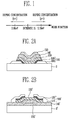
- FIG. 1 is a conceptual view illustrating change of a work function of an inorganic semiconductor according to the kind of dopant used
- FIGs. 2A and 2B are sectional views illustrating a top gate type organic thin film transistor and a bottom gate type organic thin film transistor according to a first embodiment of the present invention
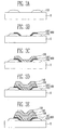
- FIGs. 3A, 3B, 3C, 3D, and3E are sectional views sequentially illustrating the manufacturing process of a top gate type organic thin film transistor according to the first embodiment of the present invention
- FIGs. 4A and 4B are sectional views illustrating a top gate type organic thin film transistor and a bottom gate type organic thin film transistor according to a second embodiment of the present invention
- FIGs. 5A, 5B, 5C, and 5D are sectional views sequentially illustrating the manufacturing process of a bottom gate type organic thin film transistor according to the second embodiment of the present invention.
- FIG. 6 is a sectional view illustrating an organic thin film transistor electrically connected to an organic light emission device.
- FIGs. 2A and 2B are schematic views illustrating a top gate type (or a staggered structured) organic thin film transistor and a bottom gate type (or an inverted staggered structured) organic thin film transistor according to a first embodiment of the present invention.
- the organic thin film transistor according to the first embodiment of the present invention includes an electrode layer 110 (or 110'), source and drain electrodes 100 (or 100') made of an impurity doping inorganic layer (or one ore more doping inorganic layers) 120 (or 120') formed at an outer side of the electrode layer 110 (or 110'), an organic semiconductor layer 130 (or 130'), a gate insulator layer 140 (or 140'), and a gate electrode 150 (or 150').
- the source and drain electrodes 100 (or 100') of the organic thin film transistor include an ohmic contact layer made of the impurity doping inorganic layer 120 (or 120') contacting the organic semiconductor layer 130 (or 130').
- the inorganic layer 120 may be fabricated in various shapes and thicknesses according to the type of the organic transistor being used, and, in one embodiment, the inorganic layer 120 (or 120') is made of silicon. However, embodiments of the present invention are not thereby limited; for example, the inorganic layer 120 (or 120') may be fabricated of compounds containing silicon and/or may be a germanium semiconductor.
- impurities are doped to adjust a work function.
- the inorganic layer 120 (or 120') is doped with antimony (Sb), arsenic (As), and/or phosphorus (P)
- the organic semiconductor layer 130 (or 130') is a P-type layer
- the inorganic layer 120 (or 120') is doped with boron (B), gallium (Ga), and/or indium (In).
- the organic semiconductor layer 130 can be used to form p- or n-type transistors.
- pentacene, and poly-3-hexylthiophene fluorene-bithiophene are used as a p-type organic semiconductor, and lutetium bisphthalocyanine, thulium bisphthalocyanine, tetracyanoquinodimethane (TCVQ), C60, C70, 1, 4, 5, 8-naphthalene tetracarboxylic dianhydride (NTCDA), 1, 4, 5, 8-naphthanlene tetracarboxylic diimide (NTCDI), 11, 11, 12, 12-tetracyanonaphtho-2, 6-quinodimethane (TCNNQ), NTCDI-C8H, NTCDI-C12H, NTCDI-C18H, NTCDI-BnCF3, and NTCDI-C8F are used as an N-type
- the gate insulator layer 140 is a layer for insulating the organic semiconductor layer 130 (or 130') and the gate electrode 150 (or (150') and may be formed by inorganic or organic materials.
- the gate electrode 150 (or 150') is formed as a top gate type electrode 150 when the transistor has a staggered structure, and as a bottom gate type electrode 150' when the transistor has an inverted staggered structure.
- the source and drain electrodes 100 are spaced apart from each other on a substrate S, the organic semiconductor layer 130 is provided on at least one region of the source and drain electrodes 100, the gate insulator layer 140 is formed on the organic semiconductor layer 130, and the gate electrode 150 is formed on the gate insulator layer 140.
- the gate electrode 150' is provided on a region of a substrate S'
- the gate insulator layer 140' is provided on the gate electrode 150' and the substrate S'
- the organic semiconductor layer 130' is provided at a position on a region of the gate insulator layer 140' corresponding to the organic semiconductor layer 130'
- at least a part of the source and drain electrodes 100' is provided on the organic semiconductor layer 130'.
- FIG. 1 is a conceptual view illustrating change of a work function of an inorganic semiconductor according to the kind of dopant used.
- an inorganic layer e.g., 120 or 120'
- the above-described condition can be satisfied by doping the silicon with a dopant density at more than 10 18 /cm 3 when the work function of the p-type semiconductor is 5.1 eV.
- the inorganic layer contacting the source and drain electrodes is formed by pentacene and the inorganic layer forming the outer sides of the source and drain electrodes is formed by silicon, then the inorganic layer may be doped with boron at a dopant density of 10 19 /cm 3 .
- an inorganic layer e.g., 120 or 120'
- the ohmic contact can be formed without doping, but doping is still performed in one embodiment of the invention to adjust the work function.
- organic thin film transistor having the staggered structure and the inverted staggered structure according to embodiments of the present invention has been described above with reference to FIGs. 2A and 2B, it should be understood by those skilled in the art that the organic thin film transistor of embodiments of the present invention may be applied to the above-described staggered structure, the above-described inverted staggered structure, an inverted coplanar structure, and/or an coplanar structure.
- FIGs. 3A to 3E a manufacturing method of the organic thin film transistor having the staggered structure containing electrodes (or layers) according to the first embodiment of the present invention will be described with reference to FIGs. 3A to 3E.
- the electrodes of the first embodiment of the present invention can easily be applied to other type transistors.
- the manufacturing method includes a source and drain electrode forming step, an organic semiconductor layer forming step, an insulator layer forming step, and a gate electrode forming step.
- the source and drain electrode forming step includes: forming the electrode layer 110 on a substrate S with metal or ITO in a pattern (which may be predetermined) and doping impurities after forming the inorganic layer 120 on the electrode layer 110.
- the organic semiconductor layer forming step includes forming the organic semiconductor layer 130 on and between the electrodes 100 with organic semiconductors.
- the insulator layer forming step includes forming the gate insulator layer 140 on the organic semiconductor layer 130, and the gate electrode forming step includes forming the gate electrode 150 on the insulator layer 140.
- a metal layer or an ITO layer is formed on the substrate S by sputtering, vapor-deposition, and/or plating, and is then patterned by etching and/or lift-off method so that the electrode layer 110 can be formed (see FIG. 3A).
- the doping of impurities after forming the inorganic layer 120 on the electrode layer 110 includes a process of forming the ohmic contact layer as the inorganic layer 120 doped with impurities on the electrode layer 110 to enable the ohmic contact between the electrodes 100 and the organic semiconductor layer 130 (see FIG. 3B).
- the inorganic layer 120 may be formed by various vapor-deposition methods such as CVD, and any unnecessary part thereof may be removed by photolithography, but embodiments of the present invention are not limited to this.
- the doping of impurities includes a process of injecting impurities into the inorganic layer 120 to change the work function of the inorganic layer 120,
- the amount and kind of the impurities injected into the ohmic contact layer are determined to satisfy the ohmic contact condition according to the work function formed by the organic semiconductor.
- the organic semiconductor layer 130 is an n-type organic semiconductor layer, then in order to form the ohmic contact of the electrodes, the n-type organic semiconductor layer (and/or inorganic semiconductor layer) is doped such that the work function of the inorganic layer 120 is less than the work function of the organic semiconductor layer 130.
- the organic semiconductor layer 130 is a p-type organic semiconductor layer
- the p-type organic semiconductor layer (and/or inorganic semiconductor layer) is doped such that the work function of the inorganic layer 120 is greater than the work function of the organic semiconductor layer 130.
- Antimony (Sb), arsenic (As), or phosphorus (P), boron (B), gallium (Ga), or indium (In) may be used as the impurities, and ion implantation and/or thermal diffusion may be used as the injection method.
- the organic semiconductor layer forming step is a step of forming the organic semiconductor layer 130 on a region of the ohmic contact layer and the substrate, and the organic semiconductor layer 130 is formed by the above-described n-type or p-type organic semiconductor.
- the organic semiconductor layer 130 may be formed by known coating method and/or printing method (see FIG. 3C).
- the insulator layer forming step is a step of forming the insulator layer 140 for insulating the gate electrode 150 to be laminated on the upper side of the organic semiconductor layer 130, and coating method and/or printing method may be used to form the insulator layer as an organic insulator layer. Alternatively, thermal diffusion, CVD, and/or SOG may be used to form the insulator layer as an inorganic insulator layer (see FIG. 3D).
- the gate electrode forming step is a step of forming the gate electrode 150 by patterning a gate metal on the gate insulator layer. This can be achieved by forming a metal layer on whole surface of the insulator layer, coating a resist layer, etching unnecessary part, and finally removing the resist layer.
- the gate electrode forming step of embodiments of the present invention is not limited to these methods (see FIG. 3E).
- electrodes (or layers) of the organic semiconductor device can be formed with impurities doped inorganic materials.
- the second embodiment uses the impurities doped inorganic material as an electrode because the impurities doped inorganic material is conductive and is directly connected to metal wires.
- FIGs. 4A and 4B are schematic structural views illustrating an organic thin film transistor of a staggered structure and an organic thin film transistor of an inverted staggered structure according to a second embodiment of the present invention.
- the organic thin film transistor is substantially the same as the organic thin film transistor employing the electrodes according to the first embodiment including the source/drain electrodes 200 (or 200'), an organic semiconductor layer 210 (or 210'), a gate insulator layer 220 (or 220'), and a gate electrode 230 (or 230').
- the organic thin film transistor of FIGs. 4A and 4B is different from the organic thin film transistor of FIGs. 2A and 2B in that the source and drain electrodes 200 (or 200') are formed by impurities doped-inorganic materials and contact the organic semiconductor layer 210 (or 210').
- the source and drain electrodes 200 or 200'
- the source and drain electrodes 200 are formed by impurities doped-inorganic materials and contact the organic semiconductor layer 210 (or 210').
- each of the source and drain electrodes 200 (or 200') of the organic thin film transistor is formed by the impurities-doped inorganic material.
- the inorganic material is silicon, but embodiments of the present invention are not limited to this; e.g., a semiconductor containing silicon and germanium may be used.
- the impurities may be antimony (Sb), arsenic (As), and/or phosphorus (P) when the organic semiconductor layer 210 is an n-type layer, and may be boron (B), gallium (Ga), and/or indium (In) when the organic semiconductor layer is a p-type layer.
- an inorganic material is doped to have a work function higher than a work function of the p-type organic semiconductor layer.
- silicon when silicon is used as the inorganic material (or p-type semiconductor), the above-described condition can be satisfied by doping the silicon with a dopant density at more than 10 18 /cm 3 when the work function of the p-type semiconductor is 5.1 eV.
- the inorganic material forming the source and drain electrodes may be doped with boron at a dopant density of 10 19 /cm 3 .
- a transistor having an n-type organic semiconductor layer e.g., 210 or 210'
- an inorganic material is doped to have a work function lower than a work function of the n-type organic semiconductor layer.
- the ohmic contact can be formed without doping, but doping is still performed in one embodiment of the invention to adjust the work function.
- organic thin film transistor having the staggered structure and the inverted staggered structure according to embodiments of the present invention has been described above, it should be understood by those skilled in the art that the organic thin film transistor of embodiments of the present invention may be applied to the above-described staggered structure, the above-described inverted staggered structure, an inverted coplanar structure, and an coplanar structure.
- FIGs. 5A to 5D a manufacturing method of the organic thin film transistor having the bottom gate type inverted staggered structure containing electrodes (or layers) according to the second embodiment of the present invention will be described with reference to FIGs. 5A to 5D.
- the electrodes of the second embodiment of the present invention can easily be applied to other type transistors.
- FIGs. 5A to 5D are sectional views sequentially illustrating the manufacturing process of an organic thin film transistor having the inverted staggered structure according to the second embodiment of the present invention, and as shown in FIGs. 5A to 5D, the manufacturing process includes a gate electrode forming step, an insulator layer forming step, an organic semiconductor layer forming step, and an electrode forming step.
- the manufacturing process includes a gate electrode forming step for forming a gate electrode on a substrate, an insulator layer forming step, an organic semiconductor layer forming step of forming an organic semiconductor layer on the insulator layer, and an electrode forming step of doping impurities on the organic semiconductor layer.
- a gate electrode forming step for forming a gate electrode on a substrate
- an insulator layer forming step for forming a gate electrode on a substrate
- an organic semiconductor layer forming step of forming an organic semiconductor layer on the insulator layer and an electrode forming step of doping impurities on the organic semiconductor layer.
- an electrode forming step will be described in more detail, while the other steps will be described briefly.
- the gate electrode forming step is a step of forming the gate electrode 230' on the substrate S' by etching, a lift-off method, etc. (see FIG. 5A)
- the insulator layer forming step is a step for forming the insulator layer 220' on the gate electrode and the substrate to insulate the gate electrode 220' (see FIG. 5B)
- the organic semiconductor layer forming step is a step of forming the organic semiconductor layer 210' formed by an organic semiconductor for connecting the source electrode to the drain electrode using a coating method and/or a printing method (see FIG. 5C).
- the electrode forming step is a step of forming the source and drain electrodes 200' formed on the top of the organic semiconductor layer 210' with the impurities-doped materials.
- the electrodes 200' may be formed by forming an electrode layer with an inorganic semiconductor and injecting ions into the electrode layer to form the impurities doped inorganic electrodes 200', or the electrodes 200' may be formed by depositing gas containing impurity such as a silane (SiH 4 ) (see FIG. 5D).
- the n-type organic semiconductor layer (and/or the inorganic semiconductor layer) is doped such that the inorganic material (or the inorganic material of the inorganic electrodes 200') has a work function less than a work function of the organic semiconductor layer 210'.
- the p-type organic semiconductor layer (and/or the inorganic semiconductor layer) is doped such that the inorganic material (or the inorganic material of the inorganic electrodes 200') has a work function higher than a work function of the organic semiconductor layer 210.
- the impurities antimony (Sb), arsenic (As), phosphorus (P), boron (B), gallium (Ga), and indium (In) may be used.
- ions may be injected by ion implantation and/or thermal diffusion.
- the flat panel display device includes a display region having a light emission device and a driving part including the one or more organic thin film transistors electrically connected to the light emission device.
- the organic thin film transistor may be applied to any flat panel display device, and, in one embodiment, may be applied to an organic light emission display device.
- FIG. 6 illustrates a coplanar structured organic thin film transistor electrically connected to an organic light emission device of a flat panel display device.
- the organic semiconductor layer 330 is provided on a region of a substrate
- a gate insulator layer 335 is provided on organic semiconductor layer 330
- a gate electrode 320 is formed at a position of a region of the gate insulator layer 335 corresponding to the organic semiconductor layer 330
- an interlayer insulator layer 380 is further formed on the gate electrode 320
- the source and drain electrodes 310 are formed on the interlayer insulator layer 380 and contacts the organic semiconductor layer 330 through one or more contact holes formed to expose a region (or regions) of the organic semiconductor layer 330, wherein the region may be predetermined.
- the source and drain electrodes 310 are formed by an inorganic material doped with impurities and electrically connected to a first electrode 350 of the organic light emission device to drive the organic light emission device.
Landscapes
- Engineering & Computer Science (AREA)
- Manufacturing & Machinery (AREA)
- Thin Film Transistor (AREA)
Abstract
Description
- The present invention relates to an organic thin film transistor and a flat panel display device using the same, and more particularly, to an organic thin film transistor formed between source and drain electrodes and an organic semiconductor and a flat panel display device using the same.
- When fabricating an organic semiconductor device, an energy barrier between an organic semiconductor and a metal should be removed by forming an ohmic contact between the organic semiconductor and the metal. In a conventional organic semiconductor device, pentacene, and poly-3-hexylthiophene, fluorene-bithiophene are used as a p-type organic semiconductor, and lutetium bisphthalocyanine, thulium bisphthalocyanine, tetracyanoquinodimethane (TCVQ), C60, C70, 1, 4, 5, 8-naphthalene tetracarboxylic dianhydride (NTCDA), 1, 4, 5, 8-naphthanlene tetracarboxylic diimide (NTCDI), 11, 11, 12, 12-tetracyanonaphtho-2, 6-quinodimethane (TCNNQ), NTCDI-C8H, NTCDI-C12H, NTCDI-C18H, NTCDI-BnCF3, and NTCDI-C8F are used as an N-type organic semiconductor.
- Since the organic transistor materials have high work functions ranging from 5.1 eV to 5.5 eV, the ohmic contact is formed using gold (Au) satisfying the high work functions or surface-treated indium-tin oxide (ITO). However, since a shadow mask type patterning is required when using gold as the ohmic contact, gaps between channels are limited by the mask edges; and, when ITO is used as the ohmic contact, the lifespan and the stability of the device deteriorate.
- Accordingly, it is an aspect of the present invention to provide an organic thin film transistor in which an ohmic contact is formed between source and drain electrodes and an organic semiconductor layer of an organic thin film transistor and a flat panel display device using the same.
- In an embodiment of the present invention, an organic thin film transistor includes: a gate electrode; a gate insulator layer insulating the gate electrode; an organic semiconductor layer contacting the gate insulator layer; source and drain electrodes contacting the organic semiconductor layer; and an inorganic layer on at least one region of the source and drain electrodes, wherein the inorganic layer is doped with an impurity.
- In another embodiment of the present invention, an organic thin film transistor includes: a gate electrode; a gate insulator layer insulating the gate electrode; an organic semiconductor layer contacting the gate insulator layer; and source and drain electrodes contacting the organic semiconductor layer, the source and drain electrodes including an inorganic material doped with an impurity.
- According to an aspect of the present invention, there is provided an organic thin film transistor as set out in Claim 1. Preferred features of this aspect are set out in Claims 2 to 14.
- According to another aspect of the invention, there is provided a flat panel display device as set out in Claim 15. Preferred features of this aspect are set out in
- According to another aspect of the invention, there is provided a method of manufacturing an organic thin film transistor as set out in Claim 19. Preferred features of this aspect are set out in Claim 20.
- As such, in an organic thin film transistor in accordance with one embodiment of the present invention, the organic thin film transistor includes source and drain electrodes and an organic semiconductor layer. In this embodiment, an ohmic contact is formed between the source and drain electrodes and the organic semiconductor layer so that emission efficiency and stability are enhanced. In addition, by simply adjusting a doping concentration of impurities constituting an inorganic layer or the source and drain electrodes, this embodiment of the present invention allows the ohmic contact condition to change according to the kind of the organic semiconductor layer implemented.
- The accompanying drawings, together with the specification, illustrate exemplary embodiments of the present invention, and, together with the description, serve to explain the principles of the present invention.
- FIG. 1 is a conceptual view illustrating change of a work function of an inorganic semiconductor according to the kind of dopant used;
- FIGs. 2A and 2B are sectional views illustrating a top gate type organic thin film transistor and a bottom gate type organic thin film transistor according to a first embodiment of the present invention;
- FIGs. 3A, 3B, 3C, 3D, and3E are sectional views sequentially illustrating the manufacturing process of a top gate type organic thin film transistor according to the first embodiment of the present invention;
- FIGs. 4A and 4B are sectional views illustrating a top gate type organic thin film transistor and a bottom gate type organic thin film transistor according to a second embodiment of the present invention;
- FIGs. 5A, 5B, 5C, and 5D are sectional views sequentially illustrating the manufacturing process of a bottom gate type organic thin film transistor according to the second embodiment of the present invention; and
- FIG. 6 is a sectional view illustrating an organic thin film transistor electrically connected to an organic light emission device.
- In the following detailed description, certain exemplary embodiments of the present invention are shown and described, by way of illustration. As those skilled in the art would recognize, the described exemplary embodiments may be modified in various ways, all without departing from the scope of the present invention. Accordingly, the drawings and description are to be regarded as illustrative in nature, rather than restrictive.
- FIGs. 2A and 2B are schematic views illustrating a top gate type (or a staggered structured) organic thin film transistor and a bottom gate type (or an inverted staggered structured) organic thin film transistor according to a first embodiment of the present invention. The organic thin film transistor according to the first embodiment of the present invention includes an electrode layer 110 (or 110'), source and drain electrodes 100 (or 100') made of an impurity doping inorganic layer (or one ore more doping inorganic layers) 120 (or 120') formed at an outer side of the electrode layer 110 (or 110'), an organic semiconductor layer 130 (or 130'), a gate insulator layer 140 (or 140'), and a gate electrode 150 (or 150').
- The source and drain electrodes 100 (or 100') of the organic thin film transistor include an ohmic contact layer made of the impurity doping inorganic layer 120 (or 120') contacting the organic semiconductor layer 130 (or 130').
- The inorganic layer 120 (or 120') may be fabricated in various shapes and thicknesses according to the type of the organic transistor being used, and, in one embodiment, the inorganic layer 120 (or 120') is made of silicon. However, embodiments of the present invention are not thereby limited; for example, the inorganic layer 120 (or 120') may be fabricated of compounds containing silicon and/or may be a germanium semiconductor.
- In the inorganic layer 120 (or 120'), impurities are doped to adjust a work function. For example, when the organic semiconductor layer 130 (or 130') is an n-type layer, the inorganic layer 120 (or 120') is doped with antimony (Sb), arsenic (As), and/or phosphorus (P), and when the organic semiconductor layer 130 (or 130') is a P-type layer, the inorganic layer 120 (or 120') is doped with boron (B), gallium (Ga), and/or indium (In).
- The organic semiconductor layer 130 (or 130') can be used to form p- or n-type transistors. In the organic semiconductor layer 130 (or 130'), pentacene, and poly-3-hexylthiophene, fluorene-bithiophene are used as a p-type organic semiconductor, and lutetium bisphthalocyanine, thulium bisphthalocyanine, tetracyanoquinodimethane (TCVQ), C60, C70, 1, 4, 5, 8-naphthalene tetracarboxylic dianhydride (NTCDA), 1, 4, 5, 8-naphthanlene tetracarboxylic diimide (NTCDI), 11, 11, 12, 12-tetracyanonaphtho-2, 6-quinodimethane (TCNNQ), NTCDI-C8H, NTCDI-C12H, NTCDI-C18H, NTCDI-BnCF3, and NTCDI-C8F are used as an N-type organic semiconductor.
- The gate insulator layer 140 (or 140') is a layer for insulating the organic semiconductor layer 130 (or 130') and the gate electrode 150 (or (150') and may be formed by inorganic or organic materials.
- The gate electrode 150 (or 150') is formed as a top
gate type electrode 150 when the transistor has a staggered structure, and as a bottom gate type electrode 150' when the transistor has an inverted staggered structure. - In other words, in the staggered structure as shown in FIG. 2A, the source and
drain electrodes 100 are spaced apart from each other on a substrate S, theorganic semiconductor layer 130 is provided on at least one region of the source anddrain electrodes 100, thegate insulator layer 140 is formed on theorganic semiconductor layer 130, and thegate electrode 150 is formed on thegate insulator layer 140. - By contrast, in the inverted staggered structure of FIG. 2B, the gate electrode 150' is provided on a region of a substrate S', the gate insulator layer 140' is provided on the gate electrode 150' and the substrate S', the organic semiconductor layer 130' is provided at a position on a region of the gate insulator layer 140' corresponding to the organic semiconductor layer 130', and at least a part of the source and drain electrodes 100' is provided on the organic semiconductor layer 130'.
- FIG. 1 is a conceptual view illustrating change of a work function of an inorganic semiconductor according to the kind of dopant used.
- In a transistor having a p-type organic semiconductor layer (e.g., 130 or 130') according to the first embodiment, an inorganic layer (e.g., 120 or 120') is doped to have a work function higher than a work function of the p-type organic semiconductor layer. In this case, referring also to FIG. 1, when silicon is used as the inorganic layer (or p-type semiconductor), the above-described condition can be satisfied by doping the silicon with a dopant density at more than 1018/cm3 when the work function of the p-type semiconductor is 5.1 eV. For example, if the organic semiconductor layer contacting the source and drain electrodes is formed by pentacene and the inorganic layer forming the outer sides of the source and drain electrodes is formed by silicon, then the inorganic layer may be doped with boron at a dopant density of 1019/cm3.
- By contrast, in a transistor having an n-type organic semiconductor layer (e.g., 130 or 130') according to the first embodiment of the present invention, an inorganic layer (e.g., 120 or 120') is doped to have a work function lower than a work function of the n-type organic semiconductor layer. However, in this transistor (or the n-type organic transistor), the ohmic contact can be formed without doping, but doping is still performed in one embodiment of the invention to adjust the work function.
- Also, although the organic thin film transistor having the staggered structure and the inverted staggered structure according to embodiments of the present invention has been described above with reference to FIGs. 2A and 2B, it should be understood by those skilled in the art that the organic thin film transistor of embodiments of the present invention may be applied to the above-described staggered structure, the above-described inverted staggered structure, an inverted coplanar structure, and/or an coplanar structure.
- Hereinafter, a manufacturing method of the organic thin film transistor having the staggered structure containing electrodes (or layers) according to the first embodiment of the present invention will be described with reference to FIGs. 3A to 3E. Through this description, it should be understood by those skilled in the art that the electrodes of the first embodiment of the present invention can easily be applied to other type transistors.
- The manufacturing method includes a source and drain electrode forming step, an organic semiconductor layer forming step, an insulator layer forming step, and a gate electrode forming step. The source and drain electrode forming step includes: forming the
electrode layer 110 on a substrate S with metal or ITO in a pattern (which may be predetermined) and doping impurities after forming theinorganic layer 120 on theelectrode layer 110. The organic semiconductor layer forming step includes forming theorganic semiconductor layer 130 on and between theelectrodes 100 with organic semiconductors. The insulator layer forming step includes forming thegate insulator layer 140 on theorganic semiconductor layer 130, and the gate electrode forming step includes forming thegate electrode 150 on theinsulator layer 140. - In the forming of the
electrode layer 110 on the substrate S with metal or ITO, a metal layer or an ITO layer is formed on the substrate S by sputtering, vapor-deposition, and/or plating, and is then patterned by etching and/or lift-off method so that theelectrode layer 110 can be formed (see FIG. 3A). - The doping of impurities after forming the
inorganic layer 120 on theelectrode layer 110 includes a process of forming the ohmic contact layer as theinorganic layer 120 doped with impurities on theelectrode layer 110 to enable the ohmic contact between theelectrodes 100 and the organic semiconductor layer 130 (see FIG. 3B). - For example, it should be apparent to those skilled in the art that the
inorganic layer 120 may be formed by various vapor-deposition methods such as CVD, and any unnecessary part thereof may be removed by photolithography, but embodiments of the present invention are not limited to this. - Also, the doping of impurities includes a process of injecting impurities into the
inorganic layer 120 to change the work function of theinorganic layer 120, The amount and kind of the impurities injected into the ohmic contact layer are determined to satisfy the ohmic contact condition according to the work function formed by the organic semiconductor. In other words, as described above, if theorganic semiconductor layer 130 is an n-type organic semiconductor layer, then in order to form the ohmic contact of the electrodes, the n-type organic semiconductor layer (and/or inorganic semiconductor layer) is doped such that the work function of theinorganic layer 120 is less than the work function of theorganic semiconductor layer 130. By contrast, if theorganic semiconductor layer 130 is a p-type organic semiconductor layer, then in order to form the ohmic contact of the electrodes, the p-type organic semiconductor layer (and/or inorganic semiconductor layer) is doped such that the work function of theinorganic layer 120 is greater than the work function of theorganic semiconductor layer 130. Antimony (Sb), arsenic (As), or phosphorus (P), boron (B), gallium (Ga), or indium (In) may be used as the impurities, and ion implantation and/or thermal diffusion may be used as the injection method. - The organic semiconductor layer forming step is a step of forming the
organic semiconductor layer 130 on a region of the ohmic contact layer and the substrate, and theorganic semiconductor layer 130 is formed by the above-described n-type or p-type organic semiconductor. Theorganic semiconductor layer 130 may be formed by known coating method and/or printing method (see FIG. 3C). - The insulator layer forming step is a step of forming the
insulator layer 140 for insulating thegate electrode 150 to be laminated on the upper side of theorganic semiconductor layer 130, and coating method and/or printing method may be used to form the insulator layer as an organic insulator layer. Alternatively, thermal diffusion, CVD, and/or SOG may be used to form the insulator layer as an inorganic insulator layer (see FIG. 3D). - The gate electrode forming step is a step of forming the
gate electrode 150 by patterning a gate metal on the gate insulator layer. This can be achieved by forming a metal layer on whole surface of the insulator layer, coating a resist layer, etching unnecessary part, and finally removing the resist layer. However, the gate electrode forming step of embodiments of the present invention is not limited to these methods (see FIG. 3E). - By contrast, in a second embodiment of the present invention, electrodes (or layers) of the organic semiconductor device can be formed with impurities doped inorganic materials. In other words, instead of forming the ohmic contact layer on the metal electrode layer as is in the first embodiment, the second embodiment uses the impurities doped inorganic material as an electrode because the impurities doped inorganic material is conductive and is directly connected to metal wires.
- FIGs. 4A and 4B are schematic structural views illustrating an organic thin film transistor of a staggered structure and an organic thin film transistor of an inverted staggered structure according to a second embodiment of the present invention.
- As shown in FIGs. 4A and 4B, the organic thin film transistor is substantially the same as the organic thin film transistor employing the electrodes according to the first embodiment including the source/drain electrodes 200 (or 200'), an organic semiconductor layer 210 (or 210'), a gate insulator layer 220 (or 220'), and a gate electrode 230 (or 230'). However, the organic thin film transistor of FIGs. 4A and 4B is different from the organic thin film transistor of FIGs. 2A and 2B in that the source and drain electrodes 200 (or 200') are formed by impurities doped-inorganic materials and contact the organic semiconductor layer 210 (or 210'). Thus, a detailed description of general components of the organic thin film transistor except for the source and drain
electrodes 200 will be omitted. - As shown, each of the source and drain electrodes 200 (or 200') of the organic thin film transistor is formed by the impurities-doped inorganic material. In one embodiment, the inorganic material is silicon, but embodiments of the present invention are not limited to this; e.g., a semiconductor containing silicon and germanium may be used. The impurities may be antimony (Sb), arsenic (As), and/or phosphorus (P) when the
organic semiconductor layer 210 is an n-type layer, and may be boron (B), gallium (Ga), and/or indium (In) when the organic semiconductor layer is a p-type layer. - In a transistor having a p-type organic semiconductor layer (e.g., 210 or 210') according to the second embodiment, an inorganic material is doped to have a work function higher than a work function of the p-type organic semiconductor layer. In this case and referring also to FIG. 1, when silicon is used as the inorganic material (or p-type semiconductor), the above-described condition can be satisfied by doping the silicon with a dopant density at more than 1018/cm3 when the work function of the p-type semiconductor is 5.1 eV. For example, if the organic semiconductor layer contacting the source and drain electrodes is formed by pentacene and the inorganic material forming the source and drain electrodes is formed by silicon, then the inorganic material may be doped with boron at a dopant density of 1019/cm3.
- By contrast, in a transistor having an n-type organic semiconductor layer (e.g., 210 or 210') according to the second embodiment of the present invention, an inorganic material is doped to have a work function lower than a work function of the n-type organic semiconductor layer. However, in this transistor (or the n-type organic transistor), the ohmic contact can be formed without doping, but doping is still performed in one embodiment of the invention to adjust the work function.
- Also, although the organic thin film transistor having the staggered structure and the inverted staggered structure according to embodiments of the present invention has been described above, it should be understood by those skilled in the art that the organic thin film transistor of embodiments of the present invention may be applied to the above-described staggered structure, the above-described inverted staggered structure, an inverted coplanar structure, and an coplanar structure.
- Hereinafter, a manufacturing method of the organic thin film transistor having the bottom gate type inverted staggered structure containing electrodes (or layers) according to the second embodiment of the present invention will be described with reference to FIGs. 5A to 5D. Through this description, it should be understood by those skilled in the art that the electrodes of the second embodiment of the present invention can easily be applied to other type transistors.
- FIGs. 5A to 5D are sectional views sequentially illustrating the manufacturing process of an organic thin film transistor having the inverted staggered structure according to the second embodiment of the present invention, and as shown in FIGs. 5A to 5D, the manufacturing process includes a gate electrode forming step, an insulator layer forming step, an organic semiconductor layer forming step, and an electrode forming step.
- The manufacturing process includes a gate electrode forming step for forming a gate electrode on a substrate, an insulator layer forming step, an organic semiconductor layer forming step of forming an organic semiconductor layer on the insulator layer, and an electrode forming step of doping impurities on the organic semiconductor layer. For description clarity, the electrode forming step will be described in more detail, while the other steps will be described briefly.
- The gate electrode forming step is a step of forming the gate electrode 230' on the substrate S' by etching, a lift-off method, etc. (see FIG. 5A), the insulator layer forming step is a step for forming the insulator layer 220' on the gate electrode and the substrate to insulate the gate electrode 220' (see FIG. 5B), and the organic semiconductor layer forming step is a step of forming the organic semiconductor layer 210' formed by an organic semiconductor for connecting the source electrode to the drain electrode using a coating method and/or a printing method (see FIG. 5C).
- The electrode forming step is a step of forming the source and drain electrodes 200' formed on the top of the organic semiconductor layer 210' with the impurities-doped materials. Here, the electrodes 200' may be formed by forming an electrode layer with an inorganic semiconductor and injecting ions into the electrode layer to form the impurities doped inorganic electrodes 200', or the electrodes 200' may be formed by depositing gas containing impurity such as a silane (SiH4) (see FIG. 5D).
- In addition, if the impurities are injected, in a case when the organic semiconductor layer 210' is an n-type organic semiconductor layer, then in order to form the ohmic contact of the electrodes, the n-type organic semiconductor layer (and/or the inorganic semiconductor layer) is doped such that the inorganic material (or the inorganic material of the inorganic electrodes 200') has a work function less than a work function of the organic semiconductor layer 210'. Moreover, in a case when the organic semiconductor layer 210' is a p-type organic semiconductor layer, in order to form the ohmic contact of the electrodes, the p-type organic semiconductor layer (and/or the inorganic semiconductor layer) is doped such that the inorganic material (or the inorganic material of the inorganic electrodes 200') has a work function higher than a work function of the
organic semiconductor layer 210. As the impurities, antimony (Sb), arsenic (As), phosphorus (P), boron (B), gallium (Ga), and indium (In) may be used. Moreover, ions may be injected by ion implantation and/or thermal diffusion. - Next, a flat panel display device using one or more organic thin film transistors as described above will be described. The flat panel display device according to one embodiment of the present invention includes a display region having a light emission device and a driving part including the one or more organic thin film transistors electrically connected to the light emission device. Those skilled in the art should understand that the organic thin film transistor may be applied to any flat panel display device, and, in one embodiment, may be applied to an organic light emission display device.
- FIG. 6 illustrates a coplanar structured organic thin film transistor electrically connected to an organic light emission device of a flat panel display device. As shown in the drawing, the
organic semiconductor layer 330 is provided on a region of a substrate, a gate insulator layer 335 is provided onorganic semiconductor layer 330, agate electrode 320 is formed at a position of a region of the gate insulator layer 335 corresponding to theorganic semiconductor layer 330, an interlayer insulator layer 380 is further formed on thegate electrode 320, and the source and drainelectrodes 310 are formed on the interlayer insulator layer 380 and contacts theorganic semiconductor layer 330 through one or more contact holes formed to expose a region (or regions) of theorganic semiconductor layer 330, wherein the region may be predetermined. - The source and drain
electrodes 310 are formed by an inorganic material doped with impurities and electrically connected to afirst electrode 350 of the organic light emission device to drive the organic light emission device. - Although certain embodiments of the present invention have been shown and described, it would be appreciated by those skilled in the art that changes might be made in these embodiments without departing from the principles of the invention, the scope of which is defined in the claims and their equivalents. For example, those skilled in the art should understand that the shape and the material of the inorganic layer and the kinds of the organic thin film transistor employed in the present invention may be modified.
Claims (20)
- An organic thin film transistor comprising:a gate electrode;a gate insulator layer arranged to insulate the gate electrode;an organic semiconductor layer contacting the gate insulator layer; andsource and drain electrodes contacting the organic semiconductor layer, at least one of the source and drain electrodes including an inorganic material doped with an impurity.
- An organic thin film transistor according to claim 1, wherein:the inorganic material comprises an inorganic layer formed on at least one region of the organic semiconductor layer.
- An organic thin film transistor according to claim 2, wherein said at least one of the source and drain electrodes further comprises a conductive electrode layer arranged to contact the inorganic layer.
- An organic thin film transistor according to any one of claims 1 to 3,
wherein the inorganic material includes at least one of silicon, compounds containing silicon, or germanium. - An organic thin film transistor according to claim 1 or 4, wherein the organic semiconductor layer contacting the source and drain electrodes is an n-type semiconductor, and wherein a work function of the source and drain electrodes is less than a work function of the organic semiconductor layer.
- An organic thin film transistor according to any one of claims 2 to 4,
wherein the organic semiconductor layer contacting the source and drain electrodes is an n-type semiconductor, and wherein a work function of the inorganic layer doped with the impurity is less than a work function of the organic semiconductor layer. - An organic thin film transistor according to claim 5 or 6, wherein the impurity includes at least one of antimony (Sb), arsenic (As), or phosphorus (P).
- An organic thin film transistor according to claim 1 or 4, wherein the organic semiconductor layer contacting the source and drain electrodes is a p-type semiconductor, and wherein a work function of the source and drain electrodes is higher than a work function of the organic semiconductor layer.
- An organic thin film transistor according to any one of claims 2 to 4,
wherein the organic semiconductor layer contacting the source and drain electrodes is a p-type semiconductor, and wherein a work function of the inorganic layer doped with the impurity is higher than a work function of the organic semiconductor layer. - A organic thin film transistor according to claim 8 or 9, wherein the impurity includes at least one of boron (B), gallium (Ga), or indium (In).
- An organic thin film transistor according to any preceding claim,
wherein the organic semiconductor layer contacting the source and drain electrodes is pentacene, and wherein the inorganic material of the source and drain electrodes is silicon doped with boron. - An organic thin film transistor according to any preceding claim,
wherein the source and drain electrodes are provided on a substrate and spaced apart from each other, wherein the organic semiconductor layer is formed on one region of the source and drain electrodes and the substrate, wherein the gate insulator layer is formed on the organic semiconductor layer, and wherein the gate electrode is formed on the gate insulator layer. - An organic thin film transistor according to any one of claims 1 to 11,
wherein the gate electrode is formed on one region of a substrate, wherein the gate insulator layer is formed on the gate electrode and the substrate, wherein the organic semiconductor layer is formed on the gate electrode insulator layer, and at least a part of the source and drain electrodes is formed on the organic semiconductor layer. - An organic thin film transistor according to any one of claims 1 to 11,
wherein the organic semiconductor layer is formed on one region of the substrate,
wherein the gate insulator layer is formed on the organic semiconductor layer, wherein the gate electrode is formed on one region of the gate insulator layer corresponding to the organic semiconductor layer, wherein an interlayer insulator layer is further formed on the gate electrode, and the source and drain electrodes are formed on the interlayer insulator layer and contact the organic semiconductor layer through a contact hole formed to expose a region of the organic semiconductor layer. - A flat panel display device comprising:an organic thin film transistor electrically connected to a light emission device and adapted to drive the same,the organic thin film transistor including source and drain electrodes and an organic semiconductor layer contacting the source and drain electrodes, at least one of the source and drain electrodes comprising an inorganic material doped with an impurity.
- A flat panel display device according to claim 15, wherein:the inorganic material comprises an inorganic layer formed on at least one region of the organic semiconductor layer.
- A flat panel display device according to claim 15 or 16, wherein the light emission device comprises an organic light emission device.
- A flat panel display device according to any one of claims 15 or 16,
wherein the inorganic material includes at least one of silicon, compound containing silicon, or germanium. - A method of manufacturing an organic thin film transistor comprising:forming a gate electrode;providing a gate insulating layer arranged to insulate the gate electrode;forming an organic semiconductor layer so as to contact the gate insulating layer; andforming source and drain electrodes so as to contact the organic semiconductor layer, at least one of the source and drain electrodes comprising an inorganic material doped with an impurity.
- A method according to claim 19, wherein the inorganic material comprises an inorganic layer formed on at least one region of the organic semiconductor layer.
Applications Claiming Priority (1)
| Application Number | Priority Date | Filing Date | Title |
|---|---|---|---|
| KR1020050073946A KR100658286B1 (en) | 2005-08-11 | 2005-08-11 | Organic thin film transistor and flat panel display device using same |
Publications (3)
| Publication Number | Publication Date |
|---|---|
| EP1753046A2 true EP1753046A2 (en) | 2007-02-14 |
| EP1753046A3 EP1753046A3 (en) | 2011-06-15 |
| EP1753046B1 EP1753046B1 (en) | 2015-06-10 |
Family
ID=37402731
Family Applications (1)
| Application Number | Title | Priority Date | Filing Date |
|---|---|---|---|
| EP06254238.6A Not-in-force EP1753046B1 (en) | 2005-08-11 | 2006-08-11 | Organic thin film transistor and flat panel display device using the same |
Country Status (3)
| Country | Link |
|---|---|
| US (1) | US7842943B2 (en) |
| EP (1) | EP1753046B1 (en) |
| KR (1) | KR100658286B1 (en) |
Cited By (1)
| Publication number | Priority date | Publication date | Assignee | Title |
|---|---|---|---|---|
| TWI463669B (en) * | 2010-07-07 | 2014-12-01 | Sony Corp | Thin film transistor, method of manufacturing thin film transistor, display device, and electronic equipment |
Families Citing this family (1)
| Publication number | Priority date | Publication date | Assignee | Title |
|---|---|---|---|---|
| KR101137391B1 (en) * | 2010-03-24 | 2012-04-20 | 삼성모바일디스플레이주식회사 | Thin film transistor substrate, method of manufacturing the same, and organic light emitting device having the Thin film transistor substrate |
Family Cites Families (20)
| Publication number | Priority date | Publication date | Assignee | Title |
|---|---|---|---|---|
| TW232751B (en) * | 1992-10-09 | 1994-10-21 | Semiconductor Energy Res Co Ltd | Semiconductor device and method for forming the same |
| US20010048147A1 (en) * | 1995-09-14 | 2001-12-06 | Hideki Mizuhara | Semiconductor devices passivation film |
| US6337520B1 (en) * | 1997-02-26 | 2002-01-08 | Samsung Electronics Co., Ltd. | Composition for a wiring, a wiring using the composition, manufacturing method thereof, a display using the wiring and manufacturing method thereof |
| KR100739366B1 (en) * | 1999-12-20 | 2007-07-16 | 엘지.필립스 엘시디 주식회사 | Thin Film Transistor and Manufacturing Method Thereof |
| GB2371910A (en) * | 2001-01-31 | 2002-08-07 | Seiko Epson Corp | Display devices |
| US6433359B1 (en) * | 2001-09-06 | 2002-08-13 | 3M Innovative Properties Company | Surface modifying layers for organic thin film transistors |
| DE10153562A1 (en) * | 2001-10-30 | 2003-05-15 | Infineon Technologies Ag | Process for reducing the electrical contact resistance in organic field-effect transistors by embedding nanoparticles to produce field peaks at the interface between the contact material and the organic semiconductor material |
| KR100527087B1 (en) * | 2001-12-22 | 2005-11-09 | 비오이 하이디스 테크놀로지 주식회사 | Method of fabricating X-ray detector |
| JP4247377B2 (en) * | 2001-12-28 | 2009-04-02 | 独立行政法人産業技術総合研究所 | Thin film transistor and manufacturing method thereof |
| JP2003298056A (en) | 2002-03-28 | 2003-10-17 | National Institute Of Advanced Industrial & Technology | Organic thin film field effect transistor and method of manufacturing the same |
| JP2004146430A (en) | 2002-10-22 | 2004-05-20 | Konica Minolta Holdings Inc | Organic thin film transistor, organic TFT device, and method of manufacturing the same |
| JP2004103905A (en) * | 2002-09-11 | 2004-04-02 | Pioneer Electronic Corp | Organic semiconductor device |
| CN1186822C (en) * | 2002-09-23 | 2005-01-26 | 中国科学院长春应用化学研究所 | Organic film transistor and preparing method |
| EP1434281A3 (en) * | 2002-12-26 | 2007-10-24 | Konica Minolta Holdings, Inc. | Manufacturing method of thin-film transistor, thin-film transistor sheet, and electric circuit |
| JP2004235298A (en) * | 2003-01-29 | 2004-08-19 | Pioneer Electronic Corp | Organic semiconductor device and method of manufacturing the same |
| TWI238449B (en) * | 2003-06-06 | 2005-08-21 | Pioneer Corp | Organic semiconductor device and method of manufacture of same |
| JP4997688B2 (en) | 2003-08-19 | 2012-08-08 | セイコーエプソン株式会社 | Electrode, thin film transistor, electronic circuit, display device and electronic device |
| JP2005079560A (en) * | 2003-09-04 | 2005-03-24 | Hitachi Ltd | Thin film transistor, display device, and manufacturing method thereof |
| US7554121B2 (en) * | 2003-12-26 | 2009-06-30 | Semiconductor Energy Laboratory Co., Ltd. | Organic semiconductor device |
| DE102004010094B3 (en) * | 2004-02-27 | 2005-12-22 | Infineon Technologies Ag | Semiconductor device having at least one organic semiconductor layer and method for its production |
-
2005
- 2005-08-11 KR KR1020050073946A patent/KR100658286B1/en not_active Expired - Fee Related
-
2006
- 2006-08-09 US US11/501,976 patent/US7842943B2/en not_active Expired - Fee Related
- 2006-08-11 EP EP06254238.6A patent/EP1753046B1/en not_active Not-in-force
Cited By (1)
| Publication number | Priority date | Publication date | Assignee | Title |
|---|---|---|---|---|
| TWI463669B (en) * | 2010-07-07 | 2014-12-01 | Sony Corp | Thin film transistor, method of manufacturing thin film transistor, display device, and electronic equipment |
Also Published As
| Publication number | Publication date |
|---|---|
| EP1753046A3 (en) | 2011-06-15 |
| KR100658286B1 (en) | 2006-12-14 |
| US20070034867A1 (en) | 2007-02-15 |
| EP1753046B1 (en) | 2015-06-10 |
| US7842943B2 (en) | 2010-11-30 |
Similar Documents
| Publication | Publication Date | Title |
|---|---|---|
| JP5638944B2 (en) | Organic thin film transistor | |
| JP4319163B2 (en) | Nanowire light emitting device and manufacturing method thereof | |
| CN103403873B (en) | offset electrode TFT structure | |
| KR100601370B1 (en) | Thin film transistor and organic electroluminescent display using same | |
| US6617608B2 (en) | Electro-luminescent display and a method of manufacturing the same | |
| US8470624B2 (en) | Fabricating method of organic electro-luminescence display unit | |
| KR102335772B1 (en) | Electronic devices having side gate and 2D material channel and method of manufacturing the same | |
| US9899616B2 (en) | Organic field effect transistor and method for producing the same | |
| US8394665B2 (en) | Organic thin film transistors, organic light-emissive devices and organic light-emissive displays | |
| KR20140059576A (en) | Transparent thin film transistor, and organic light emitting display device therewith | |
| TWI422039B (en) | Thin film transistor element and manufacturing method thereof | |
| CN105206677A (en) | Oxide semiconductor thin film transistor and manufacturing method thereof | |
| EP2760060B1 (en) | Quasi-surface emission vertical-type organic light-emitting transistors and method of manufacturing the same | |
| KR101933771B1 (en) | Transistor having doped organic thin layer | |
| CN1542986A (en) | Thin film transistor, method of manufacturing the same, and display device using the same | |
| EP1753046B1 (en) | Organic thin film transistor and flat panel display device using the same | |
| KR100237180B1 (en) | Configuration of mos transistor | |
| CN114823722A (en) | Display panel | |
| US12324302B2 (en) | Dual plate OLET displays | |
| US7649217B2 (en) | Thin film field effect transistors having Schottky gate-channel junctions | |
| KR100659060B1 (en) | Manufacturing method of organic light emitting display device | |
| KR20240071695A (en) | Tunneling Field Effect Transistor | |
| TW202425142A (en) | Semiconductor device and forming method thereof | |
| CN117476666A (en) | LTPO substrate manufacturing method, LTPO substrate and display panel | |
| KUDO et al. | Organic Light-Emitting Transistors for Flexible Active Matrix Displays |
Legal Events
| Date | Code | Title | Description |
|---|---|---|---|
| PUAI | Public reference made under article 153(3) epc to a published international application that has entered the european phase |
Free format text: ORIGINAL CODE: 0009012 |
|
| 17P | Request for examination filed |
Effective date: 20060817 |
|
| AK | Designated contracting states |
Kind code of ref document: A2 Designated state(s): AT BE BG CH CY CZ DE DK EE ES FI FR GB GR HU IE IS IT LI LT LU LV MC NL PL PT RO SE SI SK TR |
|
| AX | Request for extension of the european patent |
Extension state: AL BA HR MK YU |
|
| RAP1 | Party data changed (applicant data changed or rights of an application transferred) |
Owner name: SAMSUNG MOBILE DISPLAY CO., LTD. |
|
| PUAL | Search report despatched |
Free format text: ORIGINAL CODE: 0009013 |
|
| AK | Designated contracting states |
Kind code of ref document: A3 Designated state(s): AT BE BG CH CY CZ DE DK EE ES FI FR GB GR HU IE IS IT LI LT LU LV MC NL PL PT RO SE SI SK TR |
|
| AX | Request for extension of the european patent |
Extension state: AL BA HR MK RS |
|
| 17Q | First examination report despatched |
Effective date: 20120118 |
|
| AKX | Designation fees paid |
Designated state(s): DE FR GB |
|
| RAP1 | Party data changed (applicant data changed or rights of an application transferred) |
Owner name: SAMSUNG DISPLAY CO., LTD. |
|
| RIC1 | Information provided on ipc code assigned before grant |
Ipc: H01L 27/32 20060101ALI20140822BHEP Ipc: H01L 51/10 20060101AFI20140822BHEP |
|
| GRAP | Despatch of communication of intention to grant a patent |
Free format text: ORIGINAL CODE: EPIDOSNIGR1 |
|
| INTG | Intention to grant announced |
Effective date: 20150105 |
|
| GRAS | Grant fee paid |
Free format text: ORIGINAL CODE: EPIDOSNIGR3 |
|
| GRAA | (expected) grant |
Free format text: ORIGINAL CODE: 0009210 |
|
| AK | Designated contracting states |
Kind code of ref document: B1 Designated state(s): DE FR GB |
|
| REG | Reference to a national code |
Ref country code: GB Ref legal event code: FG4D |
|
| REG | Reference to a national code |
Ref country code: DE Ref legal event code: R096 Ref document number: 602006045649 Country of ref document: DE |
|
| RAP2 | Party data changed (patent owner data changed or rights of a patent transferred) |
Owner name: SAMSUNG DISPLAY CO., LTD. |
|
| REG | Reference to a national code |
Ref country code: DE Ref legal event code: R097 Ref document number: 602006045649 Country of ref document: DE |
|
| PLBE | No opposition filed within time limit |
Free format text: ORIGINAL CODE: 0009261 |
|
| STAA | Information on the status of an ep patent application or granted ep patent |
Free format text: STATUS: NO OPPOSITION FILED WITHIN TIME LIMIT |
|
| 26N | No opposition filed |
Effective date: 20160311 |
|
| REG | Reference to a national code |
Ref country code: FR Ref legal event code: PLFP Year of fee payment: 11 |
|
| REG | Reference to a national code |
Ref country code: FR Ref legal event code: PLFP Year of fee payment: 12 |
|
| REG | Reference to a national code |
Ref country code: FR Ref legal event code: PLFP Year of fee payment: 13 |
|
| PGFP | Annual fee paid to national office [announced via postgrant information from national office to epo] |
Ref country code: FR Payment date: 20190723 Year of fee payment: 14 Ref country code: DE Payment date: 20190722 Year of fee payment: 14 |
|
| PGFP | Annual fee paid to national office [announced via postgrant information from national office to epo] |
Ref country code: GB Payment date: 20190723 Year of fee payment: 14 |
|
| REG | Reference to a national code |
Ref country code: DE Ref legal event code: R119 Ref document number: 602006045649 Country of ref document: DE |
|
| GBPC | Gb: european patent ceased through non-payment of renewal fee |
Effective date: 20200811 |
|
| PG25 | Lapsed in a contracting state [announced via postgrant information from national office to epo] |
Ref country code: DE Free format text: LAPSE BECAUSE OF NON-PAYMENT OF DUE FEES Effective date: 20210302 Ref country code: FR Free format text: LAPSE BECAUSE OF NON-PAYMENT OF DUE FEES Effective date: 20200831 |
|
| PG25 | Lapsed in a contracting state [announced via postgrant information from national office to epo] |
Ref country code: GB Free format text: LAPSE BECAUSE OF NON-PAYMENT OF DUE FEES Effective date: 20200811 |