EP1752736B1 - Ringresonatorkreisel mit Faltzylinderaufhängung - Google Patents
Ringresonatorkreisel mit Faltzylinderaufhängung Download PDFInfo
- Publication number
- EP1752736B1 EP1752736B1 EP06254172A EP06254172A EP1752736B1 EP 1752736 B1 EP1752736 B1 EP 1752736B1 EP 06254172 A EP06254172 A EP 06254172A EP 06254172 A EP06254172 A EP 06254172A EP 1752736 B1 EP1752736 B1 EP 1752736B1
- Authority
- EP
- European Patent Office
- Prior art keywords
- layer
- soi wafer
- ring resonator
- etching
- patterning
- Prior art date
- Legal status (The legal status is an assumption and is not a legal conclusion. Google has not performed a legal analysis and makes no representation as to the accuracy of the status listed.)
- Not-in-force
Links
Images

Classifications
-
- G—PHYSICS
- G01—MEASURING; TESTING
- G01C—MEASURING DISTANCES, LEVELS OR BEARINGS; SURVEYING; NAVIGATION; GYROSCOPIC INSTRUMENTS; PHOTOGRAMMETRY OR VIDEOGRAMMETRY
- G01C19/00—Gyroscopes; Turn-sensitive devices using vibrating masses; Turn-sensitive devices without moving masses; Measuring angular rate using gyroscopic effects
- G01C19/56—Turn-sensitive devices using vibrating masses, e.g. vibratory angular rate sensors based on Coriolis forces
- G01C19/567—Turn-sensitive devices using vibrating masses, e.g. vibratory angular rate sensors based on Coriolis forces using the phase shift of a vibration node or antinode
- G01C19/5677—Turn-sensitive devices using vibrating masses, e.g. vibratory angular rate sensors based on Coriolis forces using the phase shift of a vibration node or antinode of essentially two-dimensional [2D] vibrators, e.g. ring-shaped vibrators
- G01C19/5684—Turn-sensitive devices using vibrating masses, e.g. vibratory angular rate sensors based on Coriolis forces using the phase shift of a vibration node or antinode of essentially two-dimensional [2D] vibrators, e.g. ring-shaped vibrators the devices involving a micromechanical structure
Definitions
- An electromechanical system in one example measures a parameter.
- the electromechanical system may comprise a micro-electromechanical system ("MEMS") accelerometer or gyroscope that measures the parameter.
- MEMS micro-electromechanical system
- the accelerometer measures an acceleration
- the gyroscope measures an angular rate (e.g., rotation).
- the gyroscope in one example comprises a vibrating ring with high Q degenerate fundamental modes of vibration. For example, high Q vibrating rings require little energy to sustain vibration.
- the vibrating ring in one example is employable for high performance closed loop angular rate sensing.
- the vibrating ring in another example is employable for lower performance open loop angular rate sensing.
- the mathematical model of the symmetrical vibrating ring is in many aspects similar to a vibrating ring or hemispherical resonator gyroscope ("HRG").
- HRG hemispherical resonator gyroscope
- the analytical similarity to the hemispherical resonator gyroscope indicates that the vibrating ring gyroscope has the potential of achieving similar performance.
- Drive components coupled with the vibrating ring cause a first oscillation of the vibrating ring.
- An angular rate of the vibrating ring and the first oscillation induce a Coriolis force on the vibrating ring.
- the angular rate is about the longitudinal axis of the vibrating ring.
- the Coriolis force causes a second oscillation of the vibrating ring.
- the second oscillation is substantially perpendicular to the first oscillation.
- Feedback components in one example provide feedback on a magnitude of the first oscillation to the drive components for regulation of the first oscillation.
- Pickoff sensor components sense the second oscillations and apply control signals to null the pickoff signal.
- the control signals are a measure of the magnitude and polarity of the angular rate of the vibrating ring.
- Small, low cost, low power navigation-grade inertial systems are needed to enable new applications such as personal navigation of individual soldiers and the guidance and control of air, ground and under water autonomous vehicles in GPS denied environments.
- Micro-electro-mechanical systems inertial systems are currently in development that promise to provide small, low cost, low power inertial systems for tactical grade applications such as guided munitions.
- Current tactical-grade MEMS inertial systems have gyro bias uncertainty in the range of 20-50 degrees per hour and angle random walk of 0.02 degrees per root hour. Future, small, low cost, low power navigation-grade inertial systems require lower gyro bias uncertainty and angle random walk.
- inertial sensors performs calibration of the inertial sensors with thermal modeling at a system level.
- the inertial system performance may be limited by one or more of: instability of the inertial sensors' bias and scale factor, non-repeatability of the thermal model, or hysteretic and thermal gradient induced errors that can not be modeled.
- U.S. Patent 4,655,081 discloses a ring resonator gyro with a cylindrical resonator supported by a rigid cylinder suspension.
- U.S. Patent 5,889,207 discloses a micro-electromechanical ring resonator gyro with a cylindrical ring resonator supported by a plurality of folded suspension beams.
- International Application WO 00/68640 discloses a micro-electromechanical ring proof mass gyro with a ring-shaped proof mass supported by a plurality of concentric suspension rings.
- the invention in one implementation encompasses a ring resonator gyro.
- the ring resonator gyro comprises a folded cylinder suspension that supports a cylindrical ring resonator.
- the folded cylinder suspension comprises an inner cylinder, an outer cylinder, and an annulus.
- the inner cylinder, the outer cylinder, and the annulus are concentric.
- a top edge of the inner cylinder is coupled with an inner edge of the annulus.
- a top edge of the outer cylinder is coupled with an outer edge of the annulus.
- a first circular cavity is patterned and etched through a device layer of an SOI wafer and into a handle layer of the SOI wafer to a depth that is less than a thickness of the handle layer.
- a sacrificial layer is deposited or grown on the SOI wafer and in the first circular cavity. The sacrificial layer is removed from a surface of the device layer.
- a layer of epi-poly silicon is deposited on the SOI wafer and in the first circular cavity. A portion of the layer of epi-poly silicon comprises a folded cylinder suspension.
- a ring resonator is patterned and etched through the layer of epi-poly silicon and device layer down to a first insulator layer of the SOI wafer.
- a second circular cavity is patterned and etched through the handle layer to the first insulator layer of the SOI wafer.
- the first circular cavity and the second circular cavity are concentric.
- the sacrificial layer is etched surrounding the folded cylinder suspension and first insulator layer of the SOI wafer to release the ring resonator, the folded cylinder suspension, and a center mount.
- a further implementation of the invention encompasses a method.
- a first circular cavity is patterned and etched through a handle layer to a first insulator layer of an SOI wafer.
- a sacrificial layer is deposited or grown on the SOI wafer and in the first circular cavity. The sacrificial layer is removed from a surface of the handle layer.
- a layer of epi-poly silicon is deposited on the SOI wafer and in the first circular cavity. A portion of the epi-poly silicon comprises a folded cylinder suspension.
- a ring resonator is patterned and etched through the layer of epi-poly silicon and handle layer down to the first insulator layer of the SOI wafer.
- a plurality of windows are patterned and etched through the device layer to the first insulator layer of the SOI wafer.
- the plurality of windows are concentric with the first circular cavity.
- the plurality of windows expose the sacrificial layer around the folded cylinder suspension and the first insulator layer of the SOI wafer.
- the sacrificial layer is etched around the folded cylinder suspension and the first insulator layer of the SOI wafer to release the ring resonator, the folded cylinder suspension, and a center mount.
- a navigation-grade inertial system in one example comprises relatively lower performance gyroscopes configured in a "self-calibrating" inertial system.
- the inertial system is configured such that all of the inertial sensors lie in a single plane. This configuration does not require a sensor mounting block to orient the sensors to form an orthogonal three axis coordinate frame and does not require out-of-plane interconnections.
- the self-calibration of the sensors in one example allows for an increase in accuracy of navigation grade inertial sensors by an order of magnitude without the use of a global positioning system (GPS).
- GPS global positioning system
- the self-calibration of the sensors reduces gyro bias performance requirements of the sensors by two orders of magnitude for miniature, low power, low cost navigation-grade inertial systems.
- a Z axis gyro in one example is a Class II Coriolis vibratory gyro, such as a vibrating ring gyro.
- the hemispheric resonator gyro (HRG) is an example of this class of gyro. Current HRGs, while demonstrating navigation-grade performance, do not satisfy the low cost requirement.
- a low cost MEMS equivalent of the hemispheric resonator gyro (HRG) in one example may be operated in a self-calibrating mode and when integrated with a planar accelerometer and vibrating ring gyro in one example will form a very low cost, low power navigation-grade inertial system.
- HRG hemispheric resonator gyro
- a cylinder suspension of a ring resonator gyro in one example has a non-linear spring stiffness for in-plane deflections of the ring.
- the in-plane stiffness of the suspension increases with the deflection of the ring which puts the fibers of the suspension in tension at the antinodes of the ring's vibration pattern.
- electrical contact to the ring is made through the top cover which in one example employs a lead to be connected to the top of the gyro chip while the remaining electrical contacts to the drive/sense electrodes are made through the bottom cover.
- Figure 1 is a cutaway exploded view of one implementation of a ring resonator gyro 100 with folded cylinder suspension 102 (202 and 302).
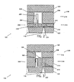
- Figures 2 and 3 are partial cross sections of the gyro showing two example configurations of the ring resonator 104 (204 and 304), ring resonator center mount 106 (206 and 306), spacer 108 (208 and 308), drive/sense electrodes 110 (210 and 310) and sealing ring 112 (212 and 312).
- the ring resonator 204, ring resonator center mount 206, drive/sense electrodes 210 and sealing ring 212 are formed in the device layer 214 of an SOI wafer 216.
- the spacer 208 is formed in a handle layer 218 of the SOI wafer 216.
- the folded cylinder suspension 202 is formed by deposition of a material such as epi-poly silicon in a cavity formed in both the device and handle layers 214 and 218, respectively, of the SOI wafer 216.
- the cavity is lined with a sacrificial layer such as a silicon dioxide which is subsequently removed to release the ring resonator 204 and folded cylinder suspension 202. In this configuration the sacrificial layer and the epi-poly silicon deposition must uniformly bridge the interface between the device and handle layers 214 and 218 of the SOI wafer 216.
- the ring resonator 304, ring resonator center mount 306, drive/sense electrodes 310 and sealing ring 312 are formed in the handle layer 318 of an SOI wafer 316.
- the spacer 308 is formed in the device layer 314. This configuration allows the ring resonator 304 to have a higher aspect ratio providing more mass for a given resonant frequency and increased out-of-plane stiffness.
- the folded cylinder suspension 102 substantially reduces the non-linear spring stiffening effect associated with the single cylinder suspension in much the same manner that the folded beam suspension substantially reduces the same effect in current MEMS gyros. Since both ends of the beam or cylinder originate from a common line or plane the center of the folded beam or cylinder is free to accommodate the lateral in plane motion without introducing tension in the beam or cylinder. An additional feature of the folded cylinder suspension is the increased compliance of the suspension for a given SOI thickness.
- the electronics to operate the ring resonator gyro 100 in one example are identical to that used to operate a hemispheric resonator gyro except for the changes necessary to accommodate the difference in resonant frequency and pickoff and forcer scaling.
- the following fabrication sequence describes example steps to fabricate a single ring resonator sensor chip of the configuration shown in Figure 2 .
- Multiple chips in one example will be fabricated on a single silicon wafer. The number of chips will depend on the wafer diameter.
- the following fabrication sequence describes example steps to fabricate a single ring resonator sensor chip of the configuration shown in Figure 3 .
- Multiple chips in one example will be fabricated on a single silicon wafer. The number of chips will depend on the wafer diameter.
Landscapes
- Physics & Mathematics (AREA)
- Engineering & Computer Science (AREA)
- General Physics & Mathematics (AREA)
- Radar, Positioning & Navigation (AREA)
- Remote Sensing (AREA)
- Gyroscopes (AREA)
Claims (19)
- Ringresonatorkreisel (100) mit:einer Faltzylinder-Aufhängung (102, 202, 302), die einen zylindrischen Ringresonator (104, 204, 304) haltert und eine seitliche in einer Ebene liegende Bewegung des zylindrischen Ringresonators ermöglicht;wobei die Faltzylinder-Aufhängung einen inneren Zylinder, einen äußeren Zylinder und einen Kreisring umfasst;wobei der innere Zylinder, der äußere Zylinder und der Kreisring konzentrisch sind;wobei eine Oberkante des inneren Zylinders mit einer Innenkante des Kreisrings gekoppelt ist;wobei eine Oberkante des äußeren Zylinders mit einer Außenkante des Kreisrings gekoppelt ist.
- Ringresonatorkreisel nach Anspruch 1, bei dem der innere Zylinder und der äußere Zylinder eine im Wesentlichen gleiche Höhe aufweisen.
- Ringresonatorkreisel nach Anspruch 1, bei dem der zylindrische Ringresonator mit einer Unterkante des äußeren Zylinders gekoppelt ist.
- Ringresonatorkreisel nach Anspruch 3, der weiterhin Folgendes umfasst:eine Zentralbefestigung (106, 206, 306);wobei eine Unterkante des inneren Zylinders mit der Zentralbefestigung gekoppelt ist.
- Ringresonatorkreisel nach Anspruch 4, der weiterhin Folgendes umfasst:ein Abstandsstück (108, 208, 308), eine Mehrzahl von Antriebs-/Mess-Elektroden (110, 210, 310), und einen Dichtungsring (112, 212, 312);wobei der zylindrische Ringresonator, die Zentralbefestigung, das Abstandsstück, die Mehrzahl von Antriebs-/Mess-Elektroden und der Dichtungsring in einer Bauteil-Schicht (214) einer SOI-Halbleiterscheibe (216) ausgebildet sind.
- Ringresonatorkreisel nach Anspruch 5, bei dem die Faltzylinderaufhängung in einem Hohlraum der Bauteil-Schicht der SOI-Halbleiterscheibe und einer Handhabungs-Schicht (218) der SOI-Halbleiterscheibe ausgebildet ist.
- Ringresonatorkreisel nach Anspruch 4, der weiterhin Folgendes umfasst:ein Abstandsstück (108, 208, 308) eine Mehrzahl von Antriebs-/Mess-Elektroden (110, 210, 310), und einen Dichtungsring (112, 212, 312);wobei der zylindrische Ringresonator, die Zentralbefestigung, das Abstandsstück, die Mehrzahl von Antriebs-/Mess-Elektroden und der Dichtungsring in einer Handhabungs-Schicht (318) einer SOI-Halbleiterscheibe (316) ausgebildet sind.
- Ringresonatorkreisel nach Anspruch 7, bei dem die Faltzylinderaufhängung in einem Hohlraum der Handhabungs-Schicht gebildet ist.
- Ringresonatorkreisel nach Anspruch 4, bei dem die Faltzylinderaufhängung durch die Verwendung einer Opferschicht gebildet ist, die in einem kreisförmigen Hohlraum abgeschieden ist;
wobei eine Breite des kreisförmigen Hohlraumes auf einer Wandstärke der Opferschicht und einer Dicke der Faltzylinderaufhängung beruht. - Verfahren zur Herstellung eines Ringresonatorkreisels (100), gekennzeichnet durch die folgenden Schritte:Musterbildung und Ätzen eines ersten kreisförmigen Hohlraumes durch eine Oberfläche einer SOI-Halbleiterscheibe (216, 316);Abscheiden oder Aufwachsen einer Opferschicht auf der Oberfläche des SOI-Halbleiterplättchen und in dem ersten kreisförmigen Hohlraum;Entfernen der Opferschicht von der SOI-Halbleiterscheibe;Abscheiden einer Schicht von Epi-Polysilizium auf die Oberfläche der SOI-Halbleiterscheibe und in dem ersten kreisförmigen Hohlraum, wobei ein Teil der Schicht aus Epi-Polysilizium eine Faltzylinderaufhängung (102, 202, 302) umfasst, die einen inneren Zylinder, einen äußeren Zylinder und einen Kreisring umfasst;wobei der innere Zylinder, der äußere Zylinder und der Kreisring konzentrisch sind;wobei eine Oberkante des inneren Zylinders mit einer Innenkante des Kreisrings gekoppelt ist;wobei eine Oberkante des äußeren Zylinders mit einer Außenkante des Kreisrings gekoppelt ist;wobei das Verfahren weiterhin durch die folgenden Schritte gekennzeichnet ist:Musterbildung und Ätzen eines Ringresonators (104, 204, 304) durch die Schicht aus Epi-Polysilizium hindurch;Musterbildung und Ätzen eines oder mehrerer Fenster in der SOI-Halbleiterscheibe, wobei das eine oder die mehreren Fenster konzentrisch sind;Ätzen der Opferschicht, die die Faltzylinderaufhängung umgibt, um den Ringresonator, die Faltzylinderaufhängung und eine Zentralbefestigung (106, 206, 306) freizulegen, wobei die Faltzylinderaufhängung den Ringresonator haltert und eine seitliche in der Ebene liegende Bewegung des Ringresonators ermöglicht.
- Verfahren nach Anspruch 10, bei dem der Schritt der Musterbildung und des Ätzens des ersten kreisförmigen Hohlraumes den Schritt der:Musterbildung und des Ätzens eines ersten kreisförmigen Hohlraums durch die Bauteil-Schicht (214) der SOI-Halbleiterscheibe hindurch und in eine Handhabungsschicht (216) der SOI-Halbleiterscheibe bis zu einer Tiefe umfasst, die kleiner als die Dicke der Handhabungsschicht ist;wobei der Schritt der Entfernung der Opferschicht den Schritt der:Entfernung der Opferschicht von der Oberfläche der Bauteil-Schicht umfasst;wobei der Schritt der Musterbildung und des Ätzens des Ringresonators:das Musterbilden und Ätzen des Ringresonators durch die Schicht aus Epi-Polysilizium und die Bauteil-Schicht hindurch bis herunter zu einer ersten Isolierschicht der SOI-Halbleiterscheibe umfasst;wobei der Schritt der Musterbildung und des Ätzens des einen oder mehreren Fensters:die Musterbildung und das Ätzen eines zweiten kreisförmigen Hohlraums durch die Handhabungsschicht hindurch bis zu der ersten Isolierschicht der SOI-Halbleiterscheibe umfasst, wobei der erste kreisförmige Hohlraum und der zweite kreisförmige Hohlraum konzentrisch sind;wobei der Schritt des Ätzens der Opferschicht, die die Faltzylinder-Aufhängung umgibt, Folgendes umfasst:Ätzen der die Faltzylinder-Aufhängung umgebenden Opferschicht und der ersten Isolierschicht der SOI-Halbleiterschicht zur Freilegung des Ringresonators, der Faltzylinder-Aufhängung und einer Zentralbefestigung (106, 206, 306).
- Verfahren nach Anspruch 11, bei dem der Schritt der Musterbildung und des Ätzens des Ringresonators durch die Schicht von Epi-Polysilizium und die Bauteil-Schicht hindurch bis herunter zu der ersten Isolierschicht der SOI-Halbleiterscheibe den folgenden Schritt umfasst:Musterbildung und Ätzen des Ringresonators und einer Mehrzahl von Antriebs-/Messelektroden (110, 210, 310) durch die Schicht aus Epi-Polysilizium und die Bauteil-Schicht hindurch bis herunter zu der ersten Isolierschicht der SOI-Halbleiterscheibe.
- Verfahren nach Anspruch 12, dass weiterhin die folgenden Schritte umfasst:Abscheiden oder Aufwachsen einer zweiten Isolierschicht auf sowohl einer oberen Deck-Halbleiterscheibe (120) und einer unteren Deck-Halbleiterscheibe (122);Bonden der unteren Deckschicht mit der Bauteil-Schicht der SOI-Halbleiterscheibe;Bonden der oberen Deck-Halbleiterscheibe mit der Handhabungsschicht der SOI-Halbleiterscheibe;Bilden von Durchgangsverbindungen (116) in der unteren Deck-Halbleiterscheibe zur Herstellung eines elektrischen Kontaktes mit der Mehrzahl von Antriebs-/Messelektroden und der Zentralbefestigung.
- Verfahren nach Anspruch 11, bei dem der Schritt der Musterbildung und des Ätzens des ersten kreisförmigen Hohlraumes durch die Bauteil-Schicht der SOI-Halbleiterscheibe hindurch und in die Handhabungsschicht der SOI-Halbleiterscheibe bis zu der Tiefe, die kleiner als die Dicke der Handhabungsschicht ist, den Schritt der:Verwendung einer Tief-Reaktions-Ionenätzung zur Musterbildung und zum Ätzen des ersten kreisförmigen Hohlraumes durch die Bauteil-Schicht der SOI-Halbleiterscheibe hindurch und in die Handhabungsschicht der SOI-Halbleiterscheibe umfasst.
- Verfahren nach Anspruch 10, bei dem der Schritt des Abscheidens oder Aufwachsen der Opferschicht auf die SOI-Halbleiterscheibe und in dem ersten kreisförmigen Hohlraum den Schritt der:Abscheidung oder des Aufwachsens einer Opfer-Siliziumdioxid-Schicht auf die SOI-Halbleiterscheibe und in den ersten kreisförmigen Hohlraum umfasst.
- Verfahren nach Anspruch 10, bei dem der Schritt der Musterbildung und des Ätzens des ersten kreisförmigen Hohlraumes Folgendes umfasst:Musterbildung und Ätzen eines ersten kreisförmigen Hohlraums durch eine Handhabungsschicht hindurch bis zu einer ersten Isolierschicht der SOI-Halbleiterscheibe;wobei der Schritt der Entfernung der Opferschicht Folgendes umfasst:Entfernen der Opferschicht von einer Oberfläche der Handhabungsschicht;wobei der Schritt der Musterbildung und des Ätzens eines Ringresonators:die Musterbildung und das Ätzen eines Ringresonators durch die Schicht aus Epi-Polysilizium und die Handhabungsschicht hindurch bis herunter zu der ersten Isolierschicht der SOI-Halbleiterscheibe umfasst;wobei der Schritt der Musterbildung und des Ätzens eines oder mehrerer Fenster:die Musterbildung und das Ätzen einer Mehrzahl von Fenstern durch die Bauteil-Schicht hindurch zu der ersten Isolierschicht der SOI-Halbleiterscheibe umfasst, wobei die Mehrzahl von Fenstern konzentrisch zu dem ersten kreisförmigen Hohlraum ist, wobei die Mehrzahl von Fenstern die Opferschicht um die Faltzylinder-Aufhängung und die erste Isolierschicht der SOI-Halbleiterscheibe freilegt;wobei der Schritt des Ätzens der Opferschicht, die die Faltzylinder-Aufhängung umgibt:das Ätzen der Opferschicht um die Faltzylinder-Aufhängung herum und die erste Isolierschicht der SOI-Halbleiterscheibe umfasst, um den Ringresonator, die Faltzylinder-Aufhängung und die Zentralbefestigung freizulegen.
- Verfahren nach Anspruch 16, bei dem der Schritt der Musterbildung und des Ätzens des Ringresonators durch die Schicht aus Epi-Polysilizium und die Handhabungsschicht hindurch bis herunter zu der ersten Isolierschicht der SOI-Halbleiterscheibe den Schritt der:Musterbildung und des Ätzens des Ringresonators und einer Mehrzahl von Antriebs-/Messelektroden durch die Schicht aus Epi-Polysilizium und die Handhabungsschicht hindurch bis herunter zu der ersten Isolierschicht der SOI-Halbleiterscheibe umfasst.
- Verfahren nach Anspruch 17, dass weiterhin die folgenden Schritte umfasst:Abscheiden oder Aufwachsen einer zweiten Isolierschicht sowohl auf eine obere Deck-Halbleiterscheibe (120) als auch eine untere Deck-Halbleiterscheibe (122);Bonden der unteren Deck-Halbleiterscheibe an die Handhabungsschicht der SOI-Halbleiterscheibe;Bonden der oberen Deck-Halbleiterscheibe an die Bauteil-Schicht der SOI-Halbleiterscheibe;Bilden von Durchgangsverbindungen (116) in der unteren Deck-Halbleiterscheibe zur Herstellung eines elektrischen Kontaktes mit der Mehrzahl von Antriebs-/Messelektroden und der Zentralbefestigung.
- Verfahren nach Anspruch 16, bei dem der Schritt der Musterbildung und des Ätzens des ersten kreisförmigen Hohlraums durch die Handhabungsschicht hindurch zu der ersten Isolierschicht der SOI-Halbleiterscheibe den Schritt der:Verwendung einer Tief-Reaktions-Ionenätzung zur Musterbildung und zum Ätzen des ersten kreisförmigen Hohlraums durch die Handhabungsschicht hindurch zu der ersten Isolierschicht der SOI-Halbleiterscheibe umfasst.
Applications Claiming Priority (1)
| Application Number | Priority Date | Filing Date | Title |
|---|---|---|---|
| US70684905P | 2005-08-08 | 2005-08-08 |
Publications (3)
| Publication Number | Publication Date |
|---|---|
| EP1752736A2 EP1752736A2 (de) | 2007-02-14 |
| EP1752736A3 EP1752736A3 (de) | 2008-06-18 |
| EP1752736B1 true EP1752736B1 (de) | 2011-03-09 |
Family
ID=37442079
Family Applications (1)
| Application Number | Title | Priority Date | Filing Date |
|---|---|---|---|
| EP06254172A Not-in-force EP1752736B1 (de) | 2005-08-08 | 2006-08-08 | Ringresonatorkreisel mit Faltzylinderaufhängung |
Country Status (4)
| Country | Link |
|---|---|
| US (1) | US7426860B2 (de) |
| EP (1) | EP1752736B1 (de) |
| JP (1) | JP4871065B2 (de) |
| DE (1) | DE602006020526D1 (de) |
Families Citing this family (7)
| Publication number | Priority date | Publication date | Assignee | Title |
|---|---|---|---|---|
| US8109145B2 (en) * | 2007-07-31 | 2012-02-07 | Northrop Grumman Guidance And Electronics Company, Inc. | Micro hemispheric resonator gyro |
| US8011246B2 (en) * | 2008-09-22 | 2011-09-06 | Northrop Grumman Guidance And Electronics Company, Inc. | Apparatus and method for self-calibration of coriolis vibratory gyroscope |
| US8393212B2 (en) * | 2009-04-01 | 2013-03-12 | The Boeing Company | Environmentally robust disc resonator gyroscope |
| RU2413926C1 (ru) * | 2009-12-24 | 2011-03-10 | Государственное образовательное учреждение высшего профессионального образования Московский государственный институт электронной техники (технический университет) (МИЭТ) | Чувствительный элемент кольцевого микромеханического вибрационного гироскопа |
| US8763441B2 (en) * | 2011-11-22 | 2014-07-01 | Georgia Tech Research Corporation | Method and apparatus for self-calibration of gyroscopes |
| CN107063224B (zh) * | 2016-12-12 | 2020-06-23 | 北京自动化控制设备研究所 | 一种soi微半球陀螺敏感结构 |
| CN114964192B (zh) * | 2022-07-26 | 2022-10-14 | 深圳市景创科技电子股份有限公司 | 新型陀螺仪结构及装置 |
Family Cites Families (13)
| Publication number | Priority date | Publication date | Assignee | Title |
|---|---|---|---|---|
| GB8404668D0 (en) * | 1984-02-22 | 1984-03-28 | Burdess J S | Gyroscopic devices |
| JPH08271258A (ja) * | 1995-03-28 | 1996-10-18 | Taiyo Yuden Co Ltd | リング状振動子の支持構造 |
| DE19617666B4 (de) | 1996-05-03 | 2006-04-20 | Robert Bosch Gmbh | Mikromechanischer Drehratensensor |
| GB2318184B (en) * | 1996-10-08 | 2000-07-05 | British Aerospace | A rate sensor |
| JPH10115526A (ja) * | 1996-10-15 | 1998-05-06 | Ngk Insulators Ltd | 振動ジャイロ・センサ及び振動ジャイロ・センサの製造方法 |
| US6128954A (en) * | 1998-12-18 | 2000-10-10 | Delco Electronics Corporation | Spring for a resonance ring of an angular rate sensor |
| US6481285B1 (en) | 1999-04-21 | 2002-11-19 | Andrei M. Shkel | Micro-machined angle-measuring gyroscope |
| JP2001108442A (ja) * | 1999-10-06 | 2001-04-20 | Japan Aviation Electronics Industry Ltd | 振動型角速度センサ励振方法・振動型角速度センサ |
| JP2001304869A (ja) * | 2000-04-21 | 2001-10-31 | Japan Aviation Electronics Industry Ltd | リング型振動式レートセンサ |
| DE60232250D1 (de) * | 2001-08-20 | 2009-06-18 | Honeywell Int Inc | Bogenförmige federelemente für mikro-elektromechanischen beschleunigungssensor |
| GB0122254D0 (en) * | 2001-09-14 | 2001-11-07 | Bae Systems Plc | Vibratory gyroscopic rate sensor |
| US6934660B2 (en) * | 2003-02-20 | 2005-08-23 | The Regents Of The University Of California | Multi stage control architecture for error suppression in micromachined gyroscopes |
| JP2005031097A (ja) * | 2004-09-27 | 2005-02-03 | Kazuhiro Okada | 加速度と角速度との双方を検出する装置 |
-
2006
- 2006-08-07 US US11/499,959 patent/US7426860B2/en not_active Expired - Fee Related
- 2006-08-08 JP JP2006216271A patent/JP4871065B2/ja not_active Expired - Fee Related
- 2006-08-08 EP EP06254172A patent/EP1752736B1/de not_active Not-in-force
- 2006-08-08 DE DE602006020526T patent/DE602006020526D1/de active Active
Also Published As
| Publication number | Publication date |
|---|---|
| US7426860B2 (en) | 2008-09-23 |
| DE602006020526D1 (de) | 2011-04-21 |
| US20070034006A1 (en) | 2007-02-15 |
| JP2007052014A (ja) | 2007-03-01 |
| EP1752736A3 (de) | 2008-06-18 |
| JP4871065B2 (ja) | 2012-02-08 |
| EP1752736A2 (de) | 2007-02-14 |
Similar Documents
| Publication | Publication Date | Title |
|---|---|---|
| EP0902875B1 (de) | Aus silizium in mikrotechnologie hergestellter symmetrischer vibrationskreiselsensor | |
| US7347095B2 (en) | Integral resonator gyroscope | |
| US8205495B2 (en) | Systematic disc resonator gyroscope tuning | |
| US7401397B2 (en) | Method of producing an inertial sensor | |
| US6796179B2 (en) | Split-resonator integrated-post MEMS gyroscope | |
| US7624494B2 (en) | Method of fabricating a mesoscaled resonator | |
| EP2028440B1 (de) | Integralträgheitsmesseinheit für Scheibenresonator | |
| US8166816B2 (en) | Bulk acoustic wave gyroscope | |
| US7818871B2 (en) | Disc resonator gyroscope fabrication process requiring no bonding alignment | |
| Tang et al. | Silicon bulk micromachined vibratory gyroscope for microspacecraft | |
| JP2004537733A (ja) | 隔離された共振器ジャイロスコープ | |
| WO2006009578A2 (en) | High-resolution in-plane tuning fork gyroscope and methods of fabrication | |
| US7434465B1 (en) | Ring resonator gyroscope with cylindrical ring suspension | |
| JP4698221B2 (ja) | 内部径方向検知およびアクチュエーションを備える分離型平面ジャイロスコープ | |
| Antonello et al. | MEMS gyroscopes for consumers and industrial applications | |
| EP1752736B1 (de) | Ringresonatorkreisel mit Faltzylinderaufhängung | |
| EP1754953B1 (de) | Ringresonatorkreisel mit Zylinderringaufhängung | |
| Shcheglov et al. | Isolated planar gyroscope with internal radial sensing and actuation | |
| WO2005100237A1 (en) | Isolated planar mesogyroscope | |
| EP1571416B1 (de) | Unterstützung eines vibrierenden Balkens nahe einem Knotenpunt | |
| Le Traon et al. | GYTRIX Quartz MEMS Gyro: From Concept to Northfinding Measurements | |
| Shcheglov et al. | Method of producing an integral resonator sensor and case | |
| Shcheglov et al. | Integral resonator gyroscope | |
| Shcheglov et al. | Method of producing an inertial sensor |
Legal Events
| Date | Code | Title | Description |
|---|---|---|---|
| PUAI | Public reference made under article 153(3) epc to a published international application that has entered the european phase |
Free format text: ORIGINAL CODE: 0009012 |
|
| AK | Designated contracting states |
Kind code of ref document: A2 Designated state(s): AT BE BG CH CY CZ DE DK EE ES FI FR GB GR HU IE IS IT LI LT LU LV MC NL PL PT RO SE SI SK TR |
|
| AX | Request for extension of the european patent |
Extension state: AL BA HR MK YU |
|
| PUAL | Search report despatched |
Free format text: ORIGINAL CODE: 0009013 |
|
| AK | Designated contracting states |
Kind code of ref document: A3 Designated state(s): AT BE BG CH CY CZ DE DK EE ES FI FR GB GR HU IE IS IT LI LT LU LV MC NL PL PT RO SE SI SK TR |
|
| AX | Request for extension of the european patent |
Extension state: AL BA HR MK RS |
|
| RIC1 | Information provided on ipc code assigned before grant |
Ipc: G01C 19/56 20060101AFI20061130BHEP |
|
| 17P | Request for examination filed |
Effective date: 20080922 |
|
| 17Q | First examination report despatched |
Effective date: 20081105 |
|
| AKX | Designation fees paid |
Designated state(s): DE FR GB IT |
|
| GRAP | Despatch of communication of intention to grant a patent |
Free format text: ORIGINAL CODE: EPIDOSNIGR1 |
|
| GRAS | Grant fee paid |
Free format text: ORIGINAL CODE: EPIDOSNIGR3 |
|
| GRAA | (expected) grant |
Free format text: ORIGINAL CODE: 0009210 |
|
| AK | Designated contracting states |
Kind code of ref document: B1 Designated state(s): DE FR GB IT |
|
| REG | Reference to a national code |
Ref country code: GB Ref legal event code: FG4D |
|
| REF | Corresponds to: |
Ref document number: 602006020526 Country of ref document: DE Date of ref document: 20110421 Kind code of ref document: P |
|
| REG | Reference to a national code |
Ref country code: DE Ref legal event code: R096 Ref document number: 602006020526 Country of ref document: DE Effective date: 20110421 |
|
| PLBE | No opposition filed within time limit |
Free format text: ORIGINAL CODE: 0009261 |
|
| STAA | Information on the status of an ep patent application or granted ep patent |
Free format text: STATUS: NO OPPOSITION FILED WITHIN TIME LIMIT |
|
| 26N | No opposition filed |
Effective date: 20111212 |
|
| REG | Reference to a national code |
Ref country code: DE Ref legal event code: R097 Ref document number: 602006020526 Country of ref document: DE Effective date: 20111212 |
|
| REG | Reference to a national code |
Ref country code: FR Ref legal event code: PLFP Year of fee payment: 11 |
|
| REG | Reference to a national code |
Ref country code: FR Ref legal event code: PLFP Year of fee payment: 12 |
|
| REG | Reference to a national code |
Ref country code: FR Ref legal event code: PLFP Year of fee payment: 13 |
|
| PGFP | Annual fee paid to national office [announced via postgrant information from national office to epo] |
Ref country code: FR Payment date: 20190822 Year of fee payment: 14 Ref country code: IT Payment date: 20190829 Year of fee payment: 14 |
|
| PGFP | Annual fee paid to national office [announced via postgrant information from national office to epo] |
Ref country code: GB Payment date: 20190821 Year of fee payment: 14 |
|
| PGFP | Annual fee paid to national office [announced via postgrant information from national office to epo] |
Ref country code: DE Payment date: 20200819 Year of fee payment: 15 |
|
| GBPC | Gb: european patent ceased through non-payment of renewal fee |
Effective date: 20200808 |
|
| PG25 | Lapsed in a contracting state [announced via postgrant information from national office to epo] |
Ref country code: FR Free format text: LAPSE BECAUSE OF NON-PAYMENT OF DUE FEES Effective date: 20200831 Ref country code: IT Free format text: LAPSE BECAUSE OF NON-PAYMENT OF DUE FEES Effective date: 20200808 |
|
| PG25 | Lapsed in a contracting state [announced via postgrant information from national office to epo] |
Ref country code: GB Free format text: LAPSE BECAUSE OF NON-PAYMENT OF DUE FEES Effective date: 20200808 |
|
| REG | Reference to a national code |
Ref country code: DE Ref legal event code: R119 Ref document number: 602006020526 Country of ref document: DE |
|
| PG25 | Lapsed in a contracting state [announced via postgrant information from national office to epo] |
Ref country code: DE Free format text: LAPSE BECAUSE OF NON-PAYMENT OF DUE FEES Effective date: 20220301 |