EP1752306A1 - Mask for laser-induced thermal imaging - Google Patents
Mask for laser-induced thermal imaging Download PDFInfo
- Publication number
- EP1752306A1 EP1752306A1 EP06254231A EP06254231A EP1752306A1 EP 1752306 A1 EP1752306 A1 EP 1752306A1 EP 06254231 A EP06254231 A EP 06254231A EP 06254231 A EP06254231 A EP 06254231A EP 1752306 A1 EP1752306 A1 EP 1752306A1
- Authority
- EP
- European Patent Office
- Prior art keywords
- pattern
- pattern portion
- liti
- mask
- apex
- Prior art date
- Legal status (The legal status is an assumption and is not a legal conclusion. Google has not performed a legal analysis and makes no representation as to the accuracy of the status listed.)
- Granted
Links
Images





Classifications
-
- B—PERFORMING OPERATIONS; TRANSPORTING
- B41—PRINTING; LINING MACHINES; TYPEWRITERS; STAMPS
- B41M—PRINTING, DUPLICATING, MARKING, OR COPYING PROCESSES; COLOUR PRINTING
- B41M5/00—Duplicating or marking methods; Sheet materials for use therein
- B41M5/26—Thermography ; Marking by high energetic means, e.g. laser otherwise than by burning, and characterised by the material used
- B41M5/265—Thermography ; Marking by high energetic means, e.g. laser otherwise than by burning, and characterised by the material used for the production of optical filters or electrical components
-
- H—ELECTRICITY
- H05—ELECTRIC TECHNIQUES NOT OTHERWISE PROVIDED FOR
- H05B—ELECTRIC HEATING; ELECTRIC LIGHT SOURCES NOT OTHERWISE PROVIDED FOR; CIRCUIT ARRANGEMENTS FOR ELECTRIC LIGHT SOURCES, IN GENERAL
- H05B33/00—Electroluminescent light sources
- H05B33/10—Apparatus or processes specially adapted to the manufacture of electroluminescent light sources
-
- B—PERFORMING OPERATIONS; TRANSPORTING
- B41—PRINTING; LINING MACHINES; TYPEWRITERS; STAMPS
- B41M—PRINTING, DUPLICATING, MARKING, OR COPYING PROCESSES; COLOUR PRINTING
- B41M3/00—Printing processes to produce particular kinds of printed work, e.g. patterns
- B41M3/003—Printing processes to produce particular kinds of printed work, e.g. patterns on optical devices, e.g. lens elements; for the production of optical devices
-
- H—ELECTRICITY
- H10—SEMICONDUCTOR DEVICES; ELECTRIC SOLID-STATE DEVICES NOT OTHERWISE PROVIDED FOR
- H10K—ORGANIC ELECTRIC SOLID-STATE DEVICES
- H10K71/00—Manufacture or treatment specially adapted for the organic devices covered by this subclass
- H10K71/10—Deposition of organic active material
- H10K71/18—Deposition of organic active material using non-liquid printing techniques, e.g. thermal transfer printing from a donor sheet
Definitions
- the present invention relates to a Laser Induced Thermal Imaging (LITI) mask and an organic electroluminescent device fabrication method using the mask.
- LITI Laser Induced Thermal Imaging
- An organic electroluminescent device in flat panel displays has merit as a moving picture display media irrespective of the size of the display since the organic electroluminescent device has a high response speed of 1 ms or less, consumes less electrical power than other devices and does not have a viewing angle problem due to its self-light emitting characteristics. Furthermore, the organic electroluminescent device is being considered as a next generation flat panel display because it can be fabricated at a low temperature and is simply fabricated based on an existing semiconductor process technology.
- a patterning technology of an organic film composing the organic electroluminescent device is important in the organic electroluminescent device.
- the Laser Induced Thermal Imaging (LITI) method has excellent pattern uniformity and is advantageous in scaling-up of the organic film.
- the LITI method has excellent inner uniformity of pixels when the organic film is scaled up since spin coating characteristics are used in the LITI method as is. Furthermore, the LITI method is capable of solving a problem of life deterioration of device by preventing damage of the organic film due to a solvent since the LITI method is not a wet process, but is rather a dry process. Additionally, the LITI method has merit in that the organic film can be finely patterned.
- a light source and an organic electroluminescent device substrate i.e., a substrate and a donor substrate
- the donor substrate includes a substrate layer, a light to heat conversion layer and a transfer layer.
- the LITI method includes a step of absorbing light coming out of the light source into the light to heat conversion layer of the donor substrate such that light is converted into thermal energy, and a step of transferring an organic material formed on the transfer layer by the converted thermal energy to the substrate such that the organic film is formed.
- a donor substrate is laminated with a receptor substrate on which a prescribed device is formed.
- the donor substrate includes a substrate layer, a light to heat conversion layer and a transfer layer formed of a material composing an organic layer to be patterned.
- the receptor substrate sequentially includes a substrate, a pixel electrode pattern and a pixel defining layer.
- the pixel defining layer includes an opening for exposing a prescribed portion of the pixel electrode pattern.
- the organic film is patterned by transferring an organic film using a laser, such that a portion of the organic film (the 'transfer layer') receives laser energy passing through a mask having a shape to be patterned, causing the transfer layer to separate from the donor substrate and to be transferred to the receptor substrate, and also causing the transfer layer to be separated from other portions of the organic film which did not receive laser energy.
- the transfer characteristics are determined by a first adhesive force between the receptor substrate and a transfer layer, a cohesive force between the transfer layers, and a second adhesive force between the transfer layer and a substrate; the cohesive force between the transfer layers should be lower than adhesive force between the respective substrates and the transfer layer in order to improve laser transfer characteristics.
- the transfer layer When a transfer layer is transferred to the receptor substrate, the transfer layer may not adhere to the donor substrate in places, owing to the limited degree of ductility of the donor substrate and surface level differences of the receptor substrate.
- the transfer layer may be detached particularly in respect of portions of the receptor substrate that include an apex (which term may connote a corner, or a concave region formed by the intersection of two or more surfaces, for example), resulting in a small contact area between the receptor substrate and the transfer layer compared to other regions. Therefore, in respect of a portion including an apex on one side of the receptor substrate, the foregoing second adhesive force, that is, adhesive force between the receptor substrate and the transfer layer, may be deteriorated.
- the cohesive force between the transfer layers can be higher than the first adhesive force on the portion including an apex on one side of the receptor substrate during a process of adsorbing the donor substrate from the receptor substrate after being irradiated by a laser beam. Therefore, an organic layer pattern is unevenly formed on a portion A including an apex on one side of a pixel portion to result in deterioration of picture quality or the generation of an opening defect in which a prescribed portion of the pixel portion is open on a portion of the organic layer pattern.
- a photolithography mask equipped with a serif for solving the rounding defect when a rounding defect is formed on a semiconductor integrated circuit pattern is suggested in United States Patent No. 5,707,765 .
- the photolithography mask discussed therein is equipped with a serif that is a reinforced region on the edge of a mask pattern to supplement rounding of the pattern caused by an optical problem generated during a fine patterning process, i.e., a proximity effect generated on a portion of pattern due to light diffraction.
- LITI Laser Induced Thermal Imaging
- the present invention provides a Laser Induced Thermal Imaging (LITI) mask, comprising: a first pattern portion; and a second pattern portion arranged on at least one side of the first pattern portion and adjacent to an apex of the first pattern portion; wherein the second pattern portion has an area of between 8 and 8,500 ⁇ m 2 .
- LITI Laser Induced Thermal Imaging
- the present invention provides a Laser Induced Thermal Imaging (LITI) mask, comprising: a first pattern portion; and a second pattern portion arranged on at least one side of the first pattern portion and adjacent to an apex of the first pattern portion; wherein the second pattern portion extends between 2 and 30 ⁇ m from the first pattern portion.
- LITI Laser Induced Thermal Imaging
- the present invention provides a method of fabricating an organic electroluminescent device, comprising: forming a first electrode on a substrate; laminating a donor substrate onto an upper portion of the first electrode formed on the substrate; forming an organic layer pattern by irradiating a laser beam passing through a Laser Induced Thermal Imaging (LITI) mask as aforesaid; and forming a second electrode on an upper portion of the organic layer pattern; wherein a reinforced region having an area of between 8 and 8,500 ⁇ m 2 is formed on a portion arranged on at least one side of the organic layer pattern and adjacent to an apex of the organic layer pattern.
- LITI Laser Induced Thermal Imaging
- FIG. 1A to FIG. 1E are views for explaining a process of forming organic layer patterns by a Laser Induced Thermal Imaging (LITI) method.
- LITI Laser Induced Thermal Imaging
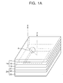
- FIG. 1A is a plan figure in which a donor substrate is laminated with a receptor substrate
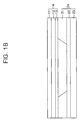
- FIG. 1B is a cross-sectional view taken along a line I-I' of FIG. 1A.
- a donor substrate 14 is laminated with a receptor substrate 24 on which a prescribed device is formed; the donor substrate 14 includes a substrate layer 11, a light to heat conversion layer 12 and a transfer layer 13 formed of a material composing an organic layer to be patterned.
- the receptor substrate 24 sequentially includes a substrate 23, a pixel electrode pattern 22 and a pixel defining layer 21; the pixel defining layer 21 includes an opening for exposing a prescribed portion of the pixel electrode pattern 22.
- FIG. 1C is a cross-sectional view for explaining the process of transferring an organic film by a LITI method.
- the organic film is patterned by transferring an organic film using a laser such that the organic film S2 is separated from a portion which does not receive laser energy while the organic film S2 is being transferred to a receptor substrate S3 24 after an organic film S2 13 adhered to the substrate S1 comes off from a donor substrate S1 by the action of laser energy passing through a mask 30 having a shape to be patterned.
- the transfer characteristics are determined by a first adhesive force W12 between the receptor substrate S1 and a transfer layer S2, a cohesive force W22 between the transfer layers and a second adhesive force W23 between the transfer layer S2 and a substrate S3; the cohesive force between the transfer layers should be lower than adhesive force between the respective substrates and the transfer layer in order to improve laser transfer characteristics.
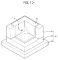
- FIG. 1D is a plan figure of the expanded portion after expanding a portion A including an apex on one side after laser irradiation in FIG. 1C.
- the cohesive force between the transfer layers can be higher than the first adhesive force on the portion A during a process of adsorbing the donor substrate from the receptor substrate 24 after being irradiated by a laser beam. Therefore, an organic layer pattern 13' is unevenly formed on a portion A including an apex on one side of a pixel portion to result in deterioration of picture quality or the generation of an opening defect in which a prescribed portion of the pixel portion is open on a portion of the organic layer pattern 13'.
- FIG. 2A to FIG. 2C are plan figures of various exemplary embodiments of a LITI mask for determining a shape of an organic layer pattern.
- a pattern of the mask has a certain cycle and is formed in a stripe shape (FIG. 2A), mosaic shape (FIG. 2B) or delta shape (FIG. 2C) according to patterns of an emitting layer of an organic electroluminescent device.
- the mask pattern has a cycle in which the same pattern as a first pattern group 1 is repeated in case of a stripe shaped mask of FIG. 2A, and the mask pattern is formed in a shape in which the first pattern group 1, a second pattern group 2 and a third pattern group 3 are repeated as one cycle in case of a mosaic shaped mask of FIG. 2B. Furthermore, the mask pattern is formed in a shape in which the first pattern group 1 and the second pattern group 2 are repeated as one cycle in case of a delta shaped mask of FIG. 2C.
- the mosaic shaped mask and the delta shaped mask are used to form an organic layer for a multicolored organic electroluminescent device
- the stripe shaped mask is used to form an organic layer for both a single colored organic electroluminescent device and a multicolored organic electroluminescent device.
- FIG. 3A to FIG. 3E are views for explaining various shaped patterns of a LITI mask capable of being applied according to exemplary embodiments of the present invention; the various shaped patterns of the LITI mask are explained are limited to the case in which a projection lens of a laser irradiation apparatus is an equal-magnification projection lens although it is not illustrated in the drawings.
- the masks are differently designed according to the magnification of the projection lens. For example, when a magnification of the projection lens is 2:1, the LITI mask is designed such that area of the mask is quadrupled, and length of the mask is doubled.
- a laser beam passing through the mask is irradiated onto a pixel portion 40 in the same shape as the mask pattern 50.
- the mask pattern 50 includes of a first pattern portion 20 having a prescribed shape that transmits light, and a second pattern portion 30 for reinforcing a portion including an apex on at least one side of the first pattern portion 20, wherein the second pattern portion 30 is preferably formed on the portion including an apex on at least one side of the first pattern portion 20.
- the second pattern portion 30 can be formed on the upper surface and the lower surface of the first pattern portion 20.
- the first pattern portion 20 is designed such that the first pattern portion 20 is bigger than the pixel portion 40 considering misalignment of patterns. That is, length L and width H of the first pattern portion 20 are ordinarily extended 2 to 30 ⁇ m from respective side surfaces of the pixel portion 40.
- length a of the second pattern portion 30 reinforced on the portion including an apex on at least one side of the first pattern portion is projected 2 to 30 ⁇ m from the portion including an apex on at least one side of the first pattern portion so as to prevent formation of an opening defect or uneven patterns due to deterioration of the adhesive force caused by decreasing the area of a transfer layer to be adhered to a receptor substrate after being separated from a donor substrate on the portion including an apex on at least one side of the first pattern portion as compared with other regions.
- the length a of the second pattern portion 30 reinforced on the portion including an apex on at least one side of the first pattern portion is projected 2 ⁇ m or less from the portion including an apex on at least one side of the first pattern portion, the area of the transfer layer to be adhered to the receptor substrate after being separated from the donor substrate is increased.
- the adhesive force between the transfer layer and a portion including an apex on one side of the receptor substrate is not improved enough to solve the foregoing problem.
- the transfer layer can be overlapped with a pixel portion formed adjacently to the transfer layer although area of the transfer layer contacted with the receptor substrate after being separated from the donor substrate is increased such that uniform patterns are formed, and an opening defect is prevented from being formed.
- length b of the second pattern portion 30 is preferably projected 4 to 60 ⁇ m from a portion including an apex on at least one side of the first pattern portion considering that the second pattern portion is capable of sufficiently preventing an opening defect from forming on corners.
- An area range of the second pattern portion to be reinforced can be obtained. That is, the area of the second pattern portion 30 to be obtained is ab, wherein the area range of the second pattern portion is 8 to 1,800 ⁇ m 2 since a satisfies 2 ⁇ m ⁇ a ⁇ 30 ⁇ m, and b satisfies 4 ⁇ m ⁇ b ⁇ 60 ⁇ m. Namely, a prescribed shaped second pattern portion having the above area range is formed to prevent an opening defect from forming on a portion including an apex on at least one side due to the deterioration of the adhesive force.
- the second pattern portion 30 can be formed on the left side surface and the right side surface of the first pattern portion 20, wherein length a of the second pattern portion 30 reinforced on a portion including an apex on at least one side of the first pattern portion 20 is preferably projected 2 to 30 ⁇ m perpendicularly from corners. Furthermore, length b of the first pattern portion is preferably projected 4 to 60 ⁇ m from the portion including an apex on at least one side of the first pattern portion 20 to sufficiently prevent an opening defect from forming on the portion including an apex on at least one side of the first pattern portion 20.
- the second pattern portion 30 reinforced on the portion including an apex on at least one side of the first pattern portion 20 preferably has an area of 8 to 1,800 ⁇ m 2 to prevent formation of an opening defect.
- FIG. 3C constructed in a combined structure of FIG. 3A and FIG. 3B has the same constitutional factors and reference numbers as in FIG. 3A and FIG. 3B, a repeated description has been omitted.
- second pattern portions 30 are formed on side surfaces of a portion including an apex on at least one side of a first pattern portion 20, wherein the area of the second pattern portion 30 reinforced on the portion including an apex on at least one side of the first pattern portion 20 is increased to a range of 16 to 3,600 ⁇ m 2 to further increase the adhesive force of a transfer layer separated from a substrate and a donor substrate on the portion including an apex on at least one side of the first pattern portion 20.
- the second pattern portions 30 are formed on the side surfaces of the portion including an apex on at least one side of the first pattern portion 20 such that portions of the second pattern portions are overlapped with the portion including an apex on at least one side of the first pattern portion 20. That is, the second pattern portion 30 is formed such that the second pattern portion 30 surrounds the portion including an apex on at least one side of the first pattern portion 20, wherein the second pattern portion 30 reinforced on the portion including an apex on at least one side of the first pattern portion 20 preferably has an area of 12 to 2,700 ⁇ m 2 .
- an opening defect can be formed on the portion including an apex on at least one side of the first pattern portion 20. Therefore, the opening defect can be completely prevented from being formed by further forming an extra reinforcement region on the portion including an apex on at least one side of the first pattern portion 20.
- the second pattern portion 30 is formed around an apex of the first pattern portion 20 in a circular shape such that a radius R of the second pattern portion 30 is L+H. That is, the radius R of the second pattern portion is from 4 to 60 ⁇ m, and the second pattern portion 30 has an area of 37 to 8,500 ⁇ m 2 to increase the adhesive force of a transfer layer separated from a receptor substrate and a donor substrate accordingly. Furthermore, more uniformed patterns can be formed by reinforcing the second pattern portion 30 in a circular shape on respective regions of a portion including an apex on one side such that the second pattern portion has uniform length, thereby giving a uniform adhesive force to corners.
- the second pattern portion 30 is illustrated as a rectangular or circular shape in the drawings, the second pattern portion is not limited to the rectangular or circular shape since an organic layer pattern formed by the second pattern portion is a non-emitting region.
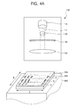
- FIG. 4A to FIG. 4C are drawings for explaining an organic electroluminescent device fabrication method according to exemplary embodiments of the present invention.
- a LITI device 100 includes a laser generator 110, a LITI mask 130 installed under the laser generator 110, and a projection lens 140; the LITI device 100 further includes a beam shaper, not illustrated in FIG. 4A, installed between the laser generator 110 and the LITI mask 130 to cause a uniform laser beam 111 to be irradiated from the laser generator 110.
- a substrate 200 having a pixel electrode under the LITI device 100 is laminated with a donor substrate 250 having at least one transfer layer above the substrate 200.
- a laser beam 111 is produced by the laser generator 110, and the laser beam 111 passes through the LITI mask 130 that is patterned in a prescribed shape; the laser beam 111 transmits a pattern group of the LITI mask 130 having patterns 1, 2, 3, ..., n that are repeated in a certain cycle such that the laser beam is patterned in a shape of the LITI mask 130.
- the laser beam 111 passing through the LITI mask 130 reaches the donor substrate by being transmitted through the projection lens.
- a mosaic, delta or stripe shaped pattern is formed on an upper portion of the substrate 200 according to shape of the LITI mask.
- a first pattern group a is completed on an upper portion of the substrate 200 through the foregoing process.
- the LITI device After forming the first pattern group a, the LITI device is moved in a direction II, and the mask 130 installed in the LITI device is moved a fixed distance in a transfer direction I.
- the laser beam is patterned by transmitting the laser beam 111 through a repeated pattern group of the mask 130, and a second pattern group b is formed on an upper portion of the substrate 200 by irradiating the patterned laser beam onto an upper portion of the donor substrate 250.
- the LITI device is again moved in the direction II, and the LITI mask 130 installed in the LITI device is again moved a fixed distance in the transfer direction I.
- the laser beam is patterned by transmitting the laser beam 111 through a repeated pattern group of the LITI mask 130, and a third pattern group c is formed on an upper portion of the substrate 200 by irradiating the patterned laser beam onto an upper portion of the donor substrate 250.
- the foregoing process is capable of moving the stage and the LITI mask 130 such that the movement of a stage 300 along the substrate is synchronized with the movement of the LITI mask 130 or moving the stage and the LITI mask 130 while respective groups are being moved one step at a time.
- An organic film illustrated in the drawings, is patterned on an upper portion of the substrate 200 when the transfer in the direction TT has been completed by repeating the foregoing process.
- the organic layer pattern can be an emitting layer.
- the organic layer pattern further includes one or more layers selected from the group consisting of a hole injection layer, a hole transport layer, a hole inhibition layer and an electron injection layer.
- FIG. 4B and FIG. 4C are respective views of a donor substrate and a substrate laminated with a mask as perspective views for expanding one unit pixel A in FIG. 4A.
- the foregoing LITI mask 130 includes a first pattern portion 131, and a second pattern portion 132 for reinforcing a portion including an apex on at least one side of the first pattern portion 131.
- a laser beam 111 is irradiated onto the donor substrate 250 according to the shape of the first pattern portion 131 and the second pattern portion 132 of the LITI mask 130; the donor substrate 250 includes at least a substrate layer 260, a light to heat conversion layer 270 and a transfer layer 280. Furthermore, a receptor substrate 200 is laminated on a lower portion of the donor substrate 250.
- the receptor substrate 200 includes a substrate 210, a pixel electrode 220 formed on the substrate 210, and a pixel defining layer 230 formed on the pixel electrode 220 to define a pixel portion 300.
- the laser beam 111 projected on the donor substrate 250 is absorbed into the light to heat conversion layer 270 of the donor substrate 250 such that the laser beam 111 absorbed into the light to heat conversion layer 270 is converted into heat.
- the heat has an effect on the transfer layer 280 such that the transfer layer is separated from the donor substrate 250 and transferred onto the pixel electrode 220 of the receptor substrate 200.
- the transfer layer transferred onto the pixel electrode 220 can come off a portion including an apex on one side due to a surface level difference of the receptor substrate 200. Although an area of a transfer layer transferred onto the portion including an apex on one side can be decreased compared with area of a transfer layer transferred onto other regions, the area of a transfer layer transferred onto the portion including an apex on one side is not decreased by the second pattern 132 reinforced on a portion including an apex on at least one side of the first pattern portion 131 of the mask.
- an adhesion area of a transfer layer transferred onto the portion including an apex on at least one side is increased during separation of the receptor substrate 200 and the donor substrate 250 to prevent an opening defect or uneven patterns from forming on a portion of the pixel electrode 220.
- an organic layer 280' can be patterned and formed in a pattern shape of the mask on the pixel electrode 220. That is, a first organic layer pattern portion 131' is formed by a first pattern portion 131 in FIG. 4B of the mask. Furthermore, a second organic pattern portion 132' in which a portion including an apex on at least one side of the first organic layer pattern portion 131' is reinforced is formed by a second pattern portion 132 in FIG. 4B of the mask; the second organic pattern portion 132' does not have an effect on an organic electroluminescent device since the second organic pattern portion 132' is formed on a non-emitting portion.
- a transfer process of forming an organic layer pattern by the LITI device can be performed in a nitrogen atmosphere to prevent the organic layer pattern from being oxidized by oxygen existing in the atmosphere; it is preferable to charge nitrogen gas (N2) until an atmosphere containing 100 ppm of 02 and 100 ppm of H2O is created considering conditions in which the organic film is not influenced by oxygen or moisture since a considerable amount of time and money have to be invested to create a nitrogen atmosphere.
- nitrogen gas N2
- the transfer process is performed in a vacuum atmosphere such that the generation of air bubbles between the donor substrate and the substrate can be suppressed during a process of laminating the donor substrate onto the front of the substrate.
- an organic electroluminescent device is completed by forming patterns a, b and c of an organic film having certain cycles on an upper portion of a substrate 200 and forming an upper electrode, not illustrated in FIG. 4A, on an upper portion of the organic layer pattern formed substrate 200.
- an organic electroluminescent display device having an improved opening ratio can be fabricated by sealing the organic electroluminescent device.
- a laser irradiation apparatus may prevent a loss of picture quality due to the formation of opening defects and uneven organic layer patterns on a portion of the pixel portion by using a mask in which a portion including an apex on one side of mask pattern is reinforced.
Landscapes
- Engineering & Computer Science (AREA)
- Manufacturing & Machinery (AREA)
- Physics & Mathematics (AREA)
- Optics & Photonics (AREA)
- Electroluminescent Light Sources (AREA)
Abstract
Description
- The present invention relates to a Laser Induced Thermal Imaging (LITI) mask and an organic electroluminescent device fabrication method using the mask.
- An organic electroluminescent device in flat panel displays has merit as a moving picture display media irrespective of the size of the display since the organic electroluminescent device has a high response speed of 1 ms or less, consumes less electrical power than other devices and does not have a viewing angle problem due to its self-light emitting characteristics. Furthermore, the organic electroluminescent device is being considered as a next generation flat panel display because it can be fabricated at a low temperature and is simply fabricated based on an existing semiconductor process technology.
- A patterning technology of an organic film composing the organic electroluminescent device is important in the organic electroluminescent device. In the organic layer patterning technology, the Laser Induced Thermal Imaging (LITI) method has excellent pattern uniformity and is advantageous in scaling-up of the organic film.
- The LITI method has excellent inner uniformity of pixels when the organic film is scaled up since spin coating characteristics are used in the LITI method as is. Furthermore, the LITI method is capable of solving a problem of life deterioration of device by preventing damage of the organic film due to a solvent since the LITI method is not a wet process, but is rather a dry process. Additionally, the LITI method has merit in that the organic film can be finely patterned.
- In order to apply the LITI method, a light source and an organic electroluminescent device substrate, i.e., a substrate and a donor substrate, are required, and the donor substrate includes a substrate layer, a light to heat conversion layer and a transfer layer. The LITI method includes a step of absorbing light coming out of the light source into the light to heat conversion layer of the donor substrate such that light is converted into thermal energy, and a step of transferring an organic material formed on the transfer layer by the converted thermal energy to the substrate such that the organic film is formed.
- In a process of forming organic layer patterns by a LITI method, a donor substrate is laminated with a receptor substrate on which a prescribed device is formed. The donor substrate includes a substrate layer, a light to heat conversion layer and a transfer layer formed of a material composing an organic layer to be patterned. The receptor substrate sequentially includes a substrate, a pixel electrode pattern and a pixel defining layer. The pixel defining layer includes an opening for exposing a prescribed portion of the pixel electrode pattern.
- The organic film is patterned by transferring an organic film using a laser, such that a portion of the organic film (the 'transfer layer') receives laser energy passing through a mask having a shape to be patterned, causing the transfer layer to separate from the donor substrate and to be transferred to the receptor substrate, and also causing the transfer layer to be separated from other portions of the organic film which did not receive laser energy.
- The transfer characteristics are determined by a first adhesive force between the receptor substrate and a transfer layer, a cohesive force between the transfer layers, and a second adhesive force between the transfer layer and a substrate; the cohesive force between the transfer layers should be lower than adhesive force between the respective substrates and the transfer layer in order to improve laser transfer characteristics.
- When a transfer layer is transferred to the receptor substrate, the transfer layer may not adhere to the donor substrate in places, owing to the limited degree of ductility of the donor substrate and surface level differences of the receptor substrate. The transfer layer may be detached particularly in respect of portions of the receptor substrate that include an apex (which term may connote a corner, or a concave region formed by the intersection of two or more surfaces, for example), resulting in a small contact area between the receptor substrate and the transfer layer compared to other regions. Therefore, in respect of a portion including an apex on one side of the receptor substrate, the foregoing second adhesive force, that is, adhesive force between the receptor substrate and the transfer layer, may be deteriorated.
- The cohesive force between the transfer layers can be higher than the first adhesive force on the portion including an apex on one side of the receptor substrate during a process of adsorbing the donor substrate from the receptor substrate after being irradiated by a laser beam. Therefore, an organic layer pattern is unevenly formed on a portion A including an apex on one side of a pixel portion to result in deterioration of picture quality or the generation of an opening defect in which a prescribed portion of the pixel portion is open on a portion of the organic layer pattern.
- A photolithography mask equipped with a serif for solving the rounding defect when a rounding defect is formed on a semiconductor integrated circuit pattern is suggested in
United States Patent No. 5,707,765 . However, the photolithography mask discussed therein is equipped with a serif that is a reinforced region on the edge of a mask pattern to supplement rounding of the pattern caused by an optical problem generated during a fine patterning process, i.e., a proximity effect generated on a portion of pattern due to light diffraction. However, there is a difference on the design aspect when solving an opening defect formed since the adhesive force of the edge is deteriorated by a surface level difference of the receptor substrate during a process of forming an organic layer pattern by the LITI method. - Therefore, in order to solve the foregoing problems, it is an object of the present invention to provide a mask for Laser Induced Thermal Imaging (LITI) capable of reducing opening defects on the edge of an organic film by improving the adhesive force between a receptor substrate and a transfer layer on a portion of a pixel portion of the receptor substrate, and an organic electroluminescent device fabricating method using the mask.
- Accordingly, the present invention provides a Laser Induced Thermal Imaging (LITI) mask, comprising: a first pattern portion; and a second pattern portion arranged on at least one side of the first pattern portion and adjacent to an apex of the first pattern portion; wherein the second pattern portion has an area of between 8 and 8,500 µm2.
- In another aspect, the present invention provides a Laser Induced Thermal Imaging (LITI) mask, comprising: a first pattern portion; and a second pattern portion arranged on at least one side of the first pattern portion and adjacent to an apex of the first pattern portion; wherein the second pattern portion extends between 2 and 30 µm from the first pattern portion.
- In a further aspect, the present invention provides a method of fabricating an organic electroluminescent device, comprising: forming a first electrode on a substrate; laminating a donor substrate onto an upper portion of the first electrode formed on the substrate; forming an organic layer pattern by irradiating a laser beam passing through a Laser Induced Thermal Imaging (LITI) mask as aforesaid; and forming a second electrode on an upper portion of the organic layer pattern; wherein a reinforced region having an area of between 8 and 8,500 µm2 is formed on a portion arranged on at least one side of the organic layer pattern and adjacent to an apex of the organic layer pattern.
- Further, optional, aspects of the present invention are defined in the attached
dependent claims 2, 4-9, 11 and 12. - A more complete appreciation of the present invention, and many of the attendant advantages thereof, will be readily apparent as the present invention becomes better understood by reference to the following detailed description when considered in conjunction with the accompanying drawings in which like reference symbols indicate the same or similar components, wherein:
- FIG. 1A to FIG. 1E are views for explaining a process of forming an organic layer pattern by a Laser Induced Thermal Imaging (LITI) method;
- FIG. 2A to FIG. 2C are plane figures of various exemplary embodiments of a LITI mask for determining a shape of an organic layer pattern;
- FIG. 3A to FIG. 3E are views for explaining various shaped patterns of a LITI mask capable of being applied according to exemplary embodiments of the present invention; and
- FIG. 4A to FIG. 4C are views for explaining a method of fabricating an organic electroluminescent device according to exemplary embodiments of the present invention.
- FIG. 1A to FIG. 1E are views for explaining a process of forming organic layer patterns by a Laser Induced Thermal Imaging (LITI) method.
- FIG. 1A is a plan figure in which a donor substrate is laminated with a receptor substrate, and FIG. 1B is a cross-sectional view taken along a line I-I' of FIG. 1A.
- As illustrated in FIG. 1A and FIG. 1B, a
donor substrate 14 is laminated with areceptor substrate 24 on which a prescribed device is formed; thedonor substrate 14 includes asubstrate layer 11, a light toheat conversion layer 12 and atransfer layer 13 formed of a material composing an organic layer to be patterned. Thereceptor substrate 24 sequentially includes asubstrate 23, apixel electrode pattern 22 and apixel defining layer 21; thepixel defining layer 21 includes an opening for exposing a prescribed portion of thepixel electrode pattern 22. - FIG. 1C is a cross-sectional view for explaining the process of transferring an organic film by a LITI method.
- As illustrated in FIG. 1C, the organic film is patterned by transferring an organic film using a laser such that the organic film S2 is separated from a portion which does not receive laser energy while the organic film S2 is being transferred to a
receptor substrate S3 24 after anorganic film S2 13 adhered to the substrate S1 comes off from a donor substrate S1 by the action of laser energy passing through amask 30 having a shape to be patterned. - The transfer characteristics are determined by a first adhesive force W12 between the receptor substrate S1 and a transfer layer S2, a cohesive force W22 between the transfer layers and a second adhesive force W23 between the transfer layer S2 and a substrate S3; the cohesive force between the transfer layers should be lower than adhesive force between the respective substrates and the transfer layer in order to improve laser transfer characteristics.
- FIG. 1D is a plan figure of the expanded portion after expanding a portion A including an apex on one side after laser irradiation in FIG. 1C.
- As illustrated in FIG. 1D, while a
transfer layer 13 of a region in which a laser beam is irradiated on thedonor substrate 14 in FIG. 1C is reaching areceptor substrate 24, the transfer layer comes off due to the degree of ductility of the donor substrate and the surface level difference of the receptor substrate; thetransfer layer 13 comes off severely particularly on a portion A including an apex on one side of thereceptor substrate 24. A contact area of thereceptor substrate 24 and thetransfer layer 13 separated from the donor substrate is small on the one portion A including an apex on one side of thereceptor substrate 24 compared with other regions. Therefore, on the one portion A including an apex on one side of thereceptor substrate 24, the foregoing second adhesive force, that is, adhesive force between the receptor substrate and the transfer layer is deteriorated. - As illustrated in FIG. 1E, the cohesive force between the transfer layers can be higher than the first adhesive force on the portion A during a process of adsorbing the donor substrate from the
receptor substrate 24 after being irradiated by a laser beam. Therefore, an organic layer pattern 13' is unevenly formed on a portion A including an apex on one side of a pixel portion to result in deterioration of picture quality or the generation of an opening defect in which a prescribed portion of the pixel portion is open on a portion of the organic layer pattern 13'. - The present invention is described below in detail in connection with exemplary embodiments with reference to the accompanying drawings. Like reference characters designate corresponding portions throughout several views. In the drawings, size, thickness, etc. of elements can be exaggerated for convenience of understanding.
- FIG. 2A to FIG. 2C are plan figures of various exemplary embodiments of a LITI mask for determining a shape of an organic layer pattern.
- A pattern of the mask has a certain cycle and is formed in a stripe shape (FIG. 2A), mosaic shape (FIG. 2B) or delta shape (FIG. 2C) according to patterns of an emitting layer of an organic electroluminescent device.
- The mask pattern has a cycle in which the same pattern as a
first pattern group 1 is repeated in case of a stripe shaped mask of FIG. 2A, and the mask pattern is formed in a shape in which thefirst pattern group 1, asecond pattern group 2 and athird pattern group 3 are repeated as one cycle in case of a mosaic shaped mask of FIG. 2B. Furthermore, the mask pattern is formed in a shape in which thefirst pattern group 1 and thesecond pattern group 2 are repeated as one cycle in case of a delta shaped mask of FIG. 2C. - Therefore, among the foregoing three shapes of the mask pattern, the mosaic shaped mask and the delta shaped mask are used to form an organic layer for a multicolored organic electroluminescent device, and the stripe shaped mask is used to form an organic layer for both a single colored organic electroluminescent device and a multicolored organic electroluminescent device.
- With regard to the foregoing three masks, it is preferable to reinforce a portion including an apex on at least side of the mask pattern to prevent an opening defect from occurring on an edge region.
- FIG. 3A to FIG. 3E are views for explaining various shaped patterns of a LITI mask capable of being applied according to exemplary embodiments of the present invention; the various shaped patterns of the LITI mask are explained are limited to the case in which a projection lens of a laser irradiation apparatus is an equal-magnification projection lens although it is not illustrated in the drawings. The masks are differently designed according to the magnification of the projection lens. For example, when a magnification of the projection lens is 2:1, the LITI mask is designed such that area of the mask is quadrupled, and length of the mask is doubled.
- Referring to FIG. 3A, a laser beam passing through the mask is irradiated onto a
pixel portion 40 in the same shape as themask pattern 50. - The
mask pattern 50 includes of afirst pattern portion 20 having a prescribed shape that transmits light, and asecond pattern portion 30 for reinforcing a portion including an apex on at least one side of thefirst pattern portion 20, wherein thesecond pattern portion 30 is preferably formed on the portion including an apex on at least one side of thefirst pattern portion 20. Thesecond pattern portion 30 can be formed on the upper surface and the lower surface of thefirst pattern portion 20. - The
first pattern portion 20 is designed such that thefirst pattern portion 20 is bigger than thepixel portion 40 considering misalignment of patterns. That is, length L and width H of thefirst pattern portion 20 are ordinarily extended 2 to 30 µm from respective side surfaces of thepixel portion 40. Considering that, it is preferable that length a of thesecond pattern portion 30 reinforced on the portion including an apex on at least one side of the first pattern portion is projected 2 to 30 µm from the portion including an apex on at least one side of the first pattern portion so as to prevent formation of an opening defect or uneven patterns due to deterioration of the adhesive force caused by decreasing the area of a transfer layer to be adhered to a receptor substrate after being separated from a donor substrate on the portion including an apex on at least one side of the first pattern portion as compared with other regions. - If the length a of the
second pattern portion 30 reinforced on the portion including an apex on at least one side of the first pattern portion is projected 2 µm or less from the portion including an apex on at least one side of the first pattern portion, the area of the transfer layer to be adhered to the receptor substrate after being separated from the donor substrate is increased. However, the adhesive force between the transfer layer and a portion including an apex on one side of the receptor substrate is not improved enough to solve the foregoing problem. On the other hand, if the length a of thesecond pattern portion 30 reinforced on the portion including an apex on at least one side of the first pattern portion is projected 30 µm or more from the portion including an apex on at least one side of the first pattern portion, there is problem that the transfer layer can be overlapped with a pixel portion formed adjacently to the transfer layer although area of the transfer layer contacted with the receptor substrate after being separated from the donor substrate is increased such that uniform patterns are formed, and an opening defect is prevented from being formed. - Furthermore, length b of the
second pattern portion 30 is preferably projected 4 to 60 µm from a portion including an apex on at least one side of the first pattern portion considering that the second pattern portion is capable of sufficiently preventing an opening defect from forming on corners. - An area range of the second pattern portion to be reinforced can be obtained. That is, the area of the
second pattern portion 30 to be obtained is ab, wherein the area range of the second pattern portion is 8 to 1,800 µm2 since a satisfies 2 µm<a<30 µm, and b satisfies 4 µm<b<60 µm. Namely, a prescribed shaped second pattern portion having the above area range is formed to prevent an opening defect from forming on a portion including an apex on at least one side due to the deterioration of the adhesive force. - Since the same constitutional factors and reference numbers as in FIG. 3A are contained in FIG. 3B except for position of the
second pattern portion 30, a repeated description has been omitted. - As illustrated in FIG. 3B, the
second pattern portion 30 can be formed on the left side surface and the right side surface of thefirst pattern portion 20, wherein length a of thesecond pattern portion 30 reinforced on a portion including an apex on at least one side of thefirst pattern portion 20 is preferably projected 2 to 30 µm perpendicularly from corners. Furthermore, length b of the first pattern portion is preferably projected 4 to 60 µm from the portion including an apex on at least one side of thefirst pattern portion 20 to sufficiently prevent an opening defect from forming on the portion including an apex on at least one side of thefirst pattern portion 20. - Due to the same foregoing reason, the
second pattern portion 30 reinforced on the portion including an apex on at least one side of thefirst pattern portion 20 preferably has an area of 8 to 1,800 µm2 to prevent formation of an opening defect. - Since FIG. 3C constructed in a combined structure of FIG. 3A and FIG. 3B has the same constitutional factors and reference numbers as in FIG. 3A and FIG. 3B, a repeated description has been omitted.
- As illustrated in FIG. 3C,
second pattern portions 30 are formed on side surfaces of a portion including an apex on at least one side of afirst pattern portion 20, wherein the area of thesecond pattern portion 30 reinforced on the portion including an apex on at least one side of thefirst pattern portion 20 is increased to a range of 16 to 3,600 µm2 to further increase the adhesive force of a transfer layer separated from a substrate and a donor substrate on the portion including an apex on at least one side of thefirst pattern portion 20. - Since the same constitutional factors and reference numbers as in FIG. 3C are contained in FIG. 3D except that the second pattern portions formed on the side surfaces of the portion including an apex on at least one side of the
first pattern portion 20 are overlapped with each other, a repeated description has been omitted. - As illustrated in FIG. 3D, the
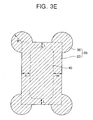
second pattern portions 30 are formed on the side surfaces of the portion including an apex on at least one side of thefirst pattern portion 20 such that portions of the second pattern portions are overlapped with the portion including an apex on at least one side of thefirst pattern portion 20. That is, thesecond pattern portion 30 is formed such that thesecond pattern portion 30 surrounds the portion including an apex on at least one side of thefirst pattern portion 20, wherein thesecond pattern portion 30 reinforced on the portion including an apex on at least one side of thefirst pattern portion 20 preferably has an area of 12 to 2,700 µm2. Although the adhesive force of a transfer layer separated from a receptor substrate and a donor substrate is increased, an opening defect can be formed on the portion including an apex on at least one side of thefirst pattern portion 20. Therefore, the opening defect can be completely prevented from being formed by further forming an extra reinforcement region on the portion including an apex on at least one side of thefirst pattern portion 20. - Since the same constitutional factors and reference numbers as in FIG. 3D are contained in FIG. 3E except that the second pattern portion is formed in a circular shape, a repeated description has been omitted.
- The
second pattern portion 30 is formed around an apex of thefirst pattern portion 20 in a circular shape such that a radius R of thesecond pattern portion 30 is L+H. That is, the radius R of the second pattern portion is from 4 to 60 µm, and thesecond pattern portion 30 has an area of 37 to 8,500 µm2 to increase the adhesive force of a transfer layer separated from a receptor substrate and a donor substrate accordingly. Furthermore, more uniformed patterns can be formed by reinforcing thesecond pattern portion 30 in a circular shape on respective regions of a portion including an apex on one side such that the second pattern portion has uniform length, thereby giving a uniform adhesive force to corners. - Although the
second pattern portion 30 is illustrated as a rectangular or circular shape in the drawings, the second pattern portion is not limited to the rectangular or circular shape since an organic layer pattern formed by the second pattern portion is a non-emitting region. - FIG. 4A to FIG. 4C are drawings for explaining an organic electroluminescent device fabrication method according to exemplary embodiments of the present invention.
- Referring to FIG. 4A, a
LITI device 100 includes alaser generator 110, aLITI mask 130 installed under thelaser generator 110, and aprojection lens 140; theLITI device 100 further includes a beam shaper, not illustrated in FIG. 4A, installed between thelaser generator 110 and theLITI mask 130 to cause auniform laser beam 111 to be irradiated from thelaser generator 110. - A
substrate 200 having a pixel electrode under theLITI device 100 is laminated with adonor substrate 250 having at least one transfer layer above thesubstrate 200. - Thereafter, a
laser beam 111 is produced by thelaser generator 110, and thelaser beam 111 passes through theLITI mask 130 that is patterned in a prescribed shape; thelaser beam 111 transmits a pattern group of theLITI mask 130 havingpatterns LITI mask 130. - The
laser beam 111 passing through theLITI mask 130 reaches the donor substrate by being transmitted through the projection lens. - A mosaic, delta or stripe shaped pattern is formed on an upper portion of the
substrate 200 according to shape of the LITI mask. - Therefore, a first pattern group a is completed on an upper portion of the
substrate 200 through the foregoing process. - After forming the first pattern group a, the LITI device is moved in a direction II, and the
mask 130 installed in the LITI device is moved a fixed distance in a transfer direction I. - Thereafter, the laser beam is patterned by transmitting the
laser beam 111 through a repeated pattern group of themask 130, and a second pattern group b is formed on an upper portion of thesubstrate 200 by irradiating the patterned laser beam onto an upper portion of thedonor substrate 250. - When the second pattern group b is formed on the upper portion of the
substrate 200, the LITI device is again moved in the direction II, and theLITI mask 130 installed in the LITI device is again moved a fixed distance in the transfer direction I. - Thereafter, the laser beam is patterned by transmitting the
laser beam 111 through a repeated pattern group of theLITI mask 130, and a third pattern group c is formed on an upper portion of thesubstrate 200 by irradiating the patterned laser beam onto an upper portion of thedonor substrate 250. - The foregoing process is capable of moving the stage and the
LITI mask 130 such that the movement of astage 300 along the substrate is synchronized with the movement of theLITI mask 130 or moving the stage and theLITI mask 130 while respective groups are being moved one step at a time. - An organic film, illustrated in the drawings, is patterned on an upper portion of the
substrate 200 when the transfer in the direction TT has been completed by repeating the foregoing process. - The organic layer pattern can be an emitting layer. The organic layer pattern further includes one or more layers selected from the group consisting of a hole injection layer, a hole transport layer, a hole inhibition layer and an electron injection layer.
- FIG. 4B and FIG. 4C are respective views of a donor substrate and a substrate laminated with a mask as perspective views for expanding one unit pixel A in FIG. 4A.
- Referring to FIG. 4B, the foregoing
LITI mask 130 includes afirst pattern portion 131, and asecond pattern portion 132 for reinforcing a portion including an apex on at least one side of thefirst pattern portion 131. - A
laser beam 111 is irradiated onto thedonor substrate 250 according to the shape of thefirst pattern portion 131 and thesecond pattern portion 132 of theLITI mask 130; thedonor substrate 250 includes at least asubstrate layer 260, a light to heatconversion layer 270 and atransfer layer 280. Furthermore, areceptor substrate 200 is laminated on a lower portion of thedonor substrate 250. Thereceptor substrate 200 includes asubstrate 210, apixel electrode 220 formed on thesubstrate 210, and apixel defining layer 230 formed on thepixel electrode 220 to define apixel portion 300. - The
laser beam 111 projected on thedonor substrate 250 is absorbed into the light to heatconversion layer 270 of thedonor substrate 250 such that thelaser beam 111 absorbed into the light to heatconversion layer 270 is converted into heat. The heat has an effect on thetransfer layer 280 such that the transfer layer is separated from thedonor substrate 250 and transferred onto thepixel electrode 220 of thereceptor substrate 200. - The transfer layer transferred onto the
pixel electrode 220 can come off a portion including an apex on one side due to a surface level difference of thereceptor substrate 200. Although an area of a transfer layer transferred onto the portion including an apex on one side can be decreased compared with area of a transfer layer transferred onto other regions, the area of a transfer layer transferred onto the portion including an apex on one side is not decreased by thesecond pattern 132 reinforced on a portion including an apex on at least one side of thefirst pattern portion 131 of the mask. - Thereafter, an adhesion area of a transfer layer transferred onto the portion including an apex on at least one side is increased during separation of the
receptor substrate 200 and thedonor substrate 250 to prevent an opening defect or uneven patterns from forming on a portion of thepixel electrode 220. - As illustrated in FIG. 4C, an organic layer 280' can be patterned and formed in a pattern shape of the mask on the
pixel electrode 220. That is, a first organic layer pattern portion 131' is formed by afirst pattern portion 131 in FIG. 4B of the mask. Furthermore, a second organic pattern portion 132' in which a portion including an apex on at least one side of the first organic layer pattern portion 131' is reinforced is formed by asecond pattern portion 132 in FIG. 4B of the mask; the second organic pattern portion 132' does not have an effect on an organic electroluminescent device since the second organic pattern portion 132' is formed on a non-emitting portion. - A transfer process of forming an organic layer pattern by the LITI device can be performed in a nitrogen atmosphere to prevent the organic layer pattern from being oxidized by oxygen existing in the atmosphere; it is preferable to charge nitrogen gas (N2) until an atmosphere containing 100 ppm of 02 and 100 ppm of H2O is created considering conditions in which the organic film is not influenced by oxygen or moisture since a considerable amount of time and money have to be invested to create a nitrogen atmosphere.
- Furthermore, the transfer process is performed in a vacuum atmosphere such that the generation of air bubbles between the donor substrate and the substrate can be suppressed during a process of laminating the donor substrate onto the front of the substrate.
- Subsequently, referring to FIG. 4A, an organic electroluminescent device is completed by forming patterns a, b and c of an organic film having certain cycles on an upper portion of a
substrate 200 and forming an upper electrode, not illustrated in FIG. 4A, on an upper portion of the organic layer pattern formedsubstrate 200. - Furthermore, an organic electroluminescent display device having an improved opening ratio can be fabricated by sealing the organic electroluminescent device.
- A laser irradiation apparatus according to the present embodiment may prevent a loss of picture quality due to the formation of opening defects and uneven organic layer patterns on a portion of the pixel portion by using a mask in which a portion including an apex on one side of mask pattern is reinforced.
- While the present invention has been particularly shown and described with reference to exemplary embodiments thereof, it will be understood by those skilled in the art that the foregoing and other modifications in form and detail can be made therein without departing from the scope of the present invention as defined by the following claims.
Claims (12)
- A Laser Induced Thermal Imaging, LITI, mask, comprising:a first pattern portion; anda second pattern portion arranged on at least one side of the first pattern portion and adjacent to an apex of the first pattern portion;wherein the second pattern portion has an area of between 8 and 8,500 µm2.
- A LITI mask according to claim 1, wherein the second pattern portion extends between 2 and 30 µm from the first pattern portion.
- A Laser Induced Thermal Imaging, LITI, mask, comprising:a first pattern portion; anda second pattern portion arranged on at least one side of the first pattern portion and adjacent to an apex of the first pattern portion;wherein the second pattern portion extends between 2 and 30 µm from the first pattern portion.
- A LITI mask according to any preceding claim, wherein the second pattern portion includes at least one portion having a width of between 4 and 60 µm.
- A LITI mask according to any preceding claim, wherein the second pattern portion surrounds the apex of the first pattern portion.
- A LITI mask according to any preceding claim, wherein the second pattern portion includes a portion having a curved shape.
- A LITI mask according to claim 6, wherein the second pattern portion includes a portion defined by part of a circle having a radius of between 4 and 60 µm and a centre substantially coinciding with the apex of the first pattern portion.
- A LITI mask according to any preceding claim, wherein the LITI mask is suitable for application to a LITI device equipped with an equal-magnification projection lens.
- A LITI mask according to any preceding claim, wherein the LITI mask has one of a stripe, mosaic or delta shape.
- A method of fabricating an organic electroluminescent device, comprising:forming a first electrode on a substrate;laminating a donor substrate onto an.upper portion of the first electrode formed on the substrate;forming an organic layer pattern by irradiating a laser beam passing through a Laser Induced Thermal Imaging, LITI, mask as claimed in any one of claims 1 to 9; andforming a second electrode on an upper portion of the organic layer pattern;wherein a reinforced region having an area of between 8 and 8,500 µm2 is formed on a portion arranged on at least one side of the organic layer pattern and adjacent to an apex of the organic layer pattern.
- A method according to claim 10, wherein the organic layer pattern is formed with a laser generator and a laser irradiation apparatus including an equal-magnification projection lens.
- A method according to claim 11, wherein the organic layer pattern is formed in a pattern shape of the LITI mask.
Applications Claiming Priority (1)
| Application Number | Priority Date | Filing Date | Title |
|---|---|---|---|
| KR1020050074364A KR100645534B1 (en) | 2005-08-12 | 2005-08-12 | Laser thermal transfer mask and manufacturing method of organic electroluminescent device using same |
Publications (2)
| Publication Number | Publication Date |
|---|---|
| EP1752306A1 true EP1752306A1 (en) | 2007-02-14 |
| EP1752306B1 EP1752306B1 (en) | 2009-02-11 |
Family
ID=37459313
Family Applications (1)
| Application Number | Title | Priority Date | Filing Date |
|---|---|---|---|
| EP06254231A Active EP1752306B1 (en) | 2005-08-12 | 2006-08-11 | Mask for laser-induced thermal imaging |
Country Status (6)
| Country | Link |
|---|---|
| US (1) | US7820340B2 (en) |
| EP (1) | EP1752306B1 (en) |
| JP (1) | JP2007053092A (en) |
| KR (1) | KR100645534B1 (en) |
| CN (1) | CN1955841B (en) |
| DE (1) | DE602006005111D1 (en) |
Cited By (2)
| Publication number | Priority date | Publication date | Assignee | Title |
|---|---|---|---|---|
| GB2459908A (en) * | 2008-04-25 | 2009-11-11 | Lg Display Co Ltd | Method of manufacturing an organic light emitting display |
| US8012298B2 (en) * | 2007-12-31 | 2011-09-06 | Lg Display Co., Ltd. | Manufacturing method for organic light emitting display |
Families Citing this family (8)
| Publication number | Priority date | Publication date | Assignee | Title |
|---|---|---|---|---|
| US7620476B2 (en) * | 2005-02-18 | 2009-11-17 | Irobot Corporation | Autonomous surface cleaning robot for dry cleaning |
| KR101563237B1 (en) * | 2007-06-01 | 2015-10-26 | 가부시키가이샤 한도오따이 에네루기 켄큐쇼 | Manufacturing apparatus and manufacturing method of light-emitting device |
| US20090130427A1 (en) * | 2007-10-22 | 2009-05-21 | The Regents Of The University Of California | Nanomaterial facilitated laser transfer |
| KR100908726B1 (en) | 2007-12-28 | 2009-07-22 | 삼성모바일디스플레이주식회사 | Apparatus for laser induced thermal imaging |
| WO2009154156A1 (en) * | 2008-06-16 | 2009-12-23 | 東レ株式会社 | Patterning method, device manufacturing method using the patterning method, and device |
| KR20120042144A (en) | 2010-10-22 | 2012-05-03 | 삼성모바일디스플레이주식회사 | Liti mask, laser irradiation device and method of forming organic light emitting device using the mask |
| JPWO2016047349A1 (en) * | 2014-09-25 | 2017-07-06 | コニカミノルタ株式会社 | Method for manufacturing organic electroluminescence element |
| KR102797541B1 (en) | 2019-04-17 | 2025-04-21 | 삼성디스플레이 주식회사 | Display apparatus and manufacturing method thoreof |
Citations (3)
| Publication number | Priority date | Publication date | Assignee | Title |
|---|---|---|---|---|
| US5707765A (en) * | 1996-05-28 | 1998-01-13 | Microunity Systems Engineering, Inc. | Photolithography mask using serifs and method thereof |
| US20050048295A1 (en) * | 2003-08-28 | 2005-03-03 | Samsung Sdi Co., Ltd. | Donor film for flat panel display and method of fabricating OLED using the same |
| US20050115503A1 (en) * | 2003-12-02 | 2005-06-02 | Nobuo Hagiwara | Deposition mask and manufacturing method thereof |
Family Cites Families (9)
| Publication number | Priority date | Publication date | Assignee | Title |
|---|---|---|---|---|
| JP2002222694A (en) | 2001-01-25 | 2002-08-09 | Sharp Corp | Laser processing apparatus and organic electroluminescent display panel using the same |
| KR100656490B1 (en) | 2001-11-26 | 2006-12-12 | 삼성에스디아이 주식회사 | Full color organic light emitting display device and manufacturing method thereof |
| JP2005202418A (en) | 2001-12-06 | 2005-07-28 | Seiko Epson Corp | Electro-optical device and electronic apparatus |
| US6810919B2 (en) | 2002-01-11 | 2004-11-02 | Seiko Epson Corporation | Manufacturing method for display device, display device, manufacturing method for electronic apparatus, and electronic apparatus |
| JP2003255508A (en) | 2002-02-28 | 2003-09-10 | Oki Electric Ind Co Ltd | Correction method for mask pattern, photomask, exposure method and semiconductor device |
| JP4519532B2 (en) | 2003-06-16 | 2010-08-04 | 株式会社半導体エネルギー研究所 | LIGHT EMITTING DEVICE AND ELECTRONIC DEVICE USING LIGHT EMITTING DEVICE |
| US7033711B2 (en) * | 2003-07-16 | 2006-04-25 | Eastman Kodak Company | Aperture ratio or resolution of an OLED device by limiting the edge taper region |
| JP2005085799A (en) | 2003-09-04 | 2005-03-31 | Seiko Epson Corp | Film forming method, wiring pattern forming method, semiconductor device manufacturing method, electro-optical device, and electronic apparatus |
| KR100667062B1 (en) | 2003-11-29 | 2007-01-10 | 삼성에스디아이 주식회사 | Donor substrate for laser transfer and organic electroluminescent element manufactured using the substrate |
-
2005
- 2005-08-12 KR KR1020050074364A patent/KR100645534B1/en not_active Expired - Lifetime
-
2006
- 2006-08-09 US US11/501,059 patent/US7820340B2/en active Active
- 2006-08-11 JP JP2006220703A patent/JP2007053092A/en active Pending
- 2006-08-11 DE DE602006005111T patent/DE602006005111D1/en active Active
- 2006-08-11 EP EP06254231A patent/EP1752306B1/en active Active
- 2006-08-14 CN CN2006101371428A patent/CN1955841B/en active Active
Patent Citations (3)
| Publication number | Priority date | Publication date | Assignee | Title |
|---|---|---|---|---|
| US5707765A (en) * | 1996-05-28 | 1998-01-13 | Microunity Systems Engineering, Inc. | Photolithography mask using serifs and method thereof |
| US20050048295A1 (en) * | 2003-08-28 | 2005-03-03 | Samsung Sdi Co., Ltd. | Donor film for flat panel display and method of fabricating OLED using the same |
| US20050115503A1 (en) * | 2003-12-02 | 2005-06-02 | Nobuo Hagiwara | Deposition mask and manufacturing method thereof |
Cited By (4)
| Publication number | Priority date | Publication date | Assignee | Title |
|---|---|---|---|---|
| US8012298B2 (en) * | 2007-12-31 | 2011-09-06 | Lg Display Co., Ltd. | Manufacturing method for organic light emitting display |
| GB2459908A (en) * | 2008-04-25 | 2009-11-11 | Lg Display Co Ltd | Method of manufacturing an organic light emitting display |
| GB2459908B (en) * | 2008-04-25 | 2011-03-09 | Lg Display Co Ltd | Method of manufacturing organic light emitting display |
| US7923284B2 (en) | 2008-04-25 | 2011-04-12 | Lg Display Co., Ltd. | Method of manufacturing organic light emitting display |
Also Published As
| Publication number | Publication date |
|---|---|
| JP2007053092A (en) | 2007-03-01 |
| KR100645534B1 (en) | 2006-11-14 |
| US7820340B2 (en) | 2010-10-26 |
| CN1955841B (en) | 2010-07-14 |
| EP1752306B1 (en) | 2009-02-11 |
| CN1955841A (en) | 2007-05-02 |
| US20070034866A1 (en) | 2007-02-15 |
| DE602006005111D1 (en) | 2009-03-26 |
Similar Documents
| Publication | Publication Date | Title |
|---|---|---|
| US7999835B2 (en) | Laser irradiation apparatus and method of fabricating organic light emitting display using the same | |
| KR101456023B1 (en) | Method of fabricating organic electro luminescent device | |
| US8741535B2 (en) | Laser irradiation device and method of fabricating organic light emitting display device using the same | |
| EP1752306B1 (en) | Mask for laser-induced thermal imaging | |
| JP4535387B2 (en) | Method for manufacturing donor substrate, and method for manufacturing organic electroluminescent display device using donor substrate | |
| US7686052B2 (en) | Lamination apparatus and laser-induced thermal imaging method using the same | |
| CN100448063C (en) | Laser irradiation device and method of manufacturing organic light emitting display using same | |
| KR20060020031A (en) | Laser thermal transfer device | |
| KR20180089606A (en) | The manufacturing method of the mask assembly | |
| EP1641055A1 (en) | Method for fabricating organic electroluminescence device | |
| KR20060020049A (en) | Laser thermal transfer method for manufacturing organic light emitting display device | |
| KR100959111B1 (en) | Manufacturing apparatus and manufacturing method of organic light emitting device | |
| KR100623698B1 (en) | Manufacturing method of donor substrate and manufacturing method of organic electroluminescent element using same | |
| KR100761073B1 (en) | Laser thermal transfer method | |
| KR100989137B1 (en) | Donor substrate for laser thermal transfer, manufacturing method thereof and manufacturing method of organic light emitting display device using the same | |
| KR100623705B1 (en) | Donor substrate manufacturing apparatus, donor substrate manufacturing method and organic light emitting display device manufacturing method using the donor substrate | |
| KR100812027B1 (en) | Laser thermal transfer device and manufacturing method of organic light emitting device using same | |
| KR100699992B1 (en) | Manufacturing method of laser transfer device and organic light emitting display device | |
| KR100796587B1 (en) | Manufacturing method of donor substrate and manufacturing method of organic electroluminescent element using same | |
| KR20060026790A (en) | Manufacturing method of organic electroluminescent element | |
| KR20060021215A (en) | Manufacturing method of donor substrate and manufacturing method of organic electroluminescent element using same | |
| KR20050082374A (en) | Donor film for plat panel display |
Legal Events
| Date | Code | Title | Description |
|---|---|---|---|
| PUAI | Public reference made under article 153(3) epc to a published international application that has entered the european phase |
Free format text: ORIGINAL CODE: 0009012 |
|
| 17P | Request for examination filed |
Effective date: 20060817 |
|
| AK | Designated contracting states |
Kind code of ref document: A1 Designated state(s): AT BE BG CH CY CZ DE DK EE ES FI FR GB GR HU IE IS IT LI LT LU LV MC NL PL PT RO SE SI SK TR |
|
| AX | Request for extension of the european patent |
Extension state: AL BA HR MK YU |
|
| RIN1 | Information on inventor provided before grant (corrected) |
Inventor name: KIM, JIN-SOOC/O SAMSUNG SDI CO., LTD. Inventor name: KANG, TAE-MINC/O LEGAL & IP TEAM CORP. PLANNING ST Inventor name: LEE, SEONG-TAEKC/O SAMSUNG SDI CO., LTD. Inventor name: LEE, JAE-HOC/O SAMSUNG SDI CO., LTD. |
|
| AKX | Designation fees paid |
Designated state(s): DE FR GB |
|
| GRAP | Despatch of communication of intention to grant a patent |
Free format text: ORIGINAL CODE: EPIDOSNIGR1 |
|
| GRAS | Grant fee paid |
Free format text: ORIGINAL CODE: EPIDOSNIGR3 |
|
| GRAA | (expected) grant |
Free format text: ORIGINAL CODE: 0009210 |
|
| AK | Designated contracting states |
Kind code of ref document: B1 Designated state(s): DE FR GB |
|
| REG | Reference to a national code |
Ref country code: GB Ref legal event code: FG4D |
|
| RAP2 | Party data changed (patent owner data changed or rights of a patent transferred) |
Owner name: SAMSUNG MOBILE DISPLAY CO., LTD. |
|
| REF | Corresponds to: |
Ref document number: 602006005111 Country of ref document: DE Date of ref document: 20090326 Kind code of ref document: P |
|
| REG | Reference to a national code |
Ref country code: DE Ref legal event code: R096 Ref document number: 602006005111 Country of ref document: DE Effective date: 20090326 |
|
| PLBE | No opposition filed within time limit |
Free format text: ORIGINAL CODE: 0009261 |
|
| STAA | Information on the status of an ep patent application or granted ep patent |
Free format text: STATUS: NO OPPOSITION FILED WITHIN TIME LIMIT |
|
| 26N | No opposition filed |
Effective date: 20091112 |
|
| REG | Reference to a national code |
Ref country code: DE Ref legal event code: R097 Ref document number: 602006005111 Country of ref document: DE Effective date: 20091112 |
|
| REG | Reference to a national code |
Ref country code: FR Ref legal event code: TP Owner name: SAMSUNG DISPLAY CO., LTD., KR Effective date: 20121226 |
|
| REG | Reference to a national code |
Ref country code: GB Ref legal event code: 732E Free format text: REGISTERED BETWEEN 20130103 AND 20130109 |
|
| REG | Reference to a national code |
Ref country code: DE Ref legal event code: R082 Ref document number: 602006005111 Country of ref document: DE Representative=s name: MARKS & CLERK (LUXEMBOURG) LLP, LU |
|
| REG | Reference to a national code |
Ref country code: DE Ref legal event code: R081 Ref document number: 602006005111 Country of ref document: DE Owner name: SAMSUNG DISPLAY CO., LTD., KR Free format text: FORMER OWNER: SAMSUNG SDI CO., LTD., SUWON, KR Effective date: 20130201 Ref country code: DE Ref legal event code: R082 Ref document number: 602006005111 Country of ref document: DE Representative=s name: MARKS & CLERK (LUXEMBOURG) LLP, LU Effective date: 20130201 Ref country code: DE Ref legal event code: R081 Ref document number: 602006005111 Country of ref document: DE Owner name: SAMSUNG DISPLAY CO., LTD., YONGIN-CITY, KR Free format text: FORMER OWNER: SAMSUNG SDI CO., LTD., SUWON, KYONGGI-DO, KR Effective date: 20130201 |
|
| REG | Reference to a national code |
Ref country code: FR Ref legal event code: PLFP Year of fee payment: 11 |
|
| REG | Reference to a national code |
Ref country code: FR Ref legal event code: PLFP Year of fee payment: 12 |
|
| REG | Reference to a national code |
Ref country code: FR Ref legal event code: PLFP Year of fee payment: 13 |
|
| P01 | Opt-out of the competence of the unified patent court (upc) registered |
Effective date: 20230515 |
|
| PGFP | Annual fee paid to national office [announced via postgrant information from national office to epo] |
Ref country code: DE Payment date: 20240722 Year of fee payment: 19 |
|
| PGFP | Annual fee paid to national office [announced via postgrant information from national office to epo] |
Ref country code: GB Payment date: 20240723 Year of fee payment: 19 |
|
| PGFP | Annual fee paid to national office [announced via postgrant information from national office to epo] |
Ref country code: FR Payment date: 20240723 Year of fee payment: 19 |
|
| REG | Reference to a national code |
Ref country code: DE Ref legal event code: R119 Ref document number: 602006005111 Country of ref document: DE |
|
| GBPC | Gb: european patent ceased through non-payment of renewal fee |
Effective date: 20250811 |