EP1748451B1 - Magnetic element - Google Patents
Magnetic element Download PDFInfo
- Publication number
- EP1748451B1 EP1748451B1 EP06015061A EP06015061A EP1748451B1 EP 1748451 B1 EP1748451 B1 EP 1748451B1 EP 06015061 A EP06015061 A EP 06015061A EP 06015061 A EP06015061 A EP 06015061A EP 1748451 B1 EP1748451 B1 EP 1748451B1
- Authority
- EP
- European Patent Office
- Prior art keywords
- flat plate
- magnetic
- magnetic material
- portions
- magnetic element
- Prior art date
- Legal status (The legal status is an assumption and is not a legal conclusion. Google has not performed a legal analysis and makes no representation as to the accuracy of the status listed.)
- Active
Links
- 239000000696 magnetic material Substances 0.000 claims abstract description 59
- 239000004020 conductor Substances 0.000 claims abstract description 40
- 238000009413 insulation Methods 0.000 claims description 5
- 239000000463 material Substances 0.000 claims description 5
- 239000000843 powder Substances 0.000 claims description 4
- 239000011347 resin Substances 0.000 claims description 4
- 229920005989 resin Polymers 0.000 claims description 4
- RYGMFSIKBFXOCR-UHFFFAOYSA-N Copper Chemical compound [Cu] RYGMFSIKBFXOCR-UHFFFAOYSA-N 0.000 description 5
- 229910052802 copper Inorganic materials 0.000 description 4
- 239000010949 copper Substances 0.000 description 4
- XEEYBQQBJWHFJM-UHFFFAOYSA-N Iron Chemical group [Fe] XEEYBQQBJWHFJM-UHFFFAOYSA-N 0.000 description 3
- 238000000576 coating method Methods 0.000 description 3
- 239000011162 core material Substances 0.000 description 3
- 230000012447 hatching Effects 0.000 description 3
- 238000004519 manufacturing process Methods 0.000 description 3
- 238000000034 method Methods 0.000 description 3
- 238000004804 winding Methods 0.000 description 3
- 229910000859 α-Fe Inorganic materials 0.000 description 3
- 239000011230 binding agent Substances 0.000 description 2
- 239000011889 copper foil Substances 0.000 description 2
- 238000005520 cutting process Methods 0.000 description 2
- 230000007423 decrease Effects 0.000 description 2
- 210000003298 dental enamel Anatomy 0.000 description 2
- 239000004744 fabric Substances 0.000 description 2
- 239000012774 insulation material Substances 0.000 description 2
- 230000004048 modification Effects 0.000 description 2
- 238000012986 modification Methods 0.000 description 2
- 239000004593 Epoxy Substances 0.000 description 1
- 239000004698 Polyethylene Substances 0.000 description 1
- 230000002411 adverse Effects 0.000 description 1
- 239000011248 coating agent Substances 0.000 description 1
- 150000001879 copper Chemical class 0.000 description 1
- 230000006866 deterioration Effects 0.000 description 1
- 239000002320 enamel (paints) Substances 0.000 description 1
- 229910052742 iron Inorganic materials 0.000 description 1
- 239000007788 liquid Substances 0.000 description 1
- 239000000203 mixture Substances 0.000 description 1
- -1 polyethylene Polymers 0.000 description 1
- 229920000573 polyethylene Polymers 0.000 description 1
- 238000004080 punching Methods 0.000 description 1
- 229920006305 unsaturated polyester Polymers 0.000 description 1
Images


Classifications
-
- H—ELECTRICITY
- H01—ELECTRIC ELEMENTS
- H01F—MAGNETS; INDUCTANCES; TRANSFORMERS; SELECTION OF MATERIALS FOR THEIR MAGNETIC PROPERTIES
- H01F17/00—Fixed inductances of the signal type
- H01F17/0006—Printed inductances
- H01F17/0033—Printed inductances with the coil helically wound around a magnetic core
-
- H—ELECTRICITY
- H01—ELECTRIC ELEMENTS
- H01F—MAGNETS; INDUCTANCES; TRANSFORMERS; SELECTION OF MATERIALS FOR THEIR MAGNETIC PROPERTIES
- H01F17/00—Fixed inductances of the signal type
- H01F17/04—Fixed inductances of the signal type with magnetic core
- H01F17/045—Fixed inductances of the signal type with magnetic core with core of cylindric geometry and coil wound along its longitudinal axis, i.e. rod or drum core
-
- H—ELECTRICITY
- H01—ELECTRIC ELEMENTS
- H01F—MAGNETS; INDUCTANCES; TRANSFORMERS; SELECTION OF MATERIALS FOR THEIR MAGNETIC PROPERTIES
- H01F17/00—Fixed inductances of the signal type
- H01F17/0006—Printed inductances
- H01F2017/0066—Printed inductances with a magnetic layer
-
- H—ELECTRICITY
- H01—ELECTRIC ELEMENTS
- H01F—MAGNETS; INDUCTANCES; TRANSFORMERS; SELECTION OF MATERIALS FOR THEIR MAGNETIC PROPERTIES
- H01F27/00—Details of transformers or inductances, in general
- H01F27/28—Coils; Windings; Conductive connections
- H01F27/2847—Sheets; Strips
-
- H—ELECTRICITY
- H01—ELECTRIC ELEMENTS
- H01F—MAGNETS; INDUCTANCES; TRANSFORMERS; SELECTION OF MATERIALS FOR THEIR MAGNETIC PROPERTIES
- H01F27/00—Details of transformers or inductances, in general
- H01F27/28—Coils; Windings; Conductive connections
- H01F27/30—Fastening or clamping coils, windings, or parts thereof together; Fastening or mounting coils or windings on core, casing, or other support
- H01F27/306—Fastening or mounting coils or windings on core, casing or other support
Definitions
- the present invention relates to a magnetic element.
- a typical structure of a conventionally-known magnetic element is a wound structure with a conductive wire being wound around the outer circumference of a columnar core material made of a magnetic material, as disclosed in, for example, Japanese Patent Application Laid-Open No. 2005-109181 .
- the core material needs a certain degree of thickness from the stand point of improvement of workability when winding the conductive wire. For this reason, there is a problem in that the thickness of the magnetic element becomes large and therefore it is difficult to secure an arrangement space when the magnetic element is arranged in electric appliances.
- JP 58 137206 A discloses an inductance element having a first rigid flat plate made of ferrite. Further, the inductance element has a second flat plate made of a flexible board provided with a zigzag pattern formed with copper foil.
- the first rigid flat plate can be introduced in the zigzag pattern of the second flat plate so as to alternately weave front and back surfaces of the second flat plate. Since the first flat plate is a rigid element, no variation of the shapes of the inductance element is possible. Every second winding of the copper foil gets in conducting touch with the ferrite core.
- US 2005/122200 A1 discloses an inductor coil and a method for making the same.
- the coil is made from a blank flat conductor plate made of rigid copper.
- the zigzag shape of the coil is then created by cutting out rectangular pieces from this copper plate.
- US 2,568,169 discloses a stamped helical coil, made of a rigid rectangular sheet made of conductive material.
- the rectangular sheet is formed with a series of transverse slots. Afterwards, the respective rectangular portions are spread away from each other, to form a coil.
- JP 60 009109 A discloses a transformer having a secondary winding made of a thick conductor bar which is turned once or several times through a spiral iron core.
- the present invention has been made in view of the above-described circumstance, and an object of the present invention is to provide a magnetic element an arrangement space of which can be reduced.
- the first flat plate and the second flat plate have flexibility. According to such a configuration, the whole magnetic element has flexibility.
- the second flat plate has the surface thereof coated with an insulation film. Such a configuration can reduce a risk in which any portion of the helical structure of the second flat plate is short-circuited.
- the magnetic element is made of the magnetic material formed by combining magnetic material powders with a resin material.
- the magnetic element includes the second flat plate that is alternatively slit from right and left sides in the width direction. Therefore, the first flat plate is inserted so that the slit portions of the second flat plate are sewn, whereby the magnetic element can be easily manufactured.
- the magnetic element in which both ends of the magnetic material are connected to constitute a closed magnetic path.
- an arrangement space of a magnetic element can be reduced.
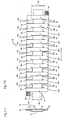
- FIG. 1 is a perspective view showing the entire configuration of a magnetic element according to an embodiment of the present invention.
- FIG. 2A and FIG. 2B are a front view and a plan view of the magnetic element according to the embodiment of the present invention.
- FIG. 3 is a left side view of the magnetic element according to the embodiment of the present invention.
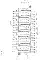
- FIG. 4 is a plan view of a conductive material according to the embodiment of the present invention.
- FIG. 5 is a view showing a manufacturing method of the conductive material according to the embodiment of the present invention.
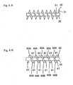
- FIG. 6A and FIG. 6B are front views, each showing a magnetic element according to a modification example of the present invention.
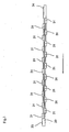
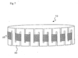
- FIG. 7 is a modification example of the magnetic element of the present invention and a view showing the magnetic element in which a closed magnetic path is formed by connecting both ends of a magnetic material.
- FIG. 1 is a perspective view showing the entire configuration of a magnetic element 10
- FIG. 2A is a front view of the magnetic element 10
- FIG. 2B is a plan view of the magnetic element 10.
- FIG. 3 is a left side view of the magnetic element 10.
- the magnetic element 10 has a magnetic material 20 as a first flat plate and a conductive material 30 as a second flat plate.
- the magnetic material 20 is formed by combining magnetic material powders such as ferrite and iron with a resin material such as polyethylene, unsaturated polyester, and epoxy as a binder, and is formed in a rectangular flat-plate shape. Since the magnetic material 20 is formed by combining the magnetic material powders with the resin material as the binder, it has flexibility and can be bent in the longitudinal and width directions.
- FIG. 4 is a plan view of the conductive material 30.
- the following will be described on the assumption that a direction shown by an arrow indicating a longitudinal direction of the magnetic material 20 is set as the front; a right side of the arrow direction is set as the right; and a left side of the arrow direction is set as the left.
- the conductive material 30 has flexible, thin plate-like, and rectangular strip-shaped portions 31 which are connected by connection portions 31A to present in a plate-like, helical shape as a whole. Furthermore, the conductive material 30 is composed of a conductive material such as copper. Then, as shown in FIG. 1 to FIG. 3 , the magnetic material 20 is inserted in the helical structure of the conductive material 30 so as to alternatively weave the front and back surfaces of the strip-shaped portions 31.
- each strip-shaped portion 31 is connected by the connection portion 31A to an adjacent strip-shaped portion 31, which is located in the front direction, on one side of the ends in the right-left direction, and the other of the ends of each strip-shaped portion 31 is connected by the connection portion 31A to an adjacent strip-shaped portion 31, which is located in the back direction, on the other side of the ends in the right-left direction. Therefore, the conductive material 30 has the connection portions 31A which serve as portions bent towards the right-left direction to present in a substantially zig-zag strip shape as a whole.
- a length of a portion 32A defined by overlapping, in the front-back direction, gap portions 32 with each other which are formed between the strip-shaped portions 31 arranged in parallel is formed to be wider than a width 20L of the magnetic material 20 in the right-left direction.
- the strip-shaped portions 31 have flexibility and therefore the whole conductive material 30 also has flexibility.
- the surface of the conductive material 30 is coated with an insulation material such as enamel except for terminal portions 33 and 34 (portions shown by hatching in FIG. 1 , FIG. 2 , and FIG. 4 ) which are formed at both ends in the front-back direction.
- the conductive material 30 is alternatively intersected with one surface and the other surface of the magnetic material 20, that is, the conductive material 30 is fitted so as to be intersected with respect to the magnetic material 20 at the front and back surfaces of the magnetic material 20.
- the magnetic material 20 passes through the portions 32A where the respective gap portions 32 overlap with each other in the front-back direction.
- the front surface of the drawing is set as the front surface of the magnetic material 20 and the back surface of the drawing is set as the back surface of the magnetic material 20 in FIG. 2 ; and in FIG. 1 and FIG. 3 , the upper side of the drawing is set as the front surface of the magnetic material 20 and the lower side of the drawing is set as the back surface of the magnetic material 20.
- the strip-shaped portions 31 intersecting with the magnetic material 20 in the conductive material 30 are alternately arranged on the front surface side of the magnetic material 20 and alternately arranged on the back surface side of the magnetic material 20, and consequently, the front and back surfaces of the magnetic material 20 are sandwiched by the strip-shaped portions 31.
- the conductive material 30 is fitted to the magnetic material 20, whereby it becomes the same configuration as that in which a conductive wire is wound around the magnetic material 20.
- the conductive material 30 of the first embodiment is manufactured in the following manner, for example.
- cutoff portions 40A and 40B shown by hatching are cut off by a punching process of a press, for example.
- the cutoff portions 40A are formed as slit portions which are formed from one edge extending in the longitudinal direction of the thin plate toward the other edge, however, a neighboring cutoff portion 40A is formed so that the slit direction thereof is oriented in the opposite direction and is provided so that connection portion 40C remains so as not to cut off the thin plate.
- Each of the cutoff portions 40B is provided at both ends in the longitudinal direction of the thin plate so that each of remaining portions 40D remains on the side from which the thin plate is slit to form the neighboring cutoff portion 40A.
- portions obtained by cutting off the cutoff portions 40A from the thin plate are formed as the gap portions 32.
- the connection portions 40C serve as the connection portions 31A.
- the remaining portions 40D are formed as the terminal portions 33 and 34.
- the conductive material 30 thus punched out from the thin plate is subjected to an insulation coating process by a method in which it is soaked in a tub filled with an insulation coating material such as enamel liquid or the like.
- the cutoff portion 40A is not shaped in such a manner that both sides of the slit portion come in contact with each other as in the case of being slit by scissors, for example, but is shaped with some widths being provided therebetween. Therefore, when the insulation coating process is performed, edge portions of the slit sides of the strip-shaped portions 31 are also completely coated with an insulation material.
- the enamel coating is scaled off to expose the conductive material.
- the magnetic material 20 is a linear flat plate and the conductive material 30 is a helical flat plate, and therefore, the magnetic element 10 is thinly formed as a whole. Therefore, when the magnetic element 10 is arranged in electric appliances and the like, limitation of arrangement space within the device is alleviated. Additionally, in this embodiment, both the magnetic material 20 and the conductive material 30 have flexibility and therefore the magnetic element 10 also has flexibility as a whole. Accordingly, the magnetic element 10 can be arranged along a shape such as an arrangement space or the like within the device and therefore limitation to the arrangement space or the like of the magnetic element 10 can be further alleviated.
- the conductive material 30 is fitted to the magnetic material 20 only by passing the magnetic material 20 through the gap portions 32; when manufacturing the magnetic element, a manufacturing step of the magnetic element can be simplified, as compared with a work that a conductive wire is wound around the magnetic material.
- the number of the cutoff portions 40A increases, the number of the strip-shaped portions 31 per length of the magnetic material 20, that is, the number of the strip-shaped portions 31 intersecting with the magnetic material 20 increases.
- the number of the slit portions decreases, the number of the strip-shaped portions 31 per length of the magnetic material 20 decreases. Therefore, the number of the cutoff portions 40A is suitably set and the number of the strip-shaped portions 31 per length of the magnetic material 20 is set, whereby an inductance value or the like of the magnetic element 10 can be suitably set.
- a sectional area or composition of the magnetic element 10 is suitably changed and an inductance value or the like can be also suitably set.
- both the magnetic material 20 serving as the first flat plate and the conductive material 30 serving as the second flat plate are allowed to have flexibility so that the magnetic element 10 has flexibility as a whole, however, it is sufficient if at least one of them has flexibility.
- the strip-shaped portions 31 cannot be alternatively arranged on the front and back surfaces of the magnetic material 20 while sandwiching the thickness of the magnetic material 20.
- the magnetic material 20 or the strip-shaped portions 31 are bent by as much as the thickness of the magnetic material 20, and as a result, the strip-shaped portions can be alternatively arranged on the front and back surfaces of the magnetic material 20.
- the first flat plate is made of a magnetic material and the second flat plate is made of a conductive material
- the first flat plate may be made of a conductive material and the second flat plate may be made of a magnetic material in an adverse manner.
- the magnetic element 10 thus configured is formed with the thickness thereof being thin and therefore it can be sewn into fabrics such as clothes. Furthermore, the flexibility of the magnetic element 10 allows for a minimum degree of deterioration in flexibility of fabric at a portion where the magnetic element 10 is sewn.
- a closed magnetic path is formed.
- another magnetic material 20 having the same shape as the magnetic material 20 is overlapped from above the strip-shaped portions of the conductive material 30, and if the both ends of the overlapping magnetic material 20 and the overlapped magnetic material 20 are connected, a thin magnetic element 10 forming a closed magnetic path can be constituted.
- the portion of the magnetic material 20 is shown by hatching in FIG. 7 . Furthermore, the details of the backside with respect to the drawing in FIG. 7 are omitted.
- the conductive material 30 may be formed to be a serration-type conductive material 50 in a zig-zag shape or a wave-type conductive material 60 in a zig-zag shape, as shown in FIG. 6A and 6B , respectively.
- straight portions 51 correspond to the strip-shaped portions 31 of the conductive material 30 shown in FIG. 1 to FIG. 5 .
- curved portions 61 connecting peak portions 60A and bottom portions 60B of the wave correspond to the strip-shaped portions 31 of the conductive material 30 shown in FIG. 1 to FIG. 5 .
- the magnetic element according to the present invention can be used in the field of magnetic elements such as inductors and antennas for use in RFID (Radio Frequency IDENTIFICATION).
Abstract
Description
- The present invention relates to a magnetic element.
- A typical structure of a conventionally-known magnetic element is a wound structure with a conductive wire being wound around the outer circumference of a columnar core material made of a magnetic material, as disclosed in, for example,
Japanese Patent Application Laid-Open No. 2005-109181 - Meanwhile, the core material needs a certain degree of thickness from the stand point of improvement of workability when winding the conductive wire. For this reason, there is a problem in that the thickness of the magnetic element becomes large and therefore it is difficult to secure an arrangement space when the magnetic element is arranged in electric appliances.
-
JP 58 137206 A -
US 2005/122200 A1 discloses an inductor coil and a method for making the same. The coil is made from a blank flat conductor plate made of rigid copper. The zigzag shape of the coil is then created by cutting out rectangular pieces from this copper plate. -
US 2,568,169 discloses a stamped helical coil, made of a rigid rectangular sheet made of conductive material. The rectangular sheet is formed with a series of transverse slots. Afterwards, the respective rectangular portions are spread away from each other, to form a coil. -
JP 60 009109 A - The present invention has been made in view of the above-described circumstance, and an object of the present invention is to provide a magnetic element an arrangement space of which can be reduced.
- The above mentioned problem is solved by a magnetic element having the features of
claim 1. - The first flat plate and the second flat plate have flexibility. According to such a configuration, the whole magnetic element has flexibility.
- According to the present invention, the second flat plate has the surface thereof coated with an insulation film. Such a configuration can reduce a risk in which any portion of the helical structure of the second flat plate is short-circuited.
- Furthermore, according to still another aspect of the present invention, the magnetic element is made of the magnetic material formed by combining magnetic material powders with a resin material.
- Furthermore, according to still another aspect of the present invention, the magnetic element includes the second flat plate that is alternatively slit from right and left sides in the width direction. Therefore, the first flat plate is inserted so that the slit portions of the second flat plate are sewn, whereby the magnetic element can be easily manufactured.
- Furthermore, according to still another aspect of the present invention, there is provided the magnetic element in which both ends of the magnetic material are connected to constitute a closed magnetic path.
- According to the present invention, an arrangement space of a magnetic element can be reduced.
-
FIG. 1 is a perspective view showing the entire configuration of a magnetic element according to an embodiment of the present invention. -
FIG. 2A and FIG. 2B are a front view and a plan view of the magnetic element according to the embodiment of the present invention. -
FIG. 3 is a left side view of the magnetic element according to the embodiment of the present invention. -
FIG. 4 is a plan view of a conductive material according to the embodiment of the present invention. -
FIG. 5 is a view showing a manufacturing method of the conductive material according to the embodiment of the present invention. -
FIG. 6A and FIG. 6B are front views, each showing a magnetic element according to a modification example of the present invention. - .
FIG. 7 is a modification example of the magnetic element of the present invention and a view showing the magnetic element in which a closed magnetic path is formed by connecting both ends of a magnetic material. - A magnetic element according to an embodiment of the present invention will be described below on the basis of
FIG. 1 to FIG. 4 .FIG. 1 is a perspective view showing the entire configuration of amagnetic element 10;FIG. 2A is a front view of themagnetic element 10; andFIG. 2B is a plan view of themagnetic element 10. Furthermore,FIG. 3 is a left side view of themagnetic element 10. - As shown in
FIG. 1 to FIG. 3 , themagnetic element 10 has amagnetic material 20 as a first flat plate and aconductive material 30 as a second flat plate. - First, the
magnetic material 20 will be described. Themagnetic material 20 is formed by combining magnetic material powders such as ferrite and iron with a resin material such as polyethylene, unsaturated polyester, and epoxy as a binder, and is formed in a rectangular flat-plate shape. Since themagnetic material 20 is formed by combining the magnetic material powders with the resin material as the binder, it has flexibility and can be bent in the longitudinal and width directions. - Next, the configuration of the
conductive material 30 will be described with reference toFIG. 1 to FIG. 4 .FIG. 4 is a plan view of theconductive material 30. InFIG. 1 to FIG. 4 , the following will be described on the assumption that a direction shown by an arrow indicating a longitudinal direction of themagnetic material 20 is set as the front; a right side of the arrow direction is set as the right; and a left side of the arrow direction is set as the left. - The
conductive material 30 has flexible, thin plate-like, and rectangular strip-shaped portions 31 which are connected byconnection portions 31A to present in a plate-like, helical shape as a whole. Furthermore, theconductive material 30 is composed of a conductive material such as copper. Then, as shown inFIG. 1 to FIG. 3 , themagnetic material 20 is inserted in the helical structure of theconductive material 30 so as to alternatively weave the front and back surfaces of the strip-shaped portions 31. - More specifically, one of ends of each strip-
shaped portion 31 is connected by theconnection portion 31A to an adjacent strip-shaped portion 31, which is located in the front direction, on one side of the ends in the right-left direction, and the other of the ends of each strip-shaped portion 31 is connected by theconnection portion 31A to an adjacent strip-shaped portion 31, which is located in the back direction, on the other side of the ends in the right-left direction. Therefore, theconductive material 30 has theconnection portions 31A which serve as portions bent towards the right-left direction to present in a substantially zig-zag strip shape as a whole. Furthermore, a length of a portion 32A defined by overlapping, in the front-back direction,gap portions 32 with each other which are formed between the strip-shaped portions 31 arranged in parallel is formed to be wider than a width 20L of themagnetic material 20 in the right-left direction. - Furthermore, the strip-
shaped portions 31 have flexibility and therefore the wholeconductive material 30 also has flexibility. In addition, the surface of theconductive material 30 is coated with an insulation material such as enamel except forterminal portions 33 and 34 (portions shown by hatching inFIG. 1 ,FIG. 2 , andFIG. 4 ) which are formed at both ends in the front-back direction. - The
conductive material 30 is alternatively intersected with one surface and the other surface of themagnetic material 20, that is, theconductive material 30 is fitted so as to be intersected with respect to themagnetic material 20 at the front and back surfaces of themagnetic material 20. In other words, themagnetic material 20 passes through the portions 32A where therespective gap portions 32 overlap with each other in the front-back direction. In addition, the front surface of the drawing is set as the front surface of themagnetic material 20 and the back surface of the drawing is set as the back surface of themagnetic material 20 inFIG. 2 ; and inFIG. 1 andFIG. 3 , the upper side of the drawing is set as the front surface of themagnetic material 20 and the lower side of the drawing is set as the back surface of themagnetic material 20. Therefore, the strip-shapedportions 31 intersecting with themagnetic material 20 in theconductive material 30 are alternately arranged on the front surface side of themagnetic material 20 and alternately arranged on the back surface side of themagnetic material 20, and consequently, the front and back surfaces of themagnetic material 20 are sandwiched by the strip-shapedportions 31. Thus, theconductive material 30 is fitted to themagnetic material 20, whereby it becomes the same configuration as that in which a conductive wire is wound around themagnetic material 20. - By the way, the
conductive material 30 of the first embodiment is manufactured in the following manner, for example. - First, with respect to a rectangular thin plate made of copper as shown in
FIG. 5 ,cutoff portions - The
cutoff portions 40A are formed as slit portions which are formed from one edge extending in the longitudinal direction of the thin plate toward the other edge, however, a neighboringcutoff portion 40A is formed so that the slit direction thereof is oriented in the opposite direction and is provided so thatconnection portion 40C remains so as not to cut off the thin plate. - Each of the
cutoff portions 40B is provided at both ends in the longitudinal direction of the thin plate so that each of remainingportions 40D remains on the side from which the thin plate is slit to form the neighboringcutoff portion 40A. - As described above, by providing the
cutoff portions 40A,cutoff portions 40B,connection portions 40C, and remainingportions 40D, portions obtained by cutting off thecutoff portions 40A from the thin plate are formed as thegap portions 32. Furthermore, theconnection portions 40C serve as theconnection portions 31A. Further, the remainingportions 40D are formed as theterminal portions - The
conductive material 30 thus punched out from the thin plate is subjected to an insulation coating process by a method in which it is soaked in a tub filled with an insulation coating material such as enamel liquid or the like. Thecutoff portion 40A is not shaped in such a manner that both sides of the slit portion come in contact with each other as in the case of being slit by scissors, for example, but is shaped with some widths being provided therebetween. Therefore, when the insulation coating process is performed, edge portions of the slit sides of the strip-shapedportions 31 are also completely coated with an insulation material. As for theterminal portions - As described above, the
magnetic material 20 is a linear flat plate and theconductive material 30 is a helical flat plate, and therefore, themagnetic element 10 is thinly formed as a whole. Therefore, when themagnetic element 10 is arranged in electric appliances and the like, limitation of arrangement space within the device is alleviated. Additionally, in this embodiment, both themagnetic material 20 and theconductive material 30 have flexibility and therefore themagnetic element 10 also has flexibility as a whole. Accordingly, themagnetic element 10 can be arranged along a shape such as an arrangement space or the like within the device and therefore limitation to the arrangement space or the like of themagnetic element 10 can be further alleviated. - Furthermore, since the
conductive material 30 is fitted to themagnetic material 20 only by passing themagnetic material 20 through thegap portions 32; when manufacturing the magnetic element, a manufacturing step of the magnetic element can be simplified, as compared with a work that a conductive wire is wound around the magnetic material. - In addition, when the number of the
cutoff portions 40A increases, the number of the strip-shapedportions 31 per length of themagnetic material 20, that is, the number of the strip-shapedportions 31 intersecting with themagnetic material 20 increases. On the other hand, when the number of the slit portions decreases, the number of the strip-shapedportions 31 per length of themagnetic material 20 decreases. Therefore, the number of thecutoff portions 40A is suitably set and the number of the strip-shapedportions 31 per length of themagnetic material 20 is set, whereby an inductance value or the like of themagnetic element 10 can be suitably set. Furthermore, a sectional area or composition of themagnetic element 10 is suitably changed and an inductance value or the like can be also suitably set. - In addition, in this embodiment, both the
magnetic material 20 serving as the first flat plate and theconductive material 30 serving as the second flat plate are allowed to have flexibility so that themagnetic element 10 has flexibility as a whole, however, it is sufficient if at least one of them has flexibility. This is because if none of them has flexibility, the strip-shapedportions 31 cannot be alternatively arranged on the front and back surfaces of themagnetic material 20 while sandwiching the thickness of themagnetic material 20. In other words, themagnetic material 20 or the strip-shapedportions 31 are bent by as much as the thickness of themagnetic material 20, and as a result, the strip-shaped portions can be alternatively arranged on the front and back surfaces of themagnetic material 20. - Furthermore, in this embodiment, the first flat plate is made of a magnetic material and the second flat plate is made of a conductive material, however, the first flat plate may be made of a conductive material and the second flat plate may be made of a magnetic material in an adverse manner.
- The
magnetic element 10 thus configured is formed with the thickness thereof being thin and therefore it can be sewn into fabrics such as clothes. Furthermore, the flexibility of themagnetic element 10 allows for a minimum degree of deterioration in flexibility of fabric at a portion where themagnetic element 10 is sewn. - Furthermore, as shown in
FIG. 7 , if the both ends of themagnetic material 20 are short-circuited or magnetically connected by U-shapedmagnetic material 20, a closed magnetic path is formed. For example, anothermagnetic material 20 having the same shape as themagnetic material 20 is overlapped from above the strip-shaped portions of theconductive material 30, and if the both ends of the overlappingmagnetic material 20 and the overlappedmagnetic material 20 are connected, a thinmagnetic element 10 forming a closed magnetic path can be constituted. The portion of themagnetic material 20 is shown by hatching inFIG. 7 . Furthermore, the details of the backside with respect to the drawing inFIG. 7 are omitted. - Furthermore, the
conductive material 30 may be formed to be a serration-typeconductive material 50 in a zig-zag shape or a wave-typeconductive material 60 in a zig-zag shape, as shown inFIG. 6A and 6B , respectively. It should be noted that in theconductive material 50,straight portions 51 correspond to the strip-shapedportions 31 of theconductive material 30 shown inFIG. 1 to FIG. 5 . Furthermore, in theconductive material 60,curved portions 61 connectingpeak portions 60A andbottom portions 60B of the wave correspond to the strip-shapedportions 31 of theconductive material 30 shown inFIG. 1 to FIG. 5 . - The magnetic element according to the present invention can be used in the field of magnetic elements such as inductors and antennas for use in RFID (Radio Frequency IDENTIFICATION).
Claims (4)
- A magnetic element (10) in a flat-plate shape, comprising:a linearly-extending first flat plate (20); anda helical second flat plate (30); whereinthe first flat plate (20) is made of a magnetic material and the second flat plate (30) is made of a conductive material; or the first flat plate (20) is made of a conductive material and the second flat plate (30) is made of a magnetic material;whereinthe first flat plate (20) is inserted into the helical structure of the second flat plate (30) so as to alternately weave front and back surfaces of the second flat plate (30),the first flat plate (20) and the second flat plate (30) have flexibility, andthe second flat plate (30) has the surface thereof coated with an insulation film.
- The magnetic element according to claim 1, wherein
the magnetic material is formed by combining magnetic material powders with a resin material. - The magnetic element according to claim 1 or 2, wherein
the second flat plate (30) is alternately slit from right and left sides in the width direction. - The magnetic element according to claim 1 or 2, wherein
the magnetic material has both ends thereof connected to constitute a closed magnetic path.
Applications Claiming Priority (1)
| Application Number | Priority Date | Filing Date | Title |
|---|---|---|---|
| JP2005216363A JP4825465B2 (en) | 2005-07-26 | 2005-07-26 | Magnetic element |
Publications (2)
| Publication Number | Publication Date |
|---|---|
| EP1748451A1 EP1748451A1 (en) | 2007-01-31 |
| EP1748451B1 true EP1748451B1 (en) | 2010-01-13 |
Family
ID=37085754
Family Applications (1)
| Application Number | Title | Priority Date | Filing Date |
|---|---|---|---|
| EP06015061A Active EP1748451B1 (en) | 2005-07-26 | 2006-07-19 | Magnetic element |
Country Status (6)
| Country | Link |
|---|---|
| US (1) | US7368908B2 (en) |
| EP (1) | EP1748451B1 (en) |
| JP (1) | JP4825465B2 (en) |
| CN (1) | CN100573754C (en) |
| AT (1) | ATE455353T1 (en) |
| DE (1) | DE602006011683D1 (en) |
Families Citing this family (8)
| Publication number | Priority date | Publication date | Assignee | Title |
|---|---|---|---|---|
| JP2007287830A (en) * | 2006-04-14 | 2007-11-01 | Sumida Corporation | Magnetic element |
| US8217748B2 (en) * | 2007-11-23 | 2012-07-10 | Alpha & Omega Semiconductor Inc. | Compact inductive power electronics package |
| US7868431B2 (en) * | 2007-11-23 | 2011-01-11 | Alpha And Omega Semiconductor Incorporated | Compact power semiconductor package and method with stacked inductor and integrated circuit die |
| US7884696B2 (en) * | 2007-11-23 | 2011-02-08 | Alpha And Omega Semiconductor Incorporated | Lead frame-based discrete power inductor |
| US7884452B2 (en) | 2007-11-23 | 2011-02-08 | Alpha And Omega Semiconductor Incorporated | Semiconductor power device package having a lead frame-based integrated inductor |
| CN104282418A (en) * | 2013-07-09 | 2015-01-14 | 善元科技股份有限公司 | Winding assembly for transformer device and transformer device |
| JP2015115448A (en) * | 2013-12-11 | 2015-06-22 | アイシン精機株式会社 | Inductor |
| CN104952596A (en) * | 2015-06-22 | 2015-09-30 | 广东明路电力电子有限公司 | Panel coil reactance or inductor and machining technology thereof |
Family Cites Families (19)
| Publication number | Priority date | Publication date | Assignee | Title |
|---|---|---|---|---|
| US3305814A (en) * | 1967-02-21 | Hybrid solid state device | ||
| US2568169A (en) * | 1949-05-11 | 1951-09-18 | Zenith Radio Corp | Stamped helical coil |
| US3413716A (en) * | 1965-04-30 | 1968-12-03 | Xerox Corp | Thin-film inductor elements |
| US3614554A (en) * | 1968-10-24 | 1971-10-19 | Texas Instruments Inc | Miniaturized thin film inductors for use in integrated circuits |
| US3858138A (en) * | 1973-03-05 | 1974-12-31 | Rca Corp | Tuneable thin film inductor |
| JPS5640209A (en) * | 1979-09-11 | 1981-04-16 | Inaba Denko Kk | Electromagnetic coil |
| JPS58137206A (en) * | 1982-02-09 | 1983-08-15 | Sony Corp | Inductance element |
| JPS6015905A (en) * | 1983-07-07 | 1985-01-26 | Murata Mfg Co Ltd | Inductive parts |
| JPS61117216A (en) * | 1984-11-12 | 1986-06-04 | Nippon Steel Corp | Manufacture of grain oriented magnetic steel plate of ultralow iron loss |
| JPH01107106A (en) * | 1987-10-21 | 1989-04-25 | Komatsu Ltd | Posture detector |
| US5392020A (en) * | 1992-12-14 | 1995-02-21 | Chang; Kern K. N. | Flexible transformer apparatus particularly adapted for high voltage operation |
| JP3422000B2 (en) * | 1993-09-17 | 2003-06-30 | 株式会社リコー | Wire loop, method for manufacturing wire loop, and method for manufacturing transformer |
| JPH07220932A (en) * | 1994-02-04 | 1995-08-18 | Mitsubishi Electric Corp | Coil element and its module |
| US5576680A (en) * | 1994-03-01 | 1996-11-19 | Amer-Soi | Structure and fabrication process of inductors on semiconductor chip |
| US7034645B2 (en) * | 1999-03-16 | 2006-04-25 | Vishay Dale Electronics, Inc. | Inductor coil and method for making same |
| JPH11261325A (en) * | 1998-03-10 | 1999-09-24 | Shiro Sugimura | Coil element and its manufacture |
| JP2002117383A (en) * | 2000-08-01 | 2002-04-19 | Mitsubishi Materials Corp | Antenna coil for rfid and its manufacturing method |
| JP2002164218A (en) * | 2000-11-29 | 2002-06-07 | Tokin Corp | Closed magnetic circuit thin-film inductor and its manufacturing method |
| JP2005109181A (en) | 2003-09-30 | 2005-04-21 | Tdk Corp | Coil-type electronic component |
-
2005
- 2005-07-26 JP JP2005216363A patent/JP4825465B2/en active Active
-
2006
- 2006-07-18 CN CNB2006101055577A patent/CN100573754C/en active Active
- 2006-07-19 AT AT06015061T patent/ATE455353T1/en not_active IP Right Cessation
- 2006-07-19 EP EP06015061A patent/EP1748451B1/en active Active
- 2006-07-19 DE DE602006011683T patent/DE602006011683D1/en active Active
- 2006-07-26 US US11/460,110 patent/US7368908B2/en active Active
Also Published As
| Publication number | Publication date |
|---|---|
| US20070024279A1 (en) | 2007-02-01 |
| US7368908B2 (en) | 2008-05-06 |
| JP2007035879A (en) | 2007-02-08 |
| CN1905092A (en) | 2007-01-31 |
| EP1748451A1 (en) | 2007-01-31 |
| DE602006011683D1 (en) | 2010-03-04 |
| CN100573754C (en) | 2009-12-23 |
| ATE455353T1 (en) | 2010-01-15 |
| JP4825465B2 (en) | 2011-11-30 |
Similar Documents
| Publication | Publication Date | Title |
|---|---|---|
| EP1748451B1 (en) | Magnetic element | |
| TWI789230B (en) | Inductor having high current coil with low direct current resistance | |
| US8910373B2 (en) | Method of manufacturing an electromagnetic component | |
| US8847831B2 (en) | Antenna and antenna module | |
| US20020093413A1 (en) | Inductor, transformer and manufacturing method thereof | |
| US20100001823A1 (en) | Flexible Coil | |
| EP0693733A1 (en) | Short-distance communication antennas and methods of manufacture and use of same | |
| DE102010035388A1 (en) | Inductor and DC-DC converter | |
| CN102099878A (en) | Sheet transformer for DC/DC converter | |
| US20190341692A1 (en) | Antenna device and electronic appliance | |
| JP2007035879A5 (en) | ||
| US6344784B1 (en) | Coil component | |
| JP6965858B2 (en) | Surface Mount Inductors and Their Manufacturing Methods | |
| US20180158593A1 (en) | Methods of forming coils for inductive components | |
| US20200136253A1 (en) | Antenna device and electronic apparatus | |
| JP3391596B2 (en) | Wires and transformers | |
| TWI810628B (en) | Method for manufacturing electronic component | |
| KR102095180B1 (en) | Plate coil and manufacture method thereof | |
| JP2017220849A (en) | Antenna device | |
| JP2003142323A (en) | Sheet coil and sheet transformer | |
| JP3623720B2 (en) | Thin inductor | |
| CN211929254U (en) | Winding assembly and magnetic assembly | |
| KR101927953B1 (en) | Antenna module and portable device having the same | |
| JPH10144528A (en) | Inductor and transformer using the inductor | |
| EP0978852A1 (en) | Multilayer type chip inductor |
Legal Events
| Date | Code | Title | Description |
|---|---|---|---|
| PUAI | Public reference made under article 153(3) epc to a published international application that has entered the european phase |
Free format text: ORIGINAL CODE: 0009012 |
|
| AK | Designated contracting states |
Kind code of ref document: A1 Designated state(s): AT BE BG CH CY CZ DE DK EE ES FI FR GB GR HU IE IS IT LI LT LU LV MC NL PL PT RO SE SI SK TR |
|
| AX | Request for extension of the european patent |
Extension state: AL BA HR MK YU |
|
| 17P | Request for examination filed |
Effective date: 20070605 |
|
| 17Q | First examination report despatched |
Effective date: 20070718 |
|
| AKX | Designation fees paid |
Designated state(s): AT BE BG CH CY CZ DE DK EE ES FI FR GB GR HU IE IS IT LI LT LU LV MC NL PL PT RO SE SI SK TR |
|
| GRAP | Despatch of communication of intention to grant a patent |
Free format text: ORIGINAL CODE: EPIDOSNIGR1 |
|
| GRAS | Grant fee paid |
Free format text: ORIGINAL CODE: EPIDOSNIGR3 |
|
| GRAA | (expected) grant |
Free format text: ORIGINAL CODE: 0009210 |
|
| AK | Designated contracting states |
Kind code of ref document: B1 Designated state(s): AT BE BG CH CY CZ DE DK EE ES FI FR GB GR HU IE IS IT LI LT LU LV MC NL PL PT RO SE SI SK TR |
|
| REG | Reference to a national code |
Ref country code: GB Ref legal event code: FG4D |
|
| REG | Reference to a national code |
Ref country code: CH Ref legal event code: EP |
|
| REG | Reference to a national code |
Ref country code: IE Ref legal event code: FG4D |
|
| REF | Corresponds to: |
Ref document number: 602006011683 Country of ref document: DE Date of ref document: 20100304 Kind code of ref document: P |
|
| REG | Reference to a national code |
Ref country code: NL Ref legal event code: VDEP Effective date: 20100113 |
|
| LTIE | Lt: invalidation of european patent or patent extension |
Effective date: 20100113 |
|
| PG25 | Lapsed in a contracting state [announced via postgrant information from national office to epo] |
Ref country code: AT Free format text: LAPSE BECAUSE OF FAILURE TO SUBMIT A TRANSLATION OF THE DESCRIPTION OR TO PAY THE FEE WITHIN THE PRESCRIBED TIME-LIMIT Effective date: 20100113 |
|
| PG25 | Lapsed in a contracting state [announced via postgrant information from national office to epo] |
Ref country code: NL Free format text: LAPSE BECAUSE OF FAILURE TO SUBMIT A TRANSLATION OF THE DESCRIPTION OR TO PAY THE FEE WITHIN THE PRESCRIBED TIME-LIMIT Effective date: 20100113 Ref country code: LT Free format text: LAPSE BECAUSE OF FAILURE TO SUBMIT A TRANSLATION OF THE DESCRIPTION OR TO PAY THE FEE WITHIN THE PRESCRIBED TIME-LIMIT Effective date: 20100113 Ref country code: IS Free format text: LAPSE BECAUSE OF FAILURE TO SUBMIT A TRANSLATION OF THE DESCRIPTION OR TO PAY THE FEE WITHIN THE PRESCRIBED TIME-LIMIT Effective date: 20100513 Ref country code: ES Free format text: LAPSE BECAUSE OF FAILURE TO SUBMIT A TRANSLATION OF THE DESCRIPTION OR TO PAY THE FEE WITHIN THE PRESCRIBED TIME-LIMIT Effective date: 20100424 Ref country code: PT Free format text: LAPSE BECAUSE OF FAILURE TO SUBMIT A TRANSLATION OF THE DESCRIPTION OR TO PAY THE FEE WITHIN THE PRESCRIBED TIME-LIMIT Effective date: 20100513 |
|
| PG25 | Lapsed in a contracting state [announced via postgrant information from national office to epo] |
Ref country code: PL Free format text: LAPSE BECAUSE OF FAILURE TO SUBMIT A TRANSLATION OF THE DESCRIPTION OR TO PAY THE FEE WITHIN THE PRESCRIBED TIME-LIMIT Effective date: 20100113 Ref country code: SI Free format text: LAPSE BECAUSE OF FAILURE TO SUBMIT A TRANSLATION OF THE DESCRIPTION OR TO PAY THE FEE WITHIN THE PRESCRIBED TIME-LIMIT Effective date: 20100113 Ref country code: FI Free format text: LAPSE BECAUSE OF FAILURE TO SUBMIT A TRANSLATION OF THE DESCRIPTION OR TO PAY THE FEE WITHIN THE PRESCRIBED TIME-LIMIT Effective date: 20100113 Ref country code: LV Free format text: LAPSE BECAUSE OF FAILURE TO SUBMIT A TRANSLATION OF THE DESCRIPTION OR TO PAY THE FEE WITHIN THE PRESCRIBED TIME-LIMIT Effective date: 20100113 |
|
| PG25 | Lapsed in a contracting state [announced via postgrant information from national office to epo] |
Ref country code: SE Free format text: LAPSE BECAUSE OF FAILURE TO SUBMIT A TRANSLATION OF THE DESCRIPTION OR TO PAY THE FEE WITHIN THE PRESCRIBED TIME-LIMIT Effective date: 20100113 Ref country code: GR Free format text: LAPSE BECAUSE OF FAILURE TO SUBMIT A TRANSLATION OF THE DESCRIPTION OR TO PAY THE FEE WITHIN THE PRESCRIBED TIME-LIMIT Effective date: 20100414 Ref country code: EE Free format text: LAPSE BECAUSE OF FAILURE TO SUBMIT A TRANSLATION OF THE DESCRIPTION OR TO PAY THE FEE WITHIN THE PRESCRIBED TIME-LIMIT Effective date: 20100113 Ref country code: CY Free format text: LAPSE BECAUSE OF FAILURE TO SUBMIT A TRANSLATION OF THE DESCRIPTION OR TO PAY THE FEE WITHIN THE PRESCRIBED TIME-LIMIT Effective date: 20100113 Ref country code: BE Free format text: LAPSE BECAUSE OF FAILURE TO SUBMIT A TRANSLATION OF THE DESCRIPTION OR TO PAY THE FEE WITHIN THE PRESCRIBED TIME-LIMIT Effective date: 20100113 Ref country code: RO Free format text: LAPSE BECAUSE OF FAILURE TO SUBMIT A TRANSLATION OF THE DESCRIPTION OR TO PAY THE FEE WITHIN THE PRESCRIBED TIME-LIMIT Effective date: 20100113 |
|
| PLBE | No opposition filed within time limit |
Free format text: ORIGINAL CODE: 0009261 |
|
| STAA | Information on the status of an ep patent application or granted ep patent |
Free format text: STATUS: NO OPPOSITION FILED WITHIN TIME LIMIT |
|
| PG25 | Lapsed in a contracting state [announced via postgrant information from national office to epo] |
Ref country code: SK Free format text: LAPSE BECAUSE OF FAILURE TO SUBMIT A TRANSLATION OF THE DESCRIPTION OR TO PAY THE FEE WITHIN THE PRESCRIBED TIME-LIMIT Effective date: 20100113 Ref country code: CZ Free format text: LAPSE BECAUSE OF FAILURE TO SUBMIT A TRANSLATION OF THE DESCRIPTION OR TO PAY THE FEE WITHIN THE PRESCRIBED TIME-LIMIT Effective date: 20100113 Ref country code: BG Free format text: LAPSE BECAUSE OF FAILURE TO SUBMIT A TRANSLATION OF THE DESCRIPTION OR TO PAY THE FEE WITHIN THE PRESCRIBED TIME-LIMIT Effective date: 20100413 |
|
| 26N | No opposition filed |
Effective date: 20101014 |
|
| PG25 | Lapsed in a contracting state [announced via postgrant information from national office to epo] |
Ref country code: DK Free format text: LAPSE BECAUSE OF FAILURE TO SUBMIT A TRANSLATION OF THE DESCRIPTION OR TO PAY THE FEE WITHIN THE PRESCRIBED TIME-LIMIT Effective date: 20100113 |
|
| PG25 | Lapsed in a contracting state [announced via postgrant information from national office to epo] |
Ref country code: MC Free format text: LAPSE BECAUSE OF NON-PAYMENT OF DUE FEES Effective date: 20100731 |
|
| REG | Reference to a national code |
Ref country code: CH Ref legal event code: PL |
|
| PG25 | Lapsed in a contracting state [announced via postgrant information from national office to epo] |
Ref country code: IT Free format text: LAPSE BECAUSE OF FAILURE TO SUBMIT A TRANSLATION OF THE DESCRIPTION OR TO PAY THE FEE WITHIN THE PRESCRIBED TIME-LIMIT Effective date: 20100113 |
|
| PG25 | Lapsed in a contracting state [announced via postgrant information from national office to epo] |
Ref country code: LI Free format text: LAPSE BECAUSE OF NON-PAYMENT OF DUE FEES Effective date: 20100731 Ref country code: CH Free format text: LAPSE BECAUSE OF NON-PAYMENT OF DUE FEES Effective date: 20100731 |
|
| PG25 | Lapsed in a contracting state [announced via postgrant information from national office to epo] |
Ref country code: IE Free format text: LAPSE BECAUSE OF NON-PAYMENT OF DUE FEES Effective date: 20100719 |
|
| PG25 | Lapsed in a contracting state [announced via postgrant information from national office to epo] |
Ref country code: LU Free format text: LAPSE BECAUSE OF NON-PAYMENT OF DUE FEES Effective date: 20100719 Ref country code: HU Free format text: LAPSE BECAUSE OF FAILURE TO SUBMIT A TRANSLATION OF THE DESCRIPTION OR TO PAY THE FEE WITHIN THE PRESCRIBED TIME-LIMIT Effective date: 20100714 |
|
| PG25 | Lapsed in a contracting state [announced via postgrant information from national office to epo] |
Ref country code: TR Free format text: LAPSE BECAUSE OF FAILURE TO SUBMIT A TRANSLATION OF THE DESCRIPTION OR TO PAY THE FEE WITHIN THE PRESCRIBED TIME-LIMIT Effective date: 20100113 |
|
| REG | Reference to a national code |
Ref country code: FR Ref legal event code: CA Effective date: 20140917 |
|
| REG | Reference to a national code |
Ref country code: FR Ref legal event code: PLFP Year of fee payment: 11 |
|
| REG | Reference to a national code |
Ref country code: FR Ref legal event code: CA Effective date: 20160822 |
|
| REG | Reference to a national code |
Ref country code: FR Ref legal event code: PLFP Year of fee payment: 12 |
|
| REG | Reference to a national code |
Ref country code: FR Ref legal event code: PLFP Year of fee payment: 13 |
|
| PGFP | Annual fee paid to national office [announced via postgrant information from national office to epo] |
Ref country code: GB Payment date: 20230719 Year of fee payment: 18 |
|
| PGFP | Annual fee paid to national office [announced via postgrant information from national office to epo] |
Ref country code: FR Payment date: 20230725 Year of fee payment: 18 Ref country code: DE Payment date: 20230719 Year of fee payment: 18 |