EP1745531B1 - Strahlungsemitter mit geneigtem pumpstrahl - Google Patents
Strahlungsemitter mit geneigtem pumpstrahl Download PDFInfo
- Publication number
- EP1745531B1 EP1745531B1 EP05759811A EP05759811A EP1745531B1 EP 1745531 B1 EP1745531 B1 EP 1745531B1 EP 05759811 A EP05759811 A EP 05759811A EP 05759811 A EP05759811 A EP 05759811A EP 1745531 B1 EP1745531 B1 EP 1745531B1
- Authority
- EP
- European Patent Office
- Prior art keywords
- pumping
- cavity
- angle
- optical
- mirror
- Prior art date
- Legal status (The legal status is an assumption and is not a legal conclusion. Google has not performed a legal analysis and makes no representation as to the accuracy of the status listed.)
- Expired - Lifetime
Links
- 230000005855 radiation Effects 0.000 title claims abstract description 20
- 238000005086 pumping Methods 0.000 claims abstract description 65
- 230000003287 optical effect Effects 0.000 claims abstract description 29
- 238000010521 absorption reaction Methods 0.000 claims description 29
- 230000005540 biological transmission Effects 0.000 claims description 27
- 239000013307 optical fiber Substances 0.000 claims description 8
- 238000002310 reflectometry Methods 0.000 claims description 7
- 239000000758 substrate Substances 0.000 claims description 5
- 235000021183 entrée Nutrition 0.000 description 7
- 238000004519 manufacturing process Methods 0.000 description 7
- 230000004888 barrier function Effects 0.000 description 5
- 230000008901 benefit Effects 0.000 description 5
- 230000008878 coupling Effects 0.000 description 5
- 238000010168 coupling process Methods 0.000 description 5
- 238000005859 coupling reaction Methods 0.000 description 5
- 230000002745 absorbent Effects 0.000 description 4
- 239000002250 absorbent Substances 0.000 description 4
- 239000000969 carrier Substances 0.000 description 4
- 239000007789 gas Substances 0.000 description 4
- 239000000463 material Substances 0.000 description 4
- 238000005457 optimization Methods 0.000 description 4
- 238000009412 basement excavation Methods 0.000 description 3
- 238000001514 detection method Methods 0.000 description 3
- 230000009467 reduction Effects 0.000 description 3
- 235000014698 Brassica juncea var multisecta Nutrition 0.000 description 2
- 241000251184 Rajiformes Species 0.000 description 2
- 230000006978 adaptation Effects 0.000 description 2
- 238000009792 diffusion process Methods 0.000 description 2
- 230000000694 effects Effects 0.000 description 2
- 239000000835 fiber Substances 0.000 description 2
- 239000004065 semiconductor Substances 0.000 description 2
- 241001644893 Entandrophragma utile Species 0.000 description 1
- 229910000673 Indium arsenide Inorganic materials 0.000 description 1
- 229910000661 Mercury cadmium telluride Inorganic materials 0.000 description 1
- 230000000712 assembly Effects 0.000 description 1
- 238000000429 assembly Methods 0.000 description 1
- 230000003416 augmentation Effects 0.000 description 1
- 230000008859 change Effects 0.000 description 1
- 230000001427 coherent effect Effects 0.000 description 1
- 229940082150 encore Drugs 0.000 description 1
- RPQDHPTXJYYUPQ-UHFFFAOYSA-N indium arsenide Chemical compound [In]#[As] RPQDHPTXJYYUPQ-UHFFFAOYSA-N 0.000 description 1
- 238000000034 method Methods 0.000 description 1
- 230000010363 phase shift Effects 0.000 description 1
- 239000004033 plastic Substances 0.000 description 1
- 229920003023 plastic Polymers 0.000 description 1
- 238000005498 polishing Methods 0.000 description 1
- 230000006798 recombination Effects 0.000 description 1
- 238000005215 recombination Methods 0.000 description 1
- 230000003595 spectral effect Effects 0.000 description 1
- 230000001360 synchronised effect Effects 0.000 description 1
Images

Classifications
-
- H—ELECTRICITY
- H01—ELECTRIC ELEMENTS
- H01S—DEVICES USING THE PROCESS OF LIGHT AMPLIFICATION BY STIMULATED EMISSION OF RADIATION [LASER] TO AMPLIFY OR GENERATE LIGHT; DEVICES USING STIMULATED EMISSION OF ELECTROMAGNETIC RADIATION IN WAVE RANGES OTHER THAN OPTICAL
- H01S5/00—Semiconductor lasers
- H01S5/04—Processes or apparatus for excitation, e.g. pumping, e.g. by electron beams
- H01S5/041—Optical pumping
-
- B—PERFORMING OPERATIONS; TRANSPORTING
- B82—NANOTECHNOLOGY
- B82Y—SPECIFIC USES OR APPLICATIONS OF NANOSTRUCTURES; MEASUREMENT OR ANALYSIS OF NANOSTRUCTURES; MANUFACTURE OR TREATMENT OF NANOSTRUCTURES
- B82Y20/00—Nanooptics, e.g. quantum optics or photonic crystals
-
- H—ELECTRICITY
- H01—ELECTRIC ELEMENTS
- H01S—DEVICES USING THE PROCESS OF LIGHT AMPLIFICATION BY STIMULATED EMISSION OF RADIATION [LASER] TO AMPLIFY OR GENERATE LIGHT; DEVICES USING STIMULATED EMISSION OF ELECTROMAGNETIC RADIATION IN WAVE RANGES OTHER THAN OPTICAL
- H01S5/00—Semiconductor lasers
- H01S5/02—Structural details or components not essential to laser action
- H01S5/022—Mountings; Housings
- H01S5/0225—Out-coupling of light
- H01S5/02257—Out-coupling of light using windows, e.g. specially adapted for back-reflecting light to a detector inside the housing
-
- H—ELECTRICITY
- H01—ELECTRIC ELEMENTS
- H01S—DEVICES USING THE PROCESS OF LIGHT AMPLIFICATION BY STIMULATED EMISSION OF RADIATION [LASER] TO AMPLIFY OR GENERATE LIGHT; DEVICES USING STIMULATED EMISSION OF ELECTROMAGNETIC RADIATION IN WAVE RANGES OTHER THAN OPTICAL
- H01S5/00—Semiconductor lasers
- H01S5/02—Structural details or components not essential to laser action
- H01S5/026—Monolithically integrated components, e.g. waveguides, monitoring photo-detectors, drivers
-
- H—ELECTRICITY
- H01—ELECTRIC ELEMENTS
- H01S—DEVICES USING THE PROCESS OF LIGHT AMPLIFICATION BY STIMULATED EMISSION OF RADIATION [LASER] TO AMPLIFY OR GENERATE LIGHT; DEVICES USING STIMULATED EMISSION OF ELECTROMAGNETIC RADIATION IN WAVE RANGES OTHER THAN OPTICAL
- H01S5/00—Semiconductor lasers
- H01S5/10—Construction or shape of the optical resonator, e.g. extended or external cavity, coupled cavities, bent-guide, varying width, thickness or composition of the active region
- H01S5/18—Surface-emitting [SE] lasers, e.g. having both horizontal and vertical cavities
- H01S5/183—Surface-emitting [SE] lasers, e.g. having both horizontal and vertical cavities having only vertical cavities, e.g. vertical cavity surface-emitting lasers [VCSEL]
- H01S5/18361—Structure of the reflectors, e.g. hybrid mirrors
- H01S5/18369—Structure of the reflectors, e.g. hybrid mirrors based on dielectric materials
-
- H—ELECTRICITY
- H01—ELECTRIC ELEMENTS
- H01S—DEVICES USING THE PROCESS OF LIGHT AMPLIFICATION BY STIMULATED EMISSION OF RADIATION [LASER] TO AMPLIFY OR GENERATE LIGHT; DEVICES USING STIMULATED EMISSION OF ELECTROMAGNETIC RADIATION IN WAVE RANGES OTHER THAN OPTICAL
- H01S5/00—Semiconductor lasers
- H01S5/02—Structural details or components not essential to laser action
- H01S5/0206—Substrates, e.g. growth, shape, material, removal or bonding
- H01S5/0207—Substrates having a special shape
-
- H—ELECTRICITY
- H01—ELECTRIC ELEMENTS
- H01S—DEVICES USING THE PROCESS OF LIGHT AMPLIFICATION BY STIMULATED EMISSION OF RADIATION [LASER] TO AMPLIFY OR GENERATE LIGHT; DEVICES USING STIMULATED EMISSION OF ELECTROMAGNETIC RADIATION IN WAVE RANGES OTHER THAN OPTICAL
- H01S5/00—Semiconductor lasers
- H01S5/02—Structural details or components not essential to laser action
- H01S5/022—Mountings; Housings
- H01S5/0225—Out-coupling of light
- H01S5/02251—Out-coupling of light using optical fibres
-
- H—ELECTRICITY
- H01—ELECTRIC ELEMENTS
- H01S—DEVICES USING THE PROCESS OF LIGHT AMPLIFICATION BY STIMULATED EMISSION OF RADIATION [LASER] TO AMPLIFY OR GENERATE LIGHT; DEVICES USING STIMULATED EMISSION OF ELECTROMAGNETIC RADIATION IN WAVE RANGES OTHER THAN OPTICAL
- H01S5/00—Semiconductor lasers
- H01S5/30—Structure or shape of the active region; Materials used for the active region
- H01S5/34—Structure or shape of the active region; Materials used for the active region comprising quantum well or superlattice structures, e.g. single quantum well [SQW] lasers, multiple quantum well [MQW] lasers or graded index separate confinement heterostructure [GRINSCH] lasers
- H01S5/347—Structure or shape of the active region; Materials used for the active region comprising quantum well or superlattice structures, e.g. single quantum well [SQW] lasers, multiple quantum well [MQW] lasers or graded index separate confinement heterostructure [GRINSCH] lasers in AIIBVI compounds, e.g. ZnCdSe- laser
-
- H—ELECTRICITY
- H01—ELECTRIC ELEMENTS
- H01S—DEVICES USING THE PROCESS OF LIGHT AMPLIFICATION BY STIMULATED EMISSION OF RADIATION [LASER] TO AMPLIFY OR GENERATE LIGHT; DEVICES USING STIMULATED EMISSION OF ELECTROMAGNETIC RADIATION IN WAVE RANGES OTHER THAN OPTICAL
- H01S5/00—Semiconductor lasers
- H01S5/40—Arrangement of two or more semiconductor lasers, not provided for in groups H01S5/02 - H01S5/30
- H01S5/4025—Array arrangements, e.g. constituted by discrete laser diodes or laser bar
- H01S5/4031—Edge-emitting structures
- H01S5/4056—Edge-emitting structures emitting light in more than one direction
-
- H—ELECTRICITY
- H01—ELECTRIC ELEMENTS
- H01S—DEVICES USING THE PROCESS OF LIGHT AMPLIFICATION BY STIMULATED EMISSION OF RADIATION [LASER] TO AMPLIFY OR GENERATE LIGHT; DEVICES USING STIMULATED EMISSION OF ELECTROMAGNETIC RADIATION IN WAVE RANGES OTHER THAN OPTICAL
- H01S5/00—Semiconductor lasers
- H01S5/40—Arrangement of two or more semiconductor lasers, not provided for in groups H01S5/02 - H01S5/30
- H01S5/42—Arrays of surface emitting lasers
- H01S5/423—Arrays of surface emitting lasers having a vertical cavity
Definitions
- the invention relates to the field of light emitters.
- infrared light emitters that can be used, for example, for the detection of gas and the sorting of plastics.
- Such a transmitter can also be used to detect polluting gases in the exhaust pipes of cars.
- Filtered filaments have low intensities but can be used in combination with synchronous detection.
- microcavity used in such a transmitter is schematically illustrated on the figure 1 .
- An emitter layer 1 is sandwiched between two barrier layers 2 and two Bragg mirrors 3 and 4.
- the cavity rests on a substrate 5, for mechanical reasons.
- the barrier layers 2 serve to create photo-carriers by the absorption of the photons of a pump laser diode.
- the IR emission is generated by the recombination of the photo-carriers in the emitter layer 1.
- the emission of the microcavity is determined in particular by the absorption of the pump laser diode.
- the layer thicknesses in the cavity are further adapted so that the cavity is resonant at the wavelength of the emission.
- the thicknesses of the barriers 2 are such that approximately 60% of the pump light is absorbed in the cavity, thus limiting the emitted power of the emitter.
- the figure 2 illustrates an example of a standard transmitter system.
- a microcavity 6 is mounted on a mounting structure 7 which makes it possible to assemble the microcavity with pumping means 8, for example a laser diode.
- Part of the radiation of the pump laser diode is reflected by the cavity 6 entrance mirror.
- Part of the optical power of the pump laser diode can therefore be reflected in the same diode, thus creating power instabilities.
- the reflected light represents a loss of intensity of the pump beams and thus causes a loss of the emission of the transmitter.
- This reflected light can also generate instabilities of the pump diode 8.
- This problem can be solved by choosing a wavelength of the pumping diode, which will be less reflected, with the disadvantage of an additional cost generated by the development. a specific pumping diode for each wavelength.
- the invention proposes a system that makes it possible to optimize the emission of a light emitter by optimizing or improving the transmission of a pumping beam through an input mirror of the transmitter and / or optimizing or improving the absorption, in a resonant cavity of the transmitter, of a pumping beam of a pump diode used to optically excite carriers in the transmitter device.
- the resonant cavity is inclined by an angle ⁇ such that the pump beam is transmitted in the first cavity through the input face with a transmission greater than 50%.
- the mirrors can be of Bragg type or metallic.
- the absorption of the pump beam in the second cavity may be greater than 50%.
- the radiation is mainly emitted according to the fundamental mode of the second resonant cavity.
- the optical pumping means may advantageously comprise at least one VCSEL.
- the radiation beam emitted by the first resonant cavity may have a diameter of less than 200 ⁇ m.
- the emission wavelength of the first cavity is for example at least partially between 2 microns and 10 microns.
- the invention also relates to an optical device comprising a device as described above and an optical fiber coupled with the output of the first resonant cavity.
- the invention therefore proposes various means for increasing the power emitted for a given power of a pump diode, by optimizing the transmission and / or the absorption of the beam of the pump diode.
- the invention also proposes various means for assembling the pump diode and the transmitter.
- a support device comprising means for maintaining a non-zero angle ⁇ , for example between 10 ° and 30 °, between a direction of propagation of a pumping beam of a pumping means of a resonant cavity and a normal to a face or an entrance mirror of this cavity.
- This support may be, for example, the growth substrate of a pumping VCSEL.
- the means for maintaining the pumping means may comprise an excavation made in an assembly device.
- the excavation may be symmetrical of revolution about an axis parallel to a longitudinal axis of the assembly device.
- an end surface of this assembly device can define a plane having a normal inclined at an angle ⁇ with respect to this longitudinal axis.
- the excavation can be inclined at an angle ⁇ relative to a longitudinal axis of the assembly device.
- an end surface of this assembly device defines a normal plane with respect to this longitudinal axis.
- the angle ⁇ makes it possible to avoid the reflection of the light of the pump beam in the cavity, thus eliminating the instabilities in the pumping means.
- the angle ⁇ is preferably chosen to optimize the absorption of the pump when the wavelength is fixed.
- the invention applies to a light emitting device, coherent or not, such as by example shown on the figure 1 .
- a light emitting device coherent or not, such as by example shown on the figure 1 .
- Such a device is pumped optically using the pumping means.
- the material of the emitting layer can therefore be in Hg 1-x Cd x Te.
- Other examples of usable materials are semiconductors III-IV (InAs 1-x Sb x , or Ga 1-x In x Sb or Ga 1-x In x As 1-y Sb y ) or semiconductors of type IV-VI (Pb 1-x Sn x Te or Pb 1-x Sn x Se).
- a first embodiment of the invention relates to optimizing the absorption of the pump beam by optimizing or maximizing the transmission of the pump beam through the entrance mirror of a cavity such as that illustrated. in figure 1 .
- the transmission of a Bragg mirror depends on the stacking of the layers of this mirror, the thicknesses and indices of these layers, the wavelength of the radiation but also the angle of incidence of the radiation.
- a change in the angle of incidence increases the optical path between the interfaces of each layer of the Bragg mirror and allows the transmission to be changed through this mirror.
- a mirror which is optimized for maximum reflection of the transmitter at an emission wavelength ⁇ E can thus be made as transparent as possible for the wavelength of the pump laser diode.
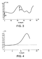
- the angle ⁇ is chosen such that the transmission of the pump beam is in a transmission maximum, for example greater than 70% or 80% or 85%, as indicated by the arrow 10 of the figure 3 .
- This choice also makes it possible to make the system less sensitive to fluctuations introduced during manufacture, to uncertainties as to the angle of incidence or the thicknesses of the layers in the mirror, and to the value of the pumping wavelength.
- the angle ⁇ can also be chosen such that the transmission T of the pump beam is greater than 50%. On the figure 3 this corresponds to an angle of between about 13 ° and 29 °.
- the dielectric mirror by modifying the structure of the dielectric mirror, it can advantageously be transform the transmission curve to obtain a more square profile, ie with a transmission range greater than 50%, more homogeneous, while maintaining the optimum reflectivity for the emission wavelength of the cavity.
- the absorption of the pump beam is optimized by resonating this beam.
- the power of the absorbed pump laser diode in the cavity can be optimized as follows.
- the angle of incidence is chosen to adjust an optical path of the beam coming from the pumping means into the cavity defined by the entrance and exit mirrors of the cavity, so that the cavity also becomes resonant for the length of the cavity. wave of the pump laser diode.
- the wavelength of the pump laser diode ⁇ p can be optimized for maximum absorption of the beams of the pump laser diode in the cavity.
- the optimization can also be performed with the constraint that the reflectivities R e and R s are not affected for the emission wavelength of the laser cavity.
- mirrors than Bragg mirrors, for example metallic mirrors, also make it possible to ensure a high reflectivity for both the wavelength of the pump and the emission.
- Optimization can also be carried out by adapting the value of ⁇ d, for example by modifying the thickness of the absorbent (adaptation of d) or by choosing another material (adaptation of ⁇ ).
- this resonance makes it possible to use small thicknesses of absorbent layers and therefore thin cavities. It is therefore possible to transmit in the fundamental mode (n times more powerful than the n-order mode), which makes it possible to increase the efficiency of the cavity for transmission.
- the efficiency of the emission can be optimized by increasing the absorption.
- the transmission of the pump laser diode is optimized by adjusting the angle of incidence (with a view to good transmission through the input mirror of the emitting cavity, as explained above) and by optimizing the absorption of the pump beam by creating a second cavity resonant at the pumping wavelength.
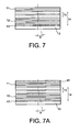
- the figure 7 shows a transmitter having two input mirrors 12, 13, sides diode laser pump, and an output mirror 11 emission side, forming two cavities.
- a first transmission cavity 15 is formed between the input Bragg mirror 12 and the output mirror 11.
- the second cavity 14 is formed between the second input mirror 13 and the output mirror 11.
- the input and output mirrors 11, 13 of the cavity 14 for the pump laser diode preferably respect the absorption maximum condition (2) given above and can be of the Bragg or metallic type.
- This method makes it possible on the one hand to optimize the transmission of the input mirror for the pump beam and, on the other hand, to optimize the efficiency of the latter for pumping the emitting cavity.
- the thickness of the cavity of the pump laser diode which is larger than that of the emitting cavity, makes it easier to obtain a resonance of the pump as a function of the angle and the wavelength ⁇ p of the pump diode.
- the resonance, in the cavity 14, of the pump laser diode can be obtained by adding a thickness of a material of an optical element 43, transparent to the pumping wavelength ⁇ p , between the two mirrors of FIG. input 12 and 13. It is therefore possible to adjust the length of the cavity 14. The angle ⁇ is then chosen so as to optimize the transmission of the input mirror 12 of the emission cavity.
- the efficiency of the device also depends on the divergence of the emission of the pump laser diode. A minimal divergence is therefore preferable.
- An additional lens between the pump laser diode and the transmitter can be used for this purpose in some cases, in particular for diodes emitting by the wafer.
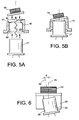
- the Figure 5A shows an embodiment of an assembly according to the invention.
- the transmitter 19 is stuck on the front face of a mounting structure 18.
- the pump laser diode 21 is mounted in a hole or a cavity 50, cylindrical in this example, adapted to receive this diode 21, on the back side of the the mounting structure, and is centered on the axis of the mounting structure.
- the angle ⁇ is defined on the front face 17 of the mounting structure 18 and makes it possible to introduce the optimum angle between the emitter 19 and the emission 20 of the pump laser diode 21 which also comes to rest on the structure 18.
- the Figure 5B shows the different components assembled.
- the figure 6 represents a second embodiment of an assembly, for introducing an optimum angle ⁇ .
- the angle ⁇ is introduced by inclining the hole or cavity 52 for mounting the pump laser diode 26 in the rear face of the mounting structure 25.
- the emission of the pump laser diode is in this case inclined at an angle ⁇ with respect to the axis of the mounting structure.
- the transmitter 23 is bonded to the front face of the mounting structure 25 with a normal to this emitter parallel to the axis 24 of this mounting structure.
- the emitter lobe of the emitter 23 is centered on the axis of the mounting structure.
- This second embodiment has the advantage of facilitating the use of the light emitted by the transmitter.
- the coupling of the light in an optical fiber can in this case be carried out easily by a passive alignment, centered on the axis 24 of the mounting structure.
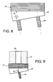
- a pump laser diode of the VCSEL type (abbreviation for Vertical Cavity Surface Emitting Laser), emitting by the rear face.
- the transmitter 27 is mounted on a plate directly on the rear face 28 of a VCSEL 29.
- the angle ⁇ 30 between the normal to the transmitter 27 and the emission direction of the VCSEL 29 is introduced by a polishing of the rear face 28 of VCSEL 29, performed either before or after the manufacture of the VCSEL.
- This support may be, for example, the growth substrate of a pumping VCSEL.
- the figure 9 illustrates an exemplary embodiment of direct coupling of the light in the core 32 of an optical fiber 31.
- the small size of the emission surface thus makes it possible to increase the light coupled in an optical fiber and to reduce the cost of the system , by reducing the components required for assembly and the mounting steps.
- an angle is chosen between the propagation of the pumping beam and the normal of the surface of the emitting microcavity.
- the invention makes it possible to increase the transmitted power, and to stabilize it. It also allows a more reproducible manufacture.
- the emitting devices according to the invention emit preferably in the infrared, for example between 2 microns and 10 microns.
Landscapes
- Physics & Mathematics (AREA)
- Optics & Photonics (AREA)
- Condensed Matter Physics & Semiconductors (AREA)
- General Physics & Mathematics (AREA)
- Electromagnetism (AREA)
- Engineering & Computer Science (AREA)
- Nanotechnology (AREA)
- Chemical & Material Sciences (AREA)
- Biophysics (AREA)
- Crystallography & Structural Chemistry (AREA)
- Life Sciences & Earth Sciences (AREA)
- Semiconductor Lasers (AREA)
- Lasers (AREA)
- Optical Communication System (AREA)
Claims (19)
- Optisch gepumpter Strahlungsemitter, umfassend:- Lichtemissionseinrichtungen (19, 23) mit einem einen ersten Eingangsspiegel (3, 12) und einen Ausgangsspiegel (4, 11) aufweisenden ersten Hohlraumresonator,- optische Pumpeinrichtungen (21, 26) zur Emission eines Pumpstrahls für den ersten Hohlraum, wobei die Normale zur Eingangsfläche des Hohlraums in Bezug auf die Ausbreitungsrichtung des Pumpstrahl (20) um einen Winkel θ geneigt ist,- Einrichtungen (11, 13) zur Bildung eines zweiten Hohlraumresonators für den Pumpstrahl, wobei die genannten Einrichtungen einen mit dem Ausgangsspiegel (11) des ersten Hohlraums den zweiten Hohlraum bildenden zweiten Eingangsspiegel (13) umfassen,dadurch gekennzeichnet, dass er zwischen dem ersten (12) und dem zweiten (13) Eingangsspiegel ein für die Pumpwellenlänge durchlässiges optisches Element (43) umfasst.
- Vorrichtung nach Anspruch 1, wobei der Winkel θ so ist, dass der Pumpstrahl durch den Eingangsspiegel hindurch mit einer Transmission von mehr als 50 % in den ersten Hohlraum transmittiert wird.
- Vorrichtung nach einem der Ansprüche 1 bis 2 mit Spiegeln des Bragg- oder metallischen Typs.
- Vorrichtung nach Anspruch bzw. Ansprüchen 1 bis 3, wobei der Winkel θ so ist, dass der zweite Hohlraum bei der Wellenlänge der optischen Pumpeinrichtungen mischwingt.
- Vorrichtung nach Anspruch bzw. Ansprüchen 1 bis 4, bei der die Reflektivitäten RE und RS des zweiten Eingangsspiegels (13) und des Ausgangsspiegels (11) bei der Wellenlänge der Pumplaserdiode λp folgende Bedingung erfüllen:

- Vorrichtung nach einem der Ansprüche 1 bis 5, wobei die Absorption des Pumpstrahl in dem zweiten Hohlraum höher als 50 % ist.
- Vorrichtung nach einem der Ansprüchen 1 bis 6, wobei die emittierte Strahlung hauptsächlich der Grundmode des zweiten Hohlraums entspricht.
- Vorrichtung nach einem der Ansprüche 1 bis 7, wobei die optischen Pumpeinrichtungen wenigstens einen VCSEL (29) umfassen.
- Vorrichtung nach Anspruch 8, wobei das durch den ersten Hohlraum emittierte Strahlenbündel einen Durchmesser kleiner als 200 µm hat.
- Vorrichtung nach einem der Ansprüche 1 bis 9, wobei die Emissionswellenlänge des ersten Resonators wenigstens partiell zwischen 2 µm und 10 µm entfalten ist.
- Optische Vorrichtung mit einer Vorrichtung nach einem der Ansprüche 1 bis 10 und einer optischen Faser (31), gekoppelt mit dem Ausgang des ersten Hohlraums.
- Vorrichtung nach einem der Ansprüche 1 bis 10 mit einer Montagevorrichtung (18), umfassend:- Einrichtungen (50, 52) um die genannten Pumpeinrichtungen in der Montagevorrichtung zu halten,- Einrichtungen um die Strahlungsemissionsvorrichtungen (19, 23) so zu halten, dass die Normale zur Eingangsfläche dieser Strahlungsemissionseinrichtungen in Bezug auf die Ausbreitungsrichtung eines von den genannten optischen Pumpeinrichtungen stammenden Pumpstrahls um einen Winkel θ geneigt ist,dadurch gekennzeichnet, dass sie zum Halten der Pumpeinrichtungen und der Strahlungsemissionsvorrichtung eine erste und eine zweite Fläche umfasst, wobei diese beiden Flächen zwischen sich einen Winkel θ bilden.
- Vorrichtung nach einem der Ansprüche 1 bis 10 mit einer Montagevorrichtung (18), umfassend:- Einrichtungen (50, 52) um die genannten Pumpeinrichtungen in der Montagevorrichtung zu halten,- Einrichtungen um die Strahlungsemissionsvorrichtungen (19, 23) so zu halten, dass die Normale zur Eingangsfläche dieser Strahlungsemissionseinrichtungen in Bezug auf die Ausbreitungsrichtung eines von den genannten optischen Pumpeinrichtungen stammenden Pumpstrahls um einen Winkel θ geneigt ist,dadurch gekennzeichnet, dass sie das Wachstumssubstrat eines Pump-VCSEL umfasst.
- Vorrichtung nach Anspruch 12, bei der die Montagevorrichtung (18) das Wachstumssubstrat eines Pump-VCSEL umfasst.
- Vorrichtung nach Anspruch 12, wobei die Einrichtungen zum Halten der Pumpeinrichtungen eine in der Zusammenbauvorrichtung vorgesehene Ausnehmung (50, 52) umfassen.
- Vorrichtung nach Anspruch 15, wobei die Ausnehmung rotationssymmetrisch um eine Achse ist, die parallel ist zu einer Längsachse der Zusammenbauvorrichtung.
- Vorrichtung nach Anspruch 16, wobei eine Endfläche (17) der Montagevorrichtung (18) eine Ebene mit einer Normalen definiert, die in Bezug auf diese Längsachse um einen Winkel θ geneigt ist.
- Vorrichtung nach Anspruch 15, wobei die Ausnehmung in Bezug auf eine Längsachse der Montagevorrichtung (18) um einen Winkel θ geneigt ist.
- Vorrichtung nach Anspruch 18, wobei eine Endfläche der Montageeinrichtung eine in Bezug auf diese Längsachse normale Ebene definiert.
Applications Claiming Priority (2)
| Application Number | Priority Date | Filing Date | Title |
|---|---|---|---|
| FR0404803A FR2870051B1 (fr) | 2004-05-04 | 2004-05-04 | Emetteur de rayonnement avec faisceau de pompage incline |
| PCT/FR2005/050292 WO2005109584A2 (fr) | 2004-05-04 | 2005-05-02 | Emetteur de rayonnement avec faisceau de pompage incline |
Publications (2)
| Publication Number | Publication Date |
|---|---|
| EP1745531A2 EP1745531A2 (de) | 2007-01-24 |
| EP1745531B1 true EP1745531B1 (de) | 2009-04-08 |
Family
ID=34946829
Family Applications (1)
| Application Number | Title | Priority Date | Filing Date |
|---|---|---|---|
| EP05759811A Expired - Lifetime EP1745531B1 (de) | 2004-05-04 | 2005-05-02 | Strahlungsemitter mit geneigtem pumpstrahl |
Country Status (7)
| Country | Link |
|---|---|
| US (1) | US20080031300A1 (de) |
| EP (1) | EP1745531B1 (de) |
| JP (1) | JP2007536755A (de) |
| AT (1) | ATE428199T1 (de) |
| DE (1) | DE602005013764D1 (de) |
| FR (1) | FR2870051B1 (de) |
| WO (1) | WO2005109584A2 (de) |
Families Citing this family (2)
| Publication number | Priority date | Publication date | Assignee | Title |
|---|---|---|---|---|
| DE102007061481A1 (de) * | 2007-09-21 | 2009-04-02 | Osram Opto Semiconductors Gmbh | Strahlungsemittierendes Halbleiterbauelement mit vertikaler Emissionsrichtung und Verfahren zur Herstellung eines strahlungsemittierenden Halbleiterbauelements |
| JP2014011442A (ja) * | 2012-07-03 | 2014-01-20 | Alps Electric Co Ltd | 鏡筒付き透光窓および光モジュール |
Family Cites Families (17)
| Publication number | Priority date | Publication date | Assignee | Title |
|---|---|---|---|---|
| US5048047A (en) * | 1990-09-12 | 1991-09-10 | International Business Machines Corporation | Passive absorptive resonator laser system and method |
| JPH05343770A (ja) * | 1992-06-10 | 1993-12-24 | Fuji Photo Film Co Ltd | レーザーダイオードポンピング固体レーザー |
| US5390210A (en) * | 1993-11-22 | 1995-02-14 | Hewlett-Packard Company | Semiconductor laser that generates second harmonic light with attached nonlinear crystal |
| JPH07307509A (ja) * | 1994-05-12 | 1995-11-21 | Ishikawajima Harima Heavy Ind Co Ltd | 固体レーザ |
| US5513204A (en) * | 1995-04-12 | 1996-04-30 | Optical Concepts, Inc. | Long wavelength, vertical cavity surface emitting laser with vertically integrated optical pump |
| DE19517963A1 (de) * | 1995-05-16 | 1996-11-28 | Adlas Gmbh & Co Kg | Longitudinal gepumpter Laser |
| JP3270738B2 (ja) * | 1998-06-11 | 2002-04-02 | 富士写真フイルム株式会社 | 半導体レーザ励起固体レーザ |
| US6252896B1 (en) * | 1999-03-05 | 2001-06-26 | Agilent Technologies, Inc. | Long-Wavelength VCSEL using buried bragg reflectors |
| US6813285B2 (en) * | 1999-06-21 | 2004-11-02 | Litton Systems, Inc. | Q-switched microlaser |
| FR2800364B1 (fr) * | 1999-10-29 | 2002-02-15 | Commissariat Energie Atomique | Microcavite active accordable et procede de fabrication de microcavite active accordable |
| JP2001223429A (ja) * | 2000-02-09 | 2001-08-17 | Fuji Photo Film Co Ltd | 半導体レーザ装置 |
| WO2001078204A1 (en) * | 2000-04-07 | 2001-10-18 | The Government Of The United States Of America, As Represented By The Secretary Of The Navy | Optical pumping injection cavity for optically pumped devices |
| JP3503588B2 (ja) * | 2000-10-30 | 2004-03-08 | 澁谷工業株式会社 | 固体レーザ発振装置 |
| GB2369929A (en) * | 2000-12-08 | 2002-06-12 | Univ Southampton | Semiconductor laser device |
| CA2328637A1 (en) * | 2000-12-15 | 2002-06-15 | Richard D. Clayton | Lateral optical pumping of vertical cavity surface emitting laser |
| FR2833758B1 (fr) * | 2001-12-13 | 2004-12-10 | Commissariat Energie Atomique | Dispositif d'emission de lumiere a micro-cavite et procede de fabrication de ce dispositif |
| FR2833757B1 (fr) * | 2001-12-13 | 2004-11-05 | Commissariat Energie Atomique | Dispositif d'emission de lumiere et procede de fabrication d'un tel dispositif |
-
2004
- 2004-05-04 FR FR0404803A patent/FR2870051B1/fr not_active Expired - Fee Related
-
2005
- 2005-05-02 AT AT05759811T patent/ATE428199T1/de not_active IP Right Cessation
- 2005-05-02 WO PCT/FR2005/050292 patent/WO2005109584A2/fr not_active Ceased
- 2005-05-02 EP EP05759811A patent/EP1745531B1/de not_active Expired - Lifetime
- 2005-05-02 DE DE602005013764T patent/DE602005013764D1/de not_active Expired - Fee Related
- 2005-05-02 US US11/579,508 patent/US20080031300A1/en not_active Abandoned
- 2005-05-02 JP JP2007512300A patent/JP2007536755A/ja active Pending
Also Published As
| Publication number | Publication date |
|---|---|
| EP1745531A2 (de) | 2007-01-24 |
| JP2007536755A (ja) | 2007-12-13 |
| FR2870051A1 (fr) | 2005-11-11 |
| US20080031300A1 (en) | 2008-02-07 |
| WO2005109584A2 (fr) | 2005-11-17 |
| ATE428199T1 (de) | 2009-04-15 |
| FR2870051B1 (fr) | 2009-04-03 |
| WO2005109584A3 (fr) | 2006-06-29 |
| DE602005013764D1 (de) | 2009-05-20 |
Similar Documents
| Publication | Publication Date | Title |
|---|---|---|
| EP0511913B1 (de) | Optoelektronisches Element mit integriertem optischem Wellenleiter und Detektor | |
| EP1454370A2 (de) | Lichtemittierende vorrichtung und herstellungsverfahren | |
| FR3019653A1 (fr) | Dispositif de detection a resonateur acoustique differentiel de type helmholtz | |
| EP0432009A1 (de) | Miniaturlichtquelle und Herstellungsverfahren | |
| FR2741483A1 (fr) | Dispositif optoelectronique a puits quantiques | |
| EP3563140B1 (de) | Vorrichtung zur detektion von gas oder partikeln und verfahren zur herstellung einer solchen vorrichtung | |
| EP2337167A1 (de) | Hybridlaser, mit einem Wellenleiter gekoppelt | |
| EP0006372A1 (de) | Laser mit verteilter Rückkoppelung | |
| EP2460052A1 (de) | Vorrichtung zur steuerung der optischen frequenz und verfahren zur herstellung eines derartigen geräts | |
| FR3070505B1 (fr) | Structure semiconductrice a membrane suspendue en tension comportant une cavite optique | |
| EP0534820B1 (de) | Faseroptische monofrequente Laserquelle mittlerer Leistung | |
| EP1745531B1 (de) | Strahlungsemitter mit geneigtem pumpstrahl | |
| EP1220386B1 (de) | Laserquelle | |
| FR2781613A1 (fr) | Laser en espace libre avec sortie fibre autoalignee | |
| FR3056750A1 (fr) | Detecteur d'une substance fluide | |
| EP0732811A1 (de) | Atomfrequenzstandard | |
| EP2692032B1 (de) | System zur übertragung von optischen signalen | |
| EP4298460A1 (de) | Optoelektronischer emitter mit phasengesteuerter gruppenantenne mit aufgeweiteter laserquelle | |
| EP1454394B1 (de) | Licht emittierende vorrichtung mit einem mikroresonator und herstellungsverfahren | |
| EP1433232B1 (de) | Wellenleiterlaserquelle | |
| EP4627684A1 (de) | Oberflächenemittierende vorrichtung, optisches system und zugehöriges verfahren | |
| EP4557537A1 (de) | Integrierte hochleistungslaseremissionsvorrichtung | |
| EP1880451A1 (de) | Optische pumpvorrichtung | |
| FR2739732A1 (fr) | Dispositif d'amplification optique | |
| EP3936763A1 (de) | Lumineszenzkonzentrator |
Legal Events
| Date | Code | Title | Description |
|---|---|---|---|
| PUAI | Public reference made under article 153(3) epc to a published international application that has entered the european phase |
Free format text: ORIGINAL CODE: 0009012 |
|
| 17P | Request for examination filed |
Effective date: 20061108 |
|
| AK | Designated contracting states |
Kind code of ref document: A2 Designated state(s): AT BE BG CH CY CZ DE DK EE ES FI FR GB GR HU IE IS IT LI LT LU MC NL PL PT RO SE SI SK TR |
|
| AX | Request for extension of the european patent |
Extension state: AL BA HR LV MK YU |
|
| DAX | Request for extension of the european patent (deleted) | ||
| GRAP | Despatch of communication of intention to grant a patent |
Free format text: ORIGINAL CODE: EPIDOSNIGR1 |
|
| GRAP | Despatch of communication of intention to grant a patent |
Free format text: ORIGINAL CODE: EPIDOSNIGR1 |
|
| GRAS | Grant fee paid |
Free format text: ORIGINAL CODE: EPIDOSNIGR3 |
|
| GRAA | (expected) grant |
Free format text: ORIGINAL CODE: 0009210 |
|
| AK | Designated contracting states |
Kind code of ref document: B1 Designated state(s): AT BE BG CH CY CZ DE DK EE ES FI FR GB GR HU IE IS IT LI LT LU MC NL PL PT RO SE SI SK TR |
|
| REG | Reference to a national code |
Ref country code: GB Ref legal event code: FG4D Free format text: NOT ENGLISH |
|
| REG | Reference to a national code |
Ref country code: CH Ref legal event code: EP |
|
| REG | Reference to a national code |
Ref country code: IE Ref legal event code: FG4D |
|
| REF | Corresponds to: |
Ref document number: 602005013764 Country of ref document: DE Date of ref document: 20090520 Kind code of ref document: P |
|
| PG25 | Lapsed in a contracting state [announced via postgrant information from national office to epo] |
Ref country code: SI Free format text: LAPSE BECAUSE OF FAILURE TO SUBMIT A TRANSLATION OF THE DESCRIPTION OR TO PAY THE FEE WITHIN THE PRESCRIBED TIME-LIMIT Effective date: 20090408 |
|
| REG | Reference to a national code |
Ref country code: SE Ref legal event code: TRGR |
|
| PGFP | Annual fee paid to national office [announced via postgrant information from national office to epo] |
Ref country code: DE Payment date: 20090525 Year of fee payment: 5 Ref country code: FR Payment date: 20090513 Year of fee payment: 5 Ref country code: IT Payment date: 20090526 Year of fee payment: 5 |
|
| NLV1 | Nl: lapsed or annulled due to failure to fulfill the requirements of art. 29p and 29m of the patents act | ||
| REG | Reference to a national code |
Ref country code: IE Ref legal event code: FD4D |
|
| PG25 | Lapsed in a contracting state [announced via postgrant information from national office to epo] |
Ref country code: PT Free format text: LAPSE BECAUSE OF FAILURE TO SUBMIT A TRANSLATION OF THE DESCRIPTION OR TO PAY THE FEE WITHIN THE PRESCRIBED TIME-LIMIT Effective date: 20090908 Ref country code: LT Free format text: LAPSE BECAUSE OF FAILURE TO SUBMIT A TRANSLATION OF THE DESCRIPTION OR TO PAY THE FEE WITHIN THE PRESCRIBED TIME-LIMIT Effective date: 20090408 Ref country code: FI Free format text: LAPSE BECAUSE OF FAILURE TO SUBMIT A TRANSLATION OF THE DESCRIPTION OR TO PAY THE FEE WITHIN THE PRESCRIBED TIME-LIMIT Effective date: 20090408 Ref country code: ES Free format text: LAPSE BECAUSE OF FAILURE TO SUBMIT A TRANSLATION OF THE DESCRIPTION OR TO PAY THE FEE WITHIN THE PRESCRIBED TIME-LIMIT Effective date: 20090719 Ref country code: AT Free format text: LAPSE BECAUSE OF FAILURE TO SUBMIT A TRANSLATION OF THE DESCRIPTION OR TO PAY THE FEE WITHIN THE PRESCRIBED TIME-LIMIT Effective date: 20090408 |
|
| BERE | Be: lapsed |
Owner name: COMMISSARIAT A L'ENERGIE ATOMIQUE Effective date: 20090531 |
|
| PG25 | Lapsed in a contracting state [announced via postgrant information from national office to epo] |
Ref country code: NL Free format text: LAPSE BECAUSE OF FAILURE TO SUBMIT A TRANSLATION OF THE DESCRIPTION OR TO PAY THE FEE WITHIN THE PRESCRIBED TIME-LIMIT Effective date: 20090408 Ref country code: PL Free format text: LAPSE BECAUSE OF FAILURE TO SUBMIT A TRANSLATION OF THE DESCRIPTION OR TO PAY THE FEE WITHIN THE PRESCRIBED TIME-LIMIT Effective date: 20090408 Ref country code: IS Free format text: LAPSE BECAUSE OF FAILURE TO SUBMIT A TRANSLATION OF THE DESCRIPTION OR TO PAY THE FEE WITHIN THE PRESCRIBED TIME-LIMIT Effective date: 20090808 |
|
| PGFP | Annual fee paid to national office [announced via postgrant information from national office to epo] |
Ref country code: GB Payment date: 20090522 Year of fee payment: 5 |
|
| PG25 | Lapsed in a contracting state [announced via postgrant information from national office to epo] |
Ref country code: MC Free format text: LAPSE BECAUSE OF NON-PAYMENT OF DUE FEES Effective date: 20090531 |
|
| REG | Reference to a national code |
Ref country code: CH Ref legal event code: PL |
|
| PG25 | Lapsed in a contracting state [announced via postgrant information from national office to epo] |
Ref country code: RO Free format text: LAPSE BECAUSE OF FAILURE TO SUBMIT A TRANSLATION OF THE DESCRIPTION OR TO PAY THE FEE WITHIN THE PRESCRIBED TIME-LIMIT Effective date: 20090408 Ref country code: IE Free format text: LAPSE BECAUSE OF FAILURE TO SUBMIT A TRANSLATION OF THE DESCRIPTION OR TO PAY THE FEE WITHIN THE PRESCRIBED TIME-LIMIT Effective date: 20090408 Ref country code: CH Free format text: LAPSE BECAUSE OF NON-PAYMENT OF DUE FEES Effective date: 20090531 Ref country code: CZ Free format text: LAPSE BECAUSE OF FAILURE TO SUBMIT A TRANSLATION OF THE DESCRIPTION OR TO PAY THE FEE WITHIN THE PRESCRIBED TIME-LIMIT Effective date: 20090408 Ref country code: LI Free format text: LAPSE BECAUSE OF NON-PAYMENT OF DUE FEES Effective date: 20090531 Ref country code: DK Free format text: LAPSE BECAUSE OF FAILURE TO SUBMIT A TRANSLATION OF THE DESCRIPTION OR TO PAY THE FEE WITHIN THE PRESCRIBED TIME-LIMIT Effective date: 20090408 Ref country code: EE Free format text: LAPSE BECAUSE OF FAILURE TO SUBMIT A TRANSLATION OF THE DESCRIPTION OR TO PAY THE FEE WITHIN THE PRESCRIBED TIME-LIMIT Effective date: 20090408 |
|
| PLBE | No opposition filed within time limit |
Free format text: ORIGINAL CODE: 0009261 |
|
| STAA | Information on the status of an ep patent application or granted ep patent |
Free format text: STATUS: NO OPPOSITION FILED WITHIN TIME LIMIT |
|
| PG25 | Lapsed in a contracting state [announced via postgrant information from national office to epo] |
Ref country code: SK Free format text: LAPSE BECAUSE OF FAILURE TO SUBMIT A TRANSLATION OF THE DESCRIPTION OR TO PAY THE FEE WITHIN THE PRESCRIBED TIME-LIMIT Effective date: 20090408 |
|
| 26N | No opposition filed |
Effective date: 20100111 |
|
| PG25 | Lapsed in a contracting state [announced via postgrant information from national office to epo] |
Ref country code: BG Free format text: LAPSE BECAUSE OF FAILURE TO SUBMIT A TRANSLATION OF THE DESCRIPTION OR TO PAY THE FEE WITHIN THE PRESCRIBED TIME-LIMIT Effective date: 20090708 |
|
| PG25 | Lapsed in a contracting state [announced via postgrant information from national office to epo] |
Ref country code: BE Free format text: LAPSE BECAUSE OF NON-PAYMENT OF DUE FEES Effective date: 20090531 |
|
| PG25 | Lapsed in a contracting state [announced via postgrant information from national office to epo] |
Ref country code: GR Free format text: LAPSE BECAUSE OF FAILURE TO SUBMIT A TRANSLATION OF THE DESCRIPTION OR TO PAY THE FEE WITHIN THE PRESCRIBED TIME-LIMIT Effective date: 20090709 |
|
| GBPC | Gb: european patent ceased through non-payment of renewal fee |
Effective date: 20100502 |
|
| EUG | Se: european patent has lapsed | ||
| REG | Reference to a national code |
Ref country code: FR Ref legal event code: ST Effective date: 20110131 |
|
| PG25 | Lapsed in a contracting state [announced via postgrant information from national office to epo] |
Ref country code: IT Free format text: LAPSE BECAUSE OF NON-PAYMENT OF DUE FEES Effective date: 20100502 Ref country code: SE Free format text: LAPSE BECAUSE OF NON-PAYMENT OF DUE FEES Effective date: 20100503 |
|
| PG25 | Lapsed in a contracting state [announced via postgrant information from national office to epo] |
Ref country code: DE Free format text: LAPSE BECAUSE OF NON-PAYMENT OF DUE FEES Effective date: 20101201 Ref country code: LU Free format text: LAPSE BECAUSE OF NON-PAYMENT OF DUE FEES Effective date: 20090502 |
|
| PG25 | Lapsed in a contracting state [announced via postgrant information from national office to epo] |
Ref country code: FR Free format text: LAPSE BECAUSE OF NON-PAYMENT OF DUE FEES Effective date: 20100531 |
|
| PG25 | Lapsed in a contracting state [announced via postgrant information from national office to epo] |
Ref country code: HU Free format text: LAPSE BECAUSE OF FAILURE TO SUBMIT A TRANSLATION OF THE DESCRIPTION OR TO PAY THE FEE WITHIN THE PRESCRIBED TIME-LIMIT Effective date: 20091009 |
|
| PG25 | Lapsed in a contracting state [announced via postgrant information from national office to epo] |
Ref country code: GB Free format text: LAPSE BECAUSE OF NON-PAYMENT OF DUE FEES Effective date: 20100502 |
|
| PG25 | Lapsed in a contracting state [announced via postgrant information from national office to epo] |
Ref country code: TR Free format text: LAPSE BECAUSE OF FAILURE TO SUBMIT A TRANSLATION OF THE DESCRIPTION OR TO PAY THE FEE WITHIN THE PRESCRIBED TIME-LIMIT Effective date: 20090408 |
|
| PG25 | Lapsed in a contracting state [announced via postgrant information from national office to epo] |
Ref country code: CY Free format text: LAPSE BECAUSE OF FAILURE TO SUBMIT A TRANSLATION OF THE DESCRIPTION OR TO PAY THE FEE WITHIN THE PRESCRIBED TIME-LIMIT Effective date: 20090408 |
|
| PGFP | Annual fee paid to national office [announced via postgrant information from national office to epo] |
Ref country code: SE Payment date: 20090514 Year of fee payment: 5 |