EP1745531B1 - Inclined pump beam radiation emitter - Google Patents
Inclined pump beam radiation emitter Download PDFInfo
- Publication number
- EP1745531B1 EP1745531B1 EP05759811A EP05759811A EP1745531B1 EP 1745531 B1 EP1745531 B1 EP 1745531B1 EP 05759811 A EP05759811 A EP 05759811A EP 05759811 A EP05759811 A EP 05759811A EP 1745531 B1 EP1745531 B1 EP 1745531B1
- Authority
- EP
- European Patent Office
- Prior art keywords
- pumping
- cavity
- angle
- optical
- mirror
- Prior art date
- Legal status (The legal status is an assumption and is not a legal conclusion. Google has not performed a legal analysis and makes no representation as to the accuracy of the status listed.)
- Expired - Lifetime
Links
- 230000005855 radiation Effects 0.000 title claims abstract description 20
- 238000005086 pumping Methods 0.000 claims abstract description 65
- 230000003287 optical effect Effects 0.000 claims abstract description 29
- 238000010521 absorption reaction Methods 0.000 claims description 29
- 230000005540 biological transmission Effects 0.000 claims description 27
- 239000013307 optical fiber Substances 0.000 claims description 8
- 238000002310 reflectometry Methods 0.000 claims description 7
- 239000000758 substrate Substances 0.000 claims description 5
- 235000021183 entrée Nutrition 0.000 description 7
- 238000004519 manufacturing process Methods 0.000 description 7
- 230000004888 barrier function Effects 0.000 description 5
- 230000008901 benefit Effects 0.000 description 5
- 230000008878 coupling Effects 0.000 description 5
- 238000010168 coupling process Methods 0.000 description 5
- 238000005859 coupling reaction Methods 0.000 description 5
- 230000002745 absorbent Effects 0.000 description 4
- 239000002250 absorbent Substances 0.000 description 4
- 239000000969 carrier Substances 0.000 description 4
- 239000007789 gas Substances 0.000 description 4
- 239000000463 material Substances 0.000 description 4
- 238000005457 optimization Methods 0.000 description 4
- 238000009412 basement excavation Methods 0.000 description 3
- 238000001514 detection method Methods 0.000 description 3
- 230000009467 reduction Effects 0.000 description 3
- 235000014698 Brassica juncea var multisecta Nutrition 0.000 description 2
- 241000251184 Rajiformes Species 0.000 description 2
- 230000006978 adaptation Effects 0.000 description 2
- 238000009792 diffusion process Methods 0.000 description 2
- 230000000694 effects Effects 0.000 description 2
- 239000000835 fiber Substances 0.000 description 2
- 239000004065 semiconductor Substances 0.000 description 2
- 241001644893 Entandrophragma utile Species 0.000 description 1
- 229910000673 Indium arsenide Inorganic materials 0.000 description 1
- 229910000661 Mercury cadmium telluride Inorganic materials 0.000 description 1
- 230000000712 assembly Effects 0.000 description 1
- 238000000429 assembly Methods 0.000 description 1
- 230000003416 augmentation Effects 0.000 description 1
- 230000008859 change Effects 0.000 description 1
- 230000001427 coherent effect Effects 0.000 description 1
- 229940082150 encore Drugs 0.000 description 1
- RPQDHPTXJYYUPQ-UHFFFAOYSA-N indium arsenide Chemical compound [In]#[As] RPQDHPTXJYYUPQ-UHFFFAOYSA-N 0.000 description 1
- 238000000034 method Methods 0.000 description 1
- 230000010363 phase shift Effects 0.000 description 1
- 239000004033 plastic Substances 0.000 description 1
- 229920003023 plastic Polymers 0.000 description 1
- 238000005498 polishing Methods 0.000 description 1
- 230000006798 recombination Effects 0.000 description 1
- 238000005215 recombination Methods 0.000 description 1
- 230000003595 spectral effect Effects 0.000 description 1
- 230000001360 synchronised effect Effects 0.000 description 1
Images

Classifications
-
- H—ELECTRICITY
- H01—ELECTRIC ELEMENTS
- H01S—DEVICES USING THE PROCESS OF LIGHT AMPLIFICATION BY STIMULATED EMISSION OF RADIATION [LASER] TO AMPLIFY OR GENERATE LIGHT; DEVICES USING STIMULATED EMISSION OF ELECTROMAGNETIC RADIATION IN WAVE RANGES OTHER THAN OPTICAL
- H01S5/00—Semiconductor lasers
- H01S5/04—Processes or apparatus for excitation, e.g. pumping, e.g. by electron beams
- H01S5/041—Optical pumping
-
- B—PERFORMING OPERATIONS; TRANSPORTING
- B82—NANOTECHNOLOGY
- B82Y—SPECIFIC USES OR APPLICATIONS OF NANOSTRUCTURES; MEASUREMENT OR ANALYSIS OF NANOSTRUCTURES; MANUFACTURE OR TREATMENT OF NANOSTRUCTURES
- B82Y20/00—Nanooptics, e.g. quantum optics or photonic crystals
-
- H—ELECTRICITY
- H01—ELECTRIC ELEMENTS
- H01S—DEVICES USING THE PROCESS OF LIGHT AMPLIFICATION BY STIMULATED EMISSION OF RADIATION [LASER] TO AMPLIFY OR GENERATE LIGHT; DEVICES USING STIMULATED EMISSION OF ELECTROMAGNETIC RADIATION IN WAVE RANGES OTHER THAN OPTICAL
- H01S5/00—Semiconductor lasers
- H01S5/02—Structural details or components not essential to laser action
- H01S5/022—Mountings; Housings
- H01S5/0225—Out-coupling of light
- H01S5/02257—Out-coupling of light using windows, e.g. specially adapted for back-reflecting light to a detector inside the housing
-
- H—ELECTRICITY
- H01—ELECTRIC ELEMENTS
- H01S—DEVICES USING THE PROCESS OF LIGHT AMPLIFICATION BY STIMULATED EMISSION OF RADIATION [LASER] TO AMPLIFY OR GENERATE LIGHT; DEVICES USING STIMULATED EMISSION OF ELECTROMAGNETIC RADIATION IN WAVE RANGES OTHER THAN OPTICAL
- H01S5/00—Semiconductor lasers
- H01S5/02—Structural details or components not essential to laser action
- H01S5/026—Monolithically integrated components, e.g. waveguides, monitoring photo-detectors, drivers
-
- H—ELECTRICITY
- H01—ELECTRIC ELEMENTS
- H01S—DEVICES USING THE PROCESS OF LIGHT AMPLIFICATION BY STIMULATED EMISSION OF RADIATION [LASER] TO AMPLIFY OR GENERATE LIGHT; DEVICES USING STIMULATED EMISSION OF ELECTROMAGNETIC RADIATION IN WAVE RANGES OTHER THAN OPTICAL
- H01S5/00—Semiconductor lasers
- H01S5/10—Construction or shape of the optical resonator, e.g. extended or external cavity, coupled cavities, bent-guide, varying width, thickness or composition of the active region
- H01S5/18—Surface-emitting [SE] lasers, e.g. having both horizontal and vertical cavities
- H01S5/183—Surface-emitting [SE] lasers, e.g. having both horizontal and vertical cavities having only vertical cavities, e.g. vertical cavity surface-emitting lasers [VCSEL]
- H01S5/18361—Structure of the reflectors, e.g. hybrid mirrors
- H01S5/18369—Structure of the reflectors, e.g. hybrid mirrors based on dielectric materials
-
- H—ELECTRICITY
- H01—ELECTRIC ELEMENTS
- H01S—DEVICES USING THE PROCESS OF LIGHT AMPLIFICATION BY STIMULATED EMISSION OF RADIATION [LASER] TO AMPLIFY OR GENERATE LIGHT; DEVICES USING STIMULATED EMISSION OF ELECTROMAGNETIC RADIATION IN WAVE RANGES OTHER THAN OPTICAL
- H01S5/00—Semiconductor lasers
- H01S5/02—Structural details or components not essential to laser action
- H01S5/0206—Substrates, e.g. growth, shape, material, removal or bonding
- H01S5/0207—Substrates having a special shape
-
- H—ELECTRICITY
- H01—ELECTRIC ELEMENTS
- H01S—DEVICES USING THE PROCESS OF LIGHT AMPLIFICATION BY STIMULATED EMISSION OF RADIATION [LASER] TO AMPLIFY OR GENERATE LIGHT; DEVICES USING STIMULATED EMISSION OF ELECTROMAGNETIC RADIATION IN WAVE RANGES OTHER THAN OPTICAL
- H01S5/00—Semiconductor lasers
- H01S5/02—Structural details or components not essential to laser action
- H01S5/022—Mountings; Housings
- H01S5/0225—Out-coupling of light
- H01S5/02251—Out-coupling of light using optical fibres
-
- H—ELECTRICITY
- H01—ELECTRIC ELEMENTS
- H01S—DEVICES USING THE PROCESS OF LIGHT AMPLIFICATION BY STIMULATED EMISSION OF RADIATION [LASER] TO AMPLIFY OR GENERATE LIGHT; DEVICES USING STIMULATED EMISSION OF ELECTROMAGNETIC RADIATION IN WAVE RANGES OTHER THAN OPTICAL
- H01S5/00—Semiconductor lasers
- H01S5/30—Structure or shape of the active region; Materials used for the active region
- H01S5/34—Structure or shape of the active region; Materials used for the active region comprising quantum well or superlattice structures, e.g. single quantum well [SQW] lasers, multiple quantum well [MQW] lasers or graded index separate confinement heterostructure [GRINSCH] lasers
- H01S5/347—Structure or shape of the active region; Materials used for the active region comprising quantum well or superlattice structures, e.g. single quantum well [SQW] lasers, multiple quantum well [MQW] lasers or graded index separate confinement heterostructure [GRINSCH] lasers in AIIBVI compounds, e.g. ZnCdSe- laser
-
- H—ELECTRICITY
- H01—ELECTRIC ELEMENTS
- H01S—DEVICES USING THE PROCESS OF LIGHT AMPLIFICATION BY STIMULATED EMISSION OF RADIATION [LASER] TO AMPLIFY OR GENERATE LIGHT; DEVICES USING STIMULATED EMISSION OF ELECTROMAGNETIC RADIATION IN WAVE RANGES OTHER THAN OPTICAL
- H01S5/00—Semiconductor lasers
- H01S5/40—Arrangement of two or more semiconductor lasers, not provided for in groups H01S5/02 - H01S5/30
- H01S5/4025—Array arrangements, e.g. constituted by discrete laser diodes or laser bar
- H01S5/4031—Edge-emitting structures
- H01S5/4056—Edge-emitting structures emitting light in more than one direction
-
- H—ELECTRICITY
- H01—ELECTRIC ELEMENTS
- H01S—DEVICES USING THE PROCESS OF LIGHT AMPLIFICATION BY STIMULATED EMISSION OF RADIATION [LASER] TO AMPLIFY OR GENERATE LIGHT; DEVICES USING STIMULATED EMISSION OF ELECTROMAGNETIC RADIATION IN WAVE RANGES OTHER THAN OPTICAL
- H01S5/00—Semiconductor lasers
- H01S5/40—Arrangement of two or more semiconductor lasers, not provided for in groups H01S5/02 - H01S5/30
- H01S5/42—Arrays of surface emitting lasers
- H01S5/423—Arrays of surface emitting lasers having a vertical cavity
Definitions
- the invention relates to the field of light emitters.
- infrared light emitters that can be used, for example, for the detection of gas and the sorting of plastics.
- Such a transmitter can also be used to detect polluting gases in the exhaust pipes of cars.
- Filtered filaments have low intensities but can be used in combination with synchronous detection.
- microcavity used in such a transmitter is schematically illustrated on the figure 1 .
- An emitter layer 1 is sandwiched between two barrier layers 2 and two Bragg mirrors 3 and 4.
- the cavity rests on a substrate 5, for mechanical reasons.
- the barrier layers 2 serve to create photo-carriers by the absorption of the photons of a pump laser diode.
- the IR emission is generated by the recombination of the photo-carriers in the emitter layer 1.
- the emission of the microcavity is determined in particular by the absorption of the pump laser diode.
- the layer thicknesses in the cavity are further adapted so that the cavity is resonant at the wavelength of the emission.
- the thicknesses of the barriers 2 are such that approximately 60% of the pump light is absorbed in the cavity, thus limiting the emitted power of the emitter.
- the figure 2 illustrates an example of a standard transmitter system.
- a microcavity 6 is mounted on a mounting structure 7 which makes it possible to assemble the microcavity with pumping means 8, for example a laser diode.
- Part of the radiation of the pump laser diode is reflected by the cavity 6 entrance mirror.
- Part of the optical power of the pump laser diode can therefore be reflected in the same diode, thus creating power instabilities.
- the reflected light represents a loss of intensity of the pump beams and thus causes a loss of the emission of the transmitter.
- This reflected light can also generate instabilities of the pump diode 8.
- This problem can be solved by choosing a wavelength of the pumping diode, which will be less reflected, with the disadvantage of an additional cost generated by the development. a specific pumping diode for each wavelength.
- the invention proposes a system that makes it possible to optimize the emission of a light emitter by optimizing or improving the transmission of a pumping beam through an input mirror of the transmitter and / or optimizing or improving the absorption, in a resonant cavity of the transmitter, of a pumping beam of a pump diode used to optically excite carriers in the transmitter device.
- the resonant cavity is inclined by an angle ⁇ such that the pump beam is transmitted in the first cavity through the input face with a transmission greater than 50%.
- the mirrors can be of Bragg type or metallic.
- the absorption of the pump beam in the second cavity may be greater than 50%.
- the radiation is mainly emitted according to the fundamental mode of the second resonant cavity.
- the optical pumping means may advantageously comprise at least one VCSEL.
- the radiation beam emitted by the first resonant cavity may have a diameter of less than 200 ⁇ m.
- the emission wavelength of the first cavity is for example at least partially between 2 microns and 10 microns.
- the invention also relates to an optical device comprising a device as described above and an optical fiber coupled with the output of the first resonant cavity.
- the invention therefore proposes various means for increasing the power emitted for a given power of a pump diode, by optimizing the transmission and / or the absorption of the beam of the pump diode.
- the invention also proposes various means for assembling the pump diode and the transmitter.
- a support device comprising means for maintaining a non-zero angle ⁇ , for example between 10 ° and 30 °, between a direction of propagation of a pumping beam of a pumping means of a resonant cavity and a normal to a face or an entrance mirror of this cavity.
- This support may be, for example, the growth substrate of a pumping VCSEL.
- the means for maintaining the pumping means may comprise an excavation made in an assembly device.
- the excavation may be symmetrical of revolution about an axis parallel to a longitudinal axis of the assembly device.
- an end surface of this assembly device can define a plane having a normal inclined at an angle ⁇ with respect to this longitudinal axis.
- the excavation can be inclined at an angle ⁇ relative to a longitudinal axis of the assembly device.
- an end surface of this assembly device defines a normal plane with respect to this longitudinal axis.
- the angle ⁇ makes it possible to avoid the reflection of the light of the pump beam in the cavity, thus eliminating the instabilities in the pumping means.
- the angle ⁇ is preferably chosen to optimize the absorption of the pump when the wavelength is fixed.
- the invention applies to a light emitting device, coherent or not, such as by example shown on the figure 1 .
- a light emitting device coherent or not, such as by example shown on the figure 1 .
- Such a device is pumped optically using the pumping means.
- the material of the emitting layer can therefore be in Hg 1-x Cd x Te.
- Other examples of usable materials are semiconductors III-IV (InAs 1-x Sb x , or Ga 1-x In x Sb or Ga 1-x In x As 1-y Sb y ) or semiconductors of type IV-VI (Pb 1-x Sn x Te or Pb 1-x Sn x Se).
- a first embodiment of the invention relates to optimizing the absorption of the pump beam by optimizing or maximizing the transmission of the pump beam through the entrance mirror of a cavity such as that illustrated. in figure 1 .
- the transmission of a Bragg mirror depends on the stacking of the layers of this mirror, the thicknesses and indices of these layers, the wavelength of the radiation but also the angle of incidence of the radiation.
- a change in the angle of incidence increases the optical path between the interfaces of each layer of the Bragg mirror and allows the transmission to be changed through this mirror.
- a mirror which is optimized for maximum reflection of the transmitter at an emission wavelength ⁇ E can thus be made as transparent as possible for the wavelength of the pump laser diode.
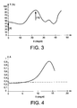
- the angle ⁇ is chosen such that the transmission of the pump beam is in a transmission maximum, for example greater than 70% or 80% or 85%, as indicated by the arrow 10 of the figure 3 .
- This choice also makes it possible to make the system less sensitive to fluctuations introduced during manufacture, to uncertainties as to the angle of incidence or the thicknesses of the layers in the mirror, and to the value of the pumping wavelength.
- the angle ⁇ can also be chosen such that the transmission T of the pump beam is greater than 50%. On the figure 3 this corresponds to an angle of between about 13 ° and 29 °.
- the dielectric mirror by modifying the structure of the dielectric mirror, it can advantageously be transform the transmission curve to obtain a more square profile, ie with a transmission range greater than 50%, more homogeneous, while maintaining the optimum reflectivity for the emission wavelength of the cavity.
- the absorption of the pump beam is optimized by resonating this beam.
- the power of the absorbed pump laser diode in the cavity can be optimized as follows.
- the angle of incidence is chosen to adjust an optical path of the beam coming from the pumping means into the cavity defined by the entrance and exit mirrors of the cavity, so that the cavity also becomes resonant for the length of the cavity. wave of the pump laser diode.
- the wavelength of the pump laser diode ⁇ p can be optimized for maximum absorption of the beams of the pump laser diode in the cavity.
- the optimization can also be performed with the constraint that the reflectivities R e and R s are not affected for the emission wavelength of the laser cavity.
- mirrors than Bragg mirrors, for example metallic mirrors, also make it possible to ensure a high reflectivity for both the wavelength of the pump and the emission.
- Optimization can also be carried out by adapting the value of ⁇ d, for example by modifying the thickness of the absorbent (adaptation of d) or by choosing another material (adaptation of ⁇ ).
- this resonance makes it possible to use small thicknesses of absorbent layers and therefore thin cavities. It is therefore possible to transmit in the fundamental mode (n times more powerful than the n-order mode), which makes it possible to increase the efficiency of the cavity for transmission.
- the efficiency of the emission can be optimized by increasing the absorption.
- the transmission of the pump laser diode is optimized by adjusting the angle of incidence (with a view to good transmission through the input mirror of the emitting cavity, as explained above) and by optimizing the absorption of the pump beam by creating a second cavity resonant at the pumping wavelength.
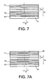
- the figure 7 shows a transmitter having two input mirrors 12, 13, sides diode laser pump, and an output mirror 11 emission side, forming two cavities.
- a first transmission cavity 15 is formed between the input Bragg mirror 12 and the output mirror 11.
- the second cavity 14 is formed between the second input mirror 13 and the output mirror 11.
- the input and output mirrors 11, 13 of the cavity 14 for the pump laser diode preferably respect the absorption maximum condition (2) given above and can be of the Bragg or metallic type.
- This method makes it possible on the one hand to optimize the transmission of the input mirror for the pump beam and, on the other hand, to optimize the efficiency of the latter for pumping the emitting cavity.
- the thickness of the cavity of the pump laser diode which is larger than that of the emitting cavity, makes it easier to obtain a resonance of the pump as a function of the angle and the wavelength ⁇ p of the pump diode.
- the resonance, in the cavity 14, of the pump laser diode can be obtained by adding a thickness of a material of an optical element 43, transparent to the pumping wavelength ⁇ p , between the two mirrors of FIG. input 12 and 13. It is therefore possible to adjust the length of the cavity 14. The angle ⁇ is then chosen so as to optimize the transmission of the input mirror 12 of the emission cavity.
- the efficiency of the device also depends on the divergence of the emission of the pump laser diode. A minimal divergence is therefore preferable.
- An additional lens between the pump laser diode and the transmitter can be used for this purpose in some cases, in particular for diodes emitting by the wafer.
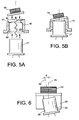
- the Figure 5A shows an embodiment of an assembly according to the invention.
- the transmitter 19 is stuck on the front face of a mounting structure 18.
- the pump laser diode 21 is mounted in a hole or a cavity 50, cylindrical in this example, adapted to receive this diode 21, on the back side of the the mounting structure, and is centered on the axis of the mounting structure.
- the angle ⁇ is defined on the front face 17 of the mounting structure 18 and makes it possible to introduce the optimum angle between the emitter 19 and the emission 20 of the pump laser diode 21 which also comes to rest on the structure 18.
- the Figure 5B shows the different components assembled.
- the figure 6 represents a second embodiment of an assembly, for introducing an optimum angle ⁇ .
- the angle ⁇ is introduced by inclining the hole or cavity 52 for mounting the pump laser diode 26 in the rear face of the mounting structure 25.
- the emission of the pump laser diode is in this case inclined at an angle ⁇ with respect to the axis of the mounting structure.
- the transmitter 23 is bonded to the front face of the mounting structure 25 with a normal to this emitter parallel to the axis 24 of this mounting structure.
- the emitter lobe of the emitter 23 is centered on the axis of the mounting structure.
- This second embodiment has the advantage of facilitating the use of the light emitted by the transmitter.
- the coupling of the light in an optical fiber can in this case be carried out easily by a passive alignment, centered on the axis 24 of the mounting structure.
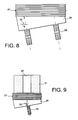
- a pump laser diode of the VCSEL type (abbreviation for Vertical Cavity Surface Emitting Laser), emitting by the rear face.
- the transmitter 27 is mounted on a plate directly on the rear face 28 of a VCSEL 29.
- the angle ⁇ 30 between the normal to the transmitter 27 and the emission direction of the VCSEL 29 is introduced by a polishing of the rear face 28 of VCSEL 29, performed either before or after the manufacture of the VCSEL.
- This support may be, for example, the growth substrate of a pumping VCSEL.
- the figure 9 illustrates an exemplary embodiment of direct coupling of the light in the core 32 of an optical fiber 31.
- the small size of the emission surface thus makes it possible to increase the light coupled in an optical fiber and to reduce the cost of the system , by reducing the components required for assembly and the mounting steps.
- an angle is chosen between the propagation of the pumping beam and the normal of the surface of the emitting microcavity.
- the invention makes it possible to increase the transmitted power, and to stabilize it. It also allows a more reproducible manufacture.
- the emitting devices according to the invention emit preferably in the infrared, for example between 2 microns and 10 microns.
Landscapes
- Physics & Mathematics (AREA)
- Optics & Photonics (AREA)
- Condensed Matter Physics & Semiconductors (AREA)
- General Physics & Mathematics (AREA)
- Electromagnetism (AREA)
- Engineering & Computer Science (AREA)
- Nanotechnology (AREA)
- Chemical & Material Sciences (AREA)
- Biophysics (AREA)
- Crystallography & Structural Chemistry (AREA)
- Life Sciences & Earth Sciences (AREA)
- Semiconductor Lasers (AREA)
- Lasers (AREA)
- Optical Communication System (AREA)
Abstract
Description
L'invention concerne le domaine des émetteurs de lumière.The invention relates to the field of light emitters.
Elle concerne notamment la réalisation d'émetteurs de lumière Infra Rouge pouvant être utilisés, par exemple, pour la détection de gaz et le tri des plastiques.It relates in particular to the production of infrared light emitters that can be used, for example, for the detection of gas and the sorting of plastics.
Un tel émetteur peut être aussi utilisé pour détecter des gaz polluants dans les pots d'échappement des voitures.Such a transmitter can also be used to detect polluting gases in the exhaust pipes of cars.
La détection du gaz par moyen optique dans la gamme de longueur d'onde de 3-5 µm présente de nombreux avantages :
- les raies d'absorption sont intenses,
- les raies d'absorption sont, pour les gaz les plus importants, bien séparées en longueurs d'onde.
- the absorption lines are intense,
- the absorption lines are, for the largest gases, well separated in wavelengths.
La difficulté d'utiliser cette gamme de longueurs d'onde est qu'il y a peu de sources disponibles, suffisamment intenses et directionnelles.The difficulty in using this range of wavelengths is that there are few sources available, sufficiently intense and directional.
Les lasers basés sur des effets de cascade quantique sont trop coûteux et très complexes à réaliser.Lasers based on quantum cascade effects are too expensive and very complex to perform.
Des filaments filtrés ont des intensités faibles mais peuvent être utilisés en combinaison avec une détection synchrone.Filtered filaments have low intensities but can be used in combination with synchronous detection.
Cependant, ils sont trop lents pour permettre une modulation directe et nécessitent une modulation mécanique de la lumière, ce qui est trop volumineux et fragile pour la plupart des applications.However, they are too slow to allow direct modulation and require mechanical modulation of light, which is too bulky and fragile for most applications.
L'utilisation des microcavités résonnantes à base de CdHgTe comme source a été proposé par E. Hadji et E. Picard dans le document
- faible coût,
- faible encombrement,
- longueur d'onde ajustable et de faible largeur spectrale,
- la source est suffisamment rapide pour une modulation directe.
- low cost,
- small footprint,
- adjustable wavelength and low spectral width,
- the source is fast enough for direct modulation.
La microcavité utilisée dans un tel émetteur est illustrée schématiquement sur la
Les couches 2 de barrière servent à créer des photo-porteurs par l'absorption des photons d'une diode laser de pompe.The barrier layers 2 serve to create photo-carriers by the absorption of the photons of a pump laser diode.
L'émission IR est générée par la recombinaison des photo-porteurs dans la couche émettrice 1.The IR emission is generated by the recombination of the photo-carriers in the
L'émission de la microcavité est notamment déterminée par l'absorption de la diode laser pompe. Les épaisseurs de couches dans la cavité sont en outre adaptées afin que la cavité soit résonnante à la longueur d'onde de l'émission.The emission of the microcavity is determined in particular by the absorption of the pump laser diode. The layer thicknesses in the cavity are further adapted so that the cavity is resonant at the wavelength of the emission.
Typiquement, les épaisseurs des barrières 2 sont telles que à peu près 60 % de la lumière de pompe est absorbée dans la cavité, limitant ainsi la puissance émise de l'émetteur.Typically, the thicknesses of the
La
La fabrication et le fonctionnement de telles microcavités sont décrits dans le document
Deux phénomènes limitent la puissance émise par ces dispositifs connus.Two phenomena limit the power emitted by these known devices.
Une partie du rayonnement de la diode laser pompe est réfléchie par le miroir d'entrée de la cavité 6.Part of the radiation of the pump laser diode is reflected by the
Une part de la puissance optique de la diode laser de pompe peut donc être réfléchie dans cette même diode, créant ainsi des instabilités de puissance. La lumière réfléchie représente une perte d'intensité des faisceaux de pompage et provoque, ainsi, une perte de l'émission de l'émetteur.Part of the optical power of the pump laser diode can therefore be reflected in the same diode, thus creating power instabilities. The reflected light represents a loss of intensity of the pump beams and thus causes a loss of the emission of the transmitter.
Cette lumière réfléchie peut aussi engendrer des instabilités de la diode de pompe 8. Ce problème peut être résolu en choisissant une longueur d'onde de la diode de pompage, qui sera moins réfléchie, avec le désavantage d'un coût supplémentaire engendré par le développement d'une diode de pompage spécifique pour chaque longueur d'onde.This reflected light can also generate instabilities of the
Par ailleurs, une partie seulement de la puissance de la diode de pompage est absorbée dans la couche 1, à cause de l'épaisseur finie des couches barrières 2.Moreover, only a part of the power of the pump diode is absorbed in the
L'invention propose un système qui permet d'optimiser l'émission d'un émetteur de lumière par l'optimisation ou l'amélioration de la transmission d'un faisceau de pompage à travers un miroir d'entrée de l'émetteur et/ou l'optimisation ou l'amélioration de l'absorption, dans une cavité résonnante de l'émetteur, d'un faisceau de pompage d'une diode de pompage utilisée pour exciter optiquement des porteurs dans le dispositif émetteur.The invention proposes a system that makes it possible to optimize the emission of a light emitter by optimizing or improving the transmission of a pumping beam through an input mirror of the transmitter and / or optimizing or improving the absorption, in a resonant cavity of the transmitter, of a pumping beam of a pump diode used to optically excite carriers in the transmitter device.
Selon un premier aspect, l'invention concerne un dispositif d'émission de rayonnement par pompage optique comprenant :
- des moyens d'émission de lumière comportant une première cavité résonnante présentant un premier miroir d'entrée et un miroir de sortie,
- des moyens de pompage optique pour émettre un faisceau de pompage de la première cavité, la normale à la face d'entrée de la cavité résonnante étant inclinée, par rapport à la direction de propagation du faisceau de pompage d'un angle θ non nul, ou comporte des moyens ou des moyens d'inclinaison pour former un angle θ non nul avec cette direction de propagation,
- des moyens pour former une deuxième cavité résonnante pour le faisceau de pompage, lesdits moyens comportant un deuxième miroir d'entrée formant ladite deuxième cavité avec le miroir de sortie de la première cavité, caractérisé en ce qu'il comporte un élément optique, transparent à la longueur d'onde de pompage, peut être prévu entre les premier et deuxième miroirs d'entrée. Cet élément optique permet d'optimiser la longueur de la deuxième cavité pour une longueur d'onde de pompage donnée.
- light emitting means having a first resonant cavity having a first input mirror and an output mirror,
- optical pumping means for emitting a pumping beam of the first cavity, the normal to the input face of the resonant cavity being inclined, with respect to the direction of propagation of the pumping beam by a non-zero angle θ, or comprises means or inclination means for forming a non-zero angle θ with this direction of propagation,
- means for forming a second resonant cavity for the pump beam, said means comprising a second input mirror forming said second cavity with the output mirror of the first cavity, characterized in that it comprises an optical element, transparent to the pumping wavelength, may be provided between the first and second second entrance mirrors. This optical element makes it possible to optimize the length of the second cavity for a given pumping wavelength.
Selon un mode de réalisation, la cavité résonnante est inclinée d'un angle θ tel que le faisceau de pompage soit transmis dans la première cavité à travers la face d'entrée avec une transmission supérieure à 50%.According to one embodiment, the resonant cavity is inclined by an angle θ such that the pump beam is transmitted in the first cavity through the input face with a transmission greater than 50%.
Les miroirs peuvent être de type de Bragg ou métalliques.The mirrors can be of Bragg type or metallic.
Les réflectivités RE et RS des deuxièmes miroirs d'entrée et du miroir de sortie à la longueur d'onde de la diode laser pompe λp satisfont de préférence à la condition : ![]()
où α est le coefficient d'absorption à la longueur d'onde de pompage, d est l'épaisseur absorbante et θ' l'angle de propagation par rapport à la normale, de la lumière dans un milieu absorbant.The reflectivities R E and R S of the second input mirrors and the output mirror at the wavelength of the pump laser diode λ p preferably satisfy the condition: ![]()
where α is the absorption coefficient at the pumping wavelength, d is the absorbent thickness and θ 'the angle of propagation relative to the normal, of the light in an absorbing medium.
L'absorption du faisceau de pompage dans la deuxième cavité peut être supérieure à 50%.The absorption of the pump beam in the second cavity may be greater than 50%.
De préférence le rayonnement est émis majoritairement selon le mode fondamental de la deuxième cavité résonnante.Preferably, the radiation is mainly emitted according to the fundamental mode of the second resonant cavity.
Les moyens de pompage optique peuvent avantageusement comporter au moins un VCSEL.The optical pumping means may advantageously comprise at least one VCSEL.
Le faisceau de rayonnement émis par la première cavité résonante peut avoir un diamètre inférieur à 200 µm.The radiation beam emitted by the first resonant cavity may have a diameter of less than 200 μm.
La longueur d'onde d'émission de la première cavité est par exemple au moins partiellement comprise entre 2 µm et 10 µm.The emission wavelength of the first cavity is for example at least partially between 2 microns and 10 microns.
L'invention concerne également un dispositif optique comportant un dispositif tel que décrit ci-dessus et une fibre optique couplée avec la sortie de la première cavité résonnante.The invention also relates to an optical device comprising a device as described above and an optical fiber coupled with the output of the first resonant cavity.
L'invention propose donc divers moyens pour augmenter la puissance émise pour une puissance donnée d'une diode de pompage, par l'optimisation de la transmission et/ou de l'absorption du faisceau de la diode de pompage.The invention therefore proposes various means for increasing the power emitted for a given power of a pump diode, by optimizing the transmission and / or the absorption of the beam of the pump diode.
Elle permet aussi d'optimiser cette absorption dans le cas d'une longueur d'onde de laser de pompage ajustable.It also makes it possible to optimize this absorption in the case of an adjustable pumping laser wavelength.
L'invention propose aussi divers moyens d'assemblage de la diode de pompage et de l'émetteur.The invention also proposes various means for assembling the pump diode and the transmitter.
Elle concerne un dispositif de support comportant des moyens pour maintenir un angle θ non nul, par exemple compris entre 10° et 30°, entre une direction de propagation d'un faisceau de pompage d'un moyen de pompage d'une cavité résonnante et une normale à une face ou à un miroir d'entrée de cette cavité.It relates to a support device comprising means for maintaining a non-zero angle θ, for example between 10 ° and 30 °, between a direction of propagation of a pumping beam of a pumping means of a resonant cavity and a normal to a face or an entrance mirror of this cavity.
L'invention concerne donc également un dispositif ou un support de montage d'un dispositif d'émission de rayonnement et de moyens de pompage optique pour émettre un faisceau de pompage comportant:
- des moyens pour maintenir lesdits moyens de pompage dans le dispositif de montage,
- des moyens pour maintenir un dispositif d'émission de rayonnement, de sorte que la normale à la face d'entrée de ces moyens d'émission de rayonnement est inclinée d'un angle θ par rapport à la direction de propagation d'un faisceau de pompage provenant desdits moyens de pompage optique.
- means for maintaining said pumping means in the mounting device,
- means for maintaining a radiation emitting device, so that the normal to the input face of these radiation emitting means is inclined at an angle θ with respect to the direction of propagation of a beam of radiation. pumping from said optical pumping means.
Selon l'invention, on peut donc réaliser un dispositif ou un support comportant deux faces, sur lesquelles les moyens de pompage et les moyens d'émission sont destinés à être montés, ces faces faisant entre elles un angle θ. Ce support peut être par exemple le substrat de croissance d'un VCSEL de pompage.According to the invention, it is therefore possible to produce a device or a support comprising two faces, on which the pumping means and the transmission means are intended to be mounted, these faces forming an angle θ between them. This support may be, for example, the growth substrate of a pumping VCSEL.
Les moyens pour maintenir les moyens de pompage peuvent comporter une excavation pratiquée dans dispositif d'assemblage.The means for maintaining the pumping means may comprise an excavation made in an assembly device.
L'excavation peut être à symétrie de révolution autour d'un axe parallèle à un axe longitudinal du dispositif d'assemblage.The excavation may be symmetrical of revolution about an axis parallel to a longitudinal axis of the assembly device.
Dans ce cas, une surface d'extrémité de ce dispositif d'assemblage peut définir un plan ayant une normale inclinée d'un angle θ par rapport à cet axe longitudinal.In this case, an end surface of this assembly device can define a plane having a normal inclined at an angle θ with respect to this longitudinal axis.
L'excavation peut être inclinée d'un angle θ par rapport à un axe longitudinal du dispositif d'assemblage.The excavation can be inclined at an angle θ relative to a longitudinal axis of the assembly device.
Dans ce cas, une surface d'extrémité de ce dispositif d'assemblage définit un plan normal par rapport à cet axe longitudinal.In this case, an end surface of this assembly device defines a normal plane with respect to this longitudinal axis.
L'invention propose donc divers moyens d'assemblage d'une microcavité avec des moyens de pompage laser, qui permettent de :
- a) optimiser l'émission de l'émetteur par l'optimisation de l'absorption de la pompe laser.
- b) supprimer les instabilités dans la pompe dues aux réflexions du faisceau de pompage sur la surface de l'émetteur.
- a) optimize the emission of the transmitter by optimizing the absorption of the laser pump.
- b) suppress instabilities in the pump due to reflections from the pump beam on the surface of the transmitter.
L'angle θ permet d'éviter la réflexion de la lumière du faisceau de pompage dans la cavité, éliminant ainsi les instabilités dans les moyens de pompage.The angle θ makes it possible to avoid the reflection of the light of the pump beam in the cavity, thus eliminating the instabilities in the pumping means.
L'angle θ est de préférence choisi pour optimiser l'absorption de la pompe quand la longueur d'onde est fixée.The angle θ is preferably chosen to optimize the absorption of the pump when the wavelength is fixed.
-
Les
figures 1 et 2 représentent un dispositif selon l'art antérieur,TheFigures 1 and 2 represent a device according to the prior art, -
les
figures 3 et 4 sont des courbes de transmission et d'absorption en fonction de l'angle d'incidence d'un faisceau de pompage,theFigures 3 and 4 are curves of transmission and absorption as a function of the angle of incidence of a pump beam, -
les
figures 5 - 9 représentent divers modes de réalisation de l'invention.theFigures 5 - 9 represent various embodiments of the invention.
L'invention s'applique à un dispositif émetteur de lumière, cohérente ou non, tel que par exemple illustré sur la
La couche émettrice 1 est par exemple en Cdx Hg1-x Te (0,2 ≤x≤ 0,5), les couches barrières 2 en Cdx Hg1-x Te avec x = 0, 65, les miroirs 3, 4 en YF3ZnS, ou YF3Si....The emitting
Le matériau de la couche émettrice peut donc être en Hg1-xCdxTe. D'autres exemple de matériaux utilisables sont les semi-conducteurs III-IV (InAs1-xSbx, ou Ga1-xInxSb ou Ga1-xInxAs1-ySby) ou les semi-conducteurs de type IV-VI (Pb1-xSnxTe ou Pb1-xSnxSe).The material of the emitting layer can therefore be in Hg 1-x Cd x Te. Other examples of usable materials are semiconductors III-IV (InAs 1-x Sb x , or Ga 1-x In x Sb or Ga 1-x In x As 1-y Sb y ) or semiconductors of type IV-VI (Pb 1-x Sn x Te or Pb 1-x Sn x Se).
Un premier mode de réalisation de l'invention concerne l'optimisation de l'absorption du faisceau de pompage par l'optimisation ou la maximisation de la transmission du faisceau de pompage à travers le miroir d'entrée d'une cavité telle que celle illustrée en
La transmission d'un miroir de Bragg dépend de l'empilement des couches de ce miroir, des épaisseurs et des indices de ces couches, de la longueur d'onde du rayonnement mais aussi de l'angle d'incidence du rayonnement.The transmission of a Bragg mirror depends on the stacking of the layers of this mirror, the thicknesses and indices of these layers, the wavelength of the radiation but also the angle of incidence of the radiation.
La
La flèche 9 indique la transmission à l'angle d'incidence normale θ = 0° : T = 45 %.The arrow 9 indicates the transmission at the normal angle of incidence θ = 0 °: T = 45%.
Un changement de l'angle d'incidence augmente le chemin optique entre les interfaces de chaque couche du miroir de Bragg et permet de changer la transmission à travers ce miroir.A change in the angle of incidence increases the optical path between the interfaces of each layer of the Bragg mirror and allows the transmission to be changed through this mirror.
Un miroir qui est optimisé pour une réflexion maximale de l'émetteur à une longueur d'onde d'émission, λE, peut ainsi être rendu le plus transparent possible pour la longueur d'onde de la diode laser pompe. On peut aussi réaliser une telle optimisation si on a un autre type de miroir, en entrée, qu'un miroir de Bragg.A mirror which is optimized for maximum reflection of the transmitter at an emission wavelength λ E can thus be made as transparent as possible for the wavelength of the pump laser diode. We can also achieve such an optimization if we have another type of mirror, input, a Bragg mirror.
De préférence, l'angle θ est choisi tel que la transmission du faisceau de pompage se trouve dans un maximum de transmission, par exemple supérieur à 70% ou à 80% ou à 85%, comme indiqué par la flèche 10 de la
Ce choix permet aussi de rendre le système moins sensible aux fluctuations introduites pendant la fabrication, aux incertitudes sur l'angle d'incidence ou sur les épaisseurs des couches dans le miroir, et à la valeur de la longueur d'onde de pompage.This choice also makes it possible to make the system less sensitive to fluctuations introduced during manufacture, to uncertainties as to the angle of incidence or the thicknesses of the layers in the mirror, and to the value of the pumping wavelength.
Mais l'angle θ peut aussi être choisi tel que la transmission T du faisceau de pompage soit supérieure à 50%. Sur la
De plus, en modifiant la structure du miroir diélectrique, on peut avantageusement transformer la courbe de transmission de façon à obtenir un profil plus carré, c'est-à-dire avec une plage de transmission supérieure à 50%, plus homogène, tout en conservant la réflectivité optimale pour la longueur d'onde d'émission de la cavité.Moreover, by modifying the structure of the dielectric mirror, it can advantageously be transform the transmission curve to obtain a more square profile, ie with a transmission range greater than 50%, more homogeneous, while maintaining the optimum reflectivity for the emission wavelength of the cavity.
Selon un autre mode de réalisation, on procède à l'optimisation de l'absorption du faisceau de pompage par mise en résonance de ce faisceau.According to another embodiment, the absorption of the pump beam is optimized by resonating this beam.
Dans cette configuration, la puissance de la diode laser pompe absorbée dans la cavité peut être optimisée de la manière suivante.In this configuration, the power of the absorbed pump laser diode in the cavity can be optimized as follows.
L'angle d'incidence est choisi pour ajuster un chemin optique du faisceau provenant des moyens de pompage dans la cavité définie par les miroirs d'entrée et de sortie de la cavité, de sorte que la cavité devienne résonante aussi pour la longueur d'onde de la diode laser pompe.The angle of incidence is chosen to adjust an optical path of the beam coming from the pumping means into the cavity defined by the entrance and exit mirrors of the cavity, so that the cavity also becomes resonant for the length of the cavity. wave of the pump laser diode.
Dans le cas simple d'une cavité homogène et en négligeant le déphasage qui peut être introduit par les miroirs, l'angle θ d'incidence est de préférence choisi tel que le rapport k suivant soit entier : 
où n est l'indice optique dans la cavité, e l'épaisseur de la cavité (mesurée perpendiculairement au plan des miroirs), λp la longueur d'onde de la pompe et θ' est l'angle de propagation, par rapport à la normale au miroir d'entrée de la cavité, de la lumière dans le milieu absorbant.In the simple case of a homogeneous cavity and neglecting the phase shift that can be introduced by the mirrors, the angle θ of incidence is preferably chosen such that the following ratio k is whole:
where n is the optical index in the cavity, e is the thickness of the cavity (measured perpendicular to the plane of the mirrors), λ p the wavelength of the pump and θ 'is the angle of propagation, compared to normal to the entrance mirror of the cavity, light in the absorbing medium.
La réflectivité des miroirs d'entrée 3 et de sortie 4 (RE et RS, respectivement) à la longueur d'onde de la diode laser pompe λp peut, en outre, être optimisée pour une absorption maximale des faisceaux de la diode laser de pompage dans la cavité.The reflectivity of the
L'effet résonnant est optimal pour RS maximal, et : ![]()
où α est le coefficient d'absorption et d est l'épaisseur absorbante, mesurée perpendiculairement aux plans des miroirs et où θ' a été défini ci-dessus. Pour Rs non maximal, on peut encore utiliser cette formule.The resonant effect is optimal for maximum R S , and: ![]()
where α is the absorption coefficient and d is the absorbent thickness measured perpendicular to the mirror planes and where θ 'has been defined above. For non maximal Rs, we can still use this formula.
L'optimisation peut aussi être effectuée avec la contrainte que les réflectivités Re et Rs ne soient pas affectées pour la longueur d'onde d'émission de la cavité laser.The optimization can also be performed with the constraint that the reflectivities R e and R s are not affected for the emission wavelength of the laser cavity.
D'autre types de miroirs que les miroirs de Bragg, par exemple des miroirs métalliques, permettent aussi d'assurer une grande réflectivité à la fois pour la longueur d'onde de la pompe et de l'émission.Other types of mirrors than Bragg mirrors, for example metallic mirrors, also make it possible to ensure a high reflectivity for both the wavelength of the pump and the emission.
L'optimisation peut aussi s'effectuer en adaptant la valeur de αd, par exemple en modifiant l'épaisseur de l'absorbant (adaptation de d) ou en choisissant un autre matériau (adaptation de α).Optimization can also be carried out by adapting the value of αd, for example by modifying the thickness of the absorbent (adaptation of d) or by choosing another material (adaptation of α).
La
A θ =14° on observe une résonance avec une absorption > 90 %, à comparer avec l'absorption en transmission normale, sans réflexion à l'entrée et à la sortie, de 27 %, indiquée par la ligne en pointillés, de la
Un gain important de puissance absorbée peut ainsi être obtenu.A large gain of power absorbed can thus be obtained.
De plus, cette résonance permet d'utiliser des épaisseurs faibles de couches absorbantes donc des cavités peu épaisses. Il est donc possible d'émettre dans le mode fondamental (n fois plus puissant que le mode d'ordre n), ce qui permet d'augmenter l'efficacité de la cavité pour l'émission.In addition, this resonance makes it possible to use small thicknesses of absorbent layers and therefore thin cavities. It is therefore possible to transmit in the fundamental mode (n times more powerful than the n-order mode), which makes it possible to increase the efficiency of the cavity for transmission.
Ainsi, l'efficacité de l'émission peut être optimisée par augmentation de l'absorption.Thus, the efficiency of the emission can be optimized by increasing the absorption.
Selon un autre mode de réalisation, on procède à l'optimisation de la transmission de la diode laser de pompe par l'ajustement de l'angle d'incidence (en vue d'une bonne transmission à travers le miroir d'entrée de la cavité émettrice, comme expliqué ci-dessus) et par l'optimisation de l'absorption du faisceau de pompage en créant une deuxième cavité résonnante à la longueur d'onde de pompage.According to another embodiment, the transmission of the pump laser diode is optimized by adjusting the angle of incidence (with a view to good transmission through the input mirror of the emitting cavity, as explained above) and by optimizing the absorption of the pump beam by creating a second cavity resonant at the pumping wavelength.
La
Une première cavité d'émission 15 est formée entre le miroir de Bragg d'entrée 12 et le miroir de sortie 11.A
La deuxième cavité 14 est formée entre le deuxième miroir d'entrée 13 et le miroir de sortie 11.The
L'angle d'incidence θ et la longueur d'onde λp de la diode laser de pompe sont ajustés de sorte que :
- a) le miroir de
Bragg 12 à l'entrée de la cavité de l'émetteur soit le plus transparent possible, à la longueur d'onde λp et, - b) la cavité 14 formée entre le miroir de sortie 11 de l'émetteur et le miroir d'entrée supplémentaire 13, forme une cavité résonnante pour la longueur d'onde λp de la diode laser de pompe sous incidence θ.
- a) the
Bragg mirror 12 at the entrance of the transmitter cavity is as transparent as possible, at the wavelength λ p and, - b) the
cavity 14 formed between theoutput mirror 11 of the transmitter and theadditional input mirror 13 forms a resonant cavity for the wavelength λ p of the pump laser diode under incidence θ.
Les miroirs d'entrée et de sortie 11, 13 de la cavité 14 pour la diode laser de pompe respectent de préférence la condition (2) de maximum d'absorption donnée ci-dessus et peuvent être de type Bragg ou métallique.The input and output mirrors 11, 13 of the
Ce procédé permet d'une part d'optimiser la transmission du miroir d'entrée pour le faisceau de pompage et, d'autre part, d'optimiser l'efficacité de ce dernier en vue du pompage de la cavité émettrice.This method makes it possible on the one hand to optimize the transmission of the input mirror for the pump beam and, on the other hand, to optimize the efficiency of the latter for pumping the emitting cavity.
De plus, l'utilisation de miroirs d'entrée distincts pour la cavité du faisceau de pompage et la cavité d'émission rend plus facile l'optimisation de la réflectivité du miroir d'entrée 13 de la cavité du faisceau de pompage.In addition, the use of separate entrance mirrors for the pump beam cavity and the emission cavity makes it easier to optimize the reflectivity of the
Aussi, l'épaisseur de la cavité de la diode laser de pompage, plus importante que celle de la cavité émettrice, facilite l'obtention d'une résonance de la pompe en fonction de l'angle et de la longueur d'onde λp de la diode de pompage.Also, the thickness of the cavity of the pump laser diode, which is larger than that of the emitting cavity, makes it easier to obtain a resonance of the pump as a function of the angle and the wavelength λ p of the pump diode.
La résonance, dans la cavité 14, de la diode laser de pompage peut être obtenue en ajoutant une épaisseur d'un matériau d'un élément optique 43, transparent à la longueur d'onde de pompage λp, entre les deux miroirs d'entrée 12 et 13. On peut donc ajuster la longueur de la cavité 14. L'angle θ est alors choisi de manière à optimiser la transmission du miroir d'entrée 12 de la cavité d'émission.The resonance, in the
L'efficacité du dispositif dépend aussi de la divergence de l'émission de la diode laser pompe. Une divergence minimale est donc préférable. Une lentille supplémentaire entre la diode laser pompe et l'émetteur peut être utilisée à cet effet dans certains cas, en particulier pour des diodes émettant par la tranche.The efficiency of the device also depends on the divergence of the emission of the pump laser diode. A minimal divergence is therefore preferable. An additional lens between the pump laser diode and the transmitter can be used for this purpose in some cases, in particular for diodes emitting by the wafer.
Il est également possible d'ajouter un miroir supplémentaire 45 sur le miroir de sortie 11, celui-ci est transparent à la longueur d'onde d'émission et réfléchissante à la longueur d'onde pompe, afin d'améliorer la résonance du faisceau de pompe (
La
La diode laser de pompe 21 est montée dans un trou ou une cavité 50, cylindrique dans cet exemple, adaptée à recevoir cette diode 21, côté face arrière de la structure de montage, et est centrée sur l'axe de la structure de montage.The
L'angle θ est défini sur la face avant 17 de la structure de montage 18 et permet d'introduire l'angle optimal entre l'émetteur 19 et l'émission 20 de la diode de laser pompe 21 qui vient elle aussi s'appuyer sur la structure 18.The angle θ is defined on the
La
La
Par rapport à la première configuration, l'angle θ est introduit en inclinant le trou ou la cavité 52 de montage de la diode laser de pompe 26 dans la face arrière de la structure de montage 25.With respect to the first configuration, the angle θ is introduced by inclining the hole or cavity 52 for mounting the
L'émission de la diode laser pompe est dans ce cas inclinée selon un angle θ par rapport à l'axe de la structure de montage.The emission of the pump laser diode is in this case inclined at an angle θ with respect to the axis of the mounting structure.
L'émetteur 23 est collé sur la face avant de la structure de montage 25 avec une normale à cet émetteur parallèle à l'axe 24 de cette structure de montage.The
Dans ce cas, le lobe d'émission de l'émetteur 23 est centré sur l'axe de la structure de montage.In this case, the emitter lobe of the
Cette deuxième réalisation a l'avantage de faciliter l'utilisation de la lumière émise par l'émetteur.This second embodiment has the advantage of facilitating the use of the light emitted by the transmitter.
Par exemple, le couplage de la lumière dans une fibre optique peut dans ce cas s'effectuer facilement par un alignement passif, centré sur l'axe 24 de la structure de montage.For example, the coupling of the light in an optical fiber can in this case be carried out easily by a passive alignment, centered on the
Il est également possible de réaliser un support ayant deux faces opposées, les moyens de pompage et les moyens d'émission étant chacun sur une de ces deux faces, qui font entre elles l'angle θ.It is also possible to produce a support having two opposite faces, the pumping means and the transmitting means being each on one of these two faces, which make the angle θ between them.
Dans une troisième réalisation d'un assemblage de l'émetteur avec la diode laser de pompe, on peut utiliser spécifiquement une diode laser pompe de type VCSEL (abréviation de Vertical Cavity Surface Emitting Laser), émettant par la face arrière.In a third embodiment of an assembly of the transmitter with the pump laser diode, it is possible specifically to use a pump laser diode of the VCSEL type (abbreviation for Vertical Cavity Surface Emitting Laser), emitting by the rear face.
Cette réalisation est illustrée sur la
Cette réalisation apporte de nombreux avantages par rapport aux deux premières structures de montage :
- elle rend possible un couplage entre un émetteur 27 et des diodes de pompage, en collectif. Une grande réduction de coût d'assemblage est ainsi attendue.
- l'utilisation de VCSEL émettant par la face arrière, dont le faisceau est couplé directement dans l'émetteur, permet de minimiser la divergence de l'émission de la diode de pompage, rendant ainsi l'optimisation de l'émission de l'émetteur plus efficace, ce qui est encore renforcé par le choix de l'angle θ. Une lentille de collimation de l'émission de la diode laser pompe n'est pas nécessaire.
- l'émission de l'émetteur peut alors avoir lieu sur une surface réduite, déterminée par la taille du faisceau optique de la diode laser pompe, et, dans un deuxième ordre, par la longueur de diffusion des porteurs dans la cavité. La faible divergence du VCSEL et la proximité du couplage permettent de réduire la surface de l'émission de l'émetteur 27 à moins de 100 µm de diamètre. Cette taille est comparable avec le coeur de certaines fibres optiques, ce qui rend possible un couplage direct et complet de la lumière émise dans une fibre optique, sans utiliser des composants optiques supplémentaires.
- it makes possible a coupling between a
transmitter 27 and pumping diodes, in collective. A large reduction in assembly cost is thus expected. - the use of VCSEL emitting by the rear face, whose beam is coupled directly into the transmitter, makes it possible to minimize the divergence of the emission of the pump diode, thus making the optimization of the transmission of the transmitter more effective, which is further reinforced by the choice of the angle θ. A collimating lens of the emission of the laser diode pump is not necessary.
- the transmission of the transmitter can then take place on a reduced surface, determined by the size of the optical beam of the pump laser diode, and, in a second order, by the diffusion length of the carriers in the cavity. The small divergence of the VCSEL and the proximity of the coupling make it possible to reduce the
emitter emission surface 27 to less than 100 μm in diameter. This size is comparable with the core of some optical fibers, which makes it possible to directly and completely couple the light emitted in an optical fiber, without using additional optical components.
Selon l'invention, on peut donc réaliser un dispositif ou un support comportant deux faces, sur lesquelles les moyens de pompage et les moyens d'émission sont destinés à être montés, ces faces faisant entre elles un angle θ. Ce support peut être par exemple le substrat de croissance d'un VCSEL de pompage.According to the invention, it is therefore possible to produce a device or a support comprising two faces, on which the pumping means and the transmission means are intended to be mounted, these faces forming an angle θ between them. This support may be, for example, the growth substrate of a pumping VCSEL.
La
Selon l'invention, on choisit un angle entre la propagation du faisceau de pompage et la normale de la surface de la microcavité émettrice.According to the invention, an angle is chosen between the propagation of the pumping beam and the normal of the surface of the emitting microcavity.
L'invention permet d'augmenter la puissance émise, et de la stabiliser. Elle permet en outre une fabrication plus reproductible.The invention makes it possible to increase the transmitted power, and to stabilize it. It also allows a more reproducible manufacture.
L'utilisation de VCSEL apporte des avantages supplémentaires :
- réduction de coût par la fabrication collective ;
- augmentation de la puissance optique utile par un couplage dans une fibre optique plus efficace ;
- réduction des composants optique(s) et mécanique(s) dans le système.
- cost reduction through collective manufacturing;
- increase in useful optical power by coupling in a more efficient optical fiber;
- reduction of optical and mechanical components in the system.
Les montages décrits en liaison avec les
Les principes décrits (optimisateur de T, cavité résonnante à λp, ...) sont applicables à toute cavité émettrice, laser ou non.The principles described (optimizer of T, cavity resonant at λ p , ...) are applicable to any emitting cavity, laser or not.
Les dispositifs émetteurs selon l'invention émettent de préférence dans l'infra-rouge, par exemple entre 2 µm et 10 µm.The emitting devices according to the invention emit preferably in the infrared, for example between 2 microns and 10 microns.
Claims (19)
- Device for emitting radiation by optical pumping, including:- means (19, 23) for emitting light comprising a first resonant cavity having a first input mirror (3, 12) and an output mirror (4, 11),- optical pumping means (21, 26) for emitting a pumping beam of the first cavity, the normal to the input surface of the resonant cavity being inclined at an angle θ with respect to the direction of propagation of the pumping beam (20),- means (11, 13) for forming a second resonant cavity for the pumping beam, said means comprising a second input mirror (13) forming said second cavity with the output mirror (11) of the first cavity, characterised in that it comprises an optical element (43), transparent to the pumping wavelength between the first (12) and second (13) input mirrors.
- Device according to claim 1, the angle θ being such that the pumping beam is transmitted in the first cavity through the input mirror with a transmission greater than 50%.
- Device according to one of claims 1 to 2, comprising Bragg or metallic mirrors.
- Device according to claims 1 to 3, the angle θ being such that the second cavity being resonant at the wavelength of the optical pumping means.
- Device according to claims 1 to 4, the reflectivities RE and RS of the second input mirror (13) and the output mirror (11) at the wavelength of the pumping laser diode λp satisfying the condition:

where α is the absorption coefficient at the pumping wavelength, d is the absorbing thickness and θ' is the angle of propagation with respect to the normal, of the light in an absorbing medium. - Device according to one of claims 1 to 5, the absorption of the pumping beam in the second cavity being greater than 50%.
- Device according to one of claims 1 to 6, the radiation emitted being emitted primarily according to the fundamental mode of the second resonant cavity.
- Device according to one of claims 1 to 7, the optical pumping means comprising at least one VCSEL (29).
- Device according to claim 8, the radiation beam emitted by the first resonant cavity having a diameter smaller than 200 µm.
- Device according to one of claims 1 to 9, the emission wavelength of the first cavity being at least partially between 2 µm and 10 µm.
- Optical device comprising a device according to one of claims 1 to 10 and an optical fibre (31) coupled to the output of the first resonant cavity.
- Device according to one of the claims 1 to 10, comprising a mounting device (18) comprising:- means (50, 52) for holding said pumping means in the mounting device,- means for holding the radiation emission device (19, 23), so that the normal to the input surface of these radiation emission means is inclined at an angle θ with respect to the direction of propagation of a pumping beam coming from said optical pumping means, characterised in that it comprises first and second surfaces, for holding pumping means and the radiation emission device, which two surfaces form an angle θ therebetween.
- Device according to one of the claims 1 to 10, comprising a mounting device (18) comprising:- means (50, 52) for holding said pumping means in the mounting device,- means for holding a radiation emission device (19, 23), so that the normal to the input surface of these radiation emission means is inclined at an angle θ with respect to the direction of propagation of a pumping beam coming from said optical pumping means, characterised in that it comprises the growth substrate of a pumping VCSEL.
- Device according to claim 12, the mounting device (18) comprising the growth substrate of a pumping VCSEL.
- Device according to claim 12, the means for holding the pumping means comprising a groove (50, 52) formed in the mounting device.
- Device according to claim 15, the groove having rotational symmetry about an axis parallel to a longitudinal axis of the mounting device (18).
- Device according to claim 16, an end surface (17) of this mounting device defines a plane having a normal inclined at an angle θ with respect to said longitudinal axis.
- Device according to claim 15, the groove being inclined at an angle θ with respect to a longitudinal axis of the mounting device.
- Device according to claim 18, an end surface of this mounting device defining a normal plane with respect to said longitudinal axis.
Applications Claiming Priority (2)
| Application Number | Priority Date | Filing Date | Title |
|---|---|---|---|
| FR0404803A FR2870051B1 (en) | 2004-05-04 | 2004-05-04 | RADIATION TRANSMITTER WITH INCLINE PUMP BEAM |
| PCT/FR2005/050292 WO2005109584A2 (en) | 2004-05-04 | 2005-05-02 | Inclined pump beam radiation emitter |
Publications (2)
| Publication Number | Publication Date |
|---|---|
| EP1745531A2 EP1745531A2 (en) | 2007-01-24 |
| EP1745531B1 true EP1745531B1 (en) | 2009-04-08 |
Family
ID=34946829
Family Applications (1)
| Application Number | Title | Priority Date | Filing Date |
|---|---|---|---|
| EP05759811A Expired - Lifetime EP1745531B1 (en) | 2004-05-04 | 2005-05-02 | Inclined pump beam radiation emitter |
Country Status (7)
| Country | Link |
|---|---|
| US (1) | US20080031300A1 (en) |
| EP (1) | EP1745531B1 (en) |
| JP (1) | JP2007536755A (en) |
| AT (1) | ATE428199T1 (en) |
| DE (1) | DE602005013764D1 (en) |
| FR (1) | FR2870051B1 (en) |
| WO (1) | WO2005109584A2 (en) |
Families Citing this family (2)
| Publication number | Priority date | Publication date | Assignee | Title |
|---|---|---|---|---|
| DE102007061481A1 (en) * | 2007-09-21 | 2009-04-02 | Osram Opto Semiconductors Gmbh | A radiation-emitting semiconductor component with a vertical emission direction and method for producing a radiation-emitting semiconductor component |
| JP2014011442A (en) * | 2012-07-03 | 2014-01-20 | Alps Electric Co Ltd | Translucent window with lens barrel and optical module |
Family Cites Families (17)
| Publication number | Priority date | Publication date | Assignee | Title |
|---|---|---|---|---|
| US5048047A (en) * | 1990-09-12 | 1991-09-10 | International Business Machines Corporation | Passive absorptive resonator laser system and method |
| JPH05343770A (en) * | 1992-06-10 | 1993-12-24 | Fuji Photo Film Co Ltd | Laser diode pumping solid laser |
| US5390210A (en) * | 1993-11-22 | 1995-02-14 | Hewlett-Packard Company | Semiconductor laser that generates second harmonic light with attached nonlinear crystal |
| JPH07307509A (en) * | 1994-05-12 | 1995-11-21 | Ishikawajima Harima Heavy Ind Co Ltd | Solid state laser |
| US5513204A (en) * | 1995-04-12 | 1996-04-30 | Optical Concepts, Inc. | Long wavelength, vertical cavity surface emitting laser with vertically integrated optical pump |
| DE19517963A1 (en) * | 1995-05-16 | 1996-11-28 | Adlas Gmbh & Co Kg | Longitudinally pumped laser |
| JP3270738B2 (en) * | 1998-06-11 | 2002-04-02 | 富士写真フイルム株式会社 | Semiconductor laser pumped solid state laser |
| US6252896B1 (en) * | 1999-03-05 | 2001-06-26 | Agilent Technologies, Inc. | Long-Wavelength VCSEL using buried bragg reflectors |
| US6813285B2 (en) * | 1999-06-21 | 2004-11-02 | Litton Systems, Inc. | Q-switched microlaser |
| FR2800364B1 (en) * | 1999-10-29 | 2002-02-15 | Commissariat Energie Atomique | TUNABLE ACTIVE MICROCAVITE AND METHOD FOR MANUFACTURING TUNABLE ACTIVE MICROCAVITE |
| JP2001223429A (en) * | 2000-02-09 | 2001-08-17 | Fuji Photo Film Co Ltd | Semiconductor laser device |
| WO2001078204A1 (en) * | 2000-04-07 | 2001-10-18 | The Government Of The United States Of America, As Represented By The Secretary Of The Navy | Optical pumping injection cavity for optically pumped devices |
| JP3503588B2 (en) * | 2000-10-30 | 2004-03-08 | 澁谷工業株式会社 | Solid state laser oscillator |
| GB2369929A (en) * | 2000-12-08 | 2002-06-12 | Univ Southampton | Semiconductor laser device |
| CA2328637A1 (en) * | 2000-12-15 | 2002-06-15 | Richard D. Clayton | Lateral optical pumping of vertical cavity surface emitting laser |
| FR2833758B1 (en) * | 2001-12-13 | 2004-12-10 | Commissariat Energie Atomique | MICRO-CAVITY LIGHT EMITTING DEVICE AND METHOD OF MANUFACTURING THE SAME |
| FR2833757B1 (en) * | 2001-12-13 | 2004-11-05 | Commissariat Energie Atomique | LIGHT EMITTING DEVICE AND METHOD FOR MANUFACTURING SUCH A DEVICE |
-
2004
- 2004-05-04 FR FR0404803A patent/FR2870051B1/en not_active Expired - Fee Related
-
2005
- 2005-05-02 EP EP05759811A patent/EP1745531B1/en not_active Expired - Lifetime
- 2005-05-02 AT AT05759811T patent/ATE428199T1/en not_active IP Right Cessation
- 2005-05-02 WO PCT/FR2005/050292 patent/WO2005109584A2/en not_active Ceased
- 2005-05-02 DE DE602005013764T patent/DE602005013764D1/de not_active Expired - Fee Related
- 2005-05-02 US US11/579,508 patent/US20080031300A1/en not_active Abandoned
- 2005-05-02 JP JP2007512300A patent/JP2007536755A/en active Pending
Also Published As
| Publication number | Publication date |
|---|---|
| US20080031300A1 (en) | 2008-02-07 |
| FR2870051B1 (en) | 2009-04-03 |
| WO2005109584A2 (en) | 2005-11-17 |
| JP2007536755A (en) | 2007-12-13 |
| ATE428199T1 (en) | 2009-04-15 |
| DE602005013764D1 (en) | 2009-05-20 |
| EP1745531A2 (en) | 2007-01-24 |
| WO2005109584A3 (en) | 2006-06-29 |
| FR2870051A1 (en) | 2005-11-11 |
Similar Documents
| Publication | Publication Date | Title |
|---|---|---|
| EP0511913B1 (en) | Optoelectronic device wit integrated optical waveguide and photodetector | |
| EP0432009A1 (en) | Miniature optical source and producing process | |
| FR2741483A1 (en) | QUANTUM WELL OPTOELECTRONIC DEVICE | |
| FR3019653A1 (en) | HELMHOLTZ-TYPE DIFFERENTIAL ACOUSTIC RESONATOR DETECTION DEVICE | |
| EP3563140B1 (en) | Device for detecting gas or particles and method for manufacturing such a device | |
| EP2337167A1 (en) | Hybrid laser coupled to a waveguide | |
| EP0006372A1 (en) | Distributed feed-back laser | |
| EP2460052A1 (en) | Device for controlling optical frequency, method of manufacturing such a device | |
| FR3070505B1 (en) | SUSPENDED MEMBRANE SEMICONDUCTOR STRUCTURE HAVING AN OPTICAL CAVITY | |
| EP0534820B1 (en) | Fiber optic single frequency medium power source | |
| EP1745531B1 (en) | Inclined pump beam radiation emitter | |
| FR2781613A1 (en) | FREE SPACE LASER WITH SELF-ALIGNED FIBER OUTPUT | |
| FR3056750A1 (en) | DETECTOR OF A FLUID SUBSTANCE | |
| EP0732811A1 (en) | Atomic frequency standard | |
| EP2692032B1 (en) | System for transmitting optical signals | |
| EP4298460A1 (en) | Optoelectronic emitter with phased-array antenna comprising a flared laser source | |
| EP1454394B1 (en) | Micro-cavity light emitting device and method for making same | |
| EP2828694A1 (en) | System for injecting light into a waveguide, waveguide device and assembly for injecting light into a waveguide | |
| EP1433232B1 (en) | Laser source in guided optics | |
| EP4627684A1 (en) | Surface-emitting device, optical system and associated method | |
| EP4557537A1 (en) | High power integrated laser emission device | |
| EP1880451A1 (en) | Optical pumping device | |
| FR2739732A1 (en) | OPTICAL AMPLIFICATION DEVICE | |
| WO2025008337A1 (en) | Laser device | |
| WO2022008310A1 (en) | 3d concentrator |
Legal Events
| Date | Code | Title | Description |
|---|---|---|---|
| PUAI | Public reference made under article 153(3) epc to a published international application that has entered the european phase |
Free format text: ORIGINAL CODE: 0009012 |
|
| 17P | Request for examination filed |
Effective date: 20061108 |
|
| AK | Designated contracting states |
Kind code of ref document: A2 Designated state(s): AT BE BG CH CY CZ DE DK EE ES FI FR GB GR HU IE IS IT LI LT LU MC NL PL PT RO SE SI SK TR |
|
| AX | Request for extension of the european patent |
Extension state: AL BA HR LV MK YU |
|
| DAX | Request for extension of the european patent (deleted) | ||
| GRAP | Despatch of communication of intention to grant a patent |
Free format text: ORIGINAL CODE: EPIDOSNIGR1 |
|
| GRAP | Despatch of communication of intention to grant a patent |
Free format text: ORIGINAL CODE: EPIDOSNIGR1 |
|
| GRAS | Grant fee paid |
Free format text: ORIGINAL CODE: EPIDOSNIGR3 |
|
| GRAA | (expected) grant |
Free format text: ORIGINAL CODE: 0009210 |
|
| AK | Designated contracting states |
Kind code of ref document: B1 Designated state(s): AT BE BG CH CY CZ DE DK EE ES FI FR GB GR HU IE IS IT LI LT LU MC NL PL PT RO SE SI SK TR |
|
| REG | Reference to a national code |
Ref country code: GB Ref legal event code: FG4D Free format text: NOT ENGLISH |
|
| REG | Reference to a national code |
Ref country code: CH Ref legal event code: EP |
|
| REG | Reference to a national code |
Ref country code: IE Ref legal event code: FG4D |
|
| REF | Corresponds to: |
Ref document number: 602005013764 Country of ref document: DE Date of ref document: 20090520 Kind code of ref document: P |
|
| PG25 | Lapsed in a contracting state [announced via postgrant information from national office to epo] |
Ref country code: SI Free format text: LAPSE BECAUSE OF FAILURE TO SUBMIT A TRANSLATION OF THE DESCRIPTION OR TO PAY THE FEE WITHIN THE PRESCRIBED TIME-LIMIT Effective date: 20090408 |
|
| REG | Reference to a national code |
Ref country code: SE Ref legal event code: TRGR |
|
| PGFP | Annual fee paid to national office [announced via postgrant information from national office to epo] |
Ref country code: DE Payment date: 20090525 Year of fee payment: 5 Ref country code: FR Payment date: 20090513 Year of fee payment: 5 Ref country code: IT Payment date: 20090526 Year of fee payment: 5 |
|
| NLV1 | Nl: lapsed or annulled due to failure to fulfill the requirements of art. 29p and 29m of the patents act | ||
| REG | Reference to a national code |
Ref country code: IE Ref legal event code: FD4D |
|
| PG25 | Lapsed in a contracting state [announced via postgrant information from national office to epo] |
Ref country code: PT Free format text: LAPSE BECAUSE OF FAILURE TO SUBMIT A TRANSLATION OF THE DESCRIPTION OR TO PAY THE FEE WITHIN THE PRESCRIBED TIME-LIMIT Effective date: 20090908 Ref country code: LT Free format text: LAPSE BECAUSE OF FAILURE TO SUBMIT A TRANSLATION OF THE DESCRIPTION OR TO PAY THE FEE WITHIN THE PRESCRIBED TIME-LIMIT Effective date: 20090408 Ref country code: FI Free format text: LAPSE BECAUSE OF FAILURE TO SUBMIT A TRANSLATION OF THE DESCRIPTION OR TO PAY THE FEE WITHIN THE PRESCRIBED TIME-LIMIT Effective date: 20090408 Ref country code: ES Free format text: LAPSE BECAUSE OF FAILURE TO SUBMIT A TRANSLATION OF THE DESCRIPTION OR TO PAY THE FEE WITHIN THE PRESCRIBED TIME-LIMIT Effective date: 20090719 Ref country code: AT Free format text: LAPSE BECAUSE OF FAILURE TO SUBMIT A TRANSLATION OF THE DESCRIPTION OR TO PAY THE FEE WITHIN THE PRESCRIBED TIME-LIMIT Effective date: 20090408 |
|
| BERE | Be: lapsed |
Owner name: COMMISSARIAT A L'ENERGIE ATOMIQUE Effective date: 20090531 |
|
| PG25 | Lapsed in a contracting state [announced via postgrant information from national office to epo] |
Ref country code: NL Free format text: LAPSE BECAUSE OF FAILURE TO SUBMIT A TRANSLATION OF THE DESCRIPTION OR TO PAY THE FEE WITHIN THE PRESCRIBED TIME-LIMIT Effective date: 20090408 Ref country code: PL Free format text: LAPSE BECAUSE OF FAILURE TO SUBMIT A TRANSLATION OF THE DESCRIPTION OR TO PAY THE FEE WITHIN THE PRESCRIBED TIME-LIMIT Effective date: 20090408 Ref country code: IS Free format text: LAPSE BECAUSE OF FAILURE TO SUBMIT A TRANSLATION OF THE DESCRIPTION OR TO PAY THE FEE WITHIN THE PRESCRIBED TIME-LIMIT Effective date: 20090808 |
|
| PGFP | Annual fee paid to national office [announced via postgrant information from national office to epo] |
Ref country code: GB Payment date: 20090522 Year of fee payment: 5 |
|
| PG25 | Lapsed in a contracting state [announced via postgrant information from national office to epo] |
Ref country code: MC Free format text: LAPSE BECAUSE OF NON-PAYMENT OF DUE FEES Effective date: 20090531 |
|
| REG | Reference to a national code |
Ref country code: CH Ref legal event code: PL |
|
| PG25 | Lapsed in a contracting state [announced via postgrant information from national office to epo] |
Ref country code: RO Free format text: LAPSE BECAUSE OF FAILURE TO SUBMIT A TRANSLATION OF THE DESCRIPTION OR TO PAY THE FEE WITHIN THE PRESCRIBED TIME-LIMIT Effective date: 20090408 Ref country code: IE Free format text: LAPSE BECAUSE OF FAILURE TO SUBMIT A TRANSLATION OF THE DESCRIPTION OR TO PAY THE FEE WITHIN THE PRESCRIBED TIME-LIMIT Effective date: 20090408 Ref country code: CH Free format text: LAPSE BECAUSE OF NON-PAYMENT OF DUE FEES Effective date: 20090531 Ref country code: CZ Free format text: LAPSE BECAUSE OF FAILURE TO SUBMIT A TRANSLATION OF THE DESCRIPTION OR TO PAY THE FEE WITHIN THE PRESCRIBED TIME-LIMIT Effective date: 20090408 Ref country code: LI Free format text: LAPSE BECAUSE OF NON-PAYMENT OF DUE FEES Effective date: 20090531 Ref country code: DK Free format text: LAPSE BECAUSE OF FAILURE TO SUBMIT A TRANSLATION OF THE DESCRIPTION OR TO PAY THE FEE WITHIN THE PRESCRIBED TIME-LIMIT Effective date: 20090408 Ref country code: EE Free format text: LAPSE BECAUSE OF FAILURE TO SUBMIT A TRANSLATION OF THE DESCRIPTION OR TO PAY THE FEE WITHIN THE PRESCRIBED TIME-LIMIT Effective date: 20090408 |
|
| PLBE | No opposition filed within time limit |
Free format text: ORIGINAL CODE: 0009261 |
|
| STAA | Information on the status of an ep patent application or granted ep patent |
Free format text: STATUS: NO OPPOSITION FILED WITHIN TIME LIMIT |
|
| PG25 | Lapsed in a contracting state [announced via postgrant information from national office to epo] |
Ref country code: SK Free format text: LAPSE BECAUSE OF FAILURE TO SUBMIT A TRANSLATION OF THE DESCRIPTION OR TO PAY THE FEE WITHIN THE PRESCRIBED TIME-LIMIT Effective date: 20090408 |
|
| 26N | No opposition filed |
Effective date: 20100111 |
|
| PG25 | Lapsed in a contracting state [announced via postgrant information from national office to epo] |
Ref country code: BG Free format text: LAPSE BECAUSE OF FAILURE TO SUBMIT A TRANSLATION OF THE DESCRIPTION OR TO PAY THE FEE WITHIN THE PRESCRIBED TIME-LIMIT Effective date: 20090708 |
|
| PG25 | Lapsed in a contracting state [announced via postgrant information from national office to epo] |
Ref country code: BE Free format text: LAPSE BECAUSE OF NON-PAYMENT OF DUE FEES Effective date: 20090531 |
|
| PG25 | Lapsed in a contracting state [announced via postgrant information from national office to epo] |
Ref country code: GR Free format text: LAPSE BECAUSE OF FAILURE TO SUBMIT A TRANSLATION OF THE DESCRIPTION OR TO PAY THE FEE WITHIN THE PRESCRIBED TIME-LIMIT Effective date: 20090709 |
|
| GBPC | Gb: european patent ceased through non-payment of renewal fee |
Effective date: 20100502 |
|
| EUG | Se: european patent has lapsed | ||
| REG | Reference to a national code |
Ref country code: FR Ref legal event code: ST Effective date: 20110131 |
|
| PG25 | Lapsed in a contracting state [announced via postgrant information from national office to epo] |
Ref country code: IT Free format text: LAPSE BECAUSE OF NON-PAYMENT OF DUE FEES Effective date: 20100502 Ref country code: SE Free format text: LAPSE BECAUSE OF NON-PAYMENT OF DUE FEES Effective date: 20100503 |
|
| PG25 | Lapsed in a contracting state [announced via postgrant information from national office to epo] |
Ref country code: DE Free format text: LAPSE BECAUSE OF NON-PAYMENT OF DUE FEES Effective date: 20101201 Ref country code: LU Free format text: LAPSE BECAUSE OF NON-PAYMENT OF DUE FEES Effective date: 20090502 |
|
| PG25 | Lapsed in a contracting state [announced via postgrant information from national office to epo] |
Ref country code: FR Free format text: LAPSE BECAUSE OF NON-PAYMENT OF DUE FEES Effective date: 20100531 |
|
| PG25 | Lapsed in a contracting state [announced via postgrant information from national office to epo] |
Ref country code: HU Free format text: LAPSE BECAUSE OF FAILURE TO SUBMIT A TRANSLATION OF THE DESCRIPTION OR TO PAY THE FEE WITHIN THE PRESCRIBED TIME-LIMIT Effective date: 20091009 |
|
| PG25 | Lapsed in a contracting state [announced via postgrant information from national office to epo] |
Ref country code: GB Free format text: LAPSE BECAUSE OF NON-PAYMENT OF DUE FEES Effective date: 20100502 |
|
| PG25 | Lapsed in a contracting state [announced via postgrant information from national office to epo] |
Ref country code: TR Free format text: LAPSE BECAUSE OF FAILURE TO SUBMIT A TRANSLATION OF THE DESCRIPTION OR TO PAY THE FEE WITHIN THE PRESCRIBED TIME-LIMIT Effective date: 20090408 |
|
| PG25 | Lapsed in a contracting state [announced via postgrant information from national office to epo] |
Ref country code: CY Free format text: LAPSE BECAUSE OF FAILURE TO SUBMIT A TRANSLATION OF THE DESCRIPTION OR TO PAY THE FEE WITHIN THE PRESCRIBED TIME-LIMIT Effective date: 20090408 |
|
| PGFP | Annual fee paid to national office [announced via postgrant information from national office to epo] |
Ref country code: SE Payment date: 20090514 Year of fee payment: 5 |