EP1743954A1 - An ALD method for depositing a layer - Google Patents
An ALD method for depositing a layer Download PDFInfo
- Publication number
- EP1743954A1 EP1743954A1 EP06116996A EP06116996A EP1743954A1 EP 1743954 A1 EP1743954 A1 EP 1743954A1 EP 06116996 A EP06116996 A EP 06116996A EP 06116996 A EP06116996 A EP 06116996A EP 1743954 A1 EP1743954 A1 EP 1743954A1
- Authority
- EP
- European Patent Office
- Prior art keywords
- irradiation
- reactor
- providing
- precursor
- inert atmosphere
- Prior art date
- Legal status (The legal status is an assumption and is not a legal conclusion. Google has not performed a legal analysis and makes no representation as to the accuracy of the status listed.)
- Granted
Links
Images



Classifications
-
- H—ELECTRICITY
- H10—SEMICONDUCTOR DEVICES; ELECTRIC SOLID-STATE DEVICES NOT OTHERWISE PROVIDED FOR
- H10P—GENERIC PROCESSES OR APPARATUS FOR THE MANUFACTURE OR TREATMENT OF DEVICES COVERED BY CLASS H10
- H10P14/00—Formation of materials, e.g. in the shape of layers or pillars
- H10P14/60—Formation of materials, e.g. in the shape of layers or pillars of insulating materials
- H10P14/63—Formation of materials, e.g. in the shape of layers or pillars of insulating materials characterised by the formation processes
- H10P14/6326—Deposition processes
- H10P14/6328—Deposition from the gas or vapour phase
- H10P14/6334—Deposition from the gas or vapour phase using decomposition or reaction of gaseous or vapour phase compounds, i.e. chemical vapour deposition
- H10P14/6339—Deposition from the gas or vapour phase using decomposition or reaction of gaseous or vapour phase compounds, i.e. chemical vapour deposition deposition by cyclic CVD, e.g. ALD, ALE or pulsed CVD
-
- C—CHEMISTRY; METALLURGY
- C23—COATING METALLIC MATERIAL; COATING MATERIAL WITH METALLIC MATERIAL; CHEMICAL SURFACE TREATMENT; DIFFUSION TREATMENT OF METALLIC MATERIAL; COATING BY VACUUM EVAPORATION, BY SPUTTERING, BY ION IMPLANTATION OR BY CHEMICAL VAPOUR DEPOSITION, IN GENERAL; INHIBITING CORROSION OF METALLIC MATERIAL OR INCRUSTATION IN GENERAL
- C23C—COATING METALLIC MATERIAL; COATING MATERIAL WITH METALLIC MATERIAL; SURFACE TREATMENT OF METALLIC MATERIAL BY DIFFUSION INTO THE SURFACE, BY CHEMICAL CONVERSION OR SUBSTITUTION; COATING BY VACUUM EVAPORATION, BY SPUTTERING, BY ION IMPLANTATION OR BY CHEMICAL VAPOUR DEPOSITION, IN GENERAL
- C23C16/00—Chemical coating by decomposition of gaseous compounds, without leaving reaction products of surface material in the coating, i.e. chemical vapour deposition [CVD] processes
- C23C16/22—Chemical coating by decomposition of gaseous compounds, without leaving reaction products of surface material in the coating, i.e. chemical vapour deposition [CVD] processes characterised by the deposition of inorganic material, other than metallic material
- C23C16/30—Deposition of compounds, mixtures or solid solutions, e.g. borides, carbides, nitrides
- C23C16/40—Oxides
- C23C16/405—Oxides of refractory metals or yttrium
-
- C—CHEMISTRY; METALLURGY
- C23—COATING METALLIC MATERIAL; COATING MATERIAL WITH METALLIC MATERIAL; CHEMICAL SURFACE TREATMENT; DIFFUSION TREATMENT OF METALLIC MATERIAL; COATING BY VACUUM EVAPORATION, BY SPUTTERING, BY ION IMPLANTATION OR BY CHEMICAL VAPOUR DEPOSITION, IN GENERAL; INHIBITING CORROSION OF METALLIC MATERIAL OR INCRUSTATION IN GENERAL
- C23C—COATING METALLIC MATERIAL; COATING MATERIAL WITH METALLIC MATERIAL; SURFACE TREATMENT OF METALLIC MATERIAL BY DIFFUSION INTO THE SURFACE, BY CHEMICAL CONVERSION OR SUBSTITUTION; COATING BY VACUUM EVAPORATION, BY SPUTTERING, BY ION IMPLANTATION OR BY CHEMICAL VAPOUR DEPOSITION, IN GENERAL
- C23C16/00—Chemical coating by decomposition of gaseous compounds, without leaving reaction products of surface material in the coating, i.e. chemical vapour deposition [CVD] processes
- C23C16/44—Chemical coating by decomposition of gaseous compounds, without leaving reaction products of surface material in the coating, i.e. chemical vapour deposition [CVD] processes characterised by the method of coating
- C23C16/455—Chemical coating by decomposition of gaseous compounds, without leaving reaction products of surface material in the coating, i.e. chemical vapour deposition [CVD] processes characterised by the method of coating characterised by the method used for introducing gases into reaction chamber or for modifying gas flows in reaction chamber
- C23C16/45523—Pulsed gas flow or change of composition over time
- C23C16/45525—Atomic layer deposition [ALD]
- C23C16/45527—Atomic layer deposition [ALD] characterized by the ALD cycle, e.g. different flows or temperatures during half-reactions, unusual pulsing sequence, use of precursor mixtures or auxiliary reactants or activations
- C23C16/45536—Use of plasma, radiation or electromagnetic fields
-
- C—CHEMISTRY; METALLURGY
- C23—COATING METALLIC MATERIAL; COATING MATERIAL WITH METALLIC MATERIAL; CHEMICAL SURFACE TREATMENT; DIFFUSION TREATMENT OF METALLIC MATERIAL; COATING BY VACUUM EVAPORATION, BY SPUTTERING, BY ION IMPLANTATION OR BY CHEMICAL VAPOUR DEPOSITION, IN GENERAL; INHIBITING CORROSION OF METALLIC MATERIAL OR INCRUSTATION IN GENERAL
- C23C—COATING METALLIC MATERIAL; COATING MATERIAL WITH METALLIC MATERIAL; SURFACE TREATMENT OF METALLIC MATERIAL BY DIFFUSION INTO THE SURFACE, BY CHEMICAL CONVERSION OR SUBSTITUTION; COATING BY VACUUM EVAPORATION, BY SPUTTERING, BY ION IMPLANTATION OR BY CHEMICAL VAPOUR DEPOSITION, IN GENERAL
- C23C16/00—Chemical coating by decomposition of gaseous compounds, without leaving reaction products of surface material in the coating, i.e. chemical vapour deposition [CVD] processes
- C23C16/44—Chemical coating by decomposition of gaseous compounds, without leaving reaction products of surface material in the coating, i.e. chemical vapour deposition [CVD] processes characterised by the method of coating
- C23C16/48—Chemical coating by decomposition of gaseous compounds, without leaving reaction products of surface material in the coating, i.e. chemical vapour deposition [CVD] processes characterised by the method of coating by irradiation, e.g. photolysis, radiolysis, particle radiation
- C23C16/482—Chemical coating by decomposition of gaseous compounds, without leaving reaction products of surface material in the coating, i.e. chemical vapour deposition [CVD] processes characterised by the method of coating by irradiation, e.g. photolysis, radiolysis, particle radiation using incoherent light, UV to IR, e.g. lamps
-
- C—CHEMISTRY; METALLURGY
- C23—COATING METALLIC MATERIAL; COATING MATERIAL WITH METALLIC MATERIAL; CHEMICAL SURFACE TREATMENT; DIFFUSION TREATMENT OF METALLIC MATERIAL; COATING BY VACUUM EVAPORATION, BY SPUTTERING, BY ION IMPLANTATION OR BY CHEMICAL VAPOUR DEPOSITION, IN GENERAL; INHIBITING CORROSION OF METALLIC MATERIAL OR INCRUSTATION IN GENERAL
- C23C—COATING METALLIC MATERIAL; COATING MATERIAL WITH METALLIC MATERIAL; SURFACE TREATMENT OF METALLIC MATERIAL BY DIFFUSION INTO THE SURFACE, BY CHEMICAL CONVERSION OR SUBSTITUTION; COATING BY VACUUM EVAPORATION, BY SPUTTERING, BY ION IMPLANTATION OR BY CHEMICAL VAPOUR DEPOSITION, IN GENERAL
- C23C16/00—Chemical coating by decomposition of gaseous compounds, without leaving reaction products of surface material in the coating, i.e. chemical vapour deposition [CVD] processes
- C23C16/44—Chemical coating by decomposition of gaseous compounds, without leaving reaction products of surface material in the coating, i.e. chemical vapour deposition [CVD] processes characterised by the method of coating
- C23C16/48—Chemical coating by decomposition of gaseous compounds, without leaving reaction products of surface material in the coating, i.e. chemical vapour deposition [CVD] processes characterised by the method of coating by irradiation, e.g. photolysis, radiolysis, particle radiation
- C23C16/483—Chemical coating by decomposition of gaseous compounds, without leaving reaction products of surface material in the coating, i.e. chemical vapour deposition [CVD] processes characterised by the method of coating by irradiation, e.g. photolysis, radiolysis, particle radiation using coherent light, UV to IR, e.g. lasers
-
- H—ELECTRICITY
- H10—SEMICONDUCTOR DEVICES; ELECTRIC SOLID-STATE DEVICES NOT OTHERWISE PROVIDED FOR
- H10P—GENERIC PROCESSES OR APPARATUS FOR THE MANUFACTURE OR TREATMENT OF DEVICES COVERED BY CLASS H10
- H10P14/00—Formation of materials, e.g. in the shape of layers or pillars
- H10P14/60—Formation of materials, e.g. in the shape of layers or pillars of insulating materials
- H10P14/65—Formation of materials, e.g. in the shape of layers or pillars of insulating materials characterised by treatments performed before or after the formation of the materials
- H10P14/6502—Formation of materials, e.g. in the shape of layers or pillars of insulating materials characterised by treatments performed before or after the formation of the materials of treatments performed before formation of the materials
- H10P14/6509—Formation of materials, e.g. in the shape of layers or pillars of insulating materials characterised by treatments performed before or after the formation of the materials of treatments performed before formation of the materials by exposure to electromagnetic radiation, e.g. UV light
-
- H—ELECTRICITY
- H10—SEMICONDUCTOR DEVICES; ELECTRIC SOLID-STATE DEVICES NOT OTHERWISE PROVIDED FOR
- H10P—GENERIC PROCESSES OR APPARATUS FOR THE MANUFACTURE OR TREATMENT OF DEVICES COVERED BY CLASS H10
- H10P14/00—Formation of materials, e.g. in the shape of layers or pillars
- H10P14/60—Formation of materials, e.g. in the shape of layers or pillars of insulating materials
- H10P14/66—Formation of materials, e.g. in the shape of layers or pillars of insulating materials characterised by the type of materials
- H10P14/668—Formation of materials, e.g. in the shape of layers or pillars of insulating materials characterised by the type of materials the materials being characterised by the deposition precursor materials
-
- H—ELECTRICITY
- H10—SEMICONDUCTOR DEVICES; ELECTRIC SOLID-STATE DEVICES NOT OTHERWISE PROVIDED FOR
- H10P—GENERIC PROCESSES OR APPARATUS FOR THE MANUFACTURE OR TREATMENT OF DEVICES COVERED BY CLASS H10
- H10P14/00—Formation of materials, e.g. in the shape of layers or pillars
- H10P14/60—Formation of materials, e.g. in the shape of layers or pillars of insulating materials
- H10P14/69—Inorganic materials
- H10P14/692—Inorganic materials composed of oxides, glassy oxides or oxide-based glasses
- H10P14/6921—Inorganic materials composed of oxides, glassy oxides or oxide-based glasses containing silicon
- H10P14/6922—Inorganic materials composed of oxides, glassy oxides or oxide-based glasses containing silicon the material containing Si, O and at least one of H, N, C, F or other non-metal elements, e.g. SiOC, SiOC:H or SiONC
-
- H—ELECTRICITY
- H10—SEMICONDUCTOR DEVICES; ELECTRIC SOLID-STATE DEVICES NOT OTHERWISE PROVIDED FOR
- H10P—GENERIC PROCESSES OR APPARATUS FOR THE MANUFACTURE OR TREATMENT OF DEVICES COVERED BY CLASS H10
- H10P14/00—Formation of materials, e.g. in the shape of layers or pillars
- H10P14/60—Formation of materials, e.g. in the shape of layers or pillars of insulating materials
- H10P14/69—Inorganic materials
- H10P14/692—Inorganic materials composed of oxides, glassy oxides or oxide-based glasses
- H10P14/6938—Inorganic materials composed of oxides, glassy oxides or oxide-based glasses the material containing at least one metal element, e.g. metal oxides, metal oxynitrides or metal oxycarbides
- H10P14/6939—Inorganic materials composed of oxides, glassy oxides or oxide-based glasses the material containing at least one metal element, e.g. metal oxides, metal oxynitrides or metal oxycarbides characterised by the metal
- H10P14/69392—Inorganic materials composed of oxides, glassy oxides or oxide-based glasses the material containing at least one metal element, e.g. metal oxides, metal oxynitrides or metal oxycarbides characterised by the metal the material containing hafnium, e.g. HfO2
-
- H—ELECTRICITY
- H10—SEMICONDUCTOR DEVICES; ELECTRIC SOLID-STATE DEVICES NOT OTHERWISE PROVIDED FOR
- H10P—GENERIC PROCESSES OR APPARATUS FOR THE MANUFACTURE OR TREATMENT OF DEVICES COVERED BY CLASS H10
- H10P14/00—Formation of materials, e.g. in the shape of layers or pillars
- H10P14/60—Formation of materials, e.g. in the shape of layers or pillars of insulating materials
- H10P14/69—Inorganic materials
- H10P14/692—Inorganic materials composed of oxides, glassy oxides or oxide-based glasses
- H10P14/6938—Inorganic materials composed of oxides, glassy oxides or oxide-based glasses the material containing at least one metal element, e.g. metal oxides, metal oxynitrides or metal oxycarbides
- H10P14/6939—Inorganic materials composed of oxides, glassy oxides or oxide-based glasses the material containing at least one metal element, e.g. metal oxides, metal oxynitrides or metal oxycarbides characterised by the metal
- H10P14/69395—Inorganic materials composed of oxides, glassy oxides or oxide-based glasses the material containing at least one metal element, e.g. metal oxides, metal oxynitrides or metal oxycarbides characterised by the metal the material containing zirconium, e.g. ZrO2
Definitions
- the invention relates to an improved ALD method for depositing layers in the field of semiconductor processing.
- the invention also relates to a semiconductor device obtainable by a method according to the invention.
- ALD Atomic Layer Deposition
- the interface quality between the semiconductor substrate and the ALD layer has to be controlled sufficiently.
- ALD is temperature sensitive
- concentration of [OH] (hydroxyl) groups at the surface which are the active sites for starting the ALD reaction cycle.
- the silicon surface has a significantly higher concentration of surface hydroxyls than under the conventional deposition temperature of 300°C.
- the lower temperature has the negative side effect of not driving the ALD reaction cycle to completion.
- the present invention aims to provide an ALD method to improve the chemical and electrical characteristics of the deposited layer.
- ALD Atomic Layer Deposition
- a method according to the present invention can further comprise, between step (a) and step (b), and/or between step (b) and step (c), an additional step of providing an inert atmosphere in the reactor.
- one additional step of providing an inert atmosphere in the reactor is performed between step (b) and step (c).
- Said UV irradiation exposure can take place:
- said UV irradiation exposure need not be repeated according to step (e), i.e. said UV irradiation exposure can be performed in one single ALD cycle.
- Said first precursor gas may be selected from the group consisting of metal halides, metal oxyhalides and metalorganics (also called organometalics), such as hafnium chloride, tantalum chloride, tungsten chloride, zirconium chloride, aluminum chloride, tungsten oxychloride, phosphorous oxychloride, TEMA-Hf (tetrakis-ethyl-methyl-amino-hafnium) or TDEA-Hf (tetrakis-diethyl-amino-hafnium).
- metal halides metal oxyhalides and metalorganics (also called organometalics)
- hafnium chloride tantalum chloride
- tungsten chloride zirconium chloride
- aluminum chloride tungsten oxychloride
- phosphorous oxychloride phosphorous oxychloride
- TEMA-Hf tetrakis-ethyl-methyl-amino-hafnium
- the second precursor gas can comprise or consist of any precursor suitable for forming oxides or oxynitrides in combination with said first precursor.
- said second precursor gas comprises or consists of a gas selected from the group consisting of H 2 O, H 2 O 2 , O 2 , and O 3 .
- any UV wavelength having enough irradiation energy to increase the dissociation of the first precursor and increase the formation of hydroxyls is envisaged.
- the wavelength of the UV irradiation is lower than (about) 205 nanometer, or lower than (about) 200 nanometer, preferably lower than (about) 195 nanometer, or lower than (about) 190 nanometer, and more preferably lower than (about) 185 nanometer, or lower than (about) 175 nanometer.
- the wavelength of the UV irradiation is comprised between (about) 205 nm and (about) 157 nm, preferably between (about) 195 nm and (about) 157 nm, more preferably between (about) 190 nm and (about) 157 nm, even more preferably between (about) 185 nm and (about) 157 nm.
- the inert atmosphere may be provided by purging an inert gas into the reactor chamber, such as a noble gas or nitrogen, preferably by purging nitrogen into the reactor chamber.
- an inert gas such as a noble gas or nitrogen
- trace amounts of water, hydrogen peroxide, hydrogen or any other specie suitable for forming hydroxyls in combination with a first and second precursor may be present in the inert atmosphere.
- the semiconductor substrate can be exposed to heat (can be heated) during exposure to UV irradiation (i.e. during the UV irradiation treatment).
- the temperature may be comprised between room temperature and (about) 350°C, preferably between room temperature and (about) 300°C, more preferably between (about) 100°C and (about) 250°C, or even more preferably between (about) 150°C and (about) 220°C.
- step (a) through (d) may be performed at a temperature between (about) 100°C and (about) 250°C, or preferably between (about) 150° and (about) 220°C.
- the exposure to UV irradiation can be stopped after 15 deposition cycles, after 10 deposition cycles, after 5 deposition cycles, after 2 deposition cycles or after 1 deposition cycle.
- the semiconductor substrate is preferably exposed up to 15 times, preferably up to 10 times to UV irradiation.
- Said semiconductor substrate can be exposed only once, or 2, 3, 4 or 5 times.
- Said UV irradiation exposure preferably varies from few seconds (e.g. from about 2 or 3 sec. to about 100 sec.) to few minutes (e.g. between about 2 min. to about 10 min., preferably between about 2 min. and about 5 min, more preferably about 3 min.).
- Figure 1 Result from hafnium chloride reaction with water at low temperatures.
- Figure 2 Result of exposure of initial treated ALD surface with UV for low temperature ALD.
- Figure 3 Projected silicon surface structure at 300°C.
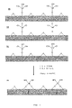
- Figure 4 Reaction scheme for ALD deposition of hafnium chloride and water on silicon oxide at 300°C.
- Figure 5 shows possible starting surface composition following 1-3 cycles of hafnium chloride and water at 300°C.
- 5D shows the result after the UV treatment.
- Figure 6 Difference in layer thickness measured by ellipsometry between the substrate surface exposed to UV irradiation and the substrate surface not exposed to UV irradiation.
- Figure 7 Leakage current versus distance from the center of the spot on the surface exposed to UV irradiation.
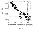
- Figure 8 EOT versus distance from the center of the spot on the surface exposed to UV irradiation.
- the invention provides an ALD method for depositing a layer comprising the steps of:
- an ALD method for depositing a layer comprising the steps of:
- a method according to the present invention can further comprise, between step (a) and step (b), and/or between step (b) and step (c), an additional step of providing an inert atmosphere in the reactor (i.e. an additional step (d)).
- said additional step of providing an inert atmosphere in the reactor is between step (b) and step (c).
- Said UV irradiation exposure can take place:
- step (d) of providing an inert atmosphere in the reactor is performed at least once (and preferably once) after step (c).
- step of providing an inert atmosphere in the reactor can also be further performed, at least once (and preferably once), between step (a) and step (b), and/or or preferably, at least once (and preferably once), between step (b) and step (c).
- the semiconductor substrate is exposed at least once to UV irradiation within a method of the invention, during a step (d).
- Said UV irradiation exposure can be done during the first step of providing said inert atmosphere, and/or any of the subsequent step(s) of providing said inert atmosphere.
- said UV irradiation exposure need not be repeated according to step (e), i.e. said UV irradiation exposure can be performed in one single ALD cycle. But said UV irradiation exposure is preferably repeated few times (e.g. 2, 3, 4, 5, 6, 7, 8 or 9), in particular up to 15 times, more preferably up to 10 times.
- said UV irradiation exposure can be repeated once the first few (e.g. 2, 3, 4, 5, 6, 7, 8, 9 or 10) deposition cycles.
- inert atmosphere can also be referred to as "inert gas”.
- the term "deposition cycle” or “ALD cycle” refers to a sequence of steps comprising step (b), step (c), and step (d).
- the semiconductor substrate can comprise or can consist of any semiconductor material(s) suitable in the field of IC processing, in particular silicon, silicon-on-insulator (SOI), germanium, germanium-on-insulator (GOI), all compound semiconductor substrates, or any combination thereof.
- semiconductor material(s) suitable in the field of IC processing in particular silicon, silicon-on-insulator (SOI), germanium, germanium-on-insulator (GOI), all compound semiconductor substrates, or any combination thereof.
- the deposited layer (more particularly the layer to be deposited) may be selected from the group consisting of oxides, such as but not limited to titanium oxide, tantalum oxide, aluminium oxide, zirconium oxide, lanthanum oxide, hafnium oxide, hafnium aluminum oxide, hafnium scandium oxide and hafnium silicon oxide, or any combination thereof.
- oxides such as but not limited to titanium oxide, tantalum oxide, aluminium oxide, zirconium oxide, lanthanum oxide, hafnium oxide, hafnium aluminum oxide, hafnium scandium oxide and hafnium silicon oxide, or any combination thereof.
- the layer may also be selected from the group consisting of oxynitrides, such as but not limited to titanium oxynitride, tantalum oxynitride, aluminium oxynitride, zirconium oxynitride, lanthanum oxynitride, hafnium oxynitride, hafnium scandium oxynitride, hafnium silicon oxynitride, or any combination thereof.
- oxynitrides such as but not limited to titanium oxynitride, tantalum oxynitride, aluminium oxynitride, zirconium oxynitride, lanthanum oxynitride, hafnium oxynitride, hafnium scandium oxynitride, hafnium silicon oxynitride, or any combination thereof.
- the first precursor gas may be selected from the group consisting of metal halides, oxyhalides and metalorganics (also called organometalics), such as hafnium chloride, tantalum chloride, tungsten chloride, zirconium chloride, aluminum chloride, tungsten oxychloride, phosphorous oxychloride, TEMA-Hf (tetrakis-ethyl-methyl-amino-hafnium) or TDEA-Hf (tetrakis-diethyl-amino-hafnium).
- metal halides also called organometalics
- metalorganics also called organometalics
- the second precursor gas can comprise or consist of a gas be selected from the group consisting of H 2 O, H 2 O 2 , O 2 , O 3 , and any precursor suitable for forming oxides or oxynitrides in combination with a first precursor.
- step b) through step d) may be done as many times as necessary to obtain the layer thickness wanted or required.
- any (UV) wavelength having enough irradiation energy to increase the dissociation of the first precursor and increase the formation of hydroxyls is envisaged. Since energy of irradiation increases with decreasing wavelength the shorter the wavelength the better, but this is of course dependent on the availability of suitable UV sources.
- the wavelength of the UV irradiation is preferably lower than 205 nanometer, lower than 200 nanometer, lower than 195 nanometer, lower than 190 nanometer, more preferably lower than 185 nanometer, even more preferably lower than 175 nanometer.
- the wavelength of the UV irradiation is comprised between (about) 205 nm and (about) 157 nm, preferably between (about) 195 nm and (about) 157 nm, more preferably between (about) 190 nm and (about) 157 nm, even more preferably between (about) 185 nm and (about) 157 nm.
- the inert atmosphere may be provided by purging an inert gas such as but not limited to nitrogen or argon into the reactor chamber.
- trace amounts of water, hydrogen peroxide, hydrogen or any other specie suitable for forming hydroxyls in combination with a first and second precursor may be present in the inert atmosphere.
- the semiconductor substrate can be exposed to heat during exposure to UV irradiation.
- the temperature may be between room temperature and about 350°C, between room temperature and about 300°C, between about 100°C and about 250°C, or between about 150°C and about 220°C.
- step a) through d) may be performed at a temperature between about 100°C and about 250°C, or between about 150°C and about 220°C.
- the exposure to UV irradiation is preferably stopped after 10, after 5, after 2 or after 1 deposition cycle(s), depending on the desired deposited layer quality.
- the number of deposition cycles including exposure to UV can influence the deposited layer quality.
- a method according the invention allows to dramatically improve both chemical and electrical properties of the ALD layer.
- the density of the layer is increased at the interface between the ALD layer and the semiconductor substrate with the impact of reducing defects at this interface and thus directly improving the layers electrical characteristics.
- the properties of a dielectric layer on a semiconductor substrate may be optimized and may allow the creation of a layer with superior electrical characteristics including significantly reduced defects in interface states and improved leakage performance.
- a layer according to a method of the invention after depositing a layer according to a method of the invention, there is no native oxide re-growth, such as silicon oxide or germanium oxide. Carrying out a method of the invention may actually offer protection towards regrowth during high temperature annealing.
- a method for depositing a HfO 2 layer comprising the steps of:
- a further nitrogen purge can be performed between step (a') and step (b'), and/or between step (b') and step (c').
- step (b') one further nitrogen purge is done between step (b') and step (c').
- Said UV irradiation exposure can be performed during any of the nitrogen purges, or during each and every one of them, or during any two of them.
- Said UV irradiation exposure need not be repeated according to step (e'), i.e. said UV irradiation exposure can be performed in one single ALD cycle.
- the ALD of hafnium chloride is performed at lower temperatures (than usually performed), in the range of 150°C-220°C (figure 1).
- the Si surface has a significantly higher concentration of surface hydroxyls than under the conventional deposition temperature of 300°C.
- the lower temperature has the negative side effect of not driving the HfCl 4 reaction to completion.
- the resulting species has some concentration of - OCl termination of the Hf instead of the more desirable -OH termination.
- the growth rate of the ALD can be nearly a monolayer ( ⁇ 0.2nm) per cycle, the defects introduced by the OCl terminations will make for a poor quality layer.
- the UV irradiation of the surface are performed with wavelengths shorter that 200 nm.
- the preferred wavelength is about 185 nm, but 193 nm may also suffice.
- the atmosphere is controlled so that the irradiation takes place in N 2 or noble gas atmosphere with trace amounts of water or hydrogen peroxide present, so as to drive the reaction to completion giving an OH termination of all available Hf sites.
- the temperature range is optimized between 100°C and 300° C.
- the ALD growth process can be continued at 300°C with alternating HfCl 4 and H 2 O water pulses.
- the ALD starts with the conventional process at 300°C but in this case the Si surface looks significantly different.
- Figure 3 shows a schematic of the Si surface at 300°C. One can clearly see the difference compared to the starting surface in figure 1.
- An ALD deposition is done on a silicon semiconductor substrate, starting from HCl 4 as first precursor and H 2 O as second precursor.
- an inert atmosphere is provided by purging the reactor with nitrogen.
- a nitrogen purge is also done after the H 2 O pulse.
- a spot of about 40mm width on the silicon substrate is then exposed to a 172 nm UV irradiation during one of the two nitrogen purges.
- the triangles(A) show the layer thickness after 10 cycles of conventional ALD without UV exposure.
- the dots(•) show the layer thickness after 10 cycles of conventional ALD deposition, followed by 3 min UV exposure as a post-deposition treatment.
- the diamonds( ⁇ ) show the layer thickness after 10 cycles of ALD including in each cycle, after the H 2 O pulse, an exposure to UV irradiation.
- the thickness is higher where the UV irradiation hit the substrate surface (between about 30 and 40 units of the wafer scan).
- the squares( ⁇ ) show the layer thickness after 10 cycles of ALD including in each cycle, after the HfCl 4 pulse, an exposure to UV irradiation.
- the thickness is higher where the UV irradiation hit the substrate surface (between about 30 and 40 units of the wafer scan).
- An exposure to UV as a post-deposition treatment shows no effect: the layer thickness is not increased where the UV irradiation hit the substrate surface.
- the overall increased layer thickness in the latter case is probably caused by exposure to moisture between the ALD and the post-deposition exposure to UV.
- Figure 7 shows that, with decreasing distance towards the center of the spot of the surface exposed to UV, the leakage current of the HfO 2 is decreasing.
- the gradient in leakage current is probably caused by the intensity gradient of the UV radiation source.
- EOT Equivalent Oxide Thickness
Landscapes
- Chemical & Material Sciences (AREA)
- Engineering & Computer Science (AREA)
- Materials Engineering (AREA)
- Organic Chemistry (AREA)
- General Chemical & Material Sciences (AREA)
- Chemical Kinetics & Catalysis (AREA)
- Mechanical Engineering (AREA)
- Metallurgy (AREA)
- Health & Medical Sciences (AREA)
- Toxicology (AREA)
- Physics & Mathematics (AREA)
- Optics & Photonics (AREA)
- Electromagnetism (AREA)
- Plasma & Fusion (AREA)
- Inorganic Chemistry (AREA)
- Formation Of Insulating Films (AREA)
- Chemical Vapour Deposition (AREA)
- Internal Circuitry In Semiconductor Integrated Circuit Devices (AREA)
- Electrodes Of Semiconductors (AREA)
Abstract
a) providing a semiconductor substrate in a reactor,
b) providing a pulse of a first precursor gas into the reactor,
c) providing a pulse of a second precursor gas into the reactor,
d) providing an inert atmosphere in the reactor,
e) repeating step b) through step d),
wherein at least once during step d) the semiconductor substrate is exposed to UV irradiation.
Description
- The invention relates to an improved ALD method for depositing layers in the field of semiconductor processing.
- The invention also relates to a semiconductor device obtainable by a method according to the invention.
- Because in the field of electronics in general further downscaling of the semiconductor devices is always proceeding, deposition processes have to be developed that are able to deposit layers with a thickness control at atomic layer scale. One of these deposition techniques is Atomic Layer Deposition (ALD), often used for depositing dielectric layers.
- In order to achieve satisfying semiconductor device characteristics the interface quality between the semiconductor substrate and the ALD layer has to be controlled sufficiently.
- Since for ALD processes the deposition is very temperature sensitive, this control of the interface quality is very challenging.
- One of the main reasons why ALD is temperature sensitive is that depending on temperature the semiconductor substrate always has a limited concentration of [OH] (hydroxyl) groups at the surface, which are the active sites for starting the ALD reaction cycle.
- Methods have been described intended for preparation of silicon surfaces with a concentration of [OH] at 5 x 1014 cm-2 before starting the HfCl4 ALD reaction cycle. If each of these reactive sites were utilized one could expect good interface formation. However, data from electrical evaluation of devices with high-k grown with a standard ALD process consequent to these surface preparation methods indicates poor interface quality.
- As mentioned above, it is known that the concentration of surface hydroxyls decreases with increasing temperature. Since the semiconductor substrate surface is at a temperature of 300°C during the conventional ALD deposition the [OH] concentration is limited.
- At lower temperature the silicon surface has a significantly higher concentration of surface hydroxyls than under the conventional deposition temperature of 300°C. However, the lower temperature has the negative side effect of not driving the ALD reaction cycle to completion.
- The present invention aims to provide an ALD method to improve the chemical and electrical characteristics of the deposited layer.
- An Atomic Layer Deposition (ALD) method for depositing a layer is provided, comprising the steps of:
- a) providing a semiconductor substrate in a reactor,
- b) providing a pulse of a first precursor gas into the reactor,
- c) providing a pulse of a second precursor gas into the reactor,
- d) providing an inert atmosphere in the reactor,
- e) repeating at least once step b) through step d), wherein the semiconductor substrate is exposed to ultraviolet (UV) irradiation at least once during a step (d).
- A method according to the present invention can further comprise, between step (a) and step (b), and/or between step (b) and step (c), an additional step of providing an inert atmosphere in the reactor. Preferably, one additional step of providing an inert atmosphere in the reactor is performed between step (b) and step (c).
- Said UV irradiation exposure can take place:
- during any one of these steps of providing an inert atmosphere in the reactor, or
- during each step of providing an inert atmosphere in the reactor, or
- during some (two or more) of these steps of providing an inert atmosphere in the reactor.
- In a method according to the invention, said UV irradiation exposure need not be repeated according to step (e), i.e. said UV irradiation exposure can be performed in one single ALD cycle.
- Said first precursor gas may be selected from the group consisting of metal halides, metal oxyhalides and metalorganics (also called organometalics), such as hafnium chloride, tantalum chloride, tungsten chloride, zirconium chloride, aluminum chloride, tungsten oxychloride, phosphorous oxychloride, TEMA-Hf (tetrakis-ethyl-methyl-amino-hafnium) or TDEA-Hf (tetrakis-diethyl-amino-hafnium).
- The second precursor gas can comprise or consist of any precursor suitable for forming oxides or oxynitrides in combination with said first precursor.
- Preferably, said second precursor gas comprises or consists of a gas selected from the group consisting of H2O, H2O2, O2, and O3.
- In a method according to the invention, any UV wavelength having enough irradiation energy to increase the dissociation of the first precursor and increase the formation of hydroxyls (when compared to a method without exposure of the semiconductor substrate to UV irradiation) is envisaged.
- Preferably, the wavelength of the UV irradiation is lower than (about) 205 nanometer, or lower than (about) 200 nanometer, preferably lower than (about) 195 nanometer, or lower than (about) 190 nanometer, and more preferably lower than (about) 185 nanometer, or lower than (about) 175 nanometer.
- More particularly, the wavelength of the UV irradiation is comprised between (about) 205 nm and (about) 157 nm, preferably between (about) 195 nm and (about) 157 nm, more preferably between (about) 190 nm and (about) 157 nm, even more preferably between (about) 185 nm and (about) 157 nm.
- In a method according to the invention, the inert atmosphere may be provided by purging an inert gas into the reactor chamber, such as a noble gas or nitrogen, preferably by purging nitrogen into the reactor chamber.
- In a method according to the invention, trace amounts of water, hydrogen peroxide, hydrogen or any other specie suitable for forming hydroxyls in combination with a first and second precursor may be present in the inert atmosphere.
- In a method according to the invention, the semiconductor substrate can be exposed to heat (can be heated) during exposure to UV irradiation (i.e. during the UV irradiation treatment).
- The temperature may be comprised between room temperature and (about) 350°C, preferably between room temperature and (about) 300°C, more preferably between (about) 100°C and (about) 250°C, or even more preferably between (about) 150°C and (about) 220°C.
- In a method according to the invention, step (a) through (d) may be performed at a temperature between (about) 100°C and (about) 250°C, or preferably between (about) 150° and (about) 220°C.
- In a method according to the invention, the exposure to UV irradiation can be stopped after 15 deposition cycles, after 10 deposition cycles, after 5 deposition cycles, after 2 deposition cycles or after 1 deposition cycle.
- In a method according to the invention, the semiconductor substrate is preferably exposed up to 15 times, preferably up to 10 times to UV irradiation. Said semiconductor substrate can be exposed only once, or 2, 3, 4 or 5 times.
- Said UV irradiation exposure preferably varies from few seconds (e.g. from about 2 or 3 sec. to about 100 sec.) to few minutes (e.g. between about 2 min. to about 10 min., preferably between about 2 min. and about 5 min, more preferably about 3 min.).
- Figure 1: Result from hafnium chloride reaction with water at low temperatures.
- Figure 2: Result of exposure of initial treated ALD surface with UV for low temperature ALD.
- Figure 3: Projected silicon surface structure at 300°C.
- Figure 4: Reaction scheme for ALD deposition of hafnium chloride and water on silicon oxide at 300°C.
- Figure 5: 5A-5C shows possible starting surface composition following 1-3 cycles of hafnium chloride and water at 300°C. 5D shows the result after the UV treatment.
- Figure 6: Difference in layer thickness measured by ellipsometry between the substrate surface exposed to UV irradiation and the substrate surface not exposed to UV irradiation.
- Figure 7: Leakage current versus distance from the center of the spot on the surface exposed to UV irradiation.
- Figure 8: EOT versus distance from the center of the spot on the surface exposed to UV irradiation.
- The invention provides an ALD method for depositing a layer comprising the steps of:
- a) providing a semiconductor substrate in a reactor,
- b) providing a pulse of a first precursor gas into the reactor,
- c) providing a pulse of a second precursor gas into the reactor,
- d) providing an inert atmosphere in the reactor,
- e) repeating step a) through step d),
- More particularly, an ALD method for depositing a layer is provided, comprising the steps of:
- a) providing a semiconductor substrate in a reactor,
- b) providing a pulse of a first precursor gas into the reactor,
- c) providing a pulse of a second precursor gas into the reactor,
- d) providing an inert atmosphere in the reactor,
- e) repeating at least once step b) through step d),
- A method according to the present invention can further comprise, between step (a) and step (b), and/or between step (b) and step (c), an additional step of providing an inert atmosphere in the reactor (i.e. an additional step (d)). Preferably, said additional step of providing an inert atmosphere in the reactor is between step (b) and step (c).
- Said UV irradiation exposure can take place:
- during any one of these steps of providing an inert atmosphere in the reactor, or
- during each (and every) step of providing an inert atmosphere in the reactor, or
- during some (two, or if possible three or more) of these steps of providing an inert atmosphere in the reactor.
- In other words, in a method according to the invention, and within one deposition cycle, step (d) of providing an inert atmosphere in the reactor is performed at least once (and preferably once) after step (c). But said step of providing an inert atmosphere in the reactor can also be further performed, at least once (and preferably once), between step (a) and step (b), and/or or preferably, at least once (and preferably once), between step (b) and step (c).
- The semiconductor substrate is exposed at least once to UV irradiation within a method of the invention, during a step (d).
- Said UV irradiation exposure (or treatment) can be done during the first step of providing said inert atmosphere, and/or any of the subsequent step(s) of providing said inert atmosphere.
- In a method according to the invention, said UV irradiation exposure need not be repeated according to step (e), i.e. said UV irradiation exposure can be performed in one single ALD cycle. But said UV irradiation exposure is preferably repeated few times (e.g. 2, 3, 4, 5, 6, 7, 8 or 9), in particular up to 15 times, more preferably up to 10 times.
- For example, said UV irradiation exposure can be repeated once the first few (e.g. 2, 3, 4, 5, 6, 7, 8, 9 or 10) deposition cycles.
- In the context of the present invention, the term "inert atmosphere" can also be referred to as "inert gas".
- In the context of the present invention, the term "deposition cycle" or "ALD cycle" refers to a sequence of steps comprising step (b), step (c), and step (d).
- The aspects and advantages of the present invention will become apparent to those of ordinary skill in the art by reading the following detailed description, with reference where appropriate to the accompanying drawings.
- The semiconductor substrate can comprise or can consist of any semiconductor material(s) suitable in the field of IC processing, in particular silicon, silicon-on-insulator (SOI), germanium, germanium-on-insulator (GOI), all compound semiconductor substrates, or any combination thereof.
- The deposited layer (more particularly the layer to be deposited) may be selected from the group consisting of oxides, such as but not limited to titanium oxide, tantalum oxide, aluminium oxide, zirconium oxide, lanthanum oxide, hafnium oxide, hafnium aluminum oxide, hafnium scandium oxide and hafnium silicon oxide, or any combination thereof.
- The layer may also be selected from the group consisting of oxynitrides, such as but not limited to titanium oxynitride, tantalum oxynitride, aluminium oxynitride, zirconium oxynitride, lanthanum oxynitride, hafnium oxynitride, hafnium scandium oxynitride, hafnium silicon oxynitride, or any combination thereof.
- The first precursor gas may be selected from the group consisting of metal halides, oxyhalides and metalorganics (also called organometalics), such as hafnium chloride, tantalum chloride, tungsten chloride, zirconium chloride, aluminum chloride, tungsten oxychloride, phosphorous oxychloride, TEMA-Hf (tetrakis-ethyl-methyl-amino-hafnium) or TDEA-Hf (tetrakis-diethyl-amino-hafnium).
- The second precursor gas can comprise or consist of a gas be selected from the group consisting of H2O, H2O2, O2, O3, and any precursor suitable for forming oxides or oxynitrides in combination with a first precursor.
- Repeating step b) through step d) may be done as many times as necessary to obtain the layer thickness wanted or required.
- In a method according to the invention, any (UV) wavelength having enough irradiation energy to increase the dissociation of the first precursor and increase the formation of hydroxyls (compared to any method without exposure of the semiconductor substrate to UV irradiation) is envisaged. Since energy of irradiation increases with decreasing wavelength the shorter the wavelength the better, but this is of course dependent on the availability of suitable UV sources.
- In a method according to the invention, the wavelength of the UV irradiation is preferably lower than 205 nanometer, lower than 200 nanometer, lower than 195 nanometer, lower than 190 nanometer, more preferably lower than 185 nanometer, even more preferably lower than 175 nanometer.
- More particularly, the wavelength of the UV irradiation is comprised between (about) 205 nm and (about) 157 nm, preferably between (about) 195 nm and (about) 157 nm, more preferably between (about) 190 nm and (about) 157 nm, even more preferably between (about) 185 nm and (about) 157 nm.
- In a method according to the invention, the inert atmosphere may be provided by purging an inert gas such as but not limited to nitrogen or argon into the reactor chamber.
- In a method according to the invention, trace amounts of water, hydrogen peroxide, hydrogen or any other specie suitable for forming hydroxyls in combination with a first and second precursor may be present in the inert atmosphere.
- In a method according to the invention, the semiconductor substrate can be exposed to heat during exposure to UV irradiation.
- The temperature may be between room temperature and about 350°C, between room temperature and about 300°C, between about 100°C and about 250°C, or between about 150°C and about 220°C.
- In a method according to the invention step a) through d) may be performed at a temperature between about 100°C and about 250°C, or between about 150°C and about 220°C.
- In a method according to the invention, the exposure to UV irradiation is preferably stopped after 10, after 5, after 2 or after 1 deposition cycle(s), depending on the desired deposited layer quality.
- Indeed, the number of deposition cycles including exposure to UV can influence the deposited layer quality.
- A method according the invention allows to dramatically improve both chemical and electrical properties of the ALD layer.
- Specifically, the density of the layer is increased at the interface between the ALD layer and the semiconductor substrate with the impact of reducing defects at this interface and thus directly improving the layers electrical characteristics.
- More specifically, the properties of a dielectric layer on a semiconductor substrate may be optimized and may allow the creation of a layer with superior electrical characteristics including significantly reduced defects in interface states and improved leakage performance.
- Furthermore, in some cases, after depositing a layer according to a method of the invention, there is no native oxide re-growth, such as silicon oxide or germanium oxide. Carrying out a method of the invention may actually offer protection towards regrowth during high temperature annealing.
- According to a preferred embodiment, a method is provided for depositing a HfO2 layer, comprising the steps of:
- a') providing a semiconductor substrate in a reactor, preferably a Si substrate,
- b') providing a pulse of a HfC14 gas into the reactor,
- c') providing a pulse of a H2O gas into the reactor,
- d') purging the reactor with a nitrogen gas,
- e') repeating at least once step (b') through step (d'),
- In said preferred embodiment, a further nitrogen purge can be performed between step (a') and step (b'), and/or between step (b') and step (c').
- Preferably, one further nitrogen purge is done between step (b') and step (c').
- Said UV irradiation exposure (or treatment) can be performed during any of the nitrogen purges, or during each and every one of them, or during any two of them.
- Said UV irradiation exposure need not be repeated according to step (e'), i.e. said UV irradiation exposure can be performed in one single ALD cycle.
- For said preferred embodiment, all the features mentioned for the invention described in its broadest acception are also envisaged, where the case may be.
- As a first example of the invention, the ALD of hafnium chloride is performed at lower temperatures (than usually performed), in the range of 150°C-220°C (figure 1).
- At these temperatures, the Si surface has a significantly higher concentration of surface hydroxyls than under the conventional deposition temperature of 300°C.
- However, the lower temperature has the negative side effect of not driving the HfCl4 reaction to completion.
- The resulting species has some concentration of - OCl termination of the Hf instead of the more desirable -OH termination.
- So, although the growth rate of the ALD can be nearly a monolayer (~0.2nm) per cycle, the defects introduced by the OCl terminations will make for a poor quality layer.
- Additionally, it is difficult to remove the residual Cl out of the layers through post deposition anneals.
- When treating (exposing) the semiconductor substrate with UV in the first one to five cycles, dissociation of HfCl4 is increased and Cl is driven off, thereby leaving a HfO2 lattice terminated by OH groups. Figure 2 shows the reaction scheme.
- The UV irradiation of the surface are performed with wavelengths shorter that 200 nm.
- The preferred wavelength is about 185 nm, but 193 nm may also suffice.
- The atmosphere is controlled so that the irradiation takes place in N2 or noble gas atmosphere with trace amounts of water or hydrogen peroxide present, so as to drive the reaction to completion giving an OH termination of all available Hf sites.
- Additionally heat is added to optimize the reaction during irradiation with UV light. The temperature range is optimized between 100°C and 300° C.
- Organic species have to be carefully excluded from the system, as this will introduce significant contamination to the deposited layer.
- After this initial layer has been formed the ALD growth process can be continued at 300°C with alternating HfCl4 and H2O water pulses.
- As a second example of the invention, the ALD starts with the conventional process at 300°C but in this case the Si surface looks significantly different.
- Figure 3 shows a schematic of the Si surface at 300°C. One can clearly see the difference compared to the starting surface in figure 1.
- With this high temperature, adjacent hydroxyls react as shown in figure 4, leaving few isolated OH groups.
- This dramatically reduces the surface coverage in the first few cycles of the ALD process.
- In figure 5A-C, possible starting surface compositions following 1-3 cycles of HfCl4 and H2O are illustrated. After UV treatment (figure 5D) the surface coverage is increased dramatically.
- An ALD deposition is done on a silicon semiconductor substrate, starting from HCl4 as first precursor and H2O as second precursor.
- Between the HCl4 pulse and the H2O pulse an inert atmosphere is provided by purging the reactor with nitrogen.
- A nitrogen purge is also done after the H2O pulse.
- A spot of about 40mm width on the silicon substrate is then exposed to a 172 nm UV irradiation during one of the two nitrogen purges.
- In figure 6, the difference in layer thickness measured by ellipsometry between the substrate surface exposed to UV irradiation and the substrate surface not exposed to UV irradiation is shown.
- The triangles(A) show the layer thickness after 10 cycles of conventional ALD without UV exposure.
- The dots(•) show the layer thickness after 10 cycles of conventional ALD deposition, followed by 3 min UV exposure as a post-deposition treatment.
- The diamonds(◆) show the layer thickness after 10 cycles of ALD including in each cycle, after the H2O pulse, an exposure to UV irradiation.
- One can clearly see that the thickness is higher where the UV irradiation hit the substrate surface (between about 30 and 40 units of the wafer scan).
- The squares(■) show the layer thickness after 10 cycles of ALD including in each cycle, after the HfCl4 pulse, an exposure to UV irradiation.
- Again, one can clearly see that the thickness is higher where the UV irradiation hit the substrate surface (between about 30 and 40 units of the wafer scan).
- One can conclude that exposure to UV included in each ALD cycle results in increased layer thickness.
- An exposure to UV as a post-deposition treatment shows no effect: the layer thickness is not increased where the UV irradiation hit the substrate surface.
- The overall increased layer thickness in the latter case is probably caused by exposure to moisture between the ALD and the post-deposition exposure to UV.
- Figure 7 shows that, with decreasing distance towards the center of the spot of the surface exposed to UV, the leakage current of the HfO2 is decreasing. The gradient in leakage current is probably caused by the intensity gradient of the UV radiation source.
- At the same time, the Equivalent Oxide Thickness (EOT) is increasing with decreasing distance towards the center of the spot on the surface exposed to UV (figure 8). Again the gradient in EOT is probably caused by the intensity gradient of the UV radiation source.
- From both figures, one could conclude that the quality of the ALD HfO2 layer increases by exposure to UV irradiation.
Claims (20)
- An ALD method for depositing a layer comprising the steps of:a) providing a semiconductor substrate in a reactor,b) providing a pulse of a first precursor gas into the reactor,c) providing a pulse of a second precursor gas into the reactor,d) providing an inert atmosphere in the reactor,e) repeating at least once step b) through step d),wherein the semiconductor substrate is exposed to UV irradiation at least once during a step (d).
- A method according to claim 1, further comprising, between step (a) and step (b), and/or between step (b) and step (c), a step of providing an inert atmosphere in the reactor.
- A method according to claim 1 or 2, wherein said UV irradiation exposure is performed during any one of these steps of providing an inert atmosphere in the reactor.
- A method according to claim 1 or 2, wherein said UV irradiation exposure is performed during some (two or more) of these steps of providing an inert atmosphere in the reactor.
- A method according to claim 1 or 2, wherein said UV irradiation exposure is performed during each step of providing an inert atmosphere in the reactor.
- A method according to any of claims 1 to 5, wherein said first precursor gas is selected from the group consisting of metal halides, metal oxyhalides and metalorganics.
- A method according to any of claims 1 to 6, wherein said second precursor gas comprises or consists of a gas selected from the group consisting of any precursor suitable for forming oxides or oxynitrides in combination with said first precursor.
- A method according to claim 7, wherein said gas is selected from the group consisting of H2O, H2O2, O2 and O3.
- A method according to any of claims 1 to 8, wherein the wavelength of the UV irradiation is selected to provide sufficient energy to increase the dissociation of the first precursor and increase the formation of hydroxyls compared to the same method without exposure of the semiconductor substrate to UV irradiation.
- A method according to claim 9, wherein the wavelength of the UV irradiation is lower than 205 nm, lower than 195 nm, lower than 185 nm, lower than 175 nm.
- A method according to any of claims 1 to 10, wherein said inert atmosphere is provided by purging an inert gas such as a noble gas or nitrogen.
- A method according to any of claims 1 to 11, wherein trace amounts of water, hydrogen peroxide, hydrogen or any other specie suitable for forming hydroxyls in combination with a first and second precursor are present in said inert atmosphere.
- A method according to any of claims 1 to 12, wherein said semiconductor substrate is exposed to heat during exposure to UV irradiation, the temperature varying between about room temperature and about 350°C.
- A method according to any of claims 1 to 13, wherein step b) through d) are performed at a temperature between about 100°C and about 250°C, or between about 150°C and about 220°C.
- A method according to any of claims 1 to 14, wherein the exposure to UV irradiation is stopped after 10, after 5, after 2 or after 1 deposition cycle(s).
- A method according to any of claims 1 to 15, wherein the semiconductor substrate is exposed 10 times, 5 times, 2 times or once to UV irradiation.
- A method according to any of claims 1 to 16, wherein said semiconductor substrate consists of Si, silicon-on-insulator, Ge, or germanium-on-insulator, or any combination thereof.
- A method according to any of claims 1 to 17, wherein said first precursor of HfCl4, and said second precursor of H2O, whereby the layer deposited is HfO2.
- A method according to any of claims 1 to 18, wherein said inert gas in nitrogen.
- A semiconductor device obtainable by a method according to any of claims 1 to 19.
Applications Claiming Priority (1)
| Application Number | Priority Date | Filing Date | Title |
|---|---|---|---|
| US69833105P | 2005-07-11 | 2005-07-11 |
Publications (2)
| Publication Number | Publication Date |
|---|---|
| EP1743954A1 true EP1743954A1 (en) | 2007-01-17 |
| EP1743954B1 EP1743954B1 (en) | 2010-05-12 |
Family
ID=37059999
Family Applications (1)
| Application Number | Title | Priority Date | Filing Date |
|---|---|---|---|
| EP06116996A Active EP1743954B1 (en) | 2005-07-11 | 2006-07-11 | An ALD method for depositing a layer |
Country Status (5)
| Country | Link |
|---|---|
| US (1) | US7579285B2 (en) |
| EP (1) | EP1743954B1 (en) |
| JP (1) | JP2007027723A (en) |
| AT (1) | ATE467700T1 (en) |
| DE (1) | DE602006014233D1 (en) |
Families Citing this family (370)
| Publication number | Priority date | Publication date | Assignee | Title |
|---|---|---|---|---|
| KR100877100B1 (en) * | 2007-04-16 | 2009-01-09 | 주식회사 하이닉스반도체 | Nonvolatile Memory Device Manufacturing Method |
| US7939932B2 (en) * | 2007-06-20 | 2011-05-10 | Analog Devices, Inc. | Packaged chip devices with atomic layer deposition protective films |
| US8283258B2 (en) | 2007-08-16 | 2012-10-09 | Micron Technology, Inc. | Selective wet etching of hafnium aluminum oxide films |
| JP5208128B2 (en) * | 2007-12-04 | 2013-06-12 | フルテック株式会社 | Pressurized gas pulse control processing method and pressurized gas pulse control processing apparatus |
| US10378106B2 (en) | 2008-11-14 | 2019-08-13 | Asm Ip Holding B.V. | Method of forming insulation film by modified PEALD |
| US20100183825A1 (en) * | 2008-12-31 | 2010-07-22 | Cambridge Nanotech Inc. | Plasma atomic layer deposition system and method |
| US9394608B2 (en) | 2009-04-06 | 2016-07-19 | Asm America, Inc. | Semiconductor processing reactor and components thereof |
| US8802201B2 (en) | 2009-08-14 | 2014-08-12 | Asm America, Inc. | Systems and methods for thin-film deposition of metal oxides using excited nitrogen-oxygen species |
| US9312155B2 (en) | 2011-06-06 | 2016-04-12 | Asm Japan K.K. | High-throughput semiconductor-processing apparatus equipped with multiple dual-chamber modules |
| US10364496B2 (en) | 2011-06-27 | 2019-07-30 | Asm Ip Holding B.V. | Dual section module having shared and unshared mass flow controllers |
| US10854498B2 (en) | 2011-07-15 | 2020-12-01 | Asm Ip Holding B.V. | Wafer-supporting device and method for producing same |
| US20130023129A1 (en) | 2011-07-20 | 2013-01-24 | Asm America, Inc. | Pressure transmitter for a semiconductor processing environment |
| US9017481B1 (en) | 2011-10-28 | 2015-04-28 | Asm America, Inc. | Process feed management for semiconductor substrate processing |
| JP5842750B2 (en) | 2012-06-29 | 2016-01-13 | 東京エレクトロン株式会社 | Film forming method, film forming apparatus, and storage medium |
| US9659799B2 (en) | 2012-08-28 | 2017-05-23 | Asm Ip Holding B.V. | Systems and methods for dynamic semiconductor process scheduling |
| US10714315B2 (en) | 2012-10-12 | 2020-07-14 | Asm Ip Holdings B.V. | Semiconductor reaction chamber showerhead |
| US20160376700A1 (en) | 2013-02-01 | 2016-12-29 | Asm Ip Holding B.V. | System for treatment of deposition reactor |
| US9484191B2 (en) | 2013-03-08 | 2016-11-01 | Asm Ip Holding B.V. | Pulsed remote plasma method and system |
| US9589770B2 (en) | 2013-03-08 | 2017-03-07 | Asm Ip Holding B.V. | Method and systems for in-situ formation of intermediate reactive species |
| US20150064361A1 (en) * | 2013-09-04 | 2015-03-05 | Intermolecular Inc. | UV treatment for ALD film densification |
| US9240412B2 (en) | 2013-09-27 | 2016-01-19 | Asm Ip Holding B.V. | Semiconductor structure and device and methods of forming same using selective epitaxial process |
| US10683571B2 (en) | 2014-02-25 | 2020-06-16 | Asm Ip Holding B.V. | Gas supply manifold and method of supplying gases to chamber using same |
| SG11201605374UA (en) * | 2014-03-04 | 2016-09-29 | Picosun Oy | Atomic layer deposition of germanium or germanium oxide |
| US10167557B2 (en) | 2014-03-18 | 2019-01-01 | Asm Ip Holding B.V. | Gas distribution system, reactor including the system, and methods of using the same |
| US11015245B2 (en) | 2014-03-19 | 2021-05-25 | Asm Ip Holding B.V. | Gas-phase reactor and system having exhaust plenum and components thereof |
| US10858737B2 (en) | 2014-07-28 | 2020-12-08 | Asm Ip Holding B.V. | Showerhead assembly and components thereof |
| US9890456B2 (en) | 2014-08-21 | 2018-02-13 | Asm Ip Holding B.V. | Method and system for in situ formation of gas-phase compounds |
| US9657845B2 (en) | 2014-10-07 | 2017-05-23 | Asm Ip Holding B.V. | Variable conductance gas distribution apparatus and method |
| US10941490B2 (en) | 2014-10-07 | 2021-03-09 | Asm Ip Holding B.V. | Multiple temperature range susceptor, assembly, reactor and system including the susceptor, and methods of using the same |
| KR102263121B1 (en) | 2014-12-22 | 2021-06-09 | 에이에스엠 아이피 홀딩 비.브이. | Semiconductor device and manufacuring method thereof |
| US10529542B2 (en) | 2015-03-11 | 2020-01-07 | Asm Ip Holdings B.V. | Cross-flow reactor and method |
| US10276355B2 (en) | 2015-03-12 | 2019-04-30 | Asm Ip Holding B.V. | Multi-zone reactor, system including the reactor, and method of using the same |
| US10458018B2 (en) | 2015-06-26 | 2019-10-29 | Asm Ip Holding B.V. | Structures including metal carbide material, devices including the structures, and methods of forming same |
| US10600673B2 (en) | 2015-07-07 | 2020-03-24 | Asm Ip Holding B.V. | Magnetic susceptor to baseplate seal |
| US9960072B2 (en) | 2015-09-29 | 2018-05-01 | Asm Ip Holding B.V. | Variable adjustment for precise matching of multiple chamber cavity housings |
| US10211308B2 (en) | 2015-10-21 | 2019-02-19 | Asm Ip Holding B.V. | NbMC layers |
| US10322384B2 (en) | 2015-11-09 | 2019-06-18 | Asm Ip Holding B.V. | Counter flow mixer for process chamber |
| US11139308B2 (en) | 2015-12-29 | 2021-10-05 | Asm Ip Holding B.V. | Atomic layer deposition of III-V compounds to form V-NAND devices |
| US10468251B2 (en) | 2016-02-19 | 2019-11-05 | Asm Ip Holding B.V. | Method for forming spacers using silicon nitride film for spacer-defined multiple patterning |
| US10529554B2 (en) | 2016-02-19 | 2020-01-07 | Asm Ip Holding B.V. | Method for forming silicon nitride film selectively on sidewalls or flat surfaces of trenches |
| US10501866B2 (en) | 2016-03-09 | 2019-12-10 | Asm Ip Holding B.V. | Gas distribution apparatus for improved film uniformity in an epitaxial system |
| US10343920B2 (en) | 2016-03-18 | 2019-07-09 | Asm Ip Holding B.V. | Aligned carbon nanotubes |
| US9892913B2 (en) | 2016-03-24 | 2018-02-13 | Asm Ip Holding B.V. | Radial and thickness control via biased multi-port injection settings |
| US10190213B2 (en) | 2016-04-21 | 2019-01-29 | Asm Ip Holding B.V. | Deposition of metal borides |
| US10865475B2 (en) | 2016-04-21 | 2020-12-15 | Asm Ip Holding B.V. | Deposition of metal borides and silicides |
| US10032628B2 (en) | 2016-05-02 | 2018-07-24 | Asm Ip Holding B.V. | Source/drain performance through conformal solid state doping |
| US10367080B2 (en) | 2016-05-02 | 2019-07-30 | Asm Ip Holding B.V. | Method of forming a germanium oxynitride film |
| KR102592471B1 (en) | 2016-05-17 | 2023-10-20 | 에이에스엠 아이피 홀딩 비.브이. | Method of forming metal interconnection and method of fabricating semiconductor device using the same |
| US11453943B2 (en) | 2016-05-25 | 2022-09-27 | Asm Ip Holding B.V. | Method for forming carbon-containing silicon/metal oxide or nitride film by ALD using silicon precursor and hydrocarbon precursor |
| US10388509B2 (en) | 2016-06-28 | 2019-08-20 | Asm Ip Holding B.V. | Formation of epitaxial layers via dislocation filtering |
| US9859151B1 (en) | 2016-07-08 | 2018-01-02 | Asm Ip Holding B.V. | Selective film deposition method to form air gaps |
| US10612137B2 (en) | 2016-07-08 | 2020-04-07 | Asm Ip Holdings B.V. | Organic reactants for atomic layer deposition |
| US10714385B2 (en) | 2016-07-19 | 2020-07-14 | Asm Ip Holding B.V. | Selective deposition of tungsten |
| US10381226B2 (en) | 2016-07-27 | 2019-08-13 | Asm Ip Holding B.V. | Method of processing substrate |
| US10395919B2 (en) | 2016-07-28 | 2019-08-27 | Asm Ip Holding B.V. | Method and apparatus for filling a gap |
| KR102532607B1 (en) | 2016-07-28 | 2023-05-15 | 에이에스엠 아이피 홀딩 비.브이. | Substrate processing apparatus and method of operating the same |
| US9812320B1 (en) | 2016-07-28 | 2017-11-07 | Asm Ip Holding B.V. | Method and apparatus for filling a gap |
| US9887082B1 (en) | 2016-07-28 | 2018-02-06 | Asm Ip Holding B.V. | Method and apparatus for filling a gap |
| US10410943B2 (en) | 2016-10-13 | 2019-09-10 | Asm Ip Holding B.V. | Method for passivating a surface of a semiconductor and related systems |
| US10643826B2 (en) | 2016-10-26 | 2020-05-05 | Asm Ip Holdings B.V. | Methods for thermally calibrating reaction chambers |
| US11532757B2 (en) | 2016-10-27 | 2022-12-20 | Asm Ip Holding B.V. | Deposition of charge trapping layers |
| US10229833B2 (en) | 2016-11-01 | 2019-03-12 | Asm Ip Holding B.V. | Methods for forming a transition metal nitride film on a substrate by atomic layer deposition and related semiconductor device structures |
| US10643904B2 (en) | 2016-11-01 | 2020-05-05 | Asm Ip Holdings B.V. | Methods for forming a semiconductor device and related semiconductor device structures |
| US10714350B2 (en) | 2016-11-01 | 2020-07-14 | ASM IP Holdings, B.V. | Methods for forming a transition metal niobium nitride film on a substrate by atomic layer deposition and related semiconductor device structures |
| US10435790B2 (en) | 2016-11-01 | 2019-10-08 | Asm Ip Holding B.V. | Method of subatmospheric plasma-enhanced ALD using capacitively coupled electrodes with narrow gap |
| US10134757B2 (en) | 2016-11-07 | 2018-11-20 | Asm Ip Holding B.V. | Method of processing a substrate and a device manufactured by using the method |
| KR102546317B1 (en) | 2016-11-15 | 2023-06-21 | 에이에스엠 아이피 홀딩 비.브이. | Gas supply unit and substrate processing apparatus including the same |
| US10340135B2 (en) | 2016-11-28 | 2019-07-02 | Asm Ip Holding B.V. | Method of topologically restricted plasma-enhanced cyclic deposition of silicon or metal nitride |
| KR102762543B1 (en) | 2016-12-14 | 2025-02-05 | 에이에스엠 아이피 홀딩 비.브이. | Substrate processing apparatus |
| US11447861B2 (en) | 2016-12-15 | 2022-09-20 | Asm Ip Holding B.V. | Sequential infiltration synthesis apparatus and a method of forming a patterned structure |
| US11581186B2 (en) | 2016-12-15 | 2023-02-14 | Asm Ip Holding B.V. | Sequential infiltration synthesis apparatus |
| KR102700194B1 (en) | 2016-12-19 | 2024-08-28 | 에이에스엠 아이피 홀딩 비.브이. | Substrate processing apparatus |
| US10269558B2 (en) | 2016-12-22 | 2019-04-23 | Asm Ip Holding B.V. | Method of forming a structure on a substrate |
| US10867788B2 (en) | 2016-12-28 | 2020-12-15 | Asm Ip Holding B.V. | Method of forming a structure on a substrate |
| US11390950B2 (en) | 2017-01-10 | 2022-07-19 | Asm Ip Holding B.V. | Reactor system and method to reduce residue buildup during a film deposition process |
| TW201831720A (en) * | 2017-01-16 | 2018-09-01 | 美商精微超科技公司 | Methods of forming mld films using polyols with long carbon backbones |
| US10655221B2 (en) | 2017-02-09 | 2020-05-19 | Asm Ip Holding B.V. | Method for depositing oxide film by thermal ALD and PEALD |
| US10468261B2 (en) | 2017-02-15 | 2019-11-05 | Asm Ip Holding B.V. | Methods for forming a metallic film on a substrate by cyclical deposition and related semiconductor device structures |
| US10529563B2 (en) | 2017-03-29 | 2020-01-07 | Asm Ip Holdings B.V. | Method for forming doped metal oxide films on a substrate by cyclical deposition and related semiconductor device structures |
| US10283353B2 (en) | 2017-03-29 | 2019-05-07 | Asm Ip Holding B.V. | Method of reforming insulating film deposited on substrate with recess pattern |
| US10103040B1 (en) | 2017-03-31 | 2018-10-16 | Asm Ip Holding B.V. | Apparatus and method for manufacturing a semiconductor device |
| KR102457289B1 (en) | 2017-04-25 | 2022-10-21 | 에이에스엠 아이피 홀딩 비.브이. | Method for depositing a thin film and manufacturing a semiconductor device |
| US10770286B2 (en) | 2017-05-08 | 2020-09-08 | Asm Ip Holdings B.V. | Methods for selectively forming a silicon nitride film on a substrate and related semiconductor device structures |
| US10446393B2 (en) | 2017-05-08 | 2019-10-15 | Asm Ip Holding B.V. | Methods for forming silicon-containing epitaxial layers and related semiconductor device structures |
| US10892156B2 (en) | 2017-05-08 | 2021-01-12 | Asm Ip Holding B.V. | Methods for forming a silicon nitride film on a substrate and related semiconductor device structures |
| US10504742B2 (en) | 2017-05-31 | 2019-12-10 | Asm Ip Holding B.V. | Method of atomic layer etching using hydrogen plasma |
| US10886123B2 (en) | 2017-06-02 | 2021-01-05 | Asm Ip Holding B.V. | Methods for forming low temperature semiconductor layers and related semiconductor device structures |
| US12040200B2 (en) | 2017-06-20 | 2024-07-16 | Asm Ip Holding B.V. | Semiconductor processing apparatus and methods for calibrating a semiconductor processing apparatus |
| US11306395B2 (en) | 2017-06-28 | 2022-04-19 | Asm Ip Holding B.V. | Methods for depositing a transition metal nitride film on a substrate by atomic layer deposition and related deposition apparatus |
| US10685834B2 (en) | 2017-07-05 | 2020-06-16 | Asm Ip Holdings B.V. | Methods for forming a silicon germanium tin layer and related semiconductor device structures |
| KR20190009245A (en) | 2017-07-18 | 2019-01-28 | 에이에스엠 아이피 홀딩 비.브이. | Methods for forming a semiconductor device structure and related semiconductor device structures |
| US11374112B2 (en) | 2017-07-19 | 2022-06-28 | Asm Ip Holding B.V. | Method for depositing a group IV semiconductor and related semiconductor device structures |
| US11018002B2 (en) | 2017-07-19 | 2021-05-25 | Asm Ip Holding B.V. | Method for selectively depositing a Group IV semiconductor and related semiconductor device structures |
| US10541333B2 (en) | 2017-07-19 | 2020-01-21 | Asm Ip Holding B.V. | Method for depositing a group IV semiconductor and related semiconductor device structures |
| US10605530B2 (en) | 2017-07-26 | 2020-03-31 | Asm Ip Holding B.V. | Assembly of a liner and a flange for a vertical furnace as well as the liner and the vertical furnace |
| US10312055B2 (en) | 2017-07-26 | 2019-06-04 | Asm Ip Holding B.V. | Method of depositing film by PEALD using negative bias |
| US10590535B2 (en) | 2017-07-26 | 2020-03-17 | Asm Ip Holdings B.V. | Chemical treatment, deposition and/or infiltration apparatus and method for using the same |
| TWI815813B (en) | 2017-08-04 | 2023-09-21 | 荷蘭商Asm智慧財產控股公司 | Showerhead assembly for distributing a gas within a reaction chamber |
| US10692741B2 (en) | 2017-08-08 | 2020-06-23 | Asm Ip Holdings B.V. | Radiation shield |
| US10770336B2 (en) | 2017-08-08 | 2020-09-08 | Asm Ip Holding B.V. | Substrate lift mechanism and reactor including same |
| US11769682B2 (en) | 2017-08-09 | 2023-09-26 | Asm Ip Holding B.V. | Storage apparatus for storing cassettes for substrates and processing apparatus equipped therewith |
| US10249524B2 (en) | 2017-08-09 | 2019-04-02 | Asm Ip Holding B.V. | Cassette holder assembly for a substrate cassette and holding member for use in such assembly |
| US11139191B2 (en) | 2017-08-09 | 2021-10-05 | Asm Ip Holding B.V. | Storage apparatus for storing cassettes for substrates and processing apparatus equipped therewith |
| USD900036S1 (en) | 2017-08-24 | 2020-10-27 | Asm Ip Holding B.V. | Heater electrical connector and adapter |
| US11830730B2 (en) | 2017-08-29 | 2023-11-28 | Asm Ip Holding B.V. | Layer forming method and apparatus |
| KR102491945B1 (en) | 2017-08-30 | 2023-01-26 | 에이에스엠 아이피 홀딩 비.브이. | Substrate processing apparatus |
| US11056344B2 (en) | 2017-08-30 | 2021-07-06 | Asm Ip Holding B.V. | Layer forming method |
| US11295980B2 (en) | 2017-08-30 | 2022-04-05 | Asm Ip Holding B.V. | Methods for depositing a molybdenum metal film over a dielectric surface of a substrate by a cyclical deposition process and related semiconductor device structures |
| KR102401446B1 (en) | 2017-08-31 | 2022-05-24 | 에이에스엠 아이피 홀딩 비.브이. | Substrate processing apparatus |
| US10607895B2 (en) | 2017-09-18 | 2020-03-31 | Asm Ip Holdings B.V. | Method for forming a semiconductor device structure comprising a gate fill metal |
| KR102630301B1 (en) | 2017-09-21 | 2024-01-29 | 에이에스엠 아이피 홀딩 비.브이. | Method of sequential infiltration synthesis treatment of infiltrateable material and structures and devices formed using same |
| US10844484B2 (en) | 2017-09-22 | 2020-11-24 | Asm Ip Holding B.V. | Apparatus for dispensing a vapor phase reactant to a reaction chamber and related methods |
| US10658205B2 (en) | 2017-09-28 | 2020-05-19 | Asm Ip Holdings B.V. | Chemical dispensing apparatus and methods for dispensing a chemical to a reaction chamber |
| US10403504B2 (en) | 2017-10-05 | 2019-09-03 | Asm Ip Holding B.V. | Method for selectively depositing a metallic film on a substrate |
| US10319588B2 (en) | 2017-10-10 | 2019-06-11 | Asm Ip Holding B.V. | Method for depositing a metal chalcogenide on a substrate by cyclical deposition |
| US10923344B2 (en) | 2017-10-30 | 2021-02-16 | Asm Ip Holding B.V. | Methods for forming a semiconductor structure and related semiconductor structures |
| KR102443047B1 (en) | 2017-11-16 | 2022-09-14 | 에이에스엠 아이피 홀딩 비.브이. | Substrate processing apparatus method and apparatus manufactured thereby |
| US10910262B2 (en) | 2017-11-16 | 2021-02-02 | Asm Ip Holding B.V. | Method of selectively depositing a capping layer structure on a semiconductor device structure |
| US11022879B2 (en) | 2017-11-24 | 2021-06-01 | Asm Ip Holding B.V. | Method of forming an enhanced unexposed photoresist layer |
| JP7214724B2 (en) | 2017-11-27 | 2023-01-30 | エーエスエム アイピー ホールディング ビー.ブイ. | Storage device for storing wafer cassettes used in batch furnaces |
| TWI791689B (en) | 2017-11-27 | 2023-02-11 | 荷蘭商Asm智慧財產控股私人有限公司 | Apparatus including a clean mini environment |
| US10290508B1 (en) | 2017-12-05 | 2019-05-14 | Asm Ip Holding B.V. | Method for forming vertical spacers for spacer-defined patterning |
| US10872771B2 (en) | 2018-01-16 | 2020-12-22 | Asm Ip Holding B. V. | Method for depositing a material film on a substrate within a reaction chamber by a cyclical deposition process and related device structures |
| KR102695659B1 (en) | 2018-01-19 | 2024-08-14 | 에이에스엠 아이피 홀딩 비.브이. | Method for depositing a gap filling layer by plasma assisted deposition |
| TWI799494B (en) | 2018-01-19 | 2023-04-21 | 荷蘭商Asm 智慧財產控股公司 | Deposition method |
| USD903477S1 (en) | 2018-01-24 | 2020-12-01 | Asm Ip Holdings B.V. | Metal clamp |
| US11018047B2 (en) | 2018-01-25 | 2021-05-25 | Asm Ip Holding B.V. | Hybrid lift pin |
| US10535516B2 (en) | 2018-02-01 | 2020-01-14 | Asm Ip Holdings B.V. | Method for depositing a semiconductor structure on a surface of a substrate and related semiconductor structures |
| USD880437S1 (en) | 2018-02-01 | 2020-04-07 | Asm Ip Holding B.V. | Gas supply plate for semiconductor manufacturing apparatus |
| US11081345B2 (en) | 2018-02-06 | 2021-08-03 | Asm Ip Holding B.V. | Method of post-deposition treatment for silicon oxide film |
| US11685991B2 (en) | 2018-02-14 | 2023-06-27 | Asm Ip Holding B.V. | Method for depositing a ruthenium-containing film on a substrate by a cyclical deposition process |
| US10896820B2 (en) | 2018-02-14 | 2021-01-19 | Asm Ip Holding B.V. | Method for depositing a ruthenium-containing film on a substrate by a cyclical deposition process |
| US10731249B2 (en) | 2018-02-15 | 2020-08-04 | Asm Ip Holding B.V. | Method of forming a transition metal containing film on a substrate by a cyclical deposition process, a method for supplying a transition metal halide compound to a reaction chamber, and related vapor deposition apparatus |
| KR102636427B1 (en) | 2018-02-20 | 2024-02-13 | 에이에스엠 아이피 홀딩 비.브이. | Substrate processing method and apparatus |
| US10658181B2 (en) | 2018-02-20 | 2020-05-19 | Asm Ip Holding B.V. | Method of spacer-defined direct patterning in semiconductor fabrication |
| US10975470B2 (en) | 2018-02-23 | 2021-04-13 | Asm Ip Holding B.V. | Apparatus for detecting or monitoring for a chemical precursor in a high temperature environment |
| US11473195B2 (en) | 2018-03-01 | 2022-10-18 | Asm Ip Holding B.V. | Semiconductor processing apparatus and a method for processing a substrate |
| US11629406B2 (en) | 2018-03-09 | 2023-04-18 | Asm Ip Holding B.V. | Semiconductor processing apparatus comprising one or more pyrometers for measuring a temperature of a substrate during transfer of the substrate |
| US11114283B2 (en) | 2018-03-16 | 2021-09-07 | Asm Ip Holding B.V. | Reactor, system including the reactor, and methods of manufacturing and using same |
| KR102646467B1 (en) | 2018-03-27 | 2024-03-11 | 에이에스엠 아이피 홀딩 비.브이. | Method of forming an electrode on a substrate and a semiconductor device structure including an electrode |
| US11088002B2 (en) | 2018-03-29 | 2021-08-10 | Asm Ip Holding B.V. | Substrate rack and a substrate processing system and method |
| US11230766B2 (en) | 2018-03-29 | 2022-01-25 | Asm Ip Holding B.V. | Substrate processing apparatus and method |
| US10510536B2 (en) | 2018-03-29 | 2019-12-17 | Asm Ip Holding B.V. | Method of depositing a co-doped polysilicon film on a surface of a substrate within a reaction chamber |
| KR102501472B1 (en) | 2018-03-30 | 2023-02-20 | 에이에스엠 아이피 홀딩 비.브이. | Substrate processing method |
| KR102600229B1 (en) | 2018-04-09 | 2023-11-10 | 에이에스엠 아이피 홀딩 비.브이. | Substrate supporting device, substrate processing apparatus including the same and substrate processing method |
| US12025484B2 (en) | 2018-05-08 | 2024-07-02 | Asm Ip Holding B.V. | Thin film forming method |
| TWI843623B (en) | 2018-05-08 | 2024-05-21 | 荷蘭商Asm Ip私人控股有限公司 | Methods for depositing an oxide film on a substrate by a cyclical deposition process and related device structures |
| US12272527B2 (en) | 2018-05-09 | 2025-04-08 | Asm Ip Holding B.V. | Apparatus for use with hydrogen radicals and method of using same |
| KR20190129718A (en) | 2018-05-11 | 2019-11-20 | 에이에스엠 아이피 홀딩 비.브이. | Methods for forming a doped metal carbide film on a substrate and related semiconductor device structures |
| KR102596988B1 (en) | 2018-05-28 | 2023-10-31 | 에이에스엠 아이피 홀딩 비.브이. | Method of processing a substrate and a device manufactured by the same |
| TWI840362B (en) | 2018-06-04 | 2024-05-01 | 荷蘭商Asm Ip私人控股有限公司 | Wafer handling chamber with moisture reduction |
| US11718913B2 (en) | 2018-06-04 | 2023-08-08 | Asm Ip Holding B.V. | Gas distribution system and reactor system including same |
| US11286562B2 (en) | 2018-06-08 | 2022-03-29 | Asm Ip Holding B.V. | Gas-phase chemical reactor and method of using same |
| KR102568797B1 (en) | 2018-06-21 | 2023-08-21 | 에이에스엠 아이피 홀딩 비.브이. | Substrate processing system |
| US10797133B2 (en) | 2018-06-21 | 2020-10-06 | Asm Ip Holding B.V. | Method for depositing a phosphorus doped silicon arsenide film and related semiconductor device structures |
| TWI871083B (en) | 2018-06-27 | 2025-01-21 | 荷蘭商Asm Ip私人控股有限公司 | Cyclic deposition processes for forming metal-containing material |
| US11499222B2 (en) | 2018-06-27 | 2022-11-15 | Asm Ip Holding B.V. | Cyclic deposition methods for forming metal-containing material and films and structures including the metal-containing material |
| US10612136B2 (en) | 2018-06-29 | 2020-04-07 | ASM IP Holding, B.V. | Temperature-controlled flange and reactor system including same |
| KR102686758B1 (en) | 2018-06-29 | 2024-07-18 | 에이에스엠 아이피 홀딩 비.브이. | Method for depositing a thin film and manufacturing a semiconductor device |
| US10388513B1 (en) | 2018-07-03 | 2019-08-20 | Asm Ip Holding B.V. | Method for depositing silicon-free carbon-containing film as gap-fill layer by pulse plasma-assisted deposition |
| US10755922B2 (en) | 2018-07-03 | 2020-08-25 | Asm Ip Holding B.V. | Method for depositing silicon-free carbon-containing film as gap-fill layer by pulse plasma-assisted deposition |
| US10767789B2 (en) | 2018-07-16 | 2020-09-08 | Asm Ip Holding B.V. | Diaphragm valves, valve components, and methods for forming valve components |
| US10483099B1 (en) | 2018-07-26 | 2019-11-19 | Asm Ip Holding B.V. | Method for forming thermally stable organosilicon polymer film |
| US11053591B2 (en) | 2018-08-06 | 2021-07-06 | Asm Ip Holding B.V. | Multi-port gas injection system and reactor system including same |
| US10883175B2 (en) | 2018-08-09 | 2021-01-05 | Asm Ip Holding B.V. | Vertical furnace for processing substrates and a liner for use therein |
| US10829852B2 (en) | 2018-08-16 | 2020-11-10 | Asm Ip Holding B.V. | Gas distribution device for a wafer processing apparatus |
| US11430674B2 (en) | 2018-08-22 | 2022-08-30 | Asm Ip Holding B.V. | Sensor array, apparatus for dispensing a vapor phase reactant to a reaction chamber and related methods |
| US11024523B2 (en) | 2018-09-11 | 2021-06-01 | Asm Ip Holding B.V. | Substrate processing apparatus and method |
| KR102707956B1 (en) | 2018-09-11 | 2024-09-19 | 에이에스엠 아이피 홀딩 비.브이. | Method for deposition of a thin film |
| US11049751B2 (en) | 2018-09-14 | 2021-06-29 | Asm Ip Holding B.V. | Cassette supply system to store and handle cassettes and processing apparatus equipped therewith |
| CN110970344B (en) | 2018-10-01 | 2024-10-25 | Asmip控股有限公司 | Substrate holding device, system including the same and method of using the same |
| US11232963B2 (en) | 2018-10-03 | 2022-01-25 | Asm Ip Holding B.V. | Substrate processing apparatus and method |
| KR102592699B1 (en) | 2018-10-08 | 2023-10-23 | 에이에스엠 아이피 홀딩 비.브이. | Substrate support unit and apparatuses for depositing thin film and processing the substrate including the same |
| US10847365B2 (en) | 2018-10-11 | 2020-11-24 | Asm Ip Holding B.V. | Method of forming conformal silicon carbide film by cyclic CVD |
| US10811256B2 (en) | 2018-10-16 | 2020-10-20 | Asm Ip Holding B.V. | Method for etching a carbon-containing feature |
| KR102605121B1 (en) | 2018-10-19 | 2023-11-23 | 에이에스엠 아이피 홀딩 비.브이. | Substrate processing apparatus and substrate processing method |
| KR102546322B1 (en) | 2018-10-19 | 2023-06-21 | 에이에스엠 아이피 홀딩 비.브이. | Substrate processing apparatus and substrate processing method |
| USD948463S1 (en) | 2018-10-24 | 2022-04-12 | Asm Ip Holding B.V. | Susceptor for semiconductor substrate supporting apparatus |
| US10381219B1 (en) | 2018-10-25 | 2019-08-13 | Asm Ip Holding B.V. | Methods for forming a silicon nitride film |
| US12378665B2 (en) | 2018-10-26 | 2025-08-05 | Asm Ip Holding B.V. | High temperature coatings for a preclean and etch apparatus and related methods |
| US11087997B2 (en) | 2018-10-31 | 2021-08-10 | Asm Ip Holding B.V. | Substrate processing apparatus for processing substrates |
| KR102748291B1 (en) | 2018-11-02 | 2024-12-31 | 에이에스엠 아이피 홀딩 비.브이. | Substrate support unit and substrate processing apparatus including the same |
| US11572620B2 (en) | 2018-11-06 | 2023-02-07 | Asm Ip Holding B.V. | Methods for selectively depositing an amorphous silicon film on a substrate |
| US11031242B2 (en) | 2018-11-07 | 2021-06-08 | Asm Ip Holding B.V. | Methods for depositing a boron doped silicon germanium film |
| US10847366B2 (en) | 2018-11-16 | 2020-11-24 | Asm Ip Holding B.V. | Methods for depositing a transition metal chalcogenide film on a substrate by a cyclical deposition process |
| US10818758B2 (en) | 2018-11-16 | 2020-10-27 | Asm Ip Holding B.V. | Methods for forming a metal silicate film on a substrate in a reaction chamber and related semiconductor device structures |
| US10559458B1 (en) | 2018-11-26 | 2020-02-11 | Asm Ip Holding B.V. | Method of forming oxynitride film |
| US12040199B2 (en) | 2018-11-28 | 2024-07-16 | Asm Ip Holding B.V. | Substrate processing apparatus for processing substrates |
| US11217444B2 (en) | 2018-11-30 | 2022-01-04 | Asm Ip Holding B.V. | Method for forming an ultraviolet radiation responsive metal oxide-containing film |
| KR102636428B1 (en) | 2018-12-04 | 2024-02-13 | 에이에스엠 아이피 홀딩 비.브이. | A method for cleaning a substrate processing apparatus |
| US11158513B2 (en) | 2018-12-13 | 2021-10-26 | Asm Ip Holding B.V. | Methods for forming a rhenium-containing film on a substrate by a cyclical deposition process and related semiconductor device structures |
| JP7504584B2 (en) | 2018-12-14 | 2024-06-24 | エーエスエム・アイピー・ホールディング・ベー・フェー | Method and system for forming device structures using selective deposition of gallium nitride - Patents.com |
| TWI866480B (en) | 2019-01-17 | 2024-12-11 | 荷蘭商Asm Ip 私人控股有限公司 | Methods of forming a transition metal containing film on a substrate by a cyclical deposition process |
| KR102727227B1 (en) | 2019-01-22 | 2024-11-07 | 에이에스엠 아이피 홀딩 비.브이. | Semiconductor processing device |
| CN111524788B (en) | 2019-02-01 | 2023-11-24 | Asm Ip私人控股有限公司 | Method for forming topologically selective films of silicon oxide |
| TWI845607B (en) | 2019-02-20 | 2024-06-21 | 荷蘭商Asm Ip私人控股有限公司 | Cyclical deposition method and apparatus for filling a recess formed within a substrate surface |
| KR102626263B1 (en) | 2019-02-20 | 2024-01-16 | 에이에스엠 아이피 홀딩 비.브이. | Cyclical deposition method including treatment step and apparatus for same |
| KR20200102357A (en) | 2019-02-20 | 2020-08-31 | 에이에스엠 아이피 홀딩 비.브이. | Apparatus and methods for plug fill deposition in 3-d nand applications |
| TWI873122B (en) | 2019-02-20 | 2025-02-21 | 荷蘭商Asm Ip私人控股有限公司 | Method of filling a recess formed within a surface of a substrate, semiconductor structure formed according to the method, and semiconductor processing apparatus |
| TWI842826B (en) | 2019-02-22 | 2024-05-21 | 荷蘭商Asm Ip私人控股有限公司 | Substrate processing apparatus and method for processing substrate |
| KR102762833B1 (en) | 2019-03-08 | 2025-02-04 | 에이에스엠 아이피 홀딩 비.브이. | STRUCTURE INCLUDING SiOCN LAYER AND METHOD OF FORMING SAME |
| KR102858005B1 (en) | 2019-03-08 | 2025-09-09 | 에이에스엠 아이피 홀딩 비.브이. | Method for Selective Deposition of Silicon Nitride Layer and Structure Including Selectively-Deposited Silicon Nitride Layer |
| KR102782593B1 (en) | 2019-03-08 | 2025-03-14 | 에이에스엠 아이피 홀딩 비.브이. | Structure Including SiOC Layer and Method of Forming Same |
| JP2020167398A (en) | 2019-03-28 | 2020-10-08 | エーエスエム・アイピー・ホールディング・ベー・フェー | Door openers and substrate processing equipment provided with door openers |
| KR102809999B1 (en) | 2019-04-01 | 2025-05-19 | 에이에스엠 아이피 홀딩 비.브이. | Method of manufacturing semiconductor device |
| KR102897355B1 (en) | 2019-04-19 | 2025-12-08 | 에이에스엠 아이피 홀딩 비.브이. | Layer forming method and apparatus |
| KR20200125453A (en) | 2019-04-24 | 2020-11-04 | 에이에스엠 아이피 홀딩 비.브이. | Gas-phase reactor system and method of using same |
| KR102869364B1 (en) | 2019-05-07 | 2025-10-10 | 에이에스엠 아이피 홀딩 비.브이. | Method for Reforming Amorphous Carbon Polymer Film |
| KR102929471B1 (en) | 2019-05-07 | 2026-02-20 | 에이에스엠 아이피 홀딩 비.브이. | Chemical source vessel with dip tube |
| KR102929472B1 (en) | 2019-05-10 | 2026-02-20 | 에이에스엠 아이피 홀딩 비.브이. | Method of depositing material onto a surface and structure formed according to the method |
| JP7598201B2 (en) | 2019-05-16 | 2024-12-11 | エーエスエム・アイピー・ホールディング・ベー・フェー | Wafer boat handling apparatus, vertical batch furnace and method |
| JP7612342B2 (en) | 2019-05-16 | 2025-01-14 | エーエスエム・アイピー・ホールディング・ベー・フェー | Wafer boat handling apparatus, vertical batch furnace and method |
| USD975665S1 (en) | 2019-05-17 | 2023-01-17 | Asm Ip Holding B.V. | Susceptor shaft |
| USD947913S1 (en) | 2019-05-17 | 2022-04-05 | Asm Ip Holding B.V. | Susceptor shaft |
| USD935572S1 (en) | 2019-05-24 | 2021-11-09 | Asm Ip Holding B.V. | Gas channel plate |
| USD922229S1 (en) | 2019-06-05 | 2021-06-15 | Asm Ip Holding B.V. | Device for controlling a temperature of a gas supply unit |
| KR20200141002A (en) | 2019-06-06 | 2020-12-17 | 에이에스엠 아이피 홀딩 비.브이. | Method of using a gas-phase reactor system including analyzing exhausted gas |
| KR102918757B1 (en) | 2019-06-10 | 2026-01-28 | 에이에스엠 아이피 홀딩 비.브이. | Method for cleaning quartz epitaxial chambers |
| KR20200143254A (en) | 2019-06-11 | 2020-12-23 | 에이에스엠 아이피 홀딩 비.브이. | Method of forming an electronic structure using an reforming gas, system for performing the method, and structure formed using the method |
| USD944946S1 (en) | 2019-06-14 | 2022-03-01 | Asm Ip Holding B.V. | Shower plate |
| USD931978S1 (en) | 2019-06-27 | 2021-09-28 | Asm Ip Holding B.V. | Showerhead vacuum transport |
| KR102911421B1 (en) | 2019-07-03 | 2026-01-12 | 에이에스엠 아이피 홀딩 비.브이. | Temperature control assembly for substrate processing apparatus and method of using same |
| JP7499079B2 (en) | 2019-07-09 | 2024-06-13 | エーエスエム・アイピー・ホールディング・ベー・フェー | Plasma device using coaxial waveguide and substrate processing method |
| CN112216646B (en) | 2019-07-10 | 2026-02-10 | Asmip私人控股有限公司 | Substrate support assembly and substrate processing apparatus including the thereof |
| KR102895115B1 (en) | 2019-07-16 | 2025-12-03 | 에이에스엠 아이피 홀딩 비.브이. | Substrate processing apparatus |
| TWI826704B (en) | 2019-07-17 | 2023-12-21 | 荷蘭商Asm Ip私人控股有限公司 | Radical assist ignition plasma system and method |
| KR102860110B1 (en) | 2019-07-17 | 2025-09-16 | 에이에스엠 아이피 홀딩 비.브이. | Methods of forming silicon germanium structures |
| US11643724B2 (en) | 2019-07-18 | 2023-05-09 | Asm Ip Holding B.V. | Method of forming structures using a neutral beam |
| KR102903090B1 (en) | 2019-07-19 | 2025-12-19 | 에이에스엠 아이피 홀딩 비.브이. | Method of Forming Topology-Controlled Amorphous Carbon Polymer Film |
| TWI839544B (en) | 2019-07-19 | 2024-04-21 | 荷蘭商Asm Ip私人控股有限公司 | Method of forming topology-controlled amorphous carbon polymer film |
| CN112309843B (en) | 2019-07-29 | 2026-01-23 | Asmip私人控股有限公司 | Selective deposition method for achieving high dopant incorporation |
| CN112309900B (en) | 2019-07-30 | 2025-11-04 | Asmip私人控股有限公司 | Substrate processing equipment |
| CN112309899B (en) | 2019-07-30 | 2025-11-14 | Asmip私人控股有限公司 | Substrate processing equipment |
| KR20210015655A (en) | 2019-07-30 | 2021-02-10 | 에이에스엠 아이피 홀딩 비.브이. | Substrate processing apparatus and method |
| US11587815B2 (en) | 2019-07-31 | 2023-02-21 | Asm Ip Holding B.V. | Vertical batch furnace assembly |
| US11587814B2 (en) | 2019-07-31 | 2023-02-21 | Asm Ip Holding B.V. | Vertical batch furnace assembly |
| US11227782B2 (en) | 2019-07-31 | 2022-01-18 | Asm Ip Holding B.V. | Vertical batch furnace assembly |
| KR20210018759A (en) | 2019-08-05 | 2021-02-18 | 에이에스엠 아이피 홀딩 비.브이. | Liquid level sensor for a chemical source vessel |
| KR20210018761A (en) | 2019-08-09 | 2021-02-18 | 에이에스엠 아이피 홀딩 비.브이. | heater assembly including cooling apparatus and method of using same |
| USD965044S1 (en) | 2019-08-19 | 2022-09-27 | Asm Ip Holding B.V. | Susceptor shaft |
| USD965524S1 (en) | 2019-08-19 | 2022-10-04 | Asm Ip Holding B.V. | Susceptor support |
| JP7810514B2 (en) | 2019-08-21 | 2026-02-03 | エーエスエム・アイピー・ホールディング・ベー・フェー | Film-forming raw material mixed gas generating device and film-forming device |
| USD940837S1 (en) | 2019-08-22 | 2022-01-11 | Asm Ip Holding B.V. | Electrode |
| KR20210024423A (en) | 2019-08-22 | 2021-03-05 | 에이에스엠 아이피 홀딩 비.브이. | Method for forming a structure with a hole |
| USD930782S1 (en) | 2019-08-22 | 2021-09-14 | Asm Ip Holding B.V. | Gas distributor |
| USD979506S1 (en) | 2019-08-22 | 2023-02-28 | Asm Ip Holding B.V. | Insulator |
| USD949319S1 (en) | 2019-08-22 | 2022-04-19 | Asm Ip Holding B.V. | Exhaust duct |
| US11286558B2 (en) | 2019-08-23 | 2022-03-29 | Asm Ip Holding B.V. | Methods for depositing a molybdenum nitride film on a surface of a substrate by a cyclical deposition process and related semiconductor device structures including a molybdenum nitride film |
| KR102928101B1 (en) | 2019-08-23 | 2026-02-13 | 에이에스엠 아이피 홀딩 비.브이. | Method for depositing silicon oxide film having improved quality by peald using bis(diethylamino)silane |
| KR102868968B1 (en) | 2019-09-03 | 2025-10-10 | 에이에스엠 아이피 홀딩 비.브이. | Methods and apparatus for depositing a chalcogenide film and structures including the film |
| KR102806450B1 (en) | 2019-09-04 | 2025-05-12 | 에이에스엠 아이피 홀딩 비.브이. | Methods for selective deposition using a sacrificial capping layer |
| KR102733104B1 (en) | 2019-09-05 | 2024-11-22 | 에이에스엠 아이피 홀딩 비.브이. | Substrate processing apparatus |
| US12469693B2 (en) | 2019-09-17 | 2025-11-11 | Asm Ip Holding B.V. | Method of forming a carbon-containing layer and structure including the layer |
| US11562901B2 (en) | 2019-09-25 | 2023-01-24 | Asm Ip Holding B.V. | Substrate processing method |
| CN112593212B (en) | 2019-10-02 | 2023-12-22 | Asm Ip私人控股有限公司 | Method for forming topologically selective silicon oxide film through cyclic plasma enhanced deposition process |
| KR102948143B1 (en) | 2019-10-08 | 2026-04-07 | 에이에스엠 아이피 홀딩 비.브이. | Reactor system including a gas distribution assembly for use with activated species and method of using same |
| TWI846953B (en) | 2019-10-08 | 2024-07-01 | 荷蘭商Asm Ip私人控股有限公司 | Substrate processing device |
| TW202128273A (en) | 2019-10-08 | 2021-08-01 | 荷蘭商Asm Ip私人控股有限公司 | Gas injection system, reactor system, and method of depositing material on surface of substratewithin reaction chamber |
| TWI846966B (en) | 2019-10-10 | 2024-07-01 | 荷蘭商Asm Ip私人控股有限公司 | Method of forming a photoresist underlayer and structure including same |
| US12009241B2 (en) | 2019-10-14 | 2024-06-11 | Asm Ip Holding B.V. | Vertical batch furnace assembly with detector to detect cassette |
| TWI834919B (en) | 2019-10-16 | 2024-03-11 | 荷蘭商Asm Ip私人控股有限公司 | Method of topology-selective film formation of silicon oxide |
| US11637014B2 (en) | 2019-10-17 | 2023-04-25 | Asm Ip Holding B.V. | Methods for selective deposition of doped semiconductor material |
| KR102845724B1 (en) | 2019-10-21 | 2025-08-13 | 에이에스엠 아이피 홀딩 비.브이. | Apparatus and methods for selectively etching films |
| US11996292B2 (en) | 2019-10-25 | 2024-05-28 | Asm Ip Holding B.V. | Methods for filling a gap feature on a substrate surface and related semiconductor structures |
| US11646205B2 (en) | 2019-10-29 | 2023-05-09 | Asm Ip Holding B.V. | Methods of selectively forming n-type doped material on a surface, systems for selectively forming n-type doped material, and structures formed using same |
| KR102890638B1 (en) | 2019-11-05 | 2025-11-25 | 에이에스엠 아이피 홀딩 비.브이. | Structures with doped semiconductor layers and methods and systems for forming same |
| US11501968B2 (en) | 2019-11-15 | 2022-11-15 | Asm Ip Holding B.V. | Method for providing a semiconductor device with silicon filled gaps |
| KR102861314B1 (en) | 2019-11-20 | 2025-09-17 | 에이에스엠 아이피 홀딩 비.브이. | Method of depositing carbon-containing material on a surface of a substrate, structure formed using the method, and system for forming the structure |
| KR20210065848A (en) | 2019-11-26 | 2021-06-04 | 에이에스엠 아이피 홀딩 비.브이. | Methods for selectivley forming a target film on a substrate comprising a first dielectric surface and a second metallic surface |
| CN112951697B (en) | 2019-11-26 | 2025-07-29 | Asmip私人控股有限公司 | Substrate processing apparatus |
| CN120432376A (en) | 2019-11-29 | 2025-08-05 | Asm Ip私人控股有限公司 | Substrate processing equipment |
| CN112885692B (en) | 2019-11-29 | 2025-08-15 | Asmip私人控股有限公司 | Substrate processing apparatus |
| JP7527928B2 (en) | 2019-12-02 | 2024-08-05 | エーエスエム・アイピー・ホールディング・ベー・フェー | Substrate processing apparatus and substrate processing method |
| KR20210070898A (en) | 2019-12-04 | 2021-06-15 | 에이에스엠 아이피 홀딩 비.브이. | Substrate processing apparatus |
| US11885013B2 (en) | 2019-12-17 | 2024-01-30 | Asm Ip Holding B.V. | Method of forming vanadium nitride layer and structure including the vanadium nitride layer |
| KR102943768B1 (en) | 2019-12-19 | 2026-03-26 | 에이에스엠 아이피 홀딩 비.브이. | Methods for filling a gap feature on a substrate and related semiconductor structures |
| TWI887322B (en) | 2020-01-06 | 2025-06-21 | 荷蘭商Asm Ip私人控股有限公司 | Reactor system, lift pin, and processing method |
| JP7730637B2 (en) | 2020-01-06 | 2025-08-28 | エーエスエム・アイピー・ホールディング・ベー・フェー | Gas delivery assembly, components thereof, and reactor system including same |
| US11993847B2 (en) | 2020-01-08 | 2024-05-28 | Asm Ip Holding B.V. | Injector |
| JP7486588B2 (en) | 2020-01-16 | 2024-05-17 | インテグリス・インコーポレーテッド | Methods for Etching or Deposition |
| KR102882467B1 (en) | 2020-01-16 | 2025-11-05 | 에이에스엠 아이피 홀딩 비.브이. | Method of forming high aspect ratio features |
| KR102675856B1 (en) | 2020-01-20 | 2024-06-17 | 에이에스엠 아이피 홀딩 비.브이. | Method of forming thin film and method of modifying surface of thin film |
| TWI889744B (en) | 2020-01-29 | 2025-07-11 | 荷蘭商Asm Ip私人控股有限公司 | Contaminant trap system, and baffle plate stack |
| TW202513845A (en) | 2020-02-03 | 2025-04-01 | 荷蘭商Asm Ip私人控股有限公司 | Semiconductor structures and methods for forming the same |
| KR20210100010A (en) | 2020-02-04 | 2021-08-13 | 에이에스엠 아이피 홀딩 비.브이. | Method and apparatus for transmittance measurements of large articles |
| US11776846B2 (en) | 2020-02-07 | 2023-10-03 | Asm Ip Holding B.V. | Methods for depositing gap filling fluids and related systems and devices |
| KR102916725B1 (en) | 2020-02-13 | 2026-01-23 | 에이에스엠 아이피 홀딩 비.브이. | Substrate processing apparatus including light receiving device and calibration method of light receiving device |
| KR20210103953A (en) | 2020-02-13 | 2021-08-24 | 에이에스엠 아이피 홀딩 비.브이. | Gas distribution assembly and method of using same |
| US11781243B2 (en) | 2020-02-17 | 2023-10-10 | Asm Ip Holding B.V. | Method for depositing low temperature phosphorous-doped silicon |
| TWI895326B (en) | 2020-02-28 | 2025-09-01 | 荷蘭商Asm Ip私人控股有限公司 | System dedicated for parts cleaning |
| KR102943116B1 (en) | 2020-03-04 | 2026-03-23 | 에이에스엠 아이피 홀딩 비.브이. | Alignment fixture for a reactor system |
| US11821080B2 (en) | 2020-03-05 | 2023-11-21 | L'air Liquide Societe Anonyme Pour L'etude Et L'exploitation Des Procedes Georges Claude | Reagents to remove oxygen from metal oxyhalide precursors in thin film deposition processes |
| US11876356B2 (en) | 2020-03-11 | 2024-01-16 | Asm Ip Holding B.V. | Lockout tagout assembly and system and method of using same |
| KR20210116240A (en) | 2020-03-11 | 2021-09-27 | 에이에스엠 아이피 홀딩 비.브이. | Substrate handling device with adjustable joints |
| KR102775390B1 (en) | 2020-03-12 | 2025-02-28 | 에이에스엠 아이피 홀딩 비.브이. | Method for Fabricating Layer Structure Having Target Topological Profile |
| US12173404B2 (en) | 2020-03-17 | 2024-12-24 | Asm Ip Holding B.V. | Method of depositing epitaxial material, structure formed using the method, and system for performing the method |
| KR102755229B1 (en) | 2020-04-02 | 2025-01-14 | 에이에스엠 아이피 홀딩 비.브이. | Thin film forming method |
| TWI887376B (en) | 2020-04-03 | 2025-06-21 | 荷蘭商Asm Ip私人控股有限公司 | Method for manufacturing semiconductor device |
| TWI888525B (en) | 2020-04-08 | 2025-07-01 | 荷蘭商Asm Ip私人控股有限公司 | Apparatus and methods for selectively etching silcon oxide films |
| KR20210128343A (en) | 2020-04-15 | 2021-10-26 | 에이에스엠 아이피 홀딩 비.브이. | Method of forming chromium nitride layer and structure including the chromium nitride layer |
| US11821078B2 (en) | 2020-04-15 | 2023-11-21 | Asm Ip Holding B.V. | Method for forming precoat film and method for forming silicon-containing film |
| US11996289B2 (en) | 2020-04-16 | 2024-05-28 | Asm Ip Holding B.V. | Methods of forming structures including silicon germanium and silicon layers, devices formed using the methods, and systems for performing the methods |
| KR102901748B1 (en) | 2020-04-21 | 2025-12-17 | 에이에스엠 아이피 홀딩 비.브이. | Method for processing a substrate |
| KR102866804B1 (en) | 2020-04-24 | 2025-09-30 | 에이에스엠 아이피 홀딩 비.브이. | Vertical batch furnace assembly comprising a cooling gas supply |
| CN113555279A (en) | 2020-04-24 | 2021-10-26 | Asm Ip私人控股有限公司 | Methods of forming vanadium nitride-containing layers and structures comprising the same |
| KR102934380B1 (en) | 2020-04-24 | 2026-03-05 | 에이에스엠 아이피 홀딩 비.브이. | Methods of forming structures including vanadium boride and vanadium phosphide layers |
| KR20210132600A (en) | 2020-04-24 | 2021-11-04 | 에이에스엠 아이피 홀딩 비.브이. | Methods and systems for depositing a layer comprising vanadium, nitrogen, and a further element |
| TW202539998A (en) | 2020-04-24 | 2025-10-16 | 荷蘭商Asm Ip私人控股有限公司 | Compositions and vessels including vanadium compounds, and methods and systems for stabilizing vanadium compounds |
| KR102783898B1 (en) | 2020-04-29 | 2025-03-18 | 에이에스엠 아이피 홀딩 비.브이. | Solid source precursor vessel |
| KR20210134869A (en) | 2020-05-01 | 2021-11-11 | 에이에스엠 아이피 홀딩 비.브이. | Fast FOUP swapping with a FOUP handler |
| JP7726664B2 (en) | 2020-05-04 | 2025-08-20 | エーエスエム・アイピー・ホールディング・ベー・フェー | Substrate processing system for processing a substrate |
| JP7736446B2 (en) | 2020-05-07 | 2025-09-09 | エーエスエム・アイピー・ホールディング・ベー・フェー | Reactor system with tuned circuit |
| KR102788543B1 (en) | 2020-05-13 | 2025-03-27 | 에이에스엠 아이피 홀딩 비.브이. | Laser alignment fixture for a reactor system |
| KR102936676B1 (en) | 2020-05-15 | 2026-03-10 | 에이에스엠 아이피 홀딩 비.브이. | Methods for silicon germanium uniformity control using multiple precursors |
| KR102905441B1 (en) | 2020-05-19 | 2025-12-30 | 에이에스엠 아이피 홀딩 비.브이. | Substrate processing apparatus |
| KR20210145079A (en) | 2020-05-21 | 2021-12-01 | 에이에스엠 아이피 홀딩 비.브이. | Flange and apparatus for processing substrates |
| KR102795476B1 (en) | 2020-05-21 | 2025-04-11 | 에이에스엠 아이피 홀딩 비.브이. | Structures including multiple carbon layers and methods of forming and using same |
| TWI873343B (en) | 2020-05-22 | 2025-02-21 | 荷蘭商Asm Ip私人控股有限公司 | Reaction system for forming thin film on substrate |
| KR20210146802A (en) | 2020-05-26 | 2021-12-06 | 에이에스엠 아이피 홀딩 비.브이. | Method for depositing boron and gallium containing silicon germanium layers |
| TWI876048B (en) | 2020-05-29 | 2025-03-11 | 荷蘭商Asm Ip私人控股有限公司 | Substrate processing device |
| TW202212620A (en) | 2020-06-02 | 2022-04-01 | 荷蘭商Asm Ip私人控股有限公司 | Apparatus for processing substrate, method of forming film, and method of controlling apparatus for processing substrate |
| KR20210156219A (en) | 2020-06-16 | 2021-12-24 | 에이에스엠 아이피 홀딩 비.브이. | Method for depositing boron containing silicon germanium layers |
| TWI908816B (en) | 2020-06-24 | 2025-12-21 | 荷蘭商Asm Ip私人控股有限公司 | Method for forming a layer provided with silicon |
| TWI873359B (en) | 2020-06-30 | 2025-02-21 | 荷蘭商Asm Ip私人控股有限公司 | Substrate processing method |
| US12431354B2 (en) | 2020-07-01 | 2025-09-30 | Asm Ip Holding B.V. | Silicon nitride and silicon oxide deposition methods using fluorine inhibitor |
| KR102707957B1 (en) | 2020-07-08 | 2024-09-19 | 에이에스엠 아이피 홀딩 비.브이. | Method for processing a substrate |
| KR20220010438A (en) | 2020-07-17 | 2022-01-25 | 에이에스엠 아이피 홀딩 비.브이. | Structures and methods for use in photolithography |
| TWI878570B (en) | 2020-07-20 | 2025-04-01 | 荷蘭商Asm Ip私人控股有限公司 | Method and system for depositing molybdenum layers |
| KR20220011092A (en) | 2020-07-20 | 2022-01-27 | 에이에스엠 아이피 홀딩 비.브이. | Method and system for forming structures including transition metal layers |
| TW202219303A (en) | 2020-07-27 | 2022-05-16 | 荷蘭商Asm Ip私人控股有限公司 | Thin film deposition process |
| KR20220020210A (en) | 2020-08-11 | 2022-02-18 | 에이에스엠 아이피 홀딩 비.브이. | Methods for Depositing a Titinum Aluminun Carbide Film Structuru on a Substrate and Releated Semiconductor Structures |
| KR102915124B1 (en) | 2020-08-14 | 2026-01-19 | 에이에스엠 아이피 홀딩 비.브이. | Method for processing a substrate |
| US12040177B2 (en) | 2020-08-18 | 2024-07-16 | Asm Ip Holding B.V. | Methods for forming a laminate film by cyclical plasma-enhanced deposition processes |
| TWI911263B (en) | 2020-08-25 | 2026-01-11 | 荷蘭商Asm Ip私人控股有限公司 | Method for cleaning a substrate, method for selectively depositing, and reaction system |
| TW202534193A (en) | 2020-08-26 | 2025-09-01 | 荷蘭商Asm Ip私人控股有限公司 | Method of forming metal silicon oxide layer and metal silicon oxynitride layer |
| TWI911265B (en) | 2020-08-27 | 2026-01-11 | 荷蘭商Asm Ip私人控股有限公司 | Method of forming patterned structures, method of manipulating mechanical property, and device structure |
| TWI904232B (en) | 2020-09-10 | 2025-11-11 | 荷蘭商Asm Ip私人控股有限公司 | Methods for depositing gap filing fluids and related systems and devices |
| USD990534S1 (en) | 2020-09-11 | 2023-06-27 | Asm Ip Holding B.V. | Weighted lift pin |
| KR20220036866A (en) | 2020-09-16 | 2022-03-23 | 에이에스엠 아이피 홀딩 비.브이. | Silicon oxide deposition method |
| USD1012873S1 (en) | 2020-09-24 | 2024-01-30 | Asm Ip Holding B.V. | Electrode for semiconductor processing apparatus |
| TWI889903B (en) | 2020-09-25 | 2025-07-11 | 荷蘭商Asm Ip私人控股有限公司 | Semiconductor processing method |
| US12009224B2 (en) | 2020-09-29 | 2024-06-11 | Asm Ip Holding B.V. | Apparatus and method for etching metal nitrides |
| KR20220045900A (en) | 2020-10-06 | 2022-04-13 | 에이에스엠 아이피 홀딩 비.브이. | Deposition method and an apparatus for depositing a silicon-containing material |
| TW202229612A (en) | 2020-10-06 | 2022-08-01 | 荷蘭商Asm Ip私人控股有限公司 | Method and system for forming silicon nitride on a sidewall of a feature |
| CN114293174A (en) | 2020-10-07 | 2022-04-08 | Asm Ip私人控股有限公司 | Gas supply unit and substrate processing apparatus including the same |
| KR102855834B1 (en) | 2020-10-14 | 2025-09-04 | 에이에스엠 아이피 홀딩 비.브이. | Method of Depositing Material on Stepped Structure |
| KR102873665B1 (en) | 2020-10-15 | 2025-10-17 | 에이에스엠 아이피 홀딩 비.브이. | Method of manufacturing semiconductor device, and substrate treatment apparatus using ether-cat |
| TW202217037A (en) | 2020-10-22 | 2022-05-01 | 荷蘭商Asm Ip私人控股有限公司 | Method of depositing vanadium metal, structure, device and a deposition assembly |
| TW202223136A (en) | 2020-10-28 | 2022-06-16 | 荷蘭商Asm Ip私人控股有限公司 | Method for forming layer on substrate, and semiconductor processing system |
| TW202229620A (en) | 2020-11-12 | 2022-08-01 | 特文特大學 | Deposition system, method for controlling reaction condition, method for depositing |
| TW202229795A (en) | 2020-11-23 | 2022-08-01 | 荷蘭商Asm Ip私人控股有限公司 | A substrate processing apparatus with an injector |
| TW202235649A (en) | 2020-11-24 | 2022-09-16 | 荷蘭商Asm Ip私人控股有限公司 | Methods for filling a gap and related systems and devices |
| TW202235675A (en) | 2020-11-30 | 2022-09-16 | 荷蘭商Asm Ip私人控股有限公司 | Injector, and substrate processing apparatus |
| KR20220077875A (en) | 2020-12-02 | 2022-06-09 | 에이에스엠 아이피 홀딩 비.브이. | Cleaning fixture for showerhead assemblies |
| US12255053B2 (en) | 2020-12-10 | 2025-03-18 | Asm Ip Holding B.V. | Methods and systems for depositing a layer |
| US12159788B2 (en) | 2020-12-14 | 2024-12-03 | Asm Ip Holding B.V. | Method of forming structures for threshold voltage control |
| CN114639631A (en) | 2020-12-16 | 2022-06-17 | Asm Ip私人控股有限公司 | Fixing device for measuring jumping and swinging |
| TW202232639A (en) | 2020-12-18 | 2022-08-16 | 荷蘭商Asm Ip私人控股有限公司 | Wafer processing apparatus with a rotatable table |
| TW202226899A (en) | 2020-12-22 | 2022-07-01 | 荷蘭商Asm Ip私人控股有限公司 | Plasma treatment device having matching box |
| KR20220090438A (en) | 2020-12-22 | 2022-06-29 | 에이에스엠 아이피 홀딩 비.브이. | Transition metal deposition method |
| KR20220090435A (en) | 2020-12-22 | 2022-06-29 | 에이에스엠 아이피 홀딩 비.브이. | Precursor capsule, vessel and method |
| JP7556540B2 (en) * | 2021-01-08 | 2024-09-26 | 国立大学法人山形大学 | Metal oxide thin film manufacturing method and apparatus |
| USD1023959S1 (en) | 2021-05-11 | 2024-04-23 | Asm Ip Holding B.V. | Electrode for substrate processing apparatus |
| USD981973S1 (en) | 2021-05-11 | 2023-03-28 | Asm Ip Holding B.V. | Reactor wall for substrate processing apparatus |
| USD980813S1 (en) | 2021-05-11 | 2023-03-14 | Asm Ip Holding B.V. | Gas flow control plate for substrate processing apparatus |
| USD980814S1 (en) | 2021-05-11 | 2023-03-14 | Asm Ip Holding B.V. | Gas distributor for substrate processing apparatus |
| KR102635328B1 (en) * | 2021-06-04 | 2024-02-07 | 포항공과대학교 산학협력단 | Method of manufacturing Dielectric Film |
| USD990441S1 (en) | 2021-09-07 | 2023-06-27 | Asm Ip Holding B.V. | Gas flow control plate |
| USD1099184S1 (en) | 2021-11-29 | 2025-10-21 | Asm Ip Holding B.V. | Weighted lift pin |
| USD1060598S1 (en) | 2021-12-03 | 2025-02-04 | Asm Ip Holding B.V. | Split showerhead cover |
Citations (9)
| Publication number | Priority date | Publication date | Assignee | Title |
|---|---|---|---|---|
| DE10049257A1 (en) * | 1999-10-06 | 2001-04-26 | Samsung Electronics Co Ltd | Process for thin film production using atomic layer deposition |
| WO2002070142A1 (en) * | 2000-12-06 | 2002-09-12 | Angstron Systems, Inc. | Method and apparatus for improved temperature control in atomic layer deposition |
| US20030129298A1 (en) * | 2000-03-31 | 2003-07-10 | Ryonosuke Tera | Method for manufacturing organic EL device with protective layer |
| US20030170389A1 (en) * | 2002-03-05 | 2003-09-11 | Sandhu Gurtej S. | Atomic layer deposition with point of use generated reactive gas species |
| US6627268B1 (en) * | 2001-05-03 | 2003-09-30 | Novellus Systems, Inc. | Sequential ion, UV, and electron induced chemical vapor deposition |
| US20030228770A1 (en) * | 2002-06-05 | 2003-12-11 | Samsung Electronics Co., Ltd. | Method of forming a thin film with a low hydrogen content on a semiconductor device |
| WO2004001809A2 (en) * | 2002-06-23 | 2003-12-31 | Aviza Technology, Inc. | Method for energy-assisted atomic layer deposition and removal |
| US20040038525A1 (en) * | 2002-08-26 | 2004-02-26 | Shuang Meng | Enhanced atomic layer deposition |
| US20050003089A1 (en) * | 2003-07-04 | 2005-01-06 | Won Seok-Jun | Method of forming a carbon nano-material layer using a cyclic deposition technique |
Family Cites Families (9)
| Publication number | Priority date | Publication date | Assignee | Title |
|---|---|---|---|---|
| JP3090232B2 (en) * | 1992-01-21 | 2000-09-18 | 日本電信電話株式会社 | Compound semiconductor thin film formation method |
| JPH05267281A (en) * | 1992-03-18 | 1993-10-15 | Fujitsu Ltd | Method for forming silicon oxide layer |
| JP3330727B2 (en) * | 1994-04-28 | 2002-09-30 | 康夫 垂井 | Photo-excited CVD apparatus and CVD method |
| JP4776054B2 (en) * | 2000-02-04 | 2011-09-21 | 株式会社デンソー | Thin film formation method by atomic layer growth |
| US6395650B1 (en) * | 2000-10-23 | 2002-05-28 | International Business Machines Corporation | Methods for forming metal oxide layers with enhanced purity |
| US6544906B2 (en) * | 2000-12-21 | 2003-04-08 | Texas Instruments Incorporated | Annealing of high-k dielectric materials |
| JP4099092B2 (en) * | 2002-03-26 | 2008-06-11 | 東京エレクトロン株式会社 | Substrate processing apparatus, substrate processing method, and high-speed rotary valve |
| US6897106B2 (en) * | 2002-08-16 | 2005-05-24 | Samsung Electronics Co., Ltd. | Capacitor of semiconductor memory device that has composite Al2O3/HfO2 dielectric layer and method of manufacturing the same |
| KR100555543B1 (en) * | 2003-06-24 | 2006-03-03 | 삼성전자주식회사 | A method of forming a high dielectric film by atomic layer deposition and a method of manufacturing a capacitor having the high dielectric film |
-
2006
- 2006-07-10 US US11/484,229 patent/US7579285B2/en active Active
- 2006-07-11 EP EP06116996A patent/EP1743954B1/en active Active
- 2006-07-11 AT AT06116996T patent/ATE467700T1/en not_active IP Right Cessation
- 2006-07-11 JP JP2006190504A patent/JP2007027723A/en active Pending
- 2006-07-11 DE DE602006014233T patent/DE602006014233D1/de active Active
Patent Citations (9)
| Publication number | Priority date | Publication date | Assignee | Title |
|---|---|---|---|---|
| DE10049257A1 (en) * | 1999-10-06 | 2001-04-26 | Samsung Electronics Co Ltd | Process for thin film production using atomic layer deposition |
| US20030129298A1 (en) * | 2000-03-31 | 2003-07-10 | Ryonosuke Tera | Method for manufacturing organic EL device with protective layer |
| WO2002070142A1 (en) * | 2000-12-06 | 2002-09-12 | Angstron Systems, Inc. | Method and apparatus for improved temperature control in atomic layer deposition |
| US6627268B1 (en) * | 2001-05-03 | 2003-09-30 | Novellus Systems, Inc. | Sequential ion, UV, and electron induced chemical vapor deposition |
| US20030170389A1 (en) * | 2002-03-05 | 2003-09-11 | Sandhu Gurtej S. | Atomic layer deposition with point of use generated reactive gas species |
| US20030228770A1 (en) * | 2002-06-05 | 2003-12-11 | Samsung Electronics Co., Ltd. | Method of forming a thin film with a low hydrogen content on a semiconductor device |
| WO2004001809A2 (en) * | 2002-06-23 | 2003-12-31 | Aviza Technology, Inc. | Method for energy-assisted atomic layer deposition and removal |
| US20040038525A1 (en) * | 2002-08-26 | 2004-02-26 | Shuang Meng | Enhanced atomic layer deposition |
| US20050003089A1 (en) * | 2003-07-04 | 2005-01-06 | Won Seok-Jun | Method of forming a carbon nano-material layer using a cyclic deposition technique |
Also Published As
| Publication number | Publication date |
|---|---|
| JP2007027723A (en) | 2007-02-01 |
| US20070049045A1 (en) | 2007-03-01 |
| ATE467700T1 (en) | 2010-05-15 |
| EP1743954B1 (en) | 2010-05-12 |
| US7579285B2 (en) | 2009-08-25 |
| DE602006014233D1 (en) | 2010-06-24 |
Similar Documents
| Publication | Publication Date | Title |
|---|---|---|
| EP1743954B1 (en) | An ALD method for depositing a layer | |
| JP4746269B2 (en) | Gate stack manufacturing method at low temperature | |
| US6638876B2 (en) | Method of forming dielectric films | |
| US6930060B2 (en) | Method for forming a uniform distribution of nitrogen in silicon oxynitride gate dielectric | |
| TWI410513B (en) | Atomic layer deposition of metal ruthenium film | |
| KR101496644B1 (en) | Reactive site deactivation against vapor deposition | |
| TWI263695B (en) | Atomic layer deposition of oxide film | |
| KR100641762B1 (en) | Nitriding method of insulating film, semiconductor device and manufacturing method of semiconductor device, substrate processing apparatus and substrate processing method | |
| US7084076B2 (en) | Method for forming silicon dioxide film using siloxane | |
| JP6204216B2 (en) | Oxygen monolayer on semiconductor | |
| KR20180009702A (en) | Selective deposition of tungsten | |
| JP2007027723A5 (en) | ||
| KR20150141135A (en) | Modification processing method and method of manufacturing semiconductor device | |
| CN101414557A (en) | Plasma surface treatment for Si and metal nanocrystal nucleation | |
| KR20190065129A (en) | Semiconductor device manufacturing method and film forming apparatus | |
| EP1790758A1 (en) | Atomic layer deposition (ald) method for producing a high quality layer | |
| JPH10199831A (en) | How to form a barrier layer | |
| US20220081769A1 (en) | Methods of atomic layer deposition | |
| US10373824B2 (en) | CVD silicon monolayer formation method and gate oxide ALD formation on semiconductor materials | |
| US10553425B2 (en) | Self-limiting and saturating chemical vapor deposition of a silicon bilayer and ALD | |
| JP3770870B2 (en) | Substrate processing method | |
| KR100920402B1 (en) | Low temperature gate stack | |
| JP4769638B2 (en) | Atomic layer growth method | |
| JP3209965B2 (en) | Method of forming metal oxide film | |
| US20090039413A1 (en) | Method to form uniform tunnel oxide for flash devices and the resulting structures |
Legal Events
| Date | Code | Title | Description |
|---|---|---|---|
| PUAI | Public reference made under article 153(3) epc to a published international application that has entered the european phase |
Free format text: ORIGINAL CODE: 0009012 |
|
| AK | Designated contracting states |
Kind code of ref document: A1 Designated state(s): AT BE BG CH CY CZ DE DK EE ES FI FR GB GR HU IE IS IT LI LT LU LV MC NL PL PT RO SE SI SK TR |
|
| AX | Request for extension of the european patent |
Extension state: AL BA HR MK YU |
|
| 17P | Request for examination filed |
Effective date: 20070425 |
|
| 17Q | First examination report despatched |
Effective date: 20070612 |
|
| AKX | Designation fees paid |
Designated state(s): AT BE BG CH CY CZ DE DK EE ES FI FR GB GR HU IE IS IT LI LT LU LV MC NL PL PT RO SE SI SK TR |
|
| RAP1 | Party data changed (applicant data changed or rights of an application transferred) |
Owner name: INTERUNIVERSITAIR MICROELEKTRONICA CENTRUM ( IMEC) |
|
| RAP1 | Party data changed (applicant data changed or rights of an application transferred) |
Owner name: IMEC |
|
| GRAP | Despatch of communication of intention to grant a patent |
Free format text: ORIGINAL CODE: EPIDOSNIGR1 |
|
| GRAS | Grant fee paid |
Free format text: ORIGINAL CODE: EPIDOSNIGR3 |
|
| GRAA | (expected) grant |
Free format text: ORIGINAL CODE: 0009210 |
|
| AK | Designated contracting states |
Kind code of ref document: B1 Designated state(s): AT BE BG CH CY CZ DE DK EE ES FI FR GB GR HU IE IS IT LI LT LU LV MC NL PL PT RO SE SI SK TR |
|
| REG | Reference to a national code |
Ref country code: GB Ref legal event code: FG4D |
|
| REG | Reference to a national code |
Ref country code: CH Ref legal event code: EP |
|
| REG | Reference to a national code |
Ref country code: IE Ref legal event code: FG4D |
|
| REF | Corresponds to: |
Ref document number: 602006014233 Country of ref document: DE Date of ref document: 20100624 Kind code of ref document: P |
|
| REG | Reference to a national code |
Ref country code: NL Ref legal event code: VDEP Effective date: 20100512 |
|
| LTIE | Lt: invalidation of european patent or patent extension |
Effective date: 20100512 |
|
| PG25 | Lapsed in a contracting state [announced via postgrant information from national office to epo] |
Ref country code: NL Free format text: LAPSE BECAUSE OF FAILURE TO SUBMIT A TRANSLATION OF THE DESCRIPTION OR TO PAY THE FEE WITHIN THE PRESCRIBED TIME-LIMIT Effective date: 20100512 Ref country code: SE Free format text: LAPSE BECAUSE OF FAILURE TO SUBMIT A TRANSLATION OF THE DESCRIPTION OR TO PAY THE FEE WITHIN THE PRESCRIBED TIME-LIMIT Effective date: 20100512 Ref country code: LT Free format text: LAPSE BECAUSE OF FAILURE TO SUBMIT A TRANSLATION OF THE DESCRIPTION OR TO PAY THE FEE WITHIN THE PRESCRIBED TIME-LIMIT Effective date: 20100512 Ref country code: ES Free format text: LAPSE BECAUSE OF FAILURE TO SUBMIT A TRANSLATION OF THE DESCRIPTION OR TO PAY THE FEE WITHIN THE PRESCRIBED TIME-LIMIT Effective date: 20100823 |
|
| PG25 | Lapsed in a contracting state [announced via postgrant information from national office to epo] |
Ref country code: SI Free format text: LAPSE BECAUSE OF FAILURE TO SUBMIT A TRANSLATION OF THE DESCRIPTION OR TO PAY THE FEE WITHIN THE PRESCRIBED TIME-LIMIT Effective date: 20100512 Ref country code: LV Free format text: LAPSE BECAUSE OF FAILURE TO SUBMIT A TRANSLATION OF THE DESCRIPTION OR TO PAY THE FEE WITHIN THE PRESCRIBED TIME-LIMIT Effective date: 20100512 Ref country code: IS Free format text: LAPSE BECAUSE OF FAILURE TO SUBMIT A TRANSLATION OF THE DESCRIPTION OR TO PAY THE FEE WITHIN THE PRESCRIBED TIME-LIMIT Effective date: 20100912 Ref country code: FI Free format text: LAPSE BECAUSE OF FAILURE TO SUBMIT A TRANSLATION OF THE DESCRIPTION OR TO PAY THE FEE WITHIN THE PRESCRIBED TIME-LIMIT Effective date: 20100512 Ref country code: AT Free format text: LAPSE BECAUSE OF FAILURE TO SUBMIT A TRANSLATION OF THE DESCRIPTION OR TO PAY THE FEE WITHIN THE PRESCRIBED TIME-LIMIT Effective date: 20100512 |
|
| PG25 | Lapsed in a contracting state [announced via postgrant information from national office to epo] |
Ref country code: GR Free format text: LAPSE BECAUSE OF FAILURE TO SUBMIT A TRANSLATION OF THE DESCRIPTION OR TO PAY THE FEE WITHIN THE PRESCRIBED TIME-LIMIT Effective date: 20100813 Ref country code: CY Free format text: LAPSE BECAUSE OF FAILURE TO SUBMIT A TRANSLATION OF THE DESCRIPTION OR TO PAY THE FEE WITHIN THE PRESCRIBED TIME-LIMIT Effective date: 20100512 Ref country code: PL Free format text: LAPSE BECAUSE OF FAILURE TO SUBMIT A TRANSLATION OF THE DESCRIPTION OR TO PAY THE FEE WITHIN THE PRESCRIBED TIME-LIMIT Effective date: 20100512 |
|
| PG25 | Lapsed in a contracting state [announced via postgrant information from national office to epo] |
Ref country code: PT Free format text: LAPSE BECAUSE OF FAILURE TO SUBMIT A TRANSLATION OF THE DESCRIPTION OR TO PAY THE FEE WITHIN THE PRESCRIBED TIME-LIMIT Effective date: 20100913 Ref country code: DK Free format text: LAPSE BECAUSE OF FAILURE TO SUBMIT A TRANSLATION OF THE DESCRIPTION OR TO PAY THE FEE WITHIN THE PRESCRIBED TIME-LIMIT Effective date: 20100512 Ref country code: EE Free format text: LAPSE BECAUSE OF FAILURE TO SUBMIT A TRANSLATION OF THE DESCRIPTION OR TO PAY THE FEE WITHIN THE PRESCRIBED TIME-LIMIT Effective date: 20100512 |
|
| PG25 | Lapsed in a contracting state [announced via postgrant information from national office to epo] |
Ref country code: CZ Free format text: LAPSE BECAUSE OF FAILURE TO SUBMIT A TRANSLATION OF THE DESCRIPTION OR TO PAY THE FEE WITHIN THE PRESCRIBED TIME-LIMIT Effective date: 20100512 Ref country code: MC Free format text: LAPSE BECAUSE OF NON-PAYMENT OF DUE FEES Effective date: 20100731 Ref country code: SK Free format text: LAPSE BECAUSE OF FAILURE TO SUBMIT A TRANSLATION OF THE DESCRIPTION OR TO PAY THE FEE WITHIN THE PRESCRIBED TIME-LIMIT Effective date: 20100512 Ref country code: RO Free format text: LAPSE BECAUSE OF FAILURE TO SUBMIT A TRANSLATION OF THE DESCRIPTION OR TO PAY THE FEE WITHIN THE PRESCRIBED TIME-LIMIT Effective date: 20100512 Ref country code: BE Free format text: LAPSE BECAUSE OF FAILURE TO SUBMIT A TRANSLATION OF THE DESCRIPTION OR TO PAY THE FEE WITHIN THE PRESCRIBED TIME-LIMIT Effective date: 20100512 |
|
| REG | Reference to a national code |
Ref country code: CH Ref legal event code: PL |
|
| PLBE | No opposition filed within time limit |
Free format text: ORIGINAL CODE: 0009261 |
|
| STAA | Information on the status of an ep patent application or granted ep patent |
Free format text: STATUS: NO OPPOSITION FILED WITHIN TIME LIMIT |
|
| PG25 | Lapsed in a contracting state [announced via postgrant information from national office to epo] |
Ref country code: IT Free format text: LAPSE BECAUSE OF FAILURE TO SUBMIT A TRANSLATION OF THE DESCRIPTION OR TO PAY THE FEE WITHIN THE PRESCRIBED TIME-LIMIT Effective date: 20100512 |
|
| 26N | No opposition filed |
Effective date: 20110215 |
|
| GBPC | Gb: european patent ceased through non-payment of renewal fee |
Effective date: 20100812 |
|
| PG25 | Lapsed in a contracting state [announced via postgrant information from national office to epo] |
Ref country code: CH Free format text: LAPSE BECAUSE OF NON-PAYMENT OF DUE FEES Effective date: 20100731 Ref country code: LI Free format text: LAPSE BECAUSE OF NON-PAYMENT OF DUE FEES Effective date: 20100731 |
|
| REG | Reference to a national code |
Ref country code: DE Ref legal event code: R097 Ref document number: 602006014233 Country of ref document: DE Effective date: 20110214 |
|
| PG25 | Lapsed in a contracting state [announced via postgrant information from national office to epo] |
Ref country code: GB Free format text: LAPSE BECAUSE OF NON-PAYMENT OF DUE FEES Effective date: 20100812 |
|
| PG25 | Lapsed in a contracting state [announced via postgrant information from national office to epo] |
Ref country code: LU Free format text: LAPSE BECAUSE OF NON-PAYMENT OF DUE FEES Effective date: 20100711 Ref country code: HU Free format text: LAPSE BECAUSE OF FAILURE TO SUBMIT A TRANSLATION OF THE DESCRIPTION OR TO PAY THE FEE WITHIN THE PRESCRIBED TIME-LIMIT Effective date: 20101113 Ref country code: BG Free format text: LAPSE BECAUSE OF FAILURE TO SUBMIT A TRANSLATION OF THE DESCRIPTION OR TO PAY THE FEE WITHIN THE PRESCRIBED TIME-LIMIT Effective date: 20100512 |
|
| PG25 | Lapsed in a contracting state [announced via postgrant information from national office to epo] |
Ref country code: TR Free format text: LAPSE BECAUSE OF FAILURE TO SUBMIT A TRANSLATION OF THE DESCRIPTION OR TO PAY THE FEE WITHIN THE PRESCRIBED TIME-LIMIT Effective date: 20100512 |
|
| PG25 | Lapsed in a contracting state [announced via postgrant information from national office to epo] |
Ref country code: BG Free format text: LAPSE BECAUSE OF FAILURE TO SUBMIT A TRANSLATION OF THE DESCRIPTION OR TO PAY THE FEE WITHIN THE PRESCRIBED TIME-LIMIT Effective date: 20100812 |
|
| REG | Reference to a national code |
Ref country code: FR Ref legal event code: PLFP Year of fee payment: 11 |
|
| REG | Reference to a national code |
Ref country code: FR Ref legal event code: PLFP Year of fee payment: 12 |
|
| REG | Reference to a national code |
Ref country code: FR Ref legal event code: PLFP Year of fee payment: 13 |
|
| P01 | Opt-out of the competence of the unified patent court (upc) registered |
Effective date: 20230513 |
|
| PGFP | Annual fee paid to national office [announced via postgrant information from national office to epo] |
Ref country code: FR Payment date: 20250620 Year of fee payment: 20 |
|
| PGFP | Annual fee paid to national office [announced via postgrant information from national office to epo] |
Ref country code: IE Payment date: 20250623 Year of fee payment: 20 |
|
| PGFP | Annual fee paid to national office [announced via postgrant information from national office to epo] |
Ref country code: DE Payment date: 20250620 Year of fee payment: 20 |