EP1742244A2 - Procédé de fabrication d'un panneau d'affichage à plasma - Google Patents
Procédé de fabrication d'un panneau d'affichage à plasma Download PDFInfo
- Publication number
- EP1742244A2 EP1742244A2 EP06253521A EP06253521A EP1742244A2 EP 1742244 A2 EP1742244 A2 EP 1742244A2 EP 06253521 A EP06253521 A EP 06253521A EP 06253521 A EP06253521 A EP 06253521A EP 1742244 A2 EP1742244 A2 EP 1742244A2
- Authority
- EP
- European Patent Office
- Prior art keywords
- black
- display panel
- plasma display
- black top
- barrier ribs
- Prior art date
- Legal status (The legal status is an assumption and is not a legal conclusion. Google has not performed a legal analysis and makes no representation as to the accuracy of the status listed.)
- Withdrawn
Links
Images


Classifications
-
- H—ELECTRICITY
- H01—ELECTRIC ELEMENTS
- H01J—ELECTRIC DISCHARGE TUBES OR DISCHARGE LAMPS
- H01J11/00—Gas-filled discharge tubes with alternating current induction of the discharge, e.g. alternating current plasma display panels [AC-PDP]; Gas-filled discharge tubes without any main electrode inside the vessel; Gas-filled discharge tubes with at least one main electrode outside the vessel
- H01J11/10—AC-PDPs with at least one main electrode being out of contact with the plasma
- H01J11/12—AC-PDPs with at least one main electrode being out of contact with the plasma with main electrodes provided on both sides of the discharge space
-
- H—ELECTRICITY
- H01—ELECTRIC ELEMENTS
- H01J—ELECTRIC DISCHARGE TUBES OR DISCHARGE LAMPS
- H01J11/00—Gas-filled discharge tubes with alternating current induction of the discharge, e.g. alternating current plasma display panels [AC-PDP]; Gas-filled discharge tubes without any main electrode inside the vessel; Gas-filled discharge tubes with at least one main electrode outside the vessel
- H01J11/20—Constructional details
- H01J11/34—Vessels, containers or parts thereof, e.g. substrates
- H01J11/36—Spacers, barriers, ribs, partitions or the like
-
- H—ELECTRICITY
- H01—ELECTRIC ELEMENTS
- H01J—ELECTRIC DISCHARGE TUBES OR DISCHARGE LAMPS
- H01J11/00—Gas-filled discharge tubes with alternating current induction of the discharge, e.g. alternating current plasma display panels [AC-PDP]; Gas-filled discharge tubes without any main electrode inside the vessel; Gas-filled discharge tubes with at least one main electrode outside the vessel
- H01J11/20—Constructional details
- H01J11/34—Vessels, containers or parts thereof, e.g. substrates
- H01J11/44—Optical arrangements or shielding arrangements, e.g. filters, black matrices, light reflecting means or electromagnetic shielding means
-
- H—ELECTRICITY
- H01—ELECTRIC ELEMENTS
- H01J—ELECTRIC DISCHARGE TUBES OR DISCHARGE LAMPS
- H01J9/00—Apparatus or processes specially adapted for the manufacture, installation, removal, maintenance of electric discharge tubes, discharge lamps, or parts thereof; Recovery of material from discharge tubes or lamps
- H01J9/20—Manufacture of screens on or from which an image or pattern is formed, picked up, converted or stored; Applying coatings to the vessel
- H01J9/22—Applying luminescent coatings
- H01J9/227—Applying luminescent coatings with luminescent material discontinuously arranged, e.g. in dots or lines
- H01J9/2278—Application of light absorbing material, e.g. between the luminescent areas
-
- H—ELECTRICITY
- H01—ELECTRIC ELEMENTS
- H01J—ELECTRIC DISCHARGE TUBES OR DISCHARGE LAMPS
- H01J9/00—Apparatus or processes specially adapted for the manufacture, installation, removal, maintenance of electric discharge tubes, discharge lamps, or parts thereof; Recovery of material from discharge tubes or lamps
- H01J9/24—Manufacture or joining of vessels, leading-in conductors or bases
- H01J9/241—Manufacture or joining of vessels, leading-in conductors or bases the vessel being for a flat panel display
- H01J9/242—Spacers between faceplate and backplate
-
- H—ELECTRICITY
- H01—ELECTRIC ELEMENTS
- H01J—ELECTRIC DISCHARGE TUBES OR DISCHARGE LAMPS
- H01J2211/00—Plasma display panels with alternate current induction of the discharge, e.g. AC-PDPs
- H01J2211/20—Constructional details
- H01J2211/34—Vessels, containers or parts thereof, e.g. substrates
- H01J2211/44—Optical arrangements or shielding arrangements, e.g. filters or lenses
- H01J2211/444—Means for improving contrast or colour purity, e.g. black matrix or light shielding means
Definitions
- the present invention relates to a plasma display panel. It more particularly relates to a plasma display panel, in which a process for forming barrier ribs on a lower plate is simplified, and a method for manufacturing the same.
- discharge cells are divided from each other by barrier ribs formed between a front substrate and a rear substrate.
- Each of the discharge cells is filled with a main discharge gas, such as neon gas, helium gas, or a neon-helium gas mixture, and an inert gas containing a small amount of xenon.
- a main discharge gas such as neon gas, helium gas, or a neon-helium gas mixture
- an inert gas containing a small amount of xenon.
- the inert gas When an electric discharge occurs by means of a high-frequency voltage, the inert gas generates vacuum ultraviolet radiation, and the vacuum ultraviolet radiation cause fluorescent materials between the barrier ribs to emit visible light, thereby forming an image.
- the above-described plasma display panel has a small thickness and a light weight, thus being spotlighted as the next generation display device.
- FIG. 1 is a schematic perspective view of a conventional plasma display panel.
- a plurality of pairs of retaining electrodes each of which includes a scan electrode 102 and a sustain electrode 103, are arranged on a front glass 101, serving as a display plane, on which an image is displayed, of a front substrate 100 of the plasma display panel.
- a plurality of address electrodes 113 are arranged on a rear glass 111 of a rear substrate 110 in such a manner that the address electrodes 113 intersect the pairs of the retaining electrodes.
- the rear substrate 110 is connected to the front substrate 100 in parallel under the condition that the rear substrate 110 and the front substrate 100 are spaced from each other by a designated distance.
- the above conventional plasma display panel is manufactured through a glass-manufacturing process, a front substrate-manufacturing process, a rear substrate-manufacturing process, and an assembling process.
- the front substrate-manufacturing process includes forming scan electrodes and sustain electrodes on a front glass, forming an upper dielectric layer for limiting discharge current of the scan and sustain electrodes and insulating pairs of the scan and sustain electrodes from each other, and forming a protection layer on the upper dielectric by depositing magnesium oxide for facilitating the discharge condition.
- the rear substrate-manufacturing process includes forming address electrodes on a rear glass, forming a lower dielectric layer for protecting the address electrodes, forming barrier ribs on the upper surface of the lower dielectric layer for dividing discharge cells from each other, and forming a fluorescent material layer on regions between the barrier ribs for emitting visible light.
- the above method for manufacturing the plasma display panel has problems, as follows.
- the barrier ribs serve to prevent electrical and optical crosstalk between the discharge cells, and are important to increase the display quality and the light-emitting efficiency of the plasma display panel.
- PDPs are developed towards large-size and high-definition trends, various researches on the barrier ribs have now been made.
- a barrier rib material is formed on the lower dielectric layer by printing a barrier rib paste or laminating a barrier rib green sheet on the lower dielectric layer, and the barrier ribs are obtained by a sanding, etching, or photosensitive method.
- the formation of black tops on the upper surfaces of the barrier ribs is added to this barrier rib-forming process. That is, a black top material and a dry film resist (DFR) layer are sequentially formed on the barrier rib material on the lower dielectric layer. Then, after the barrier ribs and black tops are formed by a sanding method, the DFR layer is removed.
- DFR dry film resist
- the above conventional barrier rib-forming process additionally requires separate materials and steps.
- the present invention seeks to provide an improved plasma display panel and a method for manufacturing the same.
- Embodiments of the present invention can provide a plasma display panel, in which barrier ribs, black tops, and a DFR layer are formed by a single process, and a method for manufacturing the same.
- a method for manufacturing a plasma display panel includes forming a barrier rib material on a lower plate, on which address electrodes and a dielectric are provided; forming a black top material having photosensitivity on the barrier rib material; and forming barrier ribs and black tops by treating the barrier rib material and the black top material.
- a plasma display panel includes upper and lower plates, which face each other; and barrier ribs and black tops formed on the lower plate, wherein the barrier ribs are obtained by sequentially forming a barrier rib material and a photosensitive black top material on the lower plate, patterning the black top material, and patterning the barrier rib material using the black tops obtained by patterning the black top material.
- a multi-layer green sheet includes a barrier rib green sheet; and a black top green sheet stacked on the barrier rib green sheet.
- a method for manufacturing a plasma display panel includes forming a barrier rib material on a lower plate, on which address electrodes and a dielectric are provided; forming a black top pattern layer on the barrier rib material; and forming barrier ribs by treating the barrier rib material according to the black top pattern layer.
- a plasma display panel in another aspect of the invention, includes upper and lower plates, which face each other; and barrier ribs and black tops formed on the lower plate, wherein the barrier ribs are obtained by sequentially forming a barrier rib material and a black top pattern layer on the lower plate and treating the barrier rib material according to the black top pattern layer.
- a method for manufacturing a plasma display panel includes forming barrier ribs on a lower plate, on which address electrodes and a dielectric are provided; and forming black tops on the barrier ribs by an offset method.
- a plasma display panel in another aspect of the invention, includes upper and lower plates, which face each other; and barrier ribs and black tops formed on the lower plate, wherein the black tops are formed on the barrier ribs by an offset method.
- a method for manufacturing a plasma display panel includes forming barrier ribs on a lower plate, on which address electrodes and a dielectric are provided; and forming black tops on the barrier ribs by a rolling method.
- a plasma display panel in yet another aspect of the invention, includes upper and lower plates, which face each other; and barrier ribs and black tops formed on the lower plate, wherein the black tops are formed by rolling a black top material on the barrier ribs.
- FIG. 1 is a schematic perspective view of a conventional plasma display panel
- FIGS. 2A to 2D are sectional views illustrating a method for manufacturing a plasma display panel in accordance with a first embodiment of the present invention
- FIGS. 3A to 3D are sectional views illustrating a method for manufacturing a plasma display panel in accordance with a second embodiment of the present invention
- FIGS. 4A and 4B are perspective views illustrating a method for manufacturing a plasma display panel in accordance with a third embodiment of the present invention.
- FIG. 5 is a perspective view illustrating a method for manufacturing a plasma display panel in accordance with a fourth embodiment of the present invention.
- FIG. 6 is a perspective view illustrating a method for manufacturing a plasma display panel in accordance with a fifth embodiment of the present invention.
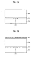
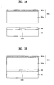
- FIGS. 2A to 2D A method for manufacturing a plasma display panel in accordance with the first embodiment will be described with reference to FIGS. 2A to 2D.
- a barrier rib material 250 is prepared, and is provided on a lower glass 210, on which address electrodes 230 and a dielectric 240 are sequentially provided.
- the barrier rib material 250 is manufactured in a green sheet type and laminated on the lower glass 210, or is manufactured in a paste type and formed on the lower glass 210 by printing or coating.
- the barrier rib material 250 is obtained by mixing a mixture, obtained by mixing several tens of % of an oxide in a powdery state, such as Al 2 O 3 , for improving reflection property and controlling permittivity with PbO or non-PbO glass powder, with an organic solvent.
- a black top material 255 is formed on the barrier rib material 250.
- the black top material 255 has a dry film resist (DFR) function.
- DFR dry film resist
- the black top material 255 is, in this embodiment, manufactured in a green sheet type and laminated on the barrier rib material 250. It may alternatively be manufactured in a paste type and formed on the barrier rib material 250 by printing or coating.
- a black top material having photosensitivity is manufactured in a green sheet type.
- inorganic powder, a black or white pigment, a solvent, a dispersant, a photopolymerization binder, a reactive diluent, and an additive are mixed.
- the inorganic powder have particle sizes of 0.01 ⁇ 100 ⁇ m.
- the photopolymerization binder is selected from the group consisting of unsaturated polyester, acryl, epoxy, and polyethylene, which have an excellent ability to form a film and a high flexibility and facilitate polymerization.
- a polymeric dispersant or an oligomer dispersant in this embodiment, is used as the dispersant.
- the reactive diluent is selected from the group consisting of monomers and acrylates, which have a low viscosity and a medium boiling point.
- a lubricant or a plasticizer in this embodiment, is used as the additive.
- a defoamer is used as the additive.
- the solvent is one selected from the group consisting of aliphatic solvents including alcohols, kitons, esters, ethers, and nucleic acids, and aromatic solvents including toluene and xylene.
- aliphatic solvents including alcohols, kitons, esters, ethers, and nucleic acids
- aromatic solvents including toluene and xylene.
- the obtained solution in which the particles of the inorganic powder are dispersed, is filtrated, and is defoamed, thus being in a stabilized state. Then, the stabilized solution is uniformly applied to the base film, and is dried, and a protection film is attached thereto. Thereby, the manufacture of the black top material is completed.
- barrier rib material 250 and the black top material 255 are treated, thus forming barrier ribs 270 and black tops 280.
- the barrier rib material 250 and the black top material 255 are exposed to light, and are developed.
- a mask 290 is aligned on the upper surface of the black top material 255.
- the mask 290 has light shielding portions 290a and light transmitting portions 290b, which are alternately formed at the same interval.
- the light transmitting portions 290b transmit light so that the light is irradiated onto the barrier rib material 250 under the light transmitting portions 290b and hardens the barrier rib material 250, and the light shielding portions 290a shield light so that the light is not irradiated onto the barrier rib material 250 under the light shielding portions 290a.
- the barrier ribs 270 and the black tops 280 are formed by developing the barrier rib material 250 and the black top material 255.
- the above exposure and development is achieved by sanding, etching, or a photosensitive method, thus removing the barrier rib material 250 and the black top material 255 under the light shielding portions 290a.
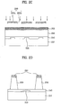
- FIGS. 3A to 3D A method for manufacturing the plasma display panel in accordance with the second embodiment will now be described with reference to FIGS. 3A to 3D.
- a multi-layer green sheet 350 is prepared.
- the multi-layer green sheet 350 includes a barrier rib green sheet 350a, and a black top green sheet 350b having photosensitivity. That is, in the second embodiment, the barrier rib material and the black top material of the first embodiment are combined into a single green sheet, and the green sheet is formed on a lower plate of the plasma display panel. Accordingly, the multi-layer green sheet 350 of the second embodiment includes components of the barrier rib material and the black top material of the first embodiment.
- the multi-layer green sheet 350 is provided on a lower glass 310, on which address electrodes 330 and a dielectric 340 are sequentially provided.
- the multi-layer green sheet 350 is laminated on the lower glass 310.
- the multi-layer green sheet 350 is exposed to the light, and is developed, thus forming barrier ribs.
- a mask 390 is aligned on the upper surface of the multi-layer green sheet 350.
- the mask 390 has light shielding portions 390a and light transmitting portions 390b, which are alternately formed at the same interval.
- the light transmitting portions 390b transmit light so that the light is irradiated onto the barrier rib green sheet 350a under the light transmitting portions 390b and hardens the barrier rib green sheet 350a, and the light shielding portions 390a shield light so that the light is not irradiated onto the barrier rib green sheet 350a under the light shielding portions 290a.
- barrier ribs 370 and black tops 380 are formed by developing the multi-layer green sheet 350.
- the above exposure and development is achieved by sanding, etching, or a photosensitive method, thus removing the multi-layer green sheet 350 under the light shielding portions 390a.
- the black top material and the DFR layer are simultaneously formed, thus reducing production costs of the plasma display panel and shortening the manufacturing process of the plasma display panel.
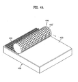
- FIGS. 4A and 4B A method for manufacturing a plasma display panel in accordance with the third embodiment will be described with reference to FIGS. 4A and 4B.
- a barrier rib material 450 is applied to a lower plate 400, on which address electrodes and a dielectric are sequentially provided.
- the barrier rib material 340 is manufactured in a paste type and coated on the lower plate 400. It may alternatively be manufactured in a green sheet and laminated on the lower plate 400.
- Black tops are formed on the barrier rib material 450. The formation of the black tops is performed by an offset or a rolling method. That is, as shown in FIG.
- a black top material 455' on the surface of the blanket roll or the roller 490 is transcribed onto the surface of the barrier rib material 450, and is produced into the black tops 455, as shown in FIG. 4B, by a baking process.
- the barrier rib material 450 is exposed to light using the black tops 455 as a mask, and is developed. That is, since the black tops 455 are obtained by patterning, when ultraviolet light is irradiated onto the lower plate 40, the barrier rib material 450 is selectively exposed to the ultraviolet radiation, and is developed, thus forming barrier ribs.
- the above development is performed by a sanding or an etching method.
- the black tops are formed, and the barrier rib material is exposed to light using the black tops as a mask without using a separate mask, thus simplifying a process for manufacturing the plasma display panel and reducing production costs of the plasma display panel.
- barrier ribs 550 are formed on a lower plate 500, on which address electrodes and a dielectric are provided.
- the barrier ribs 550 are formed by a conventional method, such as a screen printing method, a sanding method, or a photosensitive method.
- black tops 555 are formed on the barrier ribs 550 by an offset method. That is, when a blanket roll 590 is rolled on the barrier ribs 550 formed on the lower plate 500, a black top material 555' on the surface of the blanket roll 590 is transcribed onto the surfaces of the barrier ribs 550, and is produced into the black tops 555 by a baking process.
- a black top material is transferred to a blanket formed on the surface of a blanket roll.
- the black top material is stacked on a master mold and the blanket is rolled on the master mold, the black top material is transferred to the blanket.
- the black top material 555' is transcribed from the blanket roll 590 to the surfaces of the barrier ribs 550, thus forming the black tops 555.
- the method of the fourth embodiment differs from the method of the third embodiment in that the formation of the barrier ribs is completed and then the black top material is formed on the barrier ribs. Since the black top material is formed on the barrier ribs by the offset method, in this particular embodiment the black top material transferred to the blanket has the same pattern of the barrier ribs. In order to prevent the pattern of the barrier ribs and the pattern of the black top material from being deviated from each other, the black top material has a narrower line width than that of the barrier ribs: however, this is not essential to the invention in its broadest aspect.
- barrier ribs 650 are formed on a lower plate 600, on which address electrodes and a dielectric are provided.
- the barrier ribs 650 are formed by a conventional method, such as a screen printing method, a sanding method, or a photosensitive method.
- a black top material 655' on the surface of the roller 690 is transcribed onto the surfaces of the barrier ribs 650, thus forming black tops 655.
- the rolling method comprises a step of transferring the black top material to the roller and a step of transcribing the black top material to the barrier ribs by rolling the roller on the barrier ribs.
- the black top material is transferred to the whole surface of the roller, and then is partially transcribed onto the barrier ribs. Accordingly, when the black top material is transferred to the roller, it is not necessary to adjust the pattern or the line width of the black top material, differently from the fourth embodiment.
- the present invention provides a method for manufacturing a plasma display panel, which can simplify a process for forming barrier ribs and black tops, and reduce the production costs of the plasma display panel.
- the barrier ribs are made of a white material
- the black tops, which are formed on the barrier ribs reduce the reflectance of external light, thus maximizing the contrast of the plasma display panel.
Applications Claiming Priority (2)
| Application Number | Priority Date | Filing Date | Title |
|---|---|---|---|
| KR1020050060221A KR100698157B1 (ko) | 2005-07-05 | 2005-07-05 | 플라즈마 디스플레이 패널의 격벽 제조 방법 |
| KR1020050082617A KR20070027226A (ko) | 2005-09-06 | 2005-09-06 | 플라즈마 디스플레이 패널의 하부패널 및 블랙탑 형성방법 |
Publications (2)
| Publication Number | Publication Date |
|---|---|
| EP1742244A2 true EP1742244A2 (fr) | 2007-01-10 |
| EP1742244A3 EP1742244A3 (fr) | 2008-04-02 |
Family
ID=37057405
Family Applications (1)
| Application Number | Title | Priority Date | Filing Date |
|---|---|---|---|
| EP06253521A Withdrawn EP1742244A3 (fr) | 2005-07-05 | 2006-07-05 | Procédé de fabrication d'un panneau d'affichage à plasma |
Country Status (3)
| Country | Link |
|---|---|
| US (1) | US20070013307A1 (fr) |
| EP (1) | EP1742244A3 (fr) |
| JP (1) | JP2007019019A (fr) |
Cited By (1)
| Publication number | Priority date | Publication date | Assignee | Title |
|---|---|---|---|---|
| EP1742245A2 (fr) * | 2005-07-08 | 2007-01-10 | LG Electronic Inc. | Feuille verte supérieure noire, panneau d'affichage à plasma et procédé de fabrication de celui-ci |
Citations (3)
| Publication number | Priority date | Publication date | Assignee | Title |
|---|---|---|---|---|
| US5909083A (en) * | 1996-02-16 | 1999-06-01 | Dai Nippon Printing Co., Ltd. | Process for producing plasma display panel |
| JP2004148585A (ja) * | 2002-10-29 | 2004-05-27 | Hitachi Chem Co Ltd | エレメントおよびその利用 |
| US20040248048A1 (en) * | 2003-06-04 | 2004-12-09 | Lg Electronics Inc. | Barrier rib of plasma display panel and forming method thereof |
Family Cites Families (2)
| Publication number | Priority date | Publication date | Assignee | Title |
|---|---|---|---|---|
| JP2716013B2 (ja) * | 1995-08-11 | 1998-02-18 | 日本電気株式会社 | カラープラズマディスプレイパネルおよびその製造方法 |
| US6008582A (en) * | 1997-01-27 | 1999-12-28 | Dai Nippon Printing Co., Ltd. | Plasma display device with auxiliary partition walls, corrugated, tiered and pigmented walls |
-
2006
- 2006-07-05 JP JP2006185324A patent/JP2007019019A/ja not_active Withdrawn
- 2006-07-05 EP EP06253521A patent/EP1742244A3/fr not_active Withdrawn
- 2006-07-05 US US11/480,562 patent/US20070013307A1/en not_active Abandoned
Patent Citations (3)
| Publication number | Priority date | Publication date | Assignee | Title |
|---|---|---|---|---|
| US5909083A (en) * | 1996-02-16 | 1999-06-01 | Dai Nippon Printing Co., Ltd. | Process for producing plasma display panel |
| JP2004148585A (ja) * | 2002-10-29 | 2004-05-27 | Hitachi Chem Co Ltd | エレメントおよびその利用 |
| US20040248048A1 (en) * | 2003-06-04 | 2004-12-09 | Lg Electronics Inc. | Barrier rib of plasma display panel and forming method thereof |
Cited By (2)
| Publication number | Priority date | Publication date | Assignee | Title |
|---|---|---|---|---|
| EP1742245A2 (fr) * | 2005-07-08 | 2007-01-10 | LG Electronic Inc. | Feuille verte supérieure noire, panneau d'affichage à plasma et procédé de fabrication de celui-ci |
| EP1742245A3 (fr) * | 2005-07-08 | 2009-01-21 | LG Electronic Inc. | Feuille verte supérieure noire, panneau d'affichage à plasma et procédé de fabrication de celui-ci |
Also Published As
| Publication number | Publication date |
|---|---|
| EP1742244A3 (fr) | 2008-04-02 |
| US20070013307A1 (en) | 2007-01-18 |
| JP2007019019A (ja) | 2007-01-25 |
Similar Documents
| Publication | Publication Date | Title |
|---|---|---|
| EP1898429A1 (fr) | Composite de pâte pour électrodes, structure de plaque frontale de panneau d'affichage à plasma et procédé de fabrication utilisant le composite | |
| JP2004241379A (ja) | プラズマディスプレイ部材およびプラズマディスプレイ、並びにプラズマディスプレイ部材の製造方法 | |
| US6893803B2 (en) | Barrier rib of plasma display panel and forming method thereof | |
| EP1754722B1 (fr) | Composite à base d'une pâte noire, plaque supérieure d'un panneau d'affichage à plasma et son procédé de préparation | |
| KR100730044B1 (ko) | 격벽용 슬러리, 그린시트 및 플라즈마 디스플레이 패널의격벽 제조방법 | |
| EP1803692B1 (fr) | Feuille verte pour la préparation des nervures d'isolation dans un panneau d'affichage à plasma | |
| EP1627406B1 (fr) | Stratifie non cuit permettant de produire une plaque frontale d'ecran a plasma, et procede de production d'une plaque frontale d'ecran a plasma | |
| EP1742244A2 (fr) | Procédé de fabrication d'un panneau d'affichage à plasma | |
| JP4411940B2 (ja) | 無機材料ペースト、およびプラズマディスプレイ部材ならびにプラズマディスプレイ | |
| JPH09115452A (ja) | プラズマディスプレイパネルの障壁構造 | |
| EP1742245A2 (fr) | Feuille verte supérieure noire, panneau d'affichage à plasma et procédé de fabrication de celui-ci | |
| KR20070108345A (ko) | 전도성 조성물 및 플라즈마 디스플레이의 배면 기판의 제조방법 | |
| US20050215161A1 (en) | Plasma display panel manufacturing method | |
| JP2008159360A (ja) | プラズマディスプレイパネルの製造方法 | |
| JP4013340B2 (ja) | プラズマディスプレイ用部材 | |
| JP2008226516A (ja) | プラズマディスプレイパネルの製造方法およびプラズマディスプレイパネル | |
| KR20050008721A (ko) | 플라즈마 디스플레이 패널의 제조 방법 및 플라즈마디스플레이 패널 | |
| JP2002302648A (ja) | 絶縁膜形成用塗料、及びそれを用いたプラズマディスプレイパネルとその製造方法 | |
| JP4200264B2 (ja) | シート状誘電体材料およびそれを用いたプラズマディスプレイパネルの製造方法 | |
| KR100829252B1 (ko) | 격벽용 시트의 제조방법, 플라즈마 디스플레이 패널의 격벽 제조방법 및 플라즈마 디스플레이 패널 | |
| KR940006293B1 (ko) | 플라즈마 디스플레이 패널 | |
| JP2005209636A (ja) | プラズマディスプレイ部材およびプラズマディスプレイ | |
| KR100898295B1 (ko) | 플라즈마 디스플레이 패널 | |
| KR100698157B1 (ko) | 플라즈마 디스플레이 패널의 격벽 제조 방법 | |
| KR20060086776A (ko) | 플라즈마 디스플레이 패널의 격벽 제조 방법 |
Legal Events
| Date | Code | Title | Description |
|---|---|---|---|
| PUAI | Public reference made under article 153(3) epc to a published international application that has entered the european phase |
Free format text: ORIGINAL CODE: 0009012 |
|
| AK | Designated contracting states |
Kind code of ref document: A2 Designated state(s): AT BE BG CH CY CZ DE DK EE ES FI FR GB GR HU IE IS IT LI LT LU LV MC NL PL PT RO SE SI SK TR |
|
| AX | Request for extension of the european patent |
Extension state: AL BA HR MK YU |
|
| RIN1 | Information on inventor provided before grant (corrected) |
Inventor name: RYU, BYUNG GIL Inventor name: KIM, JE SEOK Inventor name: LEE, HONG CHEOL Inventor name: PARK, DEOK HAI Inventor name: SHIN, DONG OH Inventor name: JEON, WON SEOK Inventor name: PARK, MIN SOO Inventor name: SEO, BYUNG HWA Inventor name: KIM, KYUNG KU404-1006 HANGARAM SILLA APT. Inventor name: PARK, DAE HYUN505-505 KUMBO BESTVILL APT. |
|
| PUAL | Search report despatched |
Free format text: ORIGINAL CODE: 0009013 |
|
| AK | Designated contracting states |
Kind code of ref document: A3 Designated state(s): AT BE BG CH CY CZ DE DK EE ES FI FR GB GR HU IE IS IT LI LT LU LV MC NL PL PT RO SE SI SK TR |
|
| AX | Request for extension of the european patent |
Extension state: AL BA HR MK YU |
|
| 17P | Request for examination filed |
Effective date: 20080527 |
|
| 17Q | First examination report despatched |
Effective date: 20080715 |
|
| AKX | Designation fees paid |
Designated state(s): DE FR GB NL |
|
| STAA | Information on the status of an ep patent application or granted ep patent |
Free format text: STATUS: THE APPLICATION IS DEEMED TO BE WITHDRAWN |
|
| 18D | Application deemed to be withdrawn |
Effective date: 20081126 |