EP1741315B1 - Lichtemittierende bauelemente mit mehreren verkapselungsschichten, wobei mindestens eine der verkapselungsschichten nanopartikel enthält, und herstellungsverfahren dafür - Google Patents
Lichtemittierende bauelemente mit mehreren verkapselungsschichten, wobei mindestens eine der verkapselungsschichten nanopartikel enthält, und herstellungsverfahren dafür Download PDFInfo
- Publication number
- EP1741315B1 EP1741315B1 EP05734066A EP05734066A EP1741315B1 EP 1741315 B1 EP1741315 B1 EP 1741315B1 EP 05734066 A EP05734066 A EP 05734066A EP 05734066 A EP05734066 A EP 05734066A EP 1741315 B1 EP1741315 B1 EP 1741315B1
- Authority
- EP
- European Patent Office
- Prior art keywords
- encapsulation layer
- light
- nanoparticles
- matrix material
- emitting device
- Prior art date
- Legal status (The legal status is an assumption and is not a legal conclusion. Google has not performed a legal analysis and makes no representation as to the accuracy of the status listed.)
- Active
Links
- 238000005538 encapsulation Methods 0.000 title claims abstract description 125
- 239000002105 nanoparticle Substances 0.000 title claims abstract description 46
- 238000000034 method Methods 0.000 title claims description 25
- 239000011159 matrix material Substances 0.000 claims abstract description 40
- 230000000704 physical effect Effects 0.000 claims abstract description 23
- GWEVSGVZZGPLCZ-UHFFFAOYSA-N Titan oxide Chemical compound O=[Ti]=O GWEVSGVZZGPLCZ-UHFFFAOYSA-N 0.000 claims description 46
- 229920001296 polysiloxane Polymers 0.000 claims description 39
- 230000003287 optical effect Effects 0.000 claims description 32
- 239000011521 glass Substances 0.000 claims description 19
- 239000002245 particle Substances 0.000 claims description 18
- 229920000642 polymer Polymers 0.000 claims description 18
- HBMJWWWQQXIZIP-UHFFFAOYSA-N silicon carbide Chemical compound [Si+]#[C-] HBMJWWWQQXIZIP-UHFFFAOYSA-N 0.000 claims description 17
- 229910010271 silicon carbide Inorganic materials 0.000 claims description 17
- 238000006243 chemical reaction Methods 0.000 claims description 16
- 239000003822 epoxy resin Substances 0.000 claims description 16
- 239000000945 filler Substances 0.000 claims description 16
- 239000000463 material Substances 0.000 claims description 16
- 229920000647 polyepoxide Polymers 0.000 claims description 16
- 238000005299 abrasion Methods 0.000 claims description 15
- 239000004964 aerogel Substances 0.000 claims description 15
- 150000001875 compounds Chemical class 0.000 claims description 15
- 229910003460 diamond Inorganic materials 0.000 claims description 15
- 239000010432 diamond Substances 0.000 claims description 15
- 239000000499 gel Substances 0.000 claims description 15
- 238000004519 manufacturing process Methods 0.000 description 12
- 239000000758 substrate Substances 0.000 description 9
- 239000004593 Epoxy Substances 0.000 description 8
- 238000000605 extraction Methods 0.000 description 8
- 238000007789 sealing Methods 0.000 description 8
- 238000004806 packaging method and process Methods 0.000 description 7
- 238000010586 diagram Methods 0.000 description 6
- 238000005266 casting Methods 0.000 description 5
- 239000000654 additive Substances 0.000 description 4
- OAICVXFJPJFONN-UHFFFAOYSA-N Phosphorus Chemical compound [P] OAICVXFJPJFONN-UHFFFAOYSA-N 0.000 description 3
- 239000004020 conductor Substances 0.000 description 3
- 238000004377 microelectronic Methods 0.000 description 3
- 150000004767 nitrides Chemical class 0.000 description 3
- 239000004033 plastic Substances 0.000 description 3
- 239000000126 substance Substances 0.000 description 3
- 230000004907 flux Effects 0.000 description 2
- 238000012986 modification Methods 0.000 description 2
- 229920002379 silicone rubber Polymers 0.000 description 2
- VLCQZHSMCYCDJL-UHFFFAOYSA-N tribenuron methyl Chemical compound COC(=O)C1=CC=CC=C1S(=O)(=O)NC(=O)N(C)C1=NC(C)=NC(OC)=N1 VLCQZHSMCYCDJL-UHFFFAOYSA-N 0.000 description 2
- NCGICGYLBXGBGN-UHFFFAOYSA-N 3-morpholin-4-yl-1-oxa-3-azonia-2-azanidacyclopent-3-en-5-imine;hydrochloride Chemical compound Cl.[N-]1OC(=N)C=[N+]1N1CCOCC1 NCGICGYLBXGBGN-UHFFFAOYSA-N 0.000 description 1
- JBRZTFJDHDCESZ-UHFFFAOYSA-N AsGa Chemical compound [As]#[Ga] JBRZTFJDHDCESZ-UHFFFAOYSA-N 0.000 description 1
- 229910005540 GaP Inorganic materials 0.000 description 1
- 229910001218 Gallium arsenide Inorganic materials 0.000 description 1
- 229920001807 Urea-formaldehyde Polymers 0.000 description 1
- 230000000996 additive effect Effects 0.000 description 1
- 229910045601 alloy Inorganic materials 0.000 description 1
- 239000000956 alloy Substances 0.000 description 1
- 239000003795 chemical substances by application Substances 0.000 description 1
- 230000000295 complement effect Effects 0.000 description 1
- 238000011161 development Methods 0.000 description 1
- 230000018109 developmental process Effects 0.000 description 1
- HZXMRANICFIONG-UHFFFAOYSA-N gallium phosphide Chemical compound [Ga]#P HZXMRANICFIONG-UHFFFAOYSA-N 0.000 description 1
- TWNQGVIAIRXVLR-UHFFFAOYSA-N oxo(oxoalumanyloxy)alumane Chemical compound O=[Al]O[Al]=O TWNQGVIAIRXVLR-UHFFFAOYSA-N 0.000 description 1
- 229910052594 sapphire Inorganic materials 0.000 description 1
- 239000010980 sapphire Substances 0.000 description 1
- 229920002050 silicone resin Polymers 0.000 description 1
- 239000004945 silicone rubber Substances 0.000 description 1
- 239000007787 solid Substances 0.000 description 1
- 238000001429 visible spectrum Methods 0.000 description 1
Images
Classifications
-
- H—ELECTRICITY
- H01—ELECTRIC ELEMENTS
- H01L—SEMICONDUCTOR DEVICES NOT COVERED BY CLASS H10
- H01L33/00—Semiconductor devices having potential barriers specially adapted for light emission; Processes or apparatus specially adapted for the manufacture or treatment thereof or of parts thereof; Details thereof
- H01L33/48—Semiconductor devices having potential barriers specially adapted for light emission; Processes or apparatus specially adapted for the manufacture or treatment thereof or of parts thereof; Details thereof characterised by the semiconductor body packages
- H01L33/52—Encapsulations
- H01L33/54—Encapsulations having a particular shape
-
- H—ELECTRICITY
- H05—ELECTRIC TECHNIQUES NOT OTHERWISE PROVIDED FOR
- H05B—ELECTRIC HEATING; ELECTRIC LIGHT SOURCES NOT OTHERWISE PROVIDED FOR; CIRCUIT ARRANGEMENTS FOR ELECTRIC LIGHT SOURCES, IN GENERAL
- H05B33/00—Electroluminescent light sources
- H05B33/02—Details
- H05B33/04—Sealing arrangements, e.g. against humidity
-
- H—ELECTRICITY
- H01—ELECTRIC ELEMENTS
- H01L—SEMICONDUCTOR DEVICES NOT COVERED BY CLASS H10
- H01L33/00—Semiconductor devices having potential barriers specially adapted for light emission; Processes or apparatus specially adapted for the manufacture or treatment thereof or of parts thereof; Details thereof
- H01L33/48—Semiconductor devices having potential barriers specially adapted for light emission; Processes or apparatus specially adapted for the manufacture or treatment thereof or of parts thereof; Details thereof characterised by the semiconductor body packages
- H01L33/52—Encapsulations
- H01L33/56—Materials, e.g. epoxy or silicone resin
Definitions
- the present invention relates generally to microelectronic devices and fabrication methods therefor, and, more particularly, to light-emitting devices and fabrication methods therefor.
- LEDs Light-emitting diodes
- a light-emitting diode generally includes an active region on a microelectronic substrate.
- the microelectronic substrate may comprise, for example, gallium arsenide, gallium phosphide, alloys thereof, silicon carbide, and/or sapphire.
- Standard LED packaging typically comprises an epoxy-based encapsulation layer to both protect the active device from the elements and to enhance the optical output of the LED device.
- an epoxy-based encapsulation layer may optically degrade when used with relatively short wavelength (e . g ., 525 nm), high flux LEDs.
- Document US 2003/122 482 discloses a light-emitting element containing a first and second sealing member, wherein the first sealing member is covering the light-emitting element and the second sealing member is covering the first sealing member.
- the said sealing members are made of epoxy resin, silicone resin, silicone rubber, silicone elastomer, urea resin or glass.
- As light-diffusing agent e.g. TiO 2 is added to the sealing member.
- organic fluorescent substances can be added or phosphors.
- the additives are added as micron-size particles.
- a plurality of sealing members into which silicone members contain different kinds of additives may be also prepared.
- the second sealing members can also contain additives.
- a light-emitting device includes an active region that is configured to emit light responsive to a voltage applied thereto.
- a first encapsulation layer at least partially encapsulates the active region and includes a matrix material and nanoparticles, which modify at least one physical property of the first encapsulation layer.
- a second encapsulation layer at least partially encapsulates the first encapsulation layer.
- the matrix material comprises silicone, a silicone compound, an optical gel, epoxy resin, glass, sol-gel, aerogel, and/or an optically stable polymer.
- the first encapsulation layer is substantially transparent.
- the nanoparticles comprise TiO 2 , diamond, silicon carbide, scattering particles, fillers, phosphors, and/or light conversion materials.
- the at least one physical property comprises index of refraction, thermal conductivity, mechanical strength, abrasion resistance, and/or optical stability.
- the matrix material is a first matrix material
- the nanoparticles are first nanoparticles.
- the second encapsulation layer comprises a second matrix material and second nanoparticles that modify at least one physical property of the second encapsulation layer.
- the second matrix material comprises silicone, a silicone compound, an optical gel, epoxy resin, glass, sol-gel, aerogel, and/or an optically stable polymer.
- the second encapsulation layer is substantially transparent.
- the second nanoparticles comprise TiO 2 , diamond, silicon carbide, scattering particles, fillers, phosphors, and/or light conversion materials.
- the at least one physical property of the second encapsulation layer comprises index of refraction, thermal conductivity, mechanical strength, abrasion resistance, and/or optical stability.
- an outer surface of the first encapsulation layer, opposite the active region may be shaped so that light rays from the active region are not incident on the first encapsulation layer at an angle that is greater than a critical angle.
- the present invention may also be embodied as fabrication methods of forming light-emitting devices.
- first, second, etc. may be used herein to describe various elements, components, regions, layers and/or sections, these elements, components, regions, layers and/or sections should not be limited by these terms. These terms are only used to distinguish one element, component, region, layer or section from another region, layer or section. Thus, a first region, layer or section discussed below could be termed a second region, layer or section, and, similarly, a second without departing from the teachings of the present invention.
- Embodiments of the present invention will now be described, generally, with reference to GaN-based light-emitting diodes (LEDs) on SiC-based or sapphire (Al 2 O 3 )-based substrates.
- LEDs light-emitting diodes
- Al 2 O 3 sapphire
- the present invention is not limited to such structures.
- Examples of light-emitting devices that may be used in embodiments of the present invention include, but are not limited to, LEDs and/or laser diodes, such as devices manufactured and sold by Cree, Inc. of Durham, North Carolina.
- the present invention may be suitable for use with LEDs and/or lasers as described in United States Patent Nos.
- the LEDs and/or lasers may be configured to operate in a "flip-chip" configuration such that light emission occurs through the substrate.
- the substrate may be patterned so as to enhance light output of the devices as is described, for example, in United States Patent Application Serial No. 10/057,821, filed January 25, 2002 entitled "LIGHT EMITTING DIODES INCLUDING SUBSTRATE MODIFICATIONS FOR LIGHT EXTRACTION AND MANUFACTURING METHODS THEREFOR".
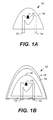
- FIGS. 1A 1B are cross-sectional diagrams that illustrate light-emitting devices and fabrication methods therefor, in accordance with some embodiments of the present invention.
- a light-emitting device 10 in accordance with some embodiments of the present invention, includes an LED, which includes an anode terminal 12, an active region 13, such as a diode region, and a cathode terminal 14, which are electrically coupled to one another.
- the active region 13 is configured to emit light responsive to a voltage applied thereto via, for example, the anode and cathode terminals 12 and 14.
- the light-emitting device 10 further includes a first encapsulation layer 16, which includes, for example, a matrix material and nanoparticles that modify at least one physical property, such as, for example, index of refraction, thermal conductivity, mechanical strength, abrasion resistance, and/or optical stability of the first encapsulation layer 16.
- the first encapsulation layer 16 at least partially encapsulates the active region in accordance with some embodiments of the present invention and may be substantially transparent.
- the matrix material may comprise silicone, a silicone compound, an optical gel, epoxy resin, glass, sol-gel, aerogel, and/or an optically stable polymer.
- the silicone gel is generally optically stable when exposed to relatively high flux, short wavelength light ( e .
- the nanoparticles in the first encapsulation layer 16 may comprise TiO 2 , diamond, silicon carbide, scattering particles, fillers, phosphors, and/or light conversion materials.
- the first encapsulation layer 16 may comprise a silicone gel having TiO 2 nanoparticles contained therein.
- the TiO 2 nanoparticles contained in the silicone gel may increase the index of refraction of the first encapsulation layer 16 to allow the index of refraction of the first encapsulation layer 16 to more closely match the index of refraction of the active region 13 thereby improving light extraction from the active region 13.
- n 1 sin ⁇ 1 n 2 sin ⁇ 2 , where n 1 is the index of refraction for medium 1 and n 2 is the index of refraction for medium 2.
- ⁇ 1critical sin -1 (n 2 /n 1 )
- Light that is incident at an angle greater than the critical angle does not pass through to medium 2, but is instead reflected back into medium 1. This reflection is commonly called total internal reflection.
- an outer surface of the first encapsulation layer 16, opposite the active region 13, may be shaped so that light rays from the active region 13 are not incident on the first encapsulation layer 16 at an angle that is greater than the critical angle, in accordance with some embodiments of the present invention.
- the first encapsulation layer 16 is at least partially encapsulated with a second encapsulation layer 18, which may comprise a second matrix material and second nanoparticles that modify at least one physical property, such as, for example, index of refraction, thermal conductivity, mechanical strength, abrasion resistance, and/or optical stability of the second encapsulation layer 18.
- the second encapsulation layer 18 and may be substantially transparent.
- the second matrix material may comprise silicone, a silicone compound, an optical gel, epoxy resin, glass, sol-gel, aerogel, and/or an optically stable polymer.
- the second nanoparticles may comprise TiO 2 , diamond, silicon carbide, scattering particles, fillers, phosphors, and/or light conversion materials.
- the second encapsulation layer 18 may include epoxy, plastic, and/or glass to add rigidity to the packaging of the light-emitting device 10.
- a third encapsulation layer 19, which may be substantially transparent, may be used to at least partially encapsulate the second encapsulation layer 18 in accordance with some embodiments of the present invention.
- the third encapsulation layer 19 may include a thermally conductive material.
- the first, second, and third encapsulation layers 16, 18, and 19 may be formed using a casting process.
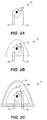
- FIGS. 2A - 2C are cross-sectional diagrams that illustrate light-emitting devices and fabrication methods therefor, in accordance with further embodiments of the present invention.
- a light-emitting device 20 in accordance with some embodiments of the present invention, includes an LED, which includes an anode terminal 22, an active region 23, such as a diode region, and a cathode terminal 24, which are electrically coupled to one another.
- the active region 23 is configured to emit light responsive to a voltage applied thereto via, for example, the anode and cathode terminals 22 and 24.
- the light-emitting device 20 further includes a first encapsulation layer 26, which includes, for example, a matrix material and nanoparticles that modify at least one physical property, such as, for example, index of refraction, thermal conductivity, mechanical strength, abrasion resistance, and/or optical stability of the first encapsulation layer 26.
- the first encapsulation layer 26 at least partially encapsulates the active region in accordance with some embodiments of the present invention and may be substantially transparent.
- the matrix material may comprise silicone, a silicone compound, an optical gel, epoxy resin, glass, sol-gel, aerogel, and/or an optically stable polymer.
- the nanoparticles in the first encapsulation layer 26 may comprise TiO 2 , diamond, silicon carbide, scattering particles, fillers, phosphors, and/or light conversion materials.
- the first encapsulation layer 26 may comprise silicone gel, epoxy, and/or a polymer having TiO 2 nanoparticles contained therein.
- the TiO 2 nanoparticles contained in the matrix material may increase the index of refraction of the first encapsulation layer 26 to allow the index of refraction of the first encapsulation layer 26 to more closely match the index of refraction of the active region 23 thereby improving light extraction from the active region 23.
- an outer surface of the first encapsulation layer 26, opposite the active region 23, may be shaped so that light rays from the active region 23 are not incident on the first encapsulation layer 26 at an angle that is greater than the critical angle, in accordance with some embodiments of the present invention.
- the first encapsulation layer 26 may further include phosphor particles, to fabricate, for example, a white LED lamp, in accordance with some embodiments of the present invention.
- the first encapsulation layer 26 may be formed using a casting or dispensing process.
- the light-emitting device 20 further comprises a second encapsulation layer 27 that at least partially encapsulates the first encapsulation layer 26 and may be substantially transparent.
- the second encapsulation layer 27 may comprise a second matrix material and second nanoparticles that modify at least one physical property, such as, for example, index of refraction, thermal conductivity, mechanical strength, abrasion resistance, and/or optical stability of the second encapsulation layer 27.
- the second matrix material may comprise silicone, a silicone compound, an optical gel, epoxy resin, glass, sol-gel, aerogel, and/or an optically stable polymer.
- the second nanoparticles may comprise TiO 2 , diamond, silicon carbide, scattering particles, fillers, phosphors, and/or light conversion materials.
- the second encapsulation layer 27 may comprise silicone gel.
- the second encapsulation layer 27 is at least partially encapsulated with a third encapsulation layer 28, which may be substantially transparent and may comprise a third matrix material and third nanoparticles that modify at least one physical property, such as, for example, index of refraction, thermal conductivity, mechanical strength, abrasion resistance, and/or optical stability of the third encapsulation layer 28.
- the third matrix material may comprise silicone, a silicone compound, an optical gel, epoxy resin, glass, sol-gel, aerogel, and/or an optically stable polymer.
- the third nanoparticles may comprise TiO 2 , diamond, silicon carbide, scattering particles, fillers, phosphors, and/or light conversion materials.
- the third encapsulation layer 28 may include epoxy, plastic, and/or glass to add rigidity to the packaging of the light-emitting device 20.
- a fourth encapsulation layer 29 may be used to at least partially encapsulate the third encapsulation layer 28 in accordance with some embodiments of the present invention.
- the fourth encapsulation layer 29 may include a thermally conductive material and may be substantially transparent.
- the second, third, and fourth encapsulation layers 27, 28, and 29 may be formed using a casting process.
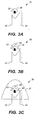
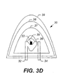
- FIGS. 3A - 3D are cross-sectional diagrams that illustrate light-emitting devices and fabrication methods therefor, in accordance with some other embodiments of the present invention.
- a light-emitting device 30 in accordance with some embodiments of the present invention, includes an LED, which includes an anode terminal 32, an active region 33, such as a diode region, and a cathode terminal 34, which are electrically coupled to one another.
- the active region 33 is configured to emit light responsive to a voltage applied thereto via, for example, the anode and cathode terminals 32 and 34.
- the light-emitting device 30 further includes a first encapsulation layer 35, which includes, for example, a matrix material and nanoparticles that modify at least one physical property, such as, for example, index of refraction, thermal conductivity, mechanical strength, abrasion resistance, and/or optical stability of the first encapsulation layer 35.
- the first encapsulation layer 35 at least partially encapsulates the active region and may be substantially transparent in accordance with some embodiments of the present invention.
- the matrix material may comprise silicone, a silicone compound, an optical gel, epoxy resin, glass, sol-gel, aerogel, and/or an optically stable polymer.
- the nanoparticles in the first encapsulation layer 35 may comprise TiO 2 , diamond, silicon carbide, scattering particles, fillers, phosphors, and/or light conversion materials.
- the first encapsulation layer 35 may comprise silicone gel, epoxy, and/or a polymer having TiO 2 nanoparticles contained therein.
- the TiO 2 nanoparticles contained in the matrix material may increase the index of refraction of the first encapsulation layer 36 to allow the index of refraction of the first encapsulation layer 35 to more closely match the index of refraction of the active region 35 thereby improving light extraction from the active region 33.
- an outer surface of the first encapsulation layer 35, opposite the active region 33, may be shaped so that light rays from the active region 33 are not incident on the first encapsulation layer 35 at an angle that is greater than the critical angle, in accordance with some embodiments of the present invention.
- the light-emitting device 30 further comprises a second encapsulation layer 36 that at least partially encapsulates the first encapsulation layer 35 and may be substantially transparent.
- the second encapsulation layer 36 may comprise a second matrix material and second nanoparticles that modify at least one physical property, such as, for example, index of refraction, thermal conductivity, mechanical strength, abrasion resistance, and/or optical stability of the second encapsulation layer 36.
- the second matrix material may comprise silicone, a silicone compound, an optical gel, epoxy resin, glass, sol-gel, aerogel, and/or an optically stable polymer.
- the second nanoparticles may comprise TiO 2 , diamond, silicon carbide, scattering particles, fillers, phosphors, and/or light conversion materials.
- the second encapsulation layer 36 may comprise silicone gel, epoxy, and/or a polymer having phosphor particles contained therein to fabricate, for example, a white LED lamp, in accordance with some embodiments of the present invention.
- the second encapsulation layer 36 may further include TiO 2 nanoparticles in accordance with some embodiments of the present invention.
- the first and second encapsulation layers 35 and 36 may be formed using a casting or dispensing process.
- the light-emitting device 30 further comprises a third encapsulation layer 37, that at least partially encapsulates the second encapsulation layer 36 and may be substantially transparent.
- the third encapsulation layer 37 may comprise a third matrix material and third nanoparticles that modify at least one physical property, such as, for example, index of refraction, thermal conductivity, mechanical strength, abrasion resistance, and/or optical stability of the third encapsulation layer 37.
- the third matrix material may comprise silicone, a silicone compound, an optical gel, epoxy resin, glass, sol-gel, aerogel, and/or an optically stable polymer.
- the third nanoparticles may comprise TiO 2 , diamond, silicon carbide, scattering particles, fillers, phosphors, and/or light conversion materials.
- the third encapsulation layer 37 may comprise silicone gel.
- the third encapsulation layer 37 is at least partially encapsulated with a fourth encapsulation layer 38; which may be substantially transparent and may comprise a fourth matrix material and fourth nanoparticles that modify at least one physical property, such as, for example, index of refraction, thermal conductivity, mechanical strength, abrasion resistance, and/or optical stability of the fourth encapsulation layer 38.
- the fourth matrix material may comprise silicone, a silicone compound, an optical gel, epoxy resin, glass, sol-gel, aerogel, and/or an optically stable polymer.
- the fourth nanoparticles may comprise TiO 2 , diamond, silicon carbide, scattering particles, fillers, phosphors, and/or light conversion materials.
- the fourth encapsulation layer 38 may include epoxy, plastic, and/or glass to add rigidity to the packaging of the light-emitting device 30.
- a fifth encapsulation layer 39 may be used to at least partially encapsulate the fourth encapsulation layer 38 in accordance with some embodiments of the present invention.
- the fifth encapsulation layer 39 may include a thermally conductive material and may be substantially transparent.
- the third, fourth, and fifth encapsulation layers 37, 38, and 39 may be formed using a casting process.
- embodiments of the invention may comprise a sequence of multiple (two or more) encapsulation layers, each either fully or partially encapsulating the previous layers or light-emitting device.
- Each encapsulation layer may comprise one of a variety of matrix, nanoparticle, additive/filler materials as described above, and each layer may serve a specific complimentary function to improve the performance of the resulting package. It is generally desirable that the encapsulation layers do not substantially absorb light from the light-emitting device.
- the interface between the encapsulation layers may be designed to enhance the optical and/or chemical properties. Compatibility of chemical and other physical properties, such as chemical reactions, adhesion, thermal expansion, etc. may place constraints upon the geometry and/or the configuration of the interface between various encapsulation layers.
Landscapes
- Engineering & Computer Science (AREA)
- Microelectronics & Electronic Packaging (AREA)
- Manufacturing & Machinery (AREA)
- Computer Hardware Design (AREA)
- Power Engineering (AREA)
- Led Device Packages (AREA)
- Electroluminescent Light Sources (AREA)
- Luminescent Compositions (AREA)
Claims (22)
- Lichtemittierende Vorrichtung, die aufweist:einen aktiven Bereich (13), der so ausgestaltet ist, daß er Licht in Reaktion auf eine daran angelegte Spannung emittiert,eine erste Kapselungsschicht (16), die den aktiven Bereich wenigstens teilweise kapselt, wobei die erste Kapselungsschicht ein Matrixmaterial und Nanopartikel, die wenigstens eine physikalische Eigenschaft der ersten Kapselungsschicht modifizieren, beinhaltet, undeine zweite Kapselungsschicht (18), die die erste Kapselungsschicht wenigstens teilweise kapselt.
- Lichtemittierende Vorrichtung nach Anspruch 1, wobei das Matrixmaterial Silikon, eine Silikonverbindung, ein optisches Gel, Epoxidharz, Glas, Sol-Gel, Aerogel und/oder ein optisch stabiles Polymer beinhaltet.
- Lichtemittierende Vorrichtung nach Anspruch 1 oder Anspruch 2, wobei die erste Kapselungsschicht im wesentlichen transparent ist.
- Lichtemittierende Vorrichtung nach einem der vorangegangenen Ansprüche, wobei die Nanopartikel TiO2, Diamant, Siliciumcarbid, Streuungspartikel, Füllmittel, Leuchtstoffe und/oder Lichtumwandlungsmaterialien beinhalten.
- Lichtemittierende Vorrichtung nach einem der vorangegangenen Ansprüche, wobei die physikalische Eigenschaft den Brechungsindex, die Wärmeleitfähigkeit, die mechanische Festigkeit, die Abriebbeständigkeit und/oder die optische Stabilität beinhaltet.
- Lichtemittierende Vorrichtung nach einem der vorangegangenen Ansprüche, wobei das Matrixmaterial der ersten Kapselungsschicht (16) ein erstes Matrixmaterial ist und die Nanopartikel darin erste Nanopartikel sind und wobei die zweite Kapselungsschicht (18) ein zweites Matrixmaterial und zweite Nanopartikel, die wenigstens eine physikalische Eigenschaft der zweiten Kapselungsschicht modifizieren, beinhaltet.
- Lichtemittierende Vorrichtung nach Anspruch 6, wobei das zweite Matrixmaterial Silikon, eine Silikonverbindung, ein optisches Gel, Epoxidharz, Glas, Sol-Gel, Aerogel und/oder ein optisch stabiles Polymer beinhaltet.
- Lichtemittierende Vorrichtung nach Anspruch 6 oder Anspruch 7, wobei die zweite Kapselungsschicht im wesentlichen transparent ist.
- Lichtemittierende Vorrichtung nach einem der Ansprüche 6 bis 8, wobei die zweiten Nanopartikel TiO2, Diamant, Siliciumcarbid, Streuungspartikel, Füllmittel, Leuchtstoffe und/oder Lichtumwandlungsmaterialien beinhalten.
- Lichtemittierende Vorrichtung nach einem der Ansprüche 6 bis 9, wobei die physikalische Eigenschaft der zweiten Kapselungsschicht (18) den Brechungsindex, die Wärmeleitfähigkeit, die mechanische Festigkeit, die Abriebbeständigkeit und/oder die optische Stabilität beinhaltet.
- Lichtemittierende Vorrichtung nach einem der vorangegangenen Ansprüche, wobei eine äußere Oberfläche der ersten Kapselungsschicht (16) gegenüber dem aktiven Bereich (13) so geformt ist, daß Lichtstrahlen von dem aktiven Bereich nicht unter einem Winkel, der größer ist als ein kritischer Winkel, auf die erste Kapselungsschicht einfallen.
- Verfahren zum Bilden einer lichtemittierenden Vorrichtung (10), welches umfaßt:Bilden eines aktiven Bereichs (13), der so ausgestaltet ist, daß er Licht in Reaktion auf eine daran angelegte Spannung emittiert,Bilden einer ersten Kapselungsschicht (16), die den aktiven Bereich wenigstens teilweise kapselt, wobei die erste Kapselungsschicht ein Matrixmaterial und Nanopartikel, die wenigstens eine physikalische Eigenschaft der ersten Kapselungsschicht modifizieren, beinhaltet, undBilden einer zweiten Kapselungsschicht (18), die die erste Kapselungsschicht wenigstens teilweise kapselt.
- Verfahren nach Anspruch 12, wobei das Matrixmaterial Silikon, eine Silikonverbindung, ein optisches Gel, Epoxidharz, Glas, Sol-Gel, Aerogel und/oder ein optisch stabiles Polymer beinhaltet.
- Verfahren nach Anspruch 12 oder Anspruch 13, wobei die erste Kapselungsschicht im wesentlichen transparent ist.
- Verfahren nach einem der Ansprüche 12 bis 14, wobei die Nanopartikel TiO2, Diamant, Siliciumcarbid, Streuungspartikel, Füllmittel, Leuchtstoffe und/oder Lichtumwandlungsmaterialien beinhalten.
- Verfahren nach einem der Ansprüche 12 bis 15, wobei die physikalische Eigenschaft den Brechungsindex, die Wärmeleitfähigkeit, die mechanische Festigkeit, die Abriebbeständigkeit und/oder die optische Stabilität beinhaltet.
- Verfahren nach einem der Ansprüche 12 bis 16, wobei das Matrixmaterial der ersten Kapselungsschicht (16) ein erstes Matrixmaterial ist und die Nanopartikel darin erste Nanopartikel sind und wobei die zweite Kapselungsschicht (18) ein zweites Matrixmaterial und zweite Nanopartikel, die wenigstens eine physikalische Eigenschaft der zweiten Kapselungsschicht modifizieren, beinhaltet.
- Verfahren nach Anspruch 17, wobei das zweite Matrixmaterial Silikon, eine Silikonverbindung, ein optisches Gel, Epoxidharz, Glas, Sol-Gel, Aerogel und/oder ein optisch stabiles Polymer beinhaltet.
- Verfahren nach Anspruch 17 oder Anspruch 18, wobei die zweite Kapselungsschicht (18) im wesentlichen transparent ist.
- Verfahren nach einem der Ansprüche 17 bis 19, wobei die zweiten Nanopartikel TiO2, Diamant, Siliciumcarbid, Streuungspartikel, Füllmittel, Leuchtstoffe und/oder Lichtumwandlungsmaterialien beinhalten.
- Verfahren nach einem der Ansprüche 17 bis 20, wobei die physikalische Eigenschaft der zweiten Kapselungsschicht den Brechungsindex, die Wärmeleitfähigkeit, die mechanische Festigkeit, die Abriebbeständigkeit und/oder die optische Stabilität beinhaltet.
- Verfahren nach einem der Ansprüche 12 bis 21, wobei die äußere Oberfläche der ersten Kapselungsschicht (16) gegenüber dem aktiven Bereich (13) so geformt ist, daß Lichtstrahlen von dem aktiven Bereich nicht unter einem Winkel, der größer ist als ein kritischer Winkel, auf die erste Kapselungsschicht einfallen.
Applications Claiming Priority (2)
| Application Number | Priority Date | Filing Date | Title |
|---|---|---|---|
| US10/818,912 US7868343B2 (en) | 2004-04-06 | 2004-04-06 | Light-emitting devices having multiple encapsulation layers with at least one of the encapsulation layers including nanoparticles and methods of forming the same |
| PCT/US2005/011592 WO2005101909A1 (en) | 2004-04-06 | 2005-04-05 | Light-emitting devices having multiple encapsulation layers with at least one of the encapsulation layers including nanoparticles and methods of forming the same |
Publications (2)
| Publication Number | Publication Date |
|---|---|
| EP1741315A1 EP1741315A1 (de) | 2007-01-10 |
| EP1741315B1 true EP1741315B1 (de) | 2008-11-19 |
Family
ID=34965375
Family Applications (1)
| Application Number | Title | Priority Date | Filing Date |
|---|---|---|---|
| EP05734066A Active EP1741315B1 (de) | 2004-04-06 | 2005-04-05 | Lichtemittierende bauelemente mit mehreren verkapselungsschichten, wobei mindestens eine der verkapselungsschichten nanopartikel enthält, und herstellungsverfahren dafür |
Country Status (8)
| Country | Link |
|---|---|
| US (2) | US7868343B2 (de) |
| EP (1) | EP1741315B1 (de) |
| JP (2) | JP5376801B2 (de) |
| KR (2) | KR101225252B1 (de) |
| AT (1) | ATE415072T1 (de) |
| DE (1) | DE602005011119D1 (de) |
| TW (1) | TWI364115B (de) |
| WO (1) | WO2005101909A1 (de) |
Families Citing this family (113)
| Publication number | Priority date | Publication date | Assignee | Title |
|---|---|---|---|---|
| US10340424B2 (en) | 2002-08-30 | 2019-07-02 | GE Lighting Solutions, LLC | Light emitting diode component |
| US7777235B2 (en) * | 2003-05-05 | 2010-08-17 | Lighting Science Group Corporation | Light emitting diodes with improved light collimation |
| US7915085B2 (en) | 2003-09-18 | 2011-03-29 | Cree, Inc. | Molded chip fabrication method |
| JP2005167091A (ja) * | 2003-12-04 | 2005-06-23 | Nitto Denko Corp | 光半導体装置 |
| US7355284B2 (en) * | 2004-03-29 | 2008-04-08 | Cree, Inc. | Semiconductor light emitting devices including flexible film having therein an optical element |
| KR100683674B1 (ko) * | 2004-06-29 | 2007-02-20 | 삼성에스디아이 주식회사 | 유기 전계 발광 소자 및 이의 제조 방법 |
| US7534633B2 (en) | 2004-07-02 | 2009-05-19 | Cree, Inc. | LED with substrate modifications for enhanced light extraction and method of making same |
| KR100638611B1 (ko) * | 2004-08-12 | 2006-10-26 | 삼성전기주식회사 | 다중 렌즈 발광 다이오드 |
| US7675079B1 (en) * | 2004-10-28 | 2010-03-09 | Kley Victor B | Diamond coating of silicon-carbide LEDs |
| US8816369B2 (en) | 2004-10-29 | 2014-08-26 | Led Engin, Inc. | LED packages with mushroom shaped lenses and methods of manufacturing LED light-emitting devices |
| US8134292B2 (en) * | 2004-10-29 | 2012-03-13 | Ledengin, Inc. | Light emitting device with a thermal insulating and refractive index matching material |
| US8324641B2 (en) * | 2007-06-29 | 2012-12-04 | Ledengin, Inc. | Matrix material including an embedded dispersion of beads for a light-emitting device |
| US9929326B2 (en) | 2004-10-29 | 2018-03-27 | Ledengin, Inc. | LED package having mushroom-shaped lens with volume diffuser |
| US20060091418A1 (en) * | 2004-11-04 | 2006-05-04 | Chew Tong F | Side emitting LED device and method of fabrication |
| US7344902B2 (en) * | 2004-11-15 | 2008-03-18 | Philips Lumileds Lighting Company, Llc | Overmolded lens over LED die |
| US7858408B2 (en) * | 2004-11-15 | 2010-12-28 | Koninklijke Philips Electronics N.V. | LED with phosphor tile and overmolded phosphor in lens |
| US7452737B2 (en) * | 2004-11-15 | 2008-11-18 | Philips Lumileds Lighting Company, Llc | Molded lens over LED die |
| US20060124941A1 (en) * | 2004-12-13 | 2006-06-15 | Lee Jae S | Thin gallium nitride light emitting diode device |
| DE112005002889B4 (de) * | 2004-12-14 | 2015-07-23 | Seoul Viosys Co., Ltd. | Licht emittierendes Bauelement mit einer Mehrzahl Licht emittierender Zellen und Baugruppen-Montage desselben |
| EP1864339A4 (de) * | 2005-03-11 | 2010-12-29 | Seoul Semiconductor Co Ltd | Led-kapselung mit einer gruppe in reihe geschalteter leuchtzellen |
| US8835952B2 (en) | 2005-08-04 | 2014-09-16 | Cree, Inc. | Submounts for semiconductor light emitting devices and methods of forming packaged light emitting devices including dispensed encapsulants |
| US7646035B2 (en) * | 2006-05-31 | 2010-01-12 | Cree, Inc. | Packaged light emitting devices including multiple index lenses and multiple index lenses for packaged light emitting devices |
| TWI271883B (en) * | 2005-08-04 | 2007-01-21 | Jung-Chieh Su | Light-emitting devices with high extraction efficiency |
| US7952108B2 (en) * | 2005-10-18 | 2011-05-31 | Finisar Corporation | Reducing thermal expansion effects in semiconductor packages |
| KR100693463B1 (ko) * | 2005-10-21 | 2007-03-12 | 한국광기술원 | 2 이상의 물질을 포함하는 봉지층을 구비한 광 확산 발광다이오드 |
| JP2007299981A (ja) * | 2006-05-01 | 2007-11-15 | Sumitomo Osaka Cement Co Ltd | 発光素子封止用組成物及び発光素子並びに光半導体装置 |
| CN103925521A (zh) | 2005-12-21 | 2014-07-16 | 科锐公司 | 照明装置 |
| JP2007273562A (ja) * | 2006-03-30 | 2007-10-18 | Toshiba Corp | 半導体発光装置 |
| US8969908B2 (en) * | 2006-04-04 | 2015-03-03 | Cree, Inc. | Uniform emission LED package |
| KR20090008317A (ko) * | 2006-05-02 | 2009-01-21 | 슈퍼불브스, 인크. | 플래스틱 led 전구 |
| MX2008013868A (es) | 2006-05-02 | 2009-02-03 | Superbulbs Inc | Metodo de dispersion de luz y difraccion preferencial de ciertas longitudes de onda de luz para diodos emisores de luz y bulbos construidos a partir de los mismos. |
| MX2008013869A (es) | 2006-05-02 | 2009-02-16 | Superbulbs Inc | Diseño de remocion de calor para bulbos de led. |
| KR100731678B1 (ko) * | 2006-05-08 | 2007-06-22 | 서울반도체 주식회사 | 칩형 발광 다이오드 패키지 및 그것을 갖는 발광 장치 |
| US8008676B2 (en) | 2006-05-26 | 2011-08-30 | Cree, Inc. | Solid state light emitting device and method of making same |
| AU2007256972A1 (en) * | 2006-05-30 | 2007-12-13 | University Of Georgia Research Foundation | White phosphors, methods of making white phosphors, white light emitting leds, methods of making white light emitting LEDs, and light bulb structures |
| US7842960B2 (en) * | 2006-09-06 | 2010-11-30 | Lumination Llc | Light emitting packages and methods of making same |
| US10295147B2 (en) | 2006-11-09 | 2019-05-21 | Cree, Inc. | LED array and method for fabricating same |
| US9024349B2 (en) | 2007-01-22 | 2015-05-05 | Cree, Inc. | Wafer level phosphor coating method and devices fabricated utilizing method |
| US9159888B2 (en) | 2007-01-22 | 2015-10-13 | Cree, Inc. | Wafer level phosphor coating method and devices fabricated utilizing method |
| JP4795293B2 (ja) * | 2007-03-30 | 2011-10-19 | ローム株式会社 | 半導体発光装置 |
| US20100219734A1 (en) * | 2007-06-08 | 2010-09-02 | Superbulbs, Inc. | Apparatus for cooling leds in a bulb |
| US7999283B2 (en) | 2007-06-14 | 2011-08-16 | Cree, Inc. | Encapsulant with scatterer to tailor spatial emission pattern and color uniformity in light emitting diodes |
| US10505083B2 (en) | 2007-07-11 | 2019-12-10 | Cree, Inc. | Coating method utilizing phosphor containment structure and devices fabricated using same |
| US9401461B2 (en) | 2007-07-11 | 2016-07-26 | Cree, Inc. | LED chip design for white conversion |
| US11114594B2 (en) * | 2007-08-24 | 2021-09-07 | Creeled, Inc. | Light emitting device packages using light scattering particles of different size |
| US7791093B2 (en) * | 2007-09-04 | 2010-09-07 | Koninklijke Philips Electronics N.V. | LED with particles in encapsulant for increased light extraction and non-yellow off-state color |
| US8519437B2 (en) | 2007-09-14 | 2013-08-27 | Cree, Inc. | Polarization doping in nitride based diodes |
| US8450927B2 (en) | 2007-09-14 | 2013-05-28 | Switch Bulb Company, Inc. | Phosphor-containing LED light bulb |
| US8439528B2 (en) | 2007-10-03 | 2013-05-14 | Switch Bulb Company, Inc. | Glass LED light bulbs |
| US9012937B2 (en) | 2007-10-10 | 2015-04-21 | Cree, Inc. | Multiple conversion material light emitting diode package and method of fabricating same |
| EP2215403A4 (de) | 2007-10-24 | 2012-08-29 | Switch Bulb Co Inc | Diffusor für led-beleuchtungsquellen |
| US9041285B2 (en) | 2007-12-14 | 2015-05-26 | Cree, Inc. | Phosphor distribution in LED lamps using centrifugal force |
| TW200932035A (en) * | 2008-01-04 | 2009-07-16 | Lighthouse Technology Co Ltd | Light-emitting element |
| US10008637B2 (en) | 2011-12-06 | 2018-06-26 | Cree, Inc. | Light emitter devices and methods with reduced dimensions and improved light output |
| KR101587529B1 (ko) * | 2008-03-07 | 2016-01-22 | 코닌클리케 필립스 엔.브이. | 컬러 가변 발광 장치 |
| US8637883B2 (en) | 2008-03-19 | 2014-01-28 | Cree, Inc. | Low index spacer layer in LED devices |
| US8877524B2 (en) * | 2008-03-31 | 2014-11-04 | Cree, Inc. | Emission tuning methods and devices fabricated utilizing methods |
| DE102008016487A1 (de) * | 2008-03-31 | 2009-10-01 | Osram Opto Semiconductors Gmbh | Optoelektronisches Halbleiterbauteil und Verfahren zur Herstellung eines optoelektronischen Halbleiterbauteils |
| US9287469B2 (en) * | 2008-05-02 | 2016-03-15 | Cree, Inc. | Encapsulation for phosphor-converted white light emitting diode |
| WO2009148543A2 (en) | 2008-05-29 | 2009-12-10 | Cree, Inc. | Light source with near field mixing |
| WO2010021676A1 (en) | 2008-08-18 | 2010-02-25 | Superbulbs, Inc. | Anti-reflective coatings for light bulbs |
| WO2010021675A1 (en) * | 2008-08-18 | 2010-02-25 | Superbulbs, Inc. | Settable light bulbs |
| WO2010030332A1 (en) * | 2008-09-11 | 2010-03-18 | Superbulbs, Inc. | End-of-life bulb circuitry |
| US8075165B2 (en) | 2008-10-14 | 2011-12-13 | Ledengin, Inc. | Total internal reflection lens and mechanical retention and locating device |
| US8507300B2 (en) * | 2008-12-24 | 2013-08-13 | Ledengin, Inc. | Light-emitting diode with light-conversion layer |
| TWI426206B (zh) * | 2008-12-25 | 2014-02-11 | Au Optronics Corp | 發光二極體裝置 |
| US8343575B2 (en) | 2008-12-30 | 2013-01-01 | Nanosys, Inc. | Methods for encapsulating nanocrystals and resulting compositions |
| US11198270B2 (en) | 2008-12-30 | 2021-12-14 | Nanosys, Inc. | Quantum dot films, lighting devices, and lighting methods |
| US10214686B2 (en) | 2008-12-30 | 2019-02-26 | Nanosys, Inc. | Methods for encapsulating nanocrystals and resulting compositions |
| TWI463708B (zh) * | 2009-02-24 | 2014-12-01 | Advanced Optoelectronic Tech | 側面出光型發光元件封裝結構及其製造方法 |
| US8692274B2 (en) | 2009-02-24 | 2014-04-08 | Industrial Technology Research Institute | Light emitting diode package structure |
| US8299489B2 (en) * | 2010-08-03 | 2012-10-30 | Silitek Electronics (Guangzhou) Co., Ltd. | Illumination device |
| TWM374650U (en) * | 2009-04-20 | 2010-02-21 | Hsin I Technology Co Ltd | LED packaging structure |
| US8168998B2 (en) * | 2009-06-09 | 2012-05-01 | Koninklijke Philips Electronics N.V. | LED with remote phosphor layer and reflective submount |
| US8415692B2 (en) * | 2009-07-06 | 2013-04-09 | Cree, Inc. | LED packages with scattering particle regions |
| KR101172143B1 (ko) * | 2009-08-10 | 2012-08-07 | 엘지이노텍 주식회사 | 백색 발광다이오드 소자용 시온계 산화질화물 형광체, 그의 제조방법 및 그를 이용한 백색 led 소자 |
| KR101163902B1 (ko) * | 2010-08-10 | 2012-07-09 | 엘지이노텍 주식회사 | 발광 소자 |
| WO2011028033A2 (ko) | 2009-09-02 | 2011-03-10 | 엘지이노텍주식회사 | 형광체, 형광체 제조방법 및 백색 발광 소자 |
| US8593040B2 (en) | 2009-10-02 | 2013-11-26 | Ge Lighting Solutions Llc | LED lamp with surface area enhancing fins |
| US8604461B2 (en) | 2009-12-16 | 2013-12-10 | Cree, Inc. | Semiconductor device structures with modulated doping and related methods |
| US8536615B1 (en) | 2009-12-16 | 2013-09-17 | Cree, Inc. | Semiconductor device structures with modulated and delta doping and related methods |
| JP5678629B2 (ja) * | 2010-02-09 | 2015-03-04 | ソニー株式会社 | 発光装置の製造方法 |
| US10546846B2 (en) | 2010-07-23 | 2020-01-28 | Cree, Inc. | Light transmission control for masking appearance of solid state light sources |
| US9070851B2 (en) | 2010-09-24 | 2015-06-30 | Seoul Semiconductor Co., Ltd. | Wafer-level light emitting diode package and method of fabricating the same |
| CN102456804A (zh) * | 2010-10-20 | 2012-05-16 | 展晶科技(深圳)有限公司 | 封装体、发光二极管封装结构及封装体的制造方法 |
| KR102098682B1 (ko) | 2010-11-10 | 2020-05-22 | 나노시스, 인크. | 양자 도트 필름들, 조명 디바이스들, 및 조명 방법들 |
| JP5733743B2 (ja) * | 2010-12-15 | 2015-06-10 | 日東電工株式会社 | 光半導体装置 |
| US9166126B2 (en) | 2011-01-31 | 2015-10-20 | Cree, Inc. | Conformally coated light emitting devices and methods for providing the same |
| US8226274B2 (en) | 2011-03-01 | 2012-07-24 | Switch Bulb Company, Inc. | Liquid displacer in LED bulbs |
| WO2012124587A1 (ja) * | 2011-03-16 | 2012-09-20 | シャープ株式会社 | 波長変換部材およびその製造方法、ならびに、発光装置、照明装置および前照灯 |
| JP2012204072A (ja) * | 2011-03-24 | 2012-10-22 | Sharp Corp | 発光装置、照明装置および車両用前照灯 |
| WO2012132232A1 (ja) * | 2011-03-31 | 2012-10-04 | パナソニック株式会社 | 半導体発光装置 |
| KR101644051B1 (ko) * | 2011-05-20 | 2016-08-01 | 삼성전자 주식회사 | 광전자 소자 및 적층 구조 |
| KR101771175B1 (ko) * | 2011-06-10 | 2017-09-06 | 삼성전자주식회사 | 광전자 소자 및 적층 구조 |
| US10686107B2 (en) | 2011-07-21 | 2020-06-16 | Cree, Inc. | Light emitter devices and components with improved chemical resistance and related methods |
| US10490712B2 (en) | 2011-07-21 | 2019-11-26 | Cree, Inc. | Light emitter device packages, components, and methods for improved chemical resistance and related methods |
| US10211380B2 (en) | 2011-07-21 | 2019-02-19 | Cree, Inc. | Light emitting devices and components having improved chemical resistance and related methods |
| US8591069B2 (en) | 2011-09-21 | 2013-11-26 | Switch Bulb Company, Inc. | LED light bulb with controlled color distribution using quantum dots |
| US9496466B2 (en) | 2011-12-06 | 2016-11-15 | Cree, Inc. | Light emitter devices and methods, utilizing light emitting diodes (LEDs), for improved light extraction |
| US20130169144A1 (en) * | 2012-01-03 | 2013-07-04 | Lustrous Technology Ltd. | Led package structure capable of adjusting the spatial color uniformity and the light distribution curve |
| US9343441B2 (en) | 2012-02-13 | 2016-05-17 | Cree, Inc. | Light emitter devices having improved light output and related methods |
| US9240530B2 (en) | 2012-02-13 | 2016-01-19 | Cree, Inc. | Light emitter devices having improved chemical and physical resistance and related methods |
| CN102593321B (zh) * | 2012-02-20 | 2015-11-25 | 深圳市安普光光电科技有限公司 | Led的封装方法、led封装结构及显示屏 |
| US9897284B2 (en) | 2012-03-28 | 2018-02-20 | Ledengin, Inc. | LED-based MR16 replacement lamp |
| US9500355B2 (en) | 2012-05-04 | 2016-11-22 | GE Lighting Solutions, LLC | Lamp with light emitting elements surrounding active cooling device |
| DE102012215514A1 (de) * | 2012-08-31 | 2014-03-06 | Osram Gmbh | Verfahren zum Herstellen eines LED-Moduls und LED-Modul |
| WO2014080398A1 (en) * | 2012-11-26 | 2014-05-30 | Magic Lighting Optics | Outdoor lighting device |
| US20140209950A1 (en) * | 2013-01-31 | 2014-07-31 | Luxo-Led Co., Limited | Light emitting diode package module |
| EP2989665B1 (de) | 2013-04-25 | 2020-09-23 | Lumileds Holding B.V. | Lichtemittierende chipkomponente |
| US9799626B2 (en) * | 2014-09-15 | 2017-10-24 | Invensas Corporation | Semiconductor packages and other circuit modules with porous and non-porous stabilizing layers |
| CN205944139U (zh) | 2016-03-30 | 2017-02-08 | 首尔伟傲世有限公司 | 紫外线发光二极管封装件以及包含此的发光二极管模块 |
| EP3684582A1 (de) | 2017-09-19 | 2020-07-29 | Lumileds Holding B.V. | Lichtemittierende vorrichtung und herstellungsverfahren dafür |
| US11075128B2 (en) * | 2019-10-03 | 2021-07-27 | Utica Leaseco, Llc | Modules incorporating encapsulation layers |
Family Cites Families (41)
| Publication number | Priority date | Publication date | Assignee | Title |
|---|---|---|---|---|
| JPS4994586U (de) * | 1972-12-08 | 1974-08-15 | ||
| JPS60153538U (ja) | 1984-03-22 | 1985-10-12 | ロ−ム株式会社 | 半導体素子 |
| JPS6222491A (ja) | 1985-07-23 | 1987-01-30 | Toshiba Corp | 半導体発光装置 |
| US5027168A (en) * | 1988-12-14 | 1991-06-25 | Cree Research, Inc. | Blue light emitting diode formed in silicon carbide |
| US4918497A (en) * | 1988-12-14 | 1990-04-17 | Cree Research, Inc. | Blue light emitting diode formed in silicon carbide |
| US5338994A (en) * | 1989-07-20 | 1994-08-16 | General Electric Company | Method and apparatus for achieving current balance in parallel connected switching devices |
| US4966862A (en) * | 1989-08-28 | 1990-10-30 | Cree Research, Inc. | Method of production of light emitting diodes |
| US5194161A (en) * | 1989-09-25 | 1993-03-16 | Board Of Regents, The University Of Texas System | Materials and methods for enhanced photocatalyzation of organic compounds with palladium |
| US5210051A (en) * | 1990-03-27 | 1993-05-11 | Cree Research, Inc. | High efficiency light emitting diodes from bipolar gallium nitride |
| JP3183715B2 (ja) | 1992-06-18 | 2001-07-09 | ローム株式会社 | 樹脂封止型光学素子 |
| US5416342A (en) * | 1993-06-23 | 1995-05-16 | Cree Research, Inc. | Blue light-emitting diode with high external quantum efficiency |
| US5393993A (en) * | 1993-12-13 | 1995-02-28 | Cree Research, Inc. | Buffer structure between silicon carbide and gallium nitride and resulting semiconductor devices |
| US5604135A (en) * | 1994-08-12 | 1997-02-18 | Cree Research, Inc. | Method of forming green light emitting diode in silicon carbide |
| US5523589A (en) * | 1994-09-20 | 1996-06-04 | Cree Research, Inc. | Vertical geometry light emitting diode with group III nitride active layer and extended lifetime |
| US5631190A (en) * | 1994-10-07 | 1997-05-20 | Cree Research, Inc. | Method for producing high efficiency light-emitting diodes and resulting diode structures |
| US5739554A (en) * | 1995-05-08 | 1998-04-14 | Cree Research, Inc. | Double heterojunction light emitting diode with gallium nitride active layer |
| US5803579A (en) * | 1996-06-13 | 1998-09-08 | Gentex Corporation | Illuminator assembly incorporating light emitting diodes |
| KR100629544B1 (ko) * | 1996-06-26 | 2006-09-27 | 오스람 게젤샤프트 미트 베쉬랭크터 하프퉁 | 발광 변환 소자를 포함하는 발광 반도체 소자 |
| DE19638667C2 (de) * | 1996-09-20 | 2001-05-17 | Osram Opto Semiconductors Gmbh | Mischfarbiges Licht abstrahlendes Halbleiterbauelement mit Lumineszenzkonversionselement |
| US5912447A (en) * | 1997-01-14 | 1999-06-15 | United Parcel Service Of America, Inc. | Concentric optical path equalizer with radially moving mirrors |
| WO1999003087A2 (en) | 1997-07-11 | 1999-01-21 | Fed Corporation | Bonded active matrix organic light emitting device display and method of producing the same |
| JP3830238B2 (ja) | 1997-08-29 | 2006-10-04 | セイコーエプソン株式会社 | アクティブマトリクス型装置 |
| US6201262B1 (en) * | 1997-10-07 | 2001-03-13 | Cree, Inc. | Group III nitride photonic devices on silicon carbide substrates with conductive buffer interlay structure |
| JP2001196636A (ja) | 2000-01-06 | 2001-07-19 | Casio Comput Co Ltd | 発光素子 |
| AT410266B (de) | 2000-12-28 | 2003-03-25 | Tridonic Optoelectronics Gmbh | Lichtquelle mit einem lichtemittierenden element |
| US6791119B2 (en) * | 2001-02-01 | 2004-09-14 | Cree, Inc. | Light emitting diodes including modifications for light extraction |
| US6417019B1 (en) * | 2001-04-04 | 2002-07-09 | Lumileds Lighting, U.S., Llc | Phosphor converted light emitting diode |
| US6958497B2 (en) * | 2001-05-30 | 2005-10-25 | Cree, Inc. | Group III nitride based light emitting diode structures with a quantum well and superlattice, group III nitride based quantum well structures and group III nitride based superlattice structures |
| JP4114331B2 (ja) * | 2001-06-15 | 2008-07-09 | 豊田合成株式会社 | 発光装置 |
| US6765351B2 (en) * | 2001-12-20 | 2004-07-20 | The Trustees Of Princeton University | Organic optoelectronic device structures |
| EP1501909B1 (de) | 2002-05-06 | 2008-02-27 | Osram Opto Semiconductors GmbH | Wellenlängenkonvertierende reaktionsharzmasse und leuchtdiodenbauelement |
| US6870311B2 (en) | 2002-06-07 | 2005-03-22 | Lumileds Lighting U.S., Llc | Light-emitting devices utilizing nanoparticles |
| JP4240276B2 (ja) * | 2002-07-05 | 2009-03-18 | 株式会社半導体エネルギー研究所 | 発光装置 |
| JP2004071908A (ja) * | 2002-08-07 | 2004-03-04 | Matsushita Electric Works Ltd | 発光装置 |
| AU2003276867A1 (en) * | 2002-09-19 | 2004-04-08 | Cree, Inc. | Phosphor-coated light emitting diodes including tapered sidewalls, and fabrication methods therefor |
| US6717362B1 (en) * | 2002-11-14 | 2004-04-06 | Agilent Technologies, Inc. | Light emitting diode with gradient index layering |
| US7005679B2 (en) * | 2003-05-01 | 2006-02-28 | Cree, Inc. | Multiple component solid state white light |
| JP3102445U (ja) * | 2003-12-24 | 2004-07-08 | 實慶 孫 | 発光ダイオード装置 |
| JP2005197317A (ja) * | 2003-12-26 | 2005-07-21 | Toshiba Corp | 固体照明素子 |
| US7374807B2 (en) * | 2004-01-15 | 2008-05-20 | Nanosys, Inc. | Nanocrystal doped matrixes |
| JP2005310756A (ja) * | 2004-03-26 | 2005-11-04 | Koito Mfg Co Ltd | 光源モジュールおよび車両用前照灯 |
-
2004
- 2004-04-06 US US10/818,912 patent/US7868343B2/en not_active Expired - Lifetime
-
2005
- 2005-02-24 TW TW094105634A patent/TWI364115B/zh active
- 2005-04-05 JP JP2007507454A patent/JP5376801B2/ja active Active
- 2005-04-05 KR KR1020117020217A patent/KR101225252B1/ko active IP Right Grant
- 2005-04-05 AT AT05734066T patent/ATE415072T1/de not_active IP Right Cessation
- 2005-04-05 EP EP05734066A patent/EP1741315B1/de active Active
- 2005-04-05 KR KR1020067020679A patent/KR101138540B1/ko active IP Right Grant
- 2005-04-05 DE DE602005011119T patent/DE602005011119D1/de active Active
- 2005-04-05 WO PCT/US2005/011592 patent/WO2005101909A1/en active Application Filing
-
2010
- 2010-11-24 US US12/953,803 patent/US8946755B2/en active Active
-
2011
- 2011-12-05 JP JP2011265534A patent/JP2012089864A/ja active Pending
Also Published As
| Publication number | Publication date |
|---|---|
| EP1741315A1 (de) | 2007-01-10 |
| US20050224829A1 (en) | 2005-10-13 |
| WO2005101909A1 (en) | 2005-10-27 |
| US7868343B2 (en) | 2011-01-11 |
| US8946755B2 (en) | 2015-02-03 |
| KR101138540B1 (ko) | 2012-04-25 |
| KR20070004023A (ko) | 2007-01-05 |
| US20110068362A1 (en) | 2011-03-24 |
| KR101225252B1 (ko) | 2013-01-22 |
| JP5376801B2 (ja) | 2013-12-25 |
| KR20110112450A (ko) | 2011-10-12 |
| TWI364115B (en) | 2012-05-11 |
| ATE415072T1 (de) | 2008-12-15 |
| JP2012089864A (ja) | 2012-05-10 |
| JP2007533140A (ja) | 2007-11-15 |
| TW200537714A (en) | 2005-11-16 |
| DE602005011119D1 (de) | 2009-01-02 |
Similar Documents
| Publication | Publication Date | Title |
|---|---|---|
| EP1741315B1 (de) | Lichtemittierende bauelemente mit mehreren verkapselungsschichten, wobei mindestens eine der verkapselungsschichten nanopartikel enthält, und herstellungsverfahren dafür | |
| CN101675535B (zh) | 发射电磁辐射的光电子器件以及用于制造光电子器件的方法 | |
| KR101143207B1 (ko) | 광학 요소를 가지는 플렉시블 필름을 포함한 반도체 발광소자들 및 이를 조립하는 방법 | |
| US8564005B2 (en) | Light-emitting device package | |
| US8304799B2 (en) | Optoelectronic component and package for an optoelectronic component | |
| US20080265268A1 (en) | Optoelectronic Component | |
| US8330178B2 (en) | Package structure and package process of light emitting diode | |
| US20070063214A1 (en) | Light emitting diode package and method for manufacturing the same | |
| EP1249875A2 (de) | Lichtemittierende Vorrichtung | |
| KR101772722B1 (ko) | 광전자 소자 | |
| US20080197378A1 (en) | Group III Nitride Diodes on Low Index Carrier Substrates | |
| TW201108471A (en) | Lighting devices with discrete lumiphor-bearing regions on remote surfaces thereof | |
| KR20130099081A (ko) | 발광 장치와 그 제조 방법 | |
| CN103534825A (zh) | 包含密封剂和指标匹配的触变剂的发光二极管封装件 | |
| US10038122B2 (en) | Light emitting diode device | |
| US20210063652A1 (en) | Optoelectronic component | |
| KR102063482B1 (ko) | 발광 소자 및 이를 구비한 조명 장치 | |
| KR101997257B1 (ko) | 발광 소자 및 이를 구비한 조명 장치 | |
| CN103456726B (zh) | Led封装、led显示器及制造led封装的方法 | |
| JP2022056834A (ja) | 発光装置 | |
| CN114838327A (zh) | 发光装置 | |
| WO2023147333A1 (en) | Arrangements of light-altering coatings in light-emitting diode packages | |
| KR20130051095A (ko) | 리드 프레임, 그 제조방법 및 이를 이용한 발광 다이오드 패키지 |
Legal Events
| Date | Code | Title | Description |
|---|---|---|---|
| PUAI | Public reference made under article 153(3) epc to a published international application that has entered the european phase |
Free format text: ORIGINAL CODE: 0009012 |
|
| 17P | Request for examination filed |
Effective date: 20061013 |
|
| AK | Designated contracting states |
Kind code of ref document: A1 Designated state(s): AT BE BG CH CY CZ DE DK EE ES FI FR GB GR HU IE IS IT LI LT LU MC NL PL PT RO SE SI SK TR |
|
| 17Q | First examination report despatched |
Effective date: 20070219 |
|
| RIN1 | Information on inventor provided before grant (corrected) |
Inventor name: TARSA, ERIC Inventor name: NEGLEY, GERALD H. |
|
| DAX | Request for extension of the european patent (deleted) | ||
| RIN1 | Information on inventor provided before grant (corrected) |
Inventor name: TARSA, ERIC Inventor name: NEGLEY, GERALD H. |
|
| GRAP | Despatch of communication of intention to grant a patent |
Free format text: ORIGINAL CODE: EPIDOSNIGR1 |
|
| GRAS | Grant fee paid |
Free format text: ORIGINAL CODE: EPIDOSNIGR3 |
|
| GRAA | (expected) grant |
Free format text: ORIGINAL CODE: 0009210 |
|
| AK | Designated contracting states |
Kind code of ref document: B1 Designated state(s): AT BE BG CH CY CZ DE DK EE ES FI FR GB GR HU IE IS IT LI LT LU MC NL PL PT RO SE SI SK TR |
|
| REG | Reference to a national code |
Ref country code: GB Ref legal event code: FG4D |
|
| REG | Reference to a national code |
Ref country code: CH Ref legal event code: EP |
|
| REG | Reference to a national code |
Ref country code: IE Ref legal event code: FG4D |
|
| REF | Corresponds to: |
Ref document number: 602005011119 Country of ref document: DE Date of ref document: 20090102 Kind code of ref document: P |
|
| LTIE | Lt: invalidation of european patent or patent extension |
Effective date: 20081119 |
|
| PG25 | Lapsed in a contracting state [announced via postgrant information from national office to epo] |
Ref country code: LT Free format text: LAPSE BECAUSE OF FAILURE TO SUBMIT A TRANSLATION OF THE DESCRIPTION OR TO PAY THE FEE WITHIN THE PRESCRIBED TIME-LIMIT Effective date: 20081119 Ref country code: ES Free format text: LAPSE BECAUSE OF FAILURE TO SUBMIT A TRANSLATION OF THE DESCRIPTION OR TO PAY THE FEE WITHIN THE PRESCRIBED TIME-LIMIT Effective date: 20090301 Ref country code: AT Free format text: LAPSE BECAUSE OF FAILURE TO SUBMIT A TRANSLATION OF THE DESCRIPTION OR TO PAY THE FEE WITHIN THE PRESCRIBED TIME-LIMIT Effective date: 20081119 |
|
| NLV1 | Nl: lapsed or annulled due to failure to fulfill the requirements of art. 29p and 29m of the patents act | ||
| PG25 | Lapsed in a contracting state [announced via postgrant information from national office to epo] |
Ref country code: SI Free format text: LAPSE BECAUSE OF FAILURE TO SUBMIT A TRANSLATION OF THE DESCRIPTION OR TO PAY THE FEE WITHIN THE PRESCRIBED TIME-LIMIT Effective date: 20081119 Ref country code: PL Free format text: LAPSE BECAUSE OF FAILURE TO SUBMIT A TRANSLATION OF THE DESCRIPTION OR TO PAY THE FEE WITHIN THE PRESCRIBED TIME-LIMIT Effective date: 20081119 Ref country code: NL Free format text: LAPSE BECAUSE OF FAILURE TO SUBMIT A TRANSLATION OF THE DESCRIPTION OR TO PAY THE FEE WITHIN THE PRESCRIBED TIME-LIMIT Effective date: 20081119 Ref country code: IS Free format text: LAPSE BECAUSE OF FAILURE TO SUBMIT A TRANSLATION OF THE DESCRIPTION OR TO PAY THE FEE WITHIN THE PRESCRIBED TIME-LIMIT Effective date: 20090319 Ref country code: FI Free format text: LAPSE BECAUSE OF FAILURE TO SUBMIT A TRANSLATION OF THE DESCRIPTION OR TO PAY THE FEE WITHIN THE PRESCRIBED TIME-LIMIT Effective date: 20081119 |
|
| PG25 | Lapsed in a contracting state [announced via postgrant information from national office to epo] |
Ref country code: RO Free format text: LAPSE BECAUSE OF FAILURE TO SUBMIT A TRANSLATION OF THE DESCRIPTION OR TO PAY THE FEE WITHIN THE PRESCRIBED TIME-LIMIT Effective date: 20081119 Ref country code: EE Free format text: LAPSE BECAUSE OF FAILURE TO SUBMIT A TRANSLATION OF THE DESCRIPTION OR TO PAY THE FEE WITHIN THE PRESCRIBED TIME-LIMIT Effective date: 20081119 Ref country code: DK Free format text: LAPSE BECAUSE OF FAILURE TO SUBMIT A TRANSLATION OF THE DESCRIPTION OR TO PAY THE FEE WITHIN THE PRESCRIBED TIME-LIMIT Effective date: 20081119 Ref country code: BG Free format text: LAPSE BECAUSE OF FAILURE TO SUBMIT A TRANSLATION OF THE DESCRIPTION OR TO PAY THE FEE WITHIN THE PRESCRIBED TIME-LIMIT Effective date: 20090219 Ref country code: BE Free format text: LAPSE BECAUSE OF FAILURE TO SUBMIT A TRANSLATION OF THE DESCRIPTION OR TO PAY THE FEE WITHIN THE PRESCRIBED TIME-LIMIT Effective date: 20081119 |
|
| PG25 | Lapsed in a contracting state [announced via postgrant information from national office to epo] |
Ref country code: SE Free format text: LAPSE BECAUSE OF FAILURE TO SUBMIT A TRANSLATION OF THE DESCRIPTION OR TO PAY THE FEE WITHIN THE PRESCRIBED TIME-LIMIT Effective date: 20090219 Ref country code: PT Free format text: LAPSE BECAUSE OF FAILURE TO SUBMIT A TRANSLATION OF THE DESCRIPTION OR TO PAY THE FEE WITHIN THE PRESCRIBED TIME-LIMIT Effective date: 20090420 Ref country code: CZ Free format text: LAPSE BECAUSE OF FAILURE TO SUBMIT A TRANSLATION OF THE DESCRIPTION OR TO PAY THE FEE WITHIN THE PRESCRIBED TIME-LIMIT Effective date: 20081119 |
|
| PLBE | No opposition filed within time limit |
Free format text: ORIGINAL CODE: 0009261 |
|
| STAA | Information on the status of an ep patent application or granted ep patent |
Free format text: STATUS: NO OPPOSITION FILED WITHIN TIME LIMIT |
|
| PG25 | Lapsed in a contracting state [announced via postgrant information from national office to epo] |
Ref country code: SK Free format text: LAPSE BECAUSE OF FAILURE TO SUBMIT A TRANSLATION OF THE DESCRIPTION OR TO PAY THE FEE WITHIN THE PRESCRIBED TIME-LIMIT Effective date: 20081119 |
|
| 26N | No opposition filed |
Effective date: 20090820 |
|
| REG | Reference to a national code |
Ref country code: CH Ref legal event code: PL |
|
| PG25 | Lapsed in a contracting state [announced via postgrant information from national office to epo] |
Ref country code: LI Free format text: LAPSE BECAUSE OF NON-PAYMENT OF DUE FEES Effective date: 20090430 Ref country code: CH Free format text: LAPSE BECAUSE OF NON-PAYMENT OF DUE FEES Effective date: 20090430 |
|
| PG25 | Lapsed in a contracting state [announced via postgrant information from national office to epo] |
Ref country code: MC Free format text: LAPSE BECAUSE OF NON-PAYMENT OF DUE FEES Effective date: 20090430 Ref country code: IE Free format text: LAPSE BECAUSE OF NON-PAYMENT OF DUE FEES Effective date: 20090405 |
|
| PG25 | Lapsed in a contracting state [announced via postgrant information from national office to epo] |
Ref country code: GR Free format text: LAPSE BECAUSE OF FAILURE TO SUBMIT A TRANSLATION OF THE DESCRIPTION OR TO PAY THE FEE WITHIN THE PRESCRIBED TIME-LIMIT Effective date: 20090220 |
|
| PG25 | Lapsed in a contracting state [announced via postgrant information from national office to epo] |
Ref country code: IT Free format text: LAPSE BECAUSE OF FAILURE TO SUBMIT A TRANSLATION OF THE DESCRIPTION OR TO PAY THE FEE WITHIN THE PRESCRIBED TIME-LIMIT Effective date: 20081119 |
|
| PG25 | Lapsed in a contracting state [announced via postgrant information from national office to epo] |
Ref country code: LU Free format text: LAPSE BECAUSE OF NON-PAYMENT OF DUE FEES Effective date: 20090405 |
|
| PG25 | Lapsed in a contracting state [announced via postgrant information from national office to epo] |
Ref country code: HU Free format text: LAPSE BECAUSE OF FAILURE TO SUBMIT A TRANSLATION OF THE DESCRIPTION OR TO PAY THE FEE WITHIN THE PRESCRIBED TIME-LIMIT Effective date: 20090520 |
|
| PG25 | Lapsed in a contracting state [announced via postgrant information from national office to epo] |
Ref country code: TR Free format text: LAPSE BECAUSE OF FAILURE TO SUBMIT A TRANSLATION OF THE DESCRIPTION OR TO PAY THE FEE WITHIN THE PRESCRIBED TIME-LIMIT Effective date: 20081119 |
|
| PG25 | Lapsed in a contracting state [announced via postgrant information from national office to epo] |
Ref country code: CY Free format text: LAPSE BECAUSE OF FAILURE TO SUBMIT A TRANSLATION OF THE DESCRIPTION OR TO PAY THE FEE WITHIN THE PRESCRIBED TIME-LIMIT Effective date: 20081119 |
|
| REG | Reference to a national code |
Ref country code: FR Ref legal event code: PLFP Year of fee payment: 11 |
|
| REG | Reference to a national code |
Ref country code: FR Ref legal event code: PLFP Year of fee payment: 12 |
|
| REG | Reference to a national code |
Ref country code: FR Ref legal event code: PLFP Year of fee payment: 13 |
|
| REG | Reference to a national code |
Ref country code: FR Ref legal event code: PLFP Year of fee payment: 14 |
|
| REG | Reference to a national code |
Ref country code: GB Ref legal event code: 732E Free format text: REGISTERED BETWEEN 20210701 AND 20210707 |
|
| REG | Reference to a national code |
Ref country code: DE Ref legal event code: R081 Ref document number: 602005011119 Country of ref document: DE Owner name: CREELED, INC. (N. D. GES. D. STAATES DELAWARE), US Free format text: FORMER OWNER: CREE, INC., DURHAM, N.C., US |
|
| P01 | Opt-out of the competence of the unified patent court (upc) registered |
Effective date: 20230530 |
|
| PGFP | Annual fee paid to national office [announced via postgrant information from national office to epo] |
Ref country code: FR Payment date: 20230425 Year of fee payment: 19 Ref country code: DE Payment date: 20230427 Year of fee payment: 19 |
|
| PGFP | Annual fee paid to national office [announced via postgrant information from national office to epo] |
Ref country code: GB Payment date: 20230427 Year of fee payment: 19 |