EP1740997B1 - Piezoelectric actuated scanning mirror - Google Patents
Piezoelectric actuated scanning mirror Download PDFInfo
- Publication number
- EP1740997B1 EP1740997B1 EP05737855.6A EP05737855A EP1740997B1 EP 1740997 B1 EP1740997 B1 EP 1740997B1 EP 05737855 A EP05737855 A EP 05737855A EP 1740997 B1 EP1740997 B1 EP 1740997B1
- Authority
- EP
- European Patent Office
- Prior art keywords
- mirror
- reflective region
- rotation
- hinge
- offset
- Prior art date
- Legal status (The legal status is an assumption and is not a legal conclusion. Google has not performed a legal analysis and makes no representation as to the accuracy of the status listed.)
- Expired - Lifetime
Links
- 239000000463 material Substances 0.000 claims description 7
- 238000000034 method Methods 0.000 description 4
- 238000010586 diagram Methods 0.000 description 2
- 238000004519 manufacturing process Methods 0.000 description 2
- 238000012986 modification Methods 0.000 description 2
- 230000004048 modification Effects 0.000 description 2
- 230000015572 biosynthetic process Effects 0.000 description 1
- 239000000919 ceramic Substances 0.000 description 1
- 239000003086 colorant Substances 0.000 description 1
- 238000010276 construction Methods 0.000 description 1
- 230000001419 dependent effect Effects 0.000 description 1
- 230000000881 depressing effect Effects 0.000 description 1
- 238000005516 engineering process Methods 0.000 description 1
- 230000007613 environmental effect Effects 0.000 description 1
- 239000002184 metal Substances 0.000 description 1
- 229910052751 metal Inorganic materials 0.000 description 1
- 150000002739 metals Chemical class 0.000 description 1
- 238000002156 mixing Methods 0.000 description 1
- 230000003287 optical effect Effects 0.000 description 1
- 230000010355 oscillation Effects 0.000 description 1
- 230000002688 persistence Effects 0.000 description 1
- 239000004065 semiconductor Substances 0.000 description 1
Images


Classifications
-
- G—PHYSICS
- G02—OPTICS
- G02B—OPTICAL ELEMENTS, SYSTEMS OR APPARATUS
- G02B26/00—Optical devices or arrangements for the control of light using movable or deformable optical elements
- G02B26/08—Optical devices or arrangements for the control of light using movable or deformable optical elements for controlling the direction of light
- G02B26/0816—Optical devices or arrangements for the control of light using movable or deformable optical elements for controlling the direction of light by means of one or more reflecting elements
- G02B26/0833—Optical devices or arrangements for the control of light using movable or deformable optical elements for controlling the direction of light by means of one or more reflecting elements the reflecting element being a micromechanical device, e.g. a MEMS mirror, DMD
- G02B26/0858—Optical devices or arrangements for the control of light using movable or deformable optical elements for controlling the direction of light by means of one or more reflecting elements the reflecting element being a micromechanical device, e.g. a MEMS mirror, DMD the reflecting means being moved or deformed by piezoelectric means
-
- G—PHYSICS
- G02—OPTICS
- G02B—OPTICAL ELEMENTS, SYSTEMS OR APPARATUS
- G02B26/00—Optical devices or arrangements for the control of light using movable or deformable optical elements
- G02B26/08—Optical devices or arrangements for the control of light using movable or deformable optical elements for controlling the direction of light
- G02B26/10—Scanning systems
- G02B26/105—Scanning systems with one or more pivoting mirrors or galvano-mirrors
-
- H—ELECTRICITY
- H04—ELECTRIC COMMUNICATION TECHNIQUE
- H04N—PICTORIAL COMMUNICATION, e.g. TELEVISION
- H04N9/00—Details of colour television systems
- H04N9/12—Picture reproducers
- H04N9/31—Projection devices for colour picture display, e.g. using electronic spatial light modulators [ESLM]
- H04N9/3141—Constructional details thereof
- H04N9/315—Modulator illumination systems
- H04N9/3161—Modulator illumination systems using laser light sources
Definitions
- This invention relates generally to a laser projection device (LPD), and, more particularly, to an LPD that employs a scanning mirror that may be actuated by a piezoelectric device.
- LPD laser projection device
- one or more mirrors may be used to redirect and/or scan one or more beams of laser light onto a projection surface.
- These mirrors must be capable of rapid, highly-controlled movement in order to accurately position the laser beams on the projection surface.
- any inaccuracy in the positioning of the mirror will result in the laser beams being inaccurately positioned on the projections surface.
- any image projected by the LPD will be distorted.
- the distance between the projection surface and the mirror may be substantial, such that even relatively minor inaccuracies in the positioning of the mirror may produce dramatic mispositioned laser beams on the projection surface.
- U.S. Patent No. 6,198,565 discloses a light deflection element and display apparatus using same.
- U.S. Patent No. 5,208,880 discloses a microdynamical fiber-optic switch and method of switching using same.
- U.S. Patent No. 5,915,063 discloses a variable optical attenuator.
- US 2001/0050801 A1 discloses biased rotatable combdrive devices and methods.
- the present invention is directed to overcoming, or at least reducing, one or more of the problems as set forth above.
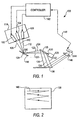
- the LPD 100 includes three lasers 102, 104, 106, each capable of emitting a beam of light 108, 110, 112 consisting of a unique color, such as red, green or blue.
- a unique color such as red, green or blue.
- the lasers 102, 104, 106 are arranged in a common plane 114 with the beams of light 108, 110, 112 being angularly directed relatively to one another to fall on a substantially common location 116 on a first scanning device, such as a first scanning mirror 118, from where they are reflected as beams of light 120, 122, 124.
- a first scanning device such as a first scanning mirror 118
- the first scanning mirror 118 oscillates on an axis 120 at a relatively high rate (e.g., 20-30 kHZ). Rotation or oscillation of the first scanning mirror 118 causes the beams of light 108, 110, 112 to be moved.
- the angular position of the first scanning mirror 118 alters, so to does the angle of reflection of the beams of light 120, 122, 124 from the first scanning mirror 118.
- the reflected beams of light 120, 122, 124 are scanned to produce movement of the beams of light 120, 122, 124 along one component of the two-dimensional display.
- the second component of the two-dimensional display is produced by a second scanning device, such as a mirror 126.
- the second mirror 126 is coupled to a motor 128 at a pivot point 130 so as to produce rotational or oscillating movement about an axis that is substantially orthogonal to the axis of rotation of the first mirror 118.
- the beams of light 120, 122, 124 are reflected off of the second mirror 126 as beams of light 132, 134, 136 and directed to a viewing surface 138.
- the viewing surface may take on any of a variety of forms.
- the second mirror oscillates or rotates at a relatively slow rate, as compared to the rate of the first mirror 118 (e.g., 60 hz).
- the beams of light 132, 134, 136 generally follow a path 140 on the display surface 138.
- the path 140 is similar in shape and concept to a raster scan commonly employed in cathode ray tube televisions and computer monitors.
- first and second scanning mirrors 118, 126 While the instant invention is described herein in the context of an embodiment that employs separate first and second scanning mirrors 118, 126, those skilled in the art will appreciate that a similar path 140 may be produced by using a single mirror.
- the single mirror would be capable of being moved about two axis of rotation to provide the fast and slow oscillating movements along two orthogonal axes.
- a controller 142 is provided to controllably energize the lasers 102, 104, 106 to effectively cause the beams of light 120, 122, 124 to be collinear, such that they may be reflected off of the second mirror 126 and delivered to the same point on the viewing surface 138 relatively independent of the distance of the viewing surface 138 from the second mirror 126.
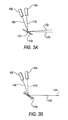
- the beams of light 120, 122 can be made to follow a single, common path (i.e., the beams of light 120, 122 are collinear). For example, if the laser 102 is energized at a first time t1, then the mirror 118 will be at a first position, as represented by the solid lines, and the beam of light 108 will reflect off of the mirror 118 as the beam of light 120.
- the mirror 118 will be at a second position, as represented by the dashed lines, and the beam of light 110 will reflect off of the mirror 118 as the beam of light 122.
- the mirror 118 will be in a position to accurately reflect the beam of light 122 along substantially the same path as the beam of light 120.
- the beams of light 120, 122 are substantially collinear, but are slightly displaced in time. That is, the beams of light 120, 122 will now both be projected onto substantially the same point on the display surface 13 8, but at slightly different times. However, owing to the persistence of the human eye, the variation in timing is not detectable. That is, in the case of the three laser system described in Figure 1 , each of the lasers 102, 104, 106 will controllably deliver laser light of a unique color and intensity to substantially the same point on the viewing surface 132 within a relatively short window of time.
- the human eye will not detect the three separate colors, bur rather will perceive a blending of the three light beams such that a consistent and desired hue appears at that point on the viewing surface. Those skilled in the art will appreciate that this process may be repeated numerous times along the path 140 to recreate a picture on the viewing surface 132.
- the routine begins at block 401 with the controller 142 determining the intensity for each of the lasers. That is, in order for a picture to be properly displayed, the controller 142 is capable of determining the hue of the picture at that small portion of the picture that is about to be projected onto the viewing surface. To reproduce the proper hue, the controller 142 determines the intensity for each of the lasers. This determination may be accomplished in any of a variety of conventional manners, such as via a look-up table, via a mathematical algorithm or the like.
- the controller 142 determines the time at which each of the lasers is to be energized.
- the determination of the timing may be accomplished in any of a variety of conventional manners, such as via a look-up table, via a mathematical algorithm or the like. This technique can be used during a calibration after manufacture. Ordinarily, this timing may be relatively fixed. That is, the timing may be established at the end of the manufacturing process by a factory technician, and thereafter, the controller may simply use these factory determined settings.
- a routine may be established to allow these settings to be altered as needed. That is a software routine may be included to project preselected tuning patterns (such as a cross pattern for each color laser) on the viewing surface. A service technician or consumer may then indicate to the controller (by depressing a preselected sequence of buttons) that the tuning patterns need to be adjusted to cause them to overlap properly. The controller 142 may then use the technician or consumer supplied information to alter the timing of the lasers.
- preselected tuning patterns such as a cross pattern for each color laser
- the controller 142 uses the determined timing and intensity for each of the lasers and controllably energizes the lasers to produce the desired hue at the present location on the viewing surface.
- the control routine 400 is continuously repeated for numerous points along the path 140 to effectively reproduce a picture on the viewing surface.
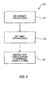
- a non-resonant scanning mirror 500 is activated using piezoelectric elements 502, 504.
- a characteristic stroke limitation of piezoelectric elements is overcome by applying a force developed by a piezoelectric element at a point very close to the axis of rotation of the mirror 500. Hence, relatively large scan angles can be achieved without relying on high mechanical Q factor.
- the mirror 500 may be formed from a substantially planar sheet of material 500, such as metals, ceramics, semiconductors or the like. Slots or grooves extending substantially through the sheet of material 500 divide the sheet of material 500 into two basic regions, a movable reflective region 502 and a base region 504, which in the illustrated embodiment substantially surrounds the movable reflective region 502.
- the movable reflective region 502 remains coupled to the base region 504 by a pair of split torsion hinges 506.
- the split torsion hinges 506 are formed by slots or grooves that extend substantially through the sheet of material 500 and are substantially aligned with an axis of rotation 508 of the movable reflective surface 502.
- the movable reflective surface 502 is generally free to rotate about the axis 508 so that laser light directed onto the movable reflective surface 502 may be reflected therefrom at various angles.
- Controllable positioning of the movable reflective surface 502 is accomplished by a set of piezoelectric elements 510, 512, 514,516.
- the piezoelectric elements 510, 512, 514, 516 extend between the base region 504 and a foundation, such as a printed circuit (PC) board 518.
- PC printed circuit
- the split hinges 506 provide a restoring force, which aids in returning the movable reflective region 502 to its initial unbiased position.
- Each hinge 506 also acts as a link, transmitting the force from the piezoelectric elements 510, 512, 514, 516 to the mirror 500. Since the forces are applied off-center, they generate torque, which forces the movable reflective region to rotate.
- the embodiment illustrated in Figure 5 is especially efficient when the mirror 500 is constructed using Micro-Electro-Mechanical Systems (MEMS) technology, so the split hinges 506 can be very narrow and the distance between the slots forming the hinges 506 may be very short.
- MEMS Micro-Electro-Mechanical Systems
- FIG. 6A a cross sectional end view of the mirror 500 is illustrated in various modes of operation.
- the piezoelectric elements have been energized in pairs 510, 512: 514,516 to apply forces in the directions indicated by the arrows 600, 602.
- the forces 600, 602 are applied to the base region 504 and are then transmitted to the movable reflective region 502 via the split hinges 506.
- the force applied through the split hinges 506 causes the movable reflective region 502 to rotate in a first direction, as indicated by the arrow 604.
- the amount of rotation may be accurately controlled.
- the amount of force delivered by the piezoelectric elements 510, 512, 514, 516 may be controlled by varying electrical parameters of a signal applied to the piezoelectric elements 510, 512, 514, 516.
- the amount of force generated by the piezoelectric elements 510, 512, 514, 516 may be controlled by varying the voltage, current, frequency, duty cycle, or a combination thereof. Additionally, it may be useful in some applications to apply unequal force through the various piezoelectric elements 510, 512, 514, 516.
- the piezoelectric elements have been energized in pairs 510, 512: 514, 516 in a manner to apply forces in the directions indicated by the arrows 600, 602, which are opposite to the forces shown in Figure 6A . Nevertheless, the forces 600, 602 are applied to the base region 504 and are then transmitted to the movable reflective region 502 via the split hinges 506. The force applied through the split hinges 506 causes the movable reflective region 502 to rotate in a second direction, as indicated by the arrow 604. By controlling the amount of force applied by the piezoelectric elements 510, 512, 514, 516 the amount of rotation may be accurately controlled.
- the amount of force delivered by the piezoelectric elements 510, 512, 514, 516 may be controlled by varying electrical parameters of a signal applied to the piezoelectric elements 510, S 12, 514, 516.
- the amount of force generated by the piezoelectric elements 510, 512, 514, 516 may be controlled by varying the voltage, current, frequency, duty cycle, or a combination thereof. Additionally, it may be useful in some applications to apply unequal force through the various piezoelectric elements 510, 512, 514, 516.
- the degree of rotation may be controlled by first energizing a first pair 510, 512 of the piezoelectric elements for a first range of rotation, and then energizing the second pair 514, 516 oppositely, and at the same time, to produce a second, greater range of rotation. That is, energizing the first pair 510, 512 may be useful to produce rotation in a range of 0-2°, whereas energizing both pairs 510, 512; 514, 516 oppositely and simultaneously may produce rotation in a range of 2-5°.
- varying energization schemes of the piezoelectric elements 510, 512, 514, 516 to produce various desirable rotational movement of the movable reflective region 502 may be employed.
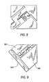
- Figures 7-9 alternative embodiments of the construction of the mirror 500 are shown.
- Figures 7-9 illustrate variations in the formation of the split hinges 506.
- Figures 7A and 7B illustrate a top view and an expanded top view of the mirror 500 having a plurality of hinges with offset, in accordance with the present invention. While the embodiment illustrated in Figure 7 shows two pairs of split hinges on each side of the mirror, those skilled in the art will appreciate that any number of hinge pairs with offset can be used. Further, the offset can have any value, starting from 0 and up to and, possibly, exceeding hinge width ( Fig. 7 shows offset roughly equal to hinge width).
- push-pads 800 which are used to attach the hinges, can be forked to allow some compliance or flexibility in the direction of hinge length and thus compensate for hinge stretching due to its twisting.
- push pads 900, 902 located on both sides of the hinges may be connected by bridges 904 to facilitate mirror handling and mounting. After the mirror is mounted, the bridges 904 may be either removed, or kept if they are sufficiently thin not to create substantial resistance.
Landscapes
- Physics & Mathematics (AREA)
- Optics & Photonics (AREA)
- General Physics & Mathematics (AREA)
- Engineering & Computer Science (AREA)
- Multimedia (AREA)
- Signal Processing (AREA)
- Mechanical Optical Scanning Systems (AREA)
- Transforming Electric Information Into Light Information (AREA)
- Mechanical Light Control Or Optical Switches (AREA)
Applications Claiming Priority (2)
| Application Number | Priority Date | Filing Date | Title |
|---|---|---|---|
| US10/837,037 US7446919B2 (en) | 2004-04-30 | 2004-04-30 | Piezoelectric actuated scanning mirror |
| PCT/US2005/013820 WO2005111692A1 (en) | 2004-04-30 | 2005-04-21 | Piezoelectric actuated scanning mirror |
Publications (2)
| Publication Number | Publication Date |
|---|---|
| EP1740997A1 EP1740997A1 (en) | 2007-01-10 |
| EP1740997B1 true EP1740997B1 (en) | 2014-08-20 |
Family
ID=34966452
Family Applications (1)
| Application Number | Title | Priority Date | Filing Date |
|---|---|---|---|
| EP05737855.6A Expired - Lifetime EP1740997B1 (en) | 2004-04-30 | 2005-04-21 | Piezoelectric actuated scanning mirror |
Country Status (7)
| Country | Link |
|---|---|
| US (1) | US7446919B2 (enExample) |
| EP (1) | EP1740997B1 (enExample) |
| JP (1) | JP4502401B2 (enExample) |
| KR (1) | KR20080036905A (enExample) |
| CN (1) | CN100447612C (enExample) |
| CA (1) | CA2560113A1 (enExample) |
| WO (1) | WO2005111692A1 (enExample) |
Families Citing this family (17)
| Publication number | Priority date | Publication date | Assignee | Title |
|---|---|---|---|---|
| US7182262B2 (en) * | 2003-03-13 | 2007-02-27 | Symbol Technologies, Inc. | Inertial drive scanning arrangement and method |
| KR100682958B1 (ko) * | 2006-01-10 | 2007-02-15 | 삼성전자주식회사 | 2축 마이크로 스캐너 |
| JP4400608B2 (ja) * | 2006-10-19 | 2010-01-20 | セイコーエプソン株式会社 | アクチュエータ、光スキャナ、および画像形成装置 |
| US7993005B2 (en) * | 2006-11-10 | 2011-08-09 | Seiko Epson Corporation | Color laser image generation |
| US8508098B2 (en) * | 2006-12-03 | 2013-08-13 | Maradin Technologies Ltd. | Gimbaled scanning micro-mirror actuation scheme and architecture |
| JP5286906B2 (ja) * | 2007-06-08 | 2013-09-11 | 大日本印刷株式会社 | 圧電ミラーデバイスとこれを用いた光学機器および圧電ミラーデバイスの製造方法 |
| NL1036321A1 (nl) * | 2007-12-20 | 2009-06-29 | Asml Netherlands Bv | Device control method and apparatus. |
| WO2009147654A1 (en) * | 2008-06-02 | 2009-12-10 | Maradin Technologies Ltd. | Gimbaled scanning micro-mirror apparatus |
| JP5539628B2 (ja) * | 2008-06-20 | 2014-07-02 | キヤノン電子株式会社 | 光走査用マイクロミラーデバイス、光走査装置、画像形成装置、表示装置および入力装置 |
| TWI438486B (zh) | 2010-08-17 | 2014-05-21 | Ind Tech Res Inst | 微振鏡裝置 |
| TWI408413B (zh) | 2011-02-25 | 2013-09-11 | Ind Tech Res Inst | 二維掃描反射裝置 |
| DE102011006595B4 (de) | 2011-03-31 | 2019-01-17 | Robert Bosch Gmbh | Mikromechanisches Bauteil und Herstellungsverfahren für ein mikromechanisches Bauteil |
| US9291816B2 (en) * | 2012-03-23 | 2016-03-22 | Panasonic intellectual property Management co., Ltd | Scanning mirror and scanning image display device |
| TWD166688S (zh) * | 2014-03-10 | 2015-03-21 | 虹光精密工業股份有限公司 | 掃描器 |
| US9690093B2 (en) * | 2014-10-15 | 2017-06-27 | Medlumics S.L. | Optical beam scanner |
| CN105403997A (zh) * | 2015-11-19 | 2016-03-16 | 苏州工业园区纳米产业技术研究院有限公司 | 一种压电驱动二维扫描微镜 |
| CN109491078A (zh) * | 2019-01-07 | 2019-03-19 | 南京理工大学 | 一种高精度微扫描装置 |
Family Cites Families (20)
| Publication number | Priority date | Publication date | Assignee | Title |
|---|---|---|---|---|
| US5029975A (en) | 1990-01-24 | 1991-07-09 | The Mitre Corporation | Despeckling screen utilizing optical fibers and method of reducing interference using same |
| US5208880A (en) * | 1992-04-30 | 1993-05-04 | General Electric Company | Microdynamical fiber-optic switch and method of switching using same |
| EP0704138B1 (en) | 1993-02-03 | 2001-08-01 | Nitor | Method and apparatus for image projection |
| US5311321A (en) | 1993-04-22 | 1994-05-10 | Corporation For Laser Optics Research | Laser video imaging system with pulse backtrack and method |
| US6304237B1 (en) | 1996-11-29 | 2001-10-16 | Corporation For Laser Optics Research | Monochromatic R,G,B laser light source display system and method |
| US5915063A (en) * | 1997-01-15 | 1999-06-22 | Colbourne; Paul | Variable optical attenuator |
| US6201629B1 (en) * | 1997-08-27 | 2001-03-13 | Microoptical Corporation | Torsional micro-mechanical mirror system |
| US6140979A (en) | 1998-08-05 | 2000-10-31 | Microvision, Inc. | Scanned display with pinch, timing, and distortion correction |
| US6937221B2 (en) | 1998-08-05 | 2005-08-30 | Microvision, Inc. | Scanned beam display |
| JP3552601B2 (ja) * | 1998-11-16 | 2004-08-11 | 日本ビクター株式会社 | 光偏向子及びこれを用いた表示装置 |
| US6018408A (en) | 1999-03-26 | 2000-01-25 | Samsung Electronics Co., Ltd. | Laser projection display apparatus |
| US6384406B1 (en) * | 1999-08-05 | 2002-05-07 | Microvision, Inc. | Active tuning of a torsional resonant structure |
| US6515781B2 (en) | 1999-08-05 | 2003-02-04 | Microvision, Inc. | Scanned imaging apparatus with switched feeds |
| US6593677B2 (en) * | 2000-03-24 | 2003-07-15 | Onix Microsystems, Inc. | Biased rotatable combdrive devices and methods |
| US6330102B1 (en) * | 2000-03-24 | 2001-12-11 | Onix Microsystems | Apparatus and method for 2-dimensional steered-beam NxM optical switch using single-axis mirror arrays and relay optics |
| US6489934B1 (en) | 2000-07-07 | 2002-12-03 | Judah Klausner | Cellular phone with built in optical projector for display of data |
| IL159677A0 (en) | 2001-07-06 | 2004-06-20 | Explay Ltd | An image projecting device and method |
| US6710680B2 (en) * | 2001-12-20 | 2004-03-23 | Motorola, Inc. | Reduced size, low loss MEMS torsional hinges and MEMS resonators employing such hinges |
| JP3905539B2 (ja) * | 2002-08-14 | 2007-04-18 | 富士通株式会社 | トーションバーを備えるマイクロ揺動素子 |
| JP4898121B2 (ja) | 2003-01-08 | 2012-03-14 | エクスプレイ エルティーディー | 画像投影装置 |
-
2004
- 2004-04-30 US US10/837,037 patent/US7446919B2/en not_active Expired - Fee Related
-
2005
- 2005-04-21 JP JP2007510828A patent/JP4502401B2/ja not_active Expired - Fee Related
- 2005-04-21 EP EP05737855.6A patent/EP1740997B1/en not_active Expired - Lifetime
- 2005-04-21 KR KR1020067022714A patent/KR20080036905A/ko not_active Ceased
- 2005-04-21 WO PCT/US2005/013820 patent/WO2005111692A1/en not_active Ceased
- 2005-04-21 CN CNB2005800131079A patent/CN100447612C/zh not_active Expired - Fee Related
- 2005-04-21 CA CA002560113A patent/CA2560113A1/en not_active Abandoned
Also Published As
| Publication number | Publication date |
|---|---|
| CN100447612C (zh) | 2008-12-31 |
| KR20080036905A (ko) | 2008-04-29 |
| WO2005111692A1 (en) | 2005-11-24 |
| CN1947051A (zh) | 2007-04-11 |
| JP2007535706A (ja) | 2007-12-06 |
| US7446919B2 (en) | 2008-11-04 |
| EP1740997A1 (en) | 2007-01-10 |
| US20050243446A1 (en) | 2005-11-03 |
| CA2560113A1 (en) | 2005-11-24 |
| JP4502401B2 (ja) | 2010-07-14 |
Similar Documents
| Publication | Publication Date | Title |
|---|---|---|
| EP1740997B1 (en) | Piezoelectric actuated scanning mirror | |
| US5185660A (en) | Actuated mirror optical intensity modulation | |
| EP0497891B1 (en) | Television with apertures to modulate beam intensity | |
| AU646425B2 (en) | Television display system for modulating projected beams' intensity | |
| KR101196179B1 (ko) | 요동장치, 상기 요동장치를 이용한 광스캐닝장치, 영상표시장치 및 요동장치의 제어방법 | |
| US9712812B2 (en) | Method and device for projecting an image | |
| US20190236762A1 (en) | Device and Method for Projecting an Image | |
| CN103686027B (zh) | 图像显示装置和图像扫描装置 | |
| US20020075380A1 (en) | Apparatus for outputting laser beam | |
| US20120194891A1 (en) | Optical beam control based on flexure actuation with positioning sensing and servo control | |
| WO2012072125A1 (en) | A method for projecting an image | |
| JP5234514B2 (ja) | 画像形成装置 | |
| WO2005067311A1 (en) | Method and apparatus for aligning a plurality of lasers in an electronic display device | |
| US12235180B2 (en) | Phase alignment system and method of oscillating mirror | |
| WO2005119309A1 (ja) | 反射ミラー製作方法および反射ミラー | |
| KR20020034764A (ko) | 마이크로 구동 장치 | |
| EP0740180A1 (en) | Apparatus for directing light | |
| KR100851071B1 (ko) | 주사 주기를 제어하는 광변조기를 이용한 디스플레이 방법및 그 장치 | |
| JP2004117836A (ja) | ミラーデバイス、光スイッチ、電子機器およびミラーデバイス駆動方法 | |
| JP2004294959A (ja) | 静電型アクチュエータ | |
| KR19990042777A (ko) | 투사형 화상표시장치의 ama 패널 위치조정장치 |
Legal Events
| Date | Code | Title | Description |
|---|---|---|---|
| PUAI | Public reference made under article 153(3) epc to a published international application that has entered the european phase |
Free format text: ORIGINAL CODE: 0009012 |
|
| 17P | Request for examination filed |
Effective date: 20061030 |
|
| AK | Designated contracting states |
Kind code of ref document: A1 Designated state(s): DE FR GB IT |
|
| DAX | Request for extension of the european patent (deleted) | ||
| RBV | Designated contracting states (corrected) |
Designated state(s): DE FR GB IT |
|
| 17Q | First examination report despatched |
Effective date: 20091207 |
|
| RAP1 | Party data changed (applicant data changed or rights of an application transferred) |
Owner name: MICROVISION, INC. |
|
| GRAP | Despatch of communication of intention to grant a patent |
Free format text: ORIGINAL CODE: EPIDOSNIGR1 |
|
| INTG | Intention to grant announced |
Effective date: 20140219 |
|
| RAP1 | Party data changed (applicant data changed or rights of an application transferred) |
Owner name: MICROVISION, INC. |
|
| GRAS | Grant fee paid |
Free format text: ORIGINAL CODE: EPIDOSNIGR3 |
|
| GRAA | (expected) grant |
Free format text: ORIGINAL CODE: 0009210 |
|
| AK | Designated contracting states |
Kind code of ref document: B1 Designated state(s): DE FR GB IT |
|
| REG | Reference to a national code |
Ref country code: GB Ref legal event code: FG4D |
|
| REG | Reference to a national code |
Ref country code: DE Ref legal event code: R096 Ref document number: 602005044531 Country of ref document: DE Effective date: 20140925 |
|
| REG | Reference to a national code |
Ref country code: FR Ref legal event code: PLFP Year of fee payment: 11 |
|
| PG25 | Lapsed in a contracting state [announced via postgrant information from national office to epo] |
Ref country code: IT Free format text: LAPSE BECAUSE OF FAILURE TO SUBMIT A TRANSLATION OF THE DESCRIPTION OR TO PAY THE FEE WITHIN THE PRESCRIBED TIME-LIMIT Effective date: 20140820 |
|
| REG | Reference to a national code |
Ref country code: DE Ref legal event code: R097 Ref document number: 602005044531 Country of ref document: DE |
|
| PLBE | No opposition filed within time limit |
Free format text: ORIGINAL CODE: 0009261 |
|
| STAA | Information on the status of an ep patent application or granted ep patent |
Free format text: STATUS: NO OPPOSITION FILED WITHIN TIME LIMIT |
|
| 26N | No opposition filed |
Effective date: 20150521 |
|
| PGFP | Annual fee paid to national office [announced via postgrant information from national office to epo] |
Ref country code: GB Payment date: 20150415 Year of fee payment: 11 Ref country code: DE Payment date: 20150414 Year of fee payment: 11 |
|
| PGFP | Annual fee paid to national office [announced via postgrant information from national office to epo] |
Ref country code: FR Payment date: 20150408 Year of fee payment: 11 |
|
| REG | Reference to a national code |
Ref country code: DE Ref legal event code: R119 Ref document number: 602005044531 Country of ref document: DE |
|
| GBPC | Gb: european patent ceased through non-payment of renewal fee |
Effective date: 20160421 |
|
| REG | Reference to a national code |
Ref country code: FR Ref legal event code: ST Effective date: 20161230 |
|
| PG25 | Lapsed in a contracting state [announced via postgrant information from national office to epo] |
Ref country code: DE Free format text: LAPSE BECAUSE OF NON-PAYMENT OF DUE FEES Effective date: 20161101 Ref country code: FR Free format text: LAPSE BECAUSE OF NON-PAYMENT OF DUE FEES Effective date: 20160502 Ref country code: GB Free format text: LAPSE BECAUSE OF NON-PAYMENT OF DUE FEES Effective date: 20160421 |