EP1739649A1 - Passive matrix display with means for compensating resistive losses - Google Patents
Passive matrix display with means for compensating resistive losses Download PDFInfo
- Publication number
- EP1739649A1 EP1739649A1 EP05300526A EP05300526A EP1739649A1 EP 1739649 A1 EP1739649 A1 EP 1739649A1 EP 05300526 A EP05300526 A EP 05300526A EP 05300526 A EP05300526 A EP 05300526A EP 1739649 A1 EP1739649 A1 EP 1739649A1
- Authority
- EP
- European Patent Office
- Prior art keywords
- line
- column
- electrode
- emitters
- electrodes
- Prior art date
- Legal status (The legal status is an assumption and is not a legal conclusion. Google has not performed a legal analysis and makes no representation as to the accuracy of the status listed.)
- Withdrawn
Links
Images

Classifications
-
- G—PHYSICS
- G09—EDUCATION; CRYPTOGRAPHY; DISPLAY; ADVERTISING; SEALS
- G09G—ARRANGEMENTS OR CIRCUITS FOR CONTROL OF INDICATING DEVICES USING STATIC MEANS TO PRESENT VARIABLE INFORMATION
- G09G3/00—Control arrangements or circuits, of interest only in connection with visual indicators other than cathode-ray tubes
- G09G3/20—Control arrangements or circuits, of interest only in connection with visual indicators other than cathode-ray tubes for presentation of an assembly of a number of characters, e.g. a page, by composing the assembly by combination of individual elements arranged in a matrix no fixed position being assigned to or needed to be assigned to the individual characters or partial characters
- G09G3/22—Control arrangements or circuits, of interest only in connection with visual indicators other than cathode-ray tubes for presentation of an assembly of a number of characters, e.g. a page, by composing the assembly by combination of individual elements arranged in a matrix no fixed position being assigned to or needed to be assigned to the individual characters or partial characters using controlled light sources
- G09G3/30—Control arrangements or circuits, of interest only in connection with visual indicators other than cathode-ray tubes for presentation of an assembly of a number of characters, e.g. a page, by composing the assembly by combination of individual elements arranged in a matrix no fixed position being assigned to or needed to be assigned to the individual characters or partial characters using controlled light sources using electroluminescent panels
- G09G3/32—Control arrangements or circuits, of interest only in connection with visual indicators other than cathode-ray tubes for presentation of an assembly of a number of characters, e.g. a page, by composing the assembly by combination of individual elements arranged in a matrix no fixed position being assigned to or needed to be assigned to the individual characters or partial characters using controlled light sources using electroluminescent panels semiconductive, e.g. using light-emitting diodes [LED]
- G09G3/3208—Control arrangements or circuits, of interest only in connection with visual indicators other than cathode-ray tubes for presentation of an assembly of a number of characters, e.g. a page, by composing the assembly by combination of individual elements arranged in a matrix no fixed position being assigned to or needed to be assigned to the individual characters or partial characters using controlled light sources using electroluminescent panels semiconductive, e.g. using light-emitting diodes [LED] organic, e.g. using organic light-emitting diodes [OLED]
- G09G3/3216—Control arrangements or circuits, of interest only in connection with visual indicators other than cathode-ray tubes for presentation of an assembly of a number of characters, e.g. a page, by composing the assembly by combination of individual elements arranged in a matrix no fixed position being assigned to or needed to be assigned to the individual characters or partial characters using controlled light sources using electroluminescent panels semiconductive, e.g. using light-emitting diodes [LED] organic, e.g. using organic light-emitting diodes [OLED] using a passive matrix
-
- G—PHYSICS
- G09—EDUCATION; CRYPTOGRAPHY; DISPLAY; ADVERTISING; SEALS
- G09G—ARRANGEMENTS OR CIRCUITS FOR CONTROL OF INDICATING DEVICES USING STATIC MEANS TO PRESENT VARIABLE INFORMATION
- G09G2320/00—Control of display operating conditions
- G09G2320/02—Improving the quality of display appearance
- G09G2320/0223—Compensation for problems related to R-C delay and attenuation in electrodes of matrix panels, e.g. in gate electrodes or on-substrate video signal electrodes
-
- G—PHYSICS
- G09—EDUCATION; CRYPTOGRAPHY; DISPLAY; ADVERTISING; SEALS
- G09G—ARRANGEMENTS OR CIRCUITS FOR CONTROL OF INDICATING DEVICES USING STATIC MEANS TO PRESENT VARIABLE INFORMATION
- G09G2320/00—Control of display operating conditions
- G09G2320/02—Improving the quality of display appearance
- G09G2320/0233—Improving the luminance or brightness uniformity across the screen
-
- G—PHYSICS
- G09—EDUCATION; CRYPTOGRAPHY; DISPLAY; ADVERTISING; SEALS
- G09G—ARRANGEMENTS OR CIRCUITS FOR CONTROL OF INDICATING DEVICES USING STATIC MEANS TO PRESENT VARIABLE INFORMATION
- G09G3/00—Control arrangements or circuits, of interest only in connection with visual indicators other than cathode-ray tubes
- G09G3/20—Control arrangements or circuits, of interest only in connection with visual indicators other than cathode-ray tubes for presentation of an assembly of a number of characters, e.g. a page, by composing the assembly by combination of individual elements arranged in a matrix no fixed position being assigned to or needed to be assigned to the individual characters or partial characters
- G09G3/22—Control arrangements or circuits, of interest only in connection with visual indicators other than cathode-ray tubes for presentation of an assembly of a number of characters, e.g. a page, by composing the assembly by combination of individual elements arranged in a matrix no fixed position being assigned to or needed to be assigned to the individual characters or partial characters using controlled light sources
- G09G3/30—Control arrangements or circuits, of interest only in connection with visual indicators other than cathode-ray tubes for presentation of an assembly of a number of characters, e.g. a page, by composing the assembly by combination of individual elements arranged in a matrix no fixed position being assigned to or needed to be assigned to the individual characters or partial characters using controlled light sources using electroluminescent panels
- G09G3/32—Control arrangements or circuits, of interest only in connection with visual indicators other than cathode-ray tubes for presentation of an assembly of a number of characters, e.g. a page, by composing the assembly by combination of individual elements arranged in a matrix no fixed position being assigned to or needed to be assigned to the individual characters or partial characters using controlled light sources using electroluminescent panels semiconductive, e.g. using light-emitting diodes [LED]
- G09G3/3208—Control arrangements or circuits, of interest only in connection with visual indicators other than cathode-ray tubes for presentation of an assembly of a number of characters, e.g. a page, by composing the assembly by combination of individual elements arranged in a matrix no fixed position being assigned to or needed to be assigned to the individual characters or partial characters using controlled light sources using electroluminescent panels semiconductive, e.g. using light-emitting diodes [LED] organic, e.g. using organic light-emitting diodes [OLED]
- G09G3/3275—Details of drivers for data electrodes
Definitions
- the invention relates to passive matrix electroluminescent diode panels for displaying images and a method for controlling these panels.
- the diodes of such panels can be controlled current or voltage.
- the current control as described for example in WO03 / 107318 , requires current generators that are economically disadvantageous; this current control method is also penalized by high parasitic capacitance charging times each time a new line of diodes to be addressed is selected, unless a pre-charge device is added, which increases still the cost of the panel.
- the voltage control which is more economical and allows the quasi-instantaneous load parasitic capacitances, requires on the other hand compensations ohmic losses along the supply electrodes.
- the document W02004 / 027743 proposes to add, at the head of each column electrode, a device for controlling injected charges (product of current by duration) which is slaved to a voltage setpoint addressed to a diode of this column, which diode is also selected by a line electrode.
- a load control device and its servocontrol at the head of each column is economically disadvantageous.
- An object of the invention is to avoid the aforementioned drawbacks.
- the subject of the invention is a passive matrix image display or lighting device comprising an array of light emitters, an array of line electrodes and a network of column electrodes for feeding in voltage these emitters, and means able to compensate, without video processing, and at least partially, the differences in connection resistance of these emitters via these electrodes.
- these compensation means are able to compensate for both differences in column resistances and differences in line resistances.
- connection resistance of an emitter is the sum of the resistance between one of the output terminals of the generator able to supply it and the point of connection of this emitter to its line electrode, and of on the other hand, the resistance between the other of the output terminals of this generator and the point of connection of this emitter to its column electrode. Any other definition of the connection resistance of the transmitters can be retained without departing from the invention, as long as it does not change the differences between the connection resistances of these transmitters.
- the "point" of line and column connection of a transmitter generally corresponds to a portion of the line electrode and a portion of the column electrode that form two feed electrodes of that emitter.
- the "point" of supply of the line electrode and the column electrode generally corresponds to one end of these electrodes.
- the so-called "line” resistance of a transmitter being defined as the resistance of the line electrode to which this emitter is connected, taken between the supply point of this line electrode and the connection point of the transmitter.
- said compensation means are able to compensate for the differences between the so-called “line” resistors of the emitters of each line.
- the subject of the invention is also a method for controlling an image display or lighting device according to the invention, characterized in that ... if the "line" resistance difference between two transmitters which are connected to the same row electrode and to two adjacent column electrodes of the panel is approximately constant irrespective of the column electrodes and line electrodes considered, and is worth R r , ...
- the emitters of the panel can be divided into several sets according to their emission color and / or their electrical characteristics: for example, a first set of emitters of a first type which are able to emit a red light, a second set of emitters emitters of a second type which are able to emit a green light, a third type of emitters of a third type that are able to emit a blue light.
- Each type of transmitter has different electrical characteristics, including current-voltage characteristics.
- the compensation means are adapted to ensure an identical voltage between the terminals of each transmitter of this group.
- the documents EP 1439518 and WO 2004/114273 disclose ohmic loss compensation means in the LED connecting electrodes which are essentially applicable to active matrix image display panels, wherein the electrodes of one of the arrays are common to all the diodes and form usually an upper layer of the panel.
- the electrodes of the other network are integrated into the matrix of the panel, as in the case of passive matrix panels. Consequently, the compensation means described in the documents EP 1439518 and WO 2004/114273 , only compensate the ohmic losses in a single array of electrodes, whereas the invention relates here passive matrix panels with two power supply electrode arrays and allows to compensate the ohmic losses simultaneously for both electrode networks.
- the documents JP10-112391 and JP07-295509 do not give any teaching on the compensation of the ohmic losses simultaneously for the two networks of electrodes which feed the emitters.
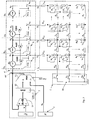
- the device conventionally comprises a display panel which is provided with a network of light emitters, here electroluminescent organic diodes, known in themselves, each feedable between two terminals, a network of N row electrodes Y 1 , Y 2 , ..., Y j , ..., Y N , and a network of P column electrodes X 1 , X 2 ,..., X i ,... X P , to supply transmitters; the terminals of each transmitter are connected on the one hand to a line electrode, to a line connection point, and on the other hand to a column electrode, to a column connection point.
- the display panel does not include control circuits for each transmitter: it is therefore a passive matrix panel.
- the device comprises supply means which comprise in particular a voltage generator 2 adapted to deliver a voltage V 0 between two output terminals: only one terminal is shown in the figures, the other terminal being connected to a ground line.
- supply means comprise in particular a voltage generator 2 adapted to deliver a voltage V 0 between two output terminals: only one terminal is shown in the figures, the other terminal being connected to a ground line.
- the device also comprises means 5 capable of successively selecting each line of transmitters, by connecting, with the aid of a controllable line-selection switch S 1 , S 2 , ..., S N , a point of supplying the line electrode Y 1 , Y 2 ,..., Y N , to which these emitters are connected to the output terminal of the generator 2 which is connected to a ground line via a common line electrode 55 and another line of mass.
- the feed points of the line electrodes are located at the ends of these electrodes on the same side of the panel.
- the device also comprises means 4 capable of addressing transmitters of the same line so that they emit light, by simultaneously connecting, with the aid of controllable column addressing switches A 1 , A 2 , A 3 , ..., A P , a feed point of each of the column electrodes X 1 , X 2 ,..., X P , to which these emitters are connected to the other output terminal of the generator 2 via a common column electrode 44.
- the feed points of the column electrodes are located at the ends of these columns. electrodes on the same side of the panel.
- the control of the switches A 1 , A 2 , A 3 ,..., A P is adapted to control, in particular according to video data, the supply duration of the emitters so as to obtain control of the panel by modulation. of duration. This command is referenced "PWM"("Pulse Width Modulation”) in the figures.
- Controlling the closing of the switches A i and S j therefore makes it possible to connect the generator 2 to any emitter E ij so that it emits light.
- the current flowing through the transmitter depends on the values of i and j, that is to say on the position of this emitter on the panel.
- the device also comprises means capable of compensating at least partially the differences in connection resistance R Eij emitters, two embodiments of which will now be described.
- the generator 2 are associated with column compensation means 3 able to compensate for differences in connection resistance called “column".
- the so-called “column” resistance of an emitter is defined as the resistance of the column electrode to which this emitter is connected, taken between the supply point of this column electrode and the point of connection of this emitter on this column electrode; for a transmitter E ij , this column resistance is therefore R co + (j-1) ⁇ R c .
- each column corresponds to the same primary color, and the columns of different primary colors are alternated.
- Such resistance compensation means of the column electrodes are particularly simple and economical to implement and allow the voltage control of the emitters of the panel, which is advantageous because it limits the preload times, which allows to increase by the transmission durations when displaying the images, and thus to improve the luminous performances of the panel.
- this device makes it possible to use economic column control means which integrate globally for the whole panel only three voltage generators according to this device, instead of a current generator by column electrode as in the current drivers of the device. walk.
- This device is also much simpler and more economical to implement than specific video data processing devices capable of compensating for differences in connection resistance, especially since such video processing often involves a loss of definition of the levels of gray of each color.
- compensating means that are able to compensate not only the differences in column resistance as before, but also the differences in resistances. say "line”.
- the so-called “line” resistance of a transmitter is defined as the resistance of the line electrode to which this emitter is connected, taken between the supply point of this line electrode and the point of connection of this emitter on this line electrode; for a transmitter E ij , this line resistance is therefore R ro + (i-1) ⁇ R r .
- a difficulty for the compensation of differences in line resistance comes from the fact that the different resistances R r between the successive points of connection of transmitters on the same line electrode are generally traversed by different currents, at least when several transmitters of this line are activated simultaneously, ie when the "PWM" command simultaneously closes several addressing switches.
- V inc (j-1) ⁇ R c .
- the compensation means here comprise on the one hand the same column compensation means 3 as those previously described in the first embodiment, but also elements added to the addressing means 4 'which are able to partially compensate for the differences in line resistors, as described below.
- the common feed electrode of the columns 44 is interrupted: between the successive connection points of this electrode to a switch controlling the emission duration A 1 , A 2 , A 3 , ..., A P , there are in this embodiment of voltage generators G 0 , G 1 , ..., G p-1 , which are programmed using commands; each generator G i is able to deliver a voltage ⁇ V i proportional to its control C i .
- each adder Add (i-1) comprises two inputs and an output: one of the inputs is connected to the control (value 1 or 0) of the switch A i , which is able to connect the common column electrode 44 to the column electrode X i ; the other input is connected to the output of adders Add (i) of the next column if it exists; the output of this adders Add (i-1) is connected to the input of the adder Add (i-2) of the previous column if it exists, and also forms the command C (i-1) of the generator G ( i-1) which is interposed on the common column electrode between the connection point of the switch A (i-1) and that of the switch A i .
- V 0 + j - 1 For each emitter E ij , we now have the equation: V 0 + j - 1 .
- V 0 - V d R vs ⁇ o + R d ⁇ i d .
- i d (V 0 -V d ) / (R co + R d ).
- the present invention is applicable to all types of light emitter panels, especially those that are current-controllable like light-emitting diodes.
Landscapes
- Engineering & Computer Science (AREA)
- Physics & Mathematics (AREA)
- Computer Hardware Design (AREA)
- General Physics & Mathematics (AREA)
- Theoretical Computer Science (AREA)
- Control Of Indicators Other Than Cathode Ray Tubes (AREA)
Abstract
Description
L'invention concerne les panneaux de diodes électroluminescentes à matrice passive pour affichage d'images et une méthode de pilotage de ces panneaux. Lorsqu'elles sont modulées en durée (« PWM », ou « Pulse Width Modulation » en langue anglaise), les diodes de tels panneaux peuvent être commandées en courant ou en tension.The invention relates to passive matrix electroluminescent diode panels for displaying images and a method for controlling these panels. When modulated in time ("PWM" or "Pulse Width Modulation" in English), the diodes of such panels can be controlled current or voltage.
La commande en courant, telle que décrite par exemple dans
La commande en tension, qui est plus économique et permet la charge quasi-instantanée des capacités parasites, nécessite par contre des compensations des pertes ohmiques le long des électrodes d'alimentation.The voltage control, which is more economical and allows the quasi-instantaneous load parasitic capacitances, requires on the other hand compensations ohmic losses along the supply electrodes.
Pour compenser ces pertes, ainsi d'ailleurs que la dispersion des caractéristiques électriques entre les différentes diodes du panneau, le document
Un but de l'invention est d'éviter les inconvénients précités.An object of the invention is to avoid the aforementioned drawbacks.
A cet effet, l'invention a pour objet un dispositif d'affichage d'images ou d'éclairage comprenant :
- un panneau d'affichage ou d'éclairage qui comporte :
- a) un réseau d'émetteurs de lumière disposés en lignes et en colonnes,
- b) un réseau de N électrodes de ligne, et un réseau de P électrodes de colonne,
.... chaque émetteur étant connecté d'une part à une desdites électrodes de ligne, en un point de connexion de ligne, et d'autre part à une desdites électrodes de colonne, en un point de connexion de colonne, de manière à pouvoir être alimenté entre cette électrode de ligne et cette électrode de colonne,
- des moyens d'alimentation des émetteurs qui comportent :
- a) au moins un générateur de tension apte à délivrer une tension d'alimentation entre deux bornes de sortie,
- b) des moyens aptes à sélectionner successivement chaque ligne d'émetteurs, en reliant un point d'alimentation de l'électrode de ligne à laquelle ces émetteurs sont connectés à l'une des bornes de sortie de l'au moins un générateur,
- c) des moyens aptes à adresser des émetteurs d'une même ligne pour qu'ils émettent de la lumière, en reliant simultanément un point d'alimentation de chacune des électrodes de colonne auxquelles ces émetteurs sont connectés à l'autre borne de sortie de l'au moins un générateur,
- d) des moyens aptes à compenser au moins partiellement les différences de résistance de connexion des émetteurs,
- a billboard or lighting panel that includes:
- a) a network of light emitters arranged in rows and columns,
- b) a network of N row electrodes, and a network of P column electrodes,
each transmitter being connected firstly to one of said line electrodes, at a line connection point, and secondly to one of said column electrodes, at a column connection point, so as to be able to be fed between this line electrode and this column electrode,
- transmitter power supply means comprising:
- a) at least one voltage generator capable of delivering a supply voltage between two output terminals,
- b) means capable of successively selecting each line of emitters, by connecting a feed point of the line electrode to which these emitters are connected to one of the output terminals of the at least one generator,
- c) means able to send emitters of the same line so that they emit light, by simultaneously connecting a feed point of each of the column electrodes to which these emitters are connected to the other output terminal of the at least one generator,
- d) means capable of compensating at least partially the differences in connection resistance of the transmitters,
En résumé, l'invention a pour objet un dispositif d'affichage d'images ou d'éclairage à matrice passive comprenant un réseau d'émetteurs de lumière, un réseau d'électrodes de ligne et un réseau d'électrodes de colonne pour alimenter en tension ces émetteurs, et des moyens aptes à compenser, sans traitement vidéo, et au moins partiellement, les différences de résistance de connexion de ces émetteurs via ces électrodes. De préférence, ces moyens de compensation sont aptes à compenser à la fois les différences de résistances de colonne et les différences de résistances de ligne.In summary, the subject of the invention is a passive matrix image display or lighting device comprising an array of light emitters, an array of line electrodes and a network of column electrodes for feeding in voltage these emitters, and means able to compensate, without video processing, and at least partially, the differences in connection resistance of these emitters via these electrodes. Preferably, these compensation means are able to compensate for both differences in column resistances and differences in line resistances.
La résistance de connexion d'un émetteur est la somme d'une part de la résistance entre l'une des bornes de sortie du générateur apte à l'alimenter et le point de connexion de cet émetteur à son électrode de ligne, et d'autre part de la résistance entre l'autre des bornes de sortie de ce générateur et le point de connexion de cet émetteur à son électrode de colonne. Toute autre définition de la résistance de connexion des émetteurs peut être retenue sans se départir de l'invention, du moment qu'elle ne change pas les différences entre les résistances de connexion de ces émetteurs.The connection resistance of an emitter is the sum of the resistance between one of the output terminals of the generator able to supply it and the point of connection of this emitter to its line electrode, and of on the other hand, the resistance between the other of the output terminals of this generator and the point of connection of this emitter to its column electrode. Any other definition of the connection resistance of the transmitters can be retained without departing from the invention, as long as it does not change the differences between the connection resistances of these transmitters.
Le « point » de connexion de ligne et de colonne d'un émetteur correspond en général à une partie de l'électrode de ligne et à une partie de l'électrode de colonne qui forment deux électrodes d'alimentation de cet émetteur.The "point" of line and column connection of a transmitter generally corresponds to a portion of the line electrode and a portion of the column electrode that form two feed electrodes of that emitter.
Le « point » d'alimentation de l'électrode de ligne et de l'électrode de colonne correspond en général à une extrémité de ces électrodes.The "point" of supply of the line electrode and the column electrode generally corresponds to one end of these electrodes.
De préférence, la résistance dite « de ligne » d'un émetteur étant définie comme la résistance de l'électrode de ligne à laquelle cet émetteur est connecté, prise entre le point d'alimentation de cette électrode de ligne et le point de connexion de cet émetteur sur cette électrode de ligne, lesdits moyens de compensation sont aptes à compenser les différences entre les résistances dites « de ligne » des émetteurs de chaque ligne.Preferably, the so-called "line" resistance of a transmitter being defined as the resistance of the line electrode to which this emitter is connected, taken between the supply point of this line electrode and the connection point of the transmitter. this emitter on this line electrode, said compensation means are able to compensate for the differences between the so-called "line" resistors of the emitters of each line.
De préférence :
- ledit panneau est à matrice passive ;
- lesdits émetteurs sont des diodes électroluminescentes, notamment, organiques.
- said panel is passive matrix;
- said emitters are electroluminescent diodes, especially organic diodes.
L'invention a également pour objet un procédé de pilotage d'un dispositif d'affichage d'images ou d'éclairage selon l'invention caractérisé en ce que ... si la différence de résistance « de colonne » entre deux émetteurs qui sont connectés à une même électrode de colonne et à deux électrodes de ligne adjacentes du panneau est approximativement constante quelles que soient les électrodes de colonne et les électrodes de ligne considérées, et vaut Rc,
- à l'aide desdits moyens de sélection, on sélectionne successivement, pendant une période de sélection, chaque ligne du panneau, d'une ligne à la suivante adjacente,
- et, lorsqu'une ligne d'émetteurs est sélectionnée, à l'aide desdits moyens d'adressage, on adresse des émetteurs de cette ligne pour qu'ils émettent de la lumière pendant une partie au moins de ladite période de sélection,
... et, si id est le courant circulant dans un quelconque desdits émetteurs qui émet de la lumière, - à l'aide desdits moyens de compensation, on incrémente ladite tension d'alimentation d'une valeur Vinc = Rc × id lorsque l'on passe d'une ligne quelconque sélectionnée à la suivante adjacente.
- with the aid of said selection means, each line of the panel is successively selected, during a selection period, from one line to the next adjacent one,
- and, when a line of transmitters is selected, using said means addressing, emitters of this line are sent to emit light during at least part of said selection period,
... and, if i d is the current flowing in any one of the emitters that emits light, - with the aid of said compensating means, said supply voltage is incremented by a value V inc = R c × i d when passing from one selected line to the next adjacent one.
L'invention a également pour objet un procédé de pilotage d'un dispositif d'affichage d'images ou d'éclairage selon l'invention, caractérisé en ce que ... si la différence de résistance « de ligne » entre deux émetteurs qui sont connectés à une même électrode de ligne et à deux électrodes de colonne adjacentes du panneau est approximativement constante quelles que soient les électrodes de colonne et les électrodes de ligne considérées, et vaut Rr, ... pendant qu'on adresse des émetteurs de ladite ligne sélectionnée, entre deux électrodes de colonne adjacentes X(i-1), Xi, on applique un incrément de tension ΔV(i-1) approximativement égal à C(i-1) × V'inc, où V'inc = Rr × id, où C(i-1) ![]()
![]()
Quelque soient les émetteurs du panneau qui sont alimentés par le générateur, la tension aux bornes de chacun de ces émetteurs est alors approximativement identique. On parvient ainsi, sans traitement complémentaire des données vidéo et à l'aide d'une méthode très simple et économique à implémenter, à compenser globalement et de manière très performante les différences de résistance de connexion des émetteurs, quelques soient les images affichées par le dispositif.Whatever the emitters of the panel that are powered by the generator, the voltage across each of these emitters is then approximately identical. Thus, without further processing of the video data and with the aid of a very simple and inexpensive method to be implemented, it is possible to compensate globally and in a very efficient manner the differences in connection resistance of the transmitters, whatever the images displayed by the device.
Les émetteurs du panneau peuvent être répartis en plusieurs ensembles selon leur couleur d'émission et/ou leurs caractéristiques électriques : par exemple, un premier ensemble d'émetteurs d'un premier type qui sont aptes à émettre une lumière rouge, un deuxième ensemble d'émetteurs d'un deuxième type qui sont aptes à émettre une lumière verte, un troisième type d'émetteurs d'un troisième type qui sont aptes à émettre une lumière bleue. Chaque type d'émetteurs présente des caractéristiques électriques différentes, notamment des caractéristiques courant-tension. Selon l'invention, quelque soit le groupe d'émetteurs du même ensemble d'émetteurs du même type, les moyens de compensation sont adaptés pour assurer une tension identique entre les bornes de chaque émetteur de ce groupe. A supposer qu'au sein de chaque ensemble, les émetteurs présentent les mêmes caractéristiques d'intensité d'émission lumineuse pour cette tension identique commune, on obtient ainsi selon l'invention une très grande homogénéité d'émission lumineuse sur toute la surface du panneau, ce qui, dans le cas d'un panneau d'affichage, est très favorable à la qualité d'affichage des images.The emitters of the panel can be divided into several sets according to their emission color and / or their electrical characteristics: for example, a first set of emitters of a first type which are able to emit a red light, a second set of emitters emitters of a second type which are able to emit a green light, a third type of emitters of a third type that are able to emit a blue light. Each type of transmitter has different electrical characteristics, including current-voltage characteristics. According to the invention, whatever the group of transmitters of the same set of transmitters of the same type, the compensation means are adapted to ensure an identical voltage between the terminals of each transmitter of this group. Assuming that, within each set, the emitters have the same luminous emission intensity characteristics for this common identical voltage, a very high luminous emission homogeneity is obtained according to the invention over the entire surface of the panel. which, in the case of a billboard, is very favorable to the quality of display of the images.
Les documents
L'invention sera mieux comprise à la lecture de la description qui va suivre, donnée à titre d'exemple non limitatif, et en référence aux figures annexées sur lesquelles :
- la figure 1 illustre un premier mode de réalisation de l'invention adapté pour compenser les différences de résistance de colonne,
- la figure 2 illustre un deuxième mode de réalisation de l'invention adapté pour compenser à la fois les différences de résistance de colonne et les différences de résistance de ligne.
- FIG. 1 illustrates a first embodiment of the invention adapted to compensate for differences in column resistance,
- FIG. 2 illustrates a second embodiment of the invention adapted for compensate for both differences in column resistance and differences in line resistance.
On va maintenant décrire les éléments communs aux deux modes de réalisation de l'invention en se référant aux figures 1 et 2.The elements common to the two embodiments of the invention will now be described with reference to FIGS. 1 and 2.
Le dispositif selon l'invention comprend d'une manière classique un panneau d'affichage qui est doté d'un réseau d'émetteurs de lumière, ici des diodes organiques électroluminescentes, connues en elles-mêmes, chacune alimentable entre deux bornes, un réseau de N électrodes de ligne Y1, Y2, ..., Yj, ..., YN, et un réseau de P électrodes de colonne X1, X2, ..., Xi,... XP, pour alimenter des émetteurs ; les bornes de chaque émetteur sont connectées d'une part à une électrode de ligne, en un point de connexion de ligne, et d'autre part à une électrode de colonne, en un point de connexion de colonne. Le panneau d'affichage ne comprend pas de circuits de commande pour chaque émetteur : il s'agit donc d'un panneau à matrice passive.The device according to the invention conventionally comprises a display panel which is provided with a network of light emitters, here electroluminescent organic diodes, known in themselves, each feedable between two terminals, a network of N row electrodes Y 1 , Y 2 , ..., Y j , ..., Y N , and a network of P column electrodes X 1 , X 2 ,..., X i ,... X P , to supply transmitters; the terminals of each transmitter are connected on the one hand to a line electrode, to a line connection point, and on the other hand to a column electrode, to a column connection point. The display panel does not include control circuits for each transmitter: it is therefore a passive matrix panel.
Le dispositif comprend des moyens d'alimentation qui comprennent notamment un générateur de tension 2 adapté pour délivrer une tension V0 entre deux bornes de sortie : une seule borne est représentée sur les figures, l'autre borne étant reliée à une ligne de masse.The device comprises supply means which comprise in particular a
Le dispositif comprend également des moyens 5 aptes à sélectionner successivement chaque ligne d'émetteurs, en reliant, à l'aide d'un interrupteur commandable de sélection de ligne S1, S2, ..., SN, un point d'alimentation de l'électrode de ligne Y1, Y2, ..., YN, à laquelle ces émetteurs sont connectés à la borne de sortie du générateur 2 qui est reliée à une ligne de masse, via une électrode commune de ligne 55 et une autre ligne de masse. Les points d'alimentation des électrodes de ligne sont situés aux extrémités de ces électrodes d'un même côté du panneau.The device also comprises
Le dispositif comprend également des moyens 4 aptes à adresser des émetteurs d'une même ligne pour qu'ils émettent de la lumière, en reliant simultanément, à l'aide d'interrupteurs commandables d'adressage de colonne A1, A2, A3,..., AP, un point d'alimentation de chacune des électrodes de colonne X1, X2, ..., XP, auxquelles ces émetteurs sont connectés à l'autre borne de sortie du générateur 2 via une électrode commune de colonne 44. Les points d'alimentation des électrodes de colonne sont situés aux extrémités de ces électrodes d'un même côté du panneau. La commande des interrupteurs A1, A2, A3,..., AP est adaptée pour contrôler, en fonction, notamment, de données vidéo, la durée d'alimentation des émetteurs de manière à obtenir un pilotage du panneau par modulation de durée. Cette commande est référencée « PWM » (« Pulse Width Modulation ») sur les figures.The device also comprises
La commande de la fermeture des interrupteurs Ai et Sj permet donc de relier au générateur 2 un émetteur quelconque Eij de manière à ce qu'il émette de la lumière.Controlling the closing of the switches A i and S j therefore makes it possible to connect the
On définit la résistance de connexion d'un émetteur quelconque Eij comme la somme d'une part de la résistance entre la borne de sortie du générateur 2 qui est reliée à la masse et le point de connexion de cet émetteur à son électrode de ligne Yj, et d'autre part de la résistance entre l'autre borne de sortie de ce générateur 2 et le point de connexion de cet émetteur à son électrode de colonne Xi. ;
- soit Rco la résistance entre l'extrémité d'une électrode de colonne et le premier point de connexion d'un émetteur sur cette électrode ;
- soit Rro la résistance entre l'extrémité d'une électrode de ligne et le premier point de connexion d'un émetteur sur cette électrode ;
- soit Rc la résistance d'une électrode de colonne entre deux points successifs de connexion d'émetteurs sur cette électrode ; ainsi, la différence de résistance de connexion entre deux émetteurs, qui sont reliés à une même électrode de colonne et à deux électrodes de ligne adjacentes vaut Rc ;
- soit Rr la résistance d'une électrode de ligne entre deux points successifs de connexion d'émetteurs sur cette électrode ; ainsi, la différence de résistance de connexion entre deux émetteurs, qui sont reliés à une même électrode de ligne et à deux électrodes de colonne adjacentes vaut Rr ;
- let R co be the resistance between the end of a column electrode and the first point of connection of an emitter on this electrode;
- let R ro be the resistance between the end of a line electrode and the first point of connection of a transmitter on this electrode;
- or R c the resistance of a column electrode between two successive emitter connection points on this electrode; thus, the difference in connection resistance between two emitters, which are connected to the same column electrode and to two adjacent line electrodes is R c ;
- let R r be the resistance of a line electrode between two successive emitter connection points on this electrode; thus, the difference in connection resistance between two transmitters, which are connected to one and the same row electrode and to two adjacent column electrodes is R r ;
La résistance de connexion RE11 de l'émetteur E11 de la première ligne et de la première colonne est donc RE11 = Rco + Rro.The connection resistance R E11 of the emitter E 11 of the first line and of the first column is therefore R E11 = R co + R ro .
La résistance de connexion RE12 de l'émetteur E12 de la deuxième ligne et de la première colonne est donc RE12 = Rc + Rco + Rro.The connection resistance R E12 of the emitter E 12 of the second line and of the first column is therefore R E12 = R c + R co + R ro .
La résistance de connexion RE21 de l'émetteur E21 de la première ligne et de la deuxième colonne est donc RE21 = Rr + Rco + Rro.The connection resistance R E21 of the emitter E 21 of the first line and the second column is therefore R E21 = R r + R co + R ro .
Par extension, la résistance de connexion REij de l'émetteur Eij de la ligne j et de la colonne i est donc REij = (i-1) × Rr + (j-1) × Rc + Rco + Rro.By extension, the connection resistance R Eij of the transmitter E ij of the line j and the column i is therefore R Eij = (i-1) × R r + (j-1) × R c + R co + R ro .
Soit Rd et Vd définis de manière à ce que la relation entre la tension VE d'une diode quelconque du panneau et le courant i qui circule dans cette diode est telle que VE = Vd + Rd × id, cette relation étant valable dans le domaine de fonctionnement de la diode lors du fonctionnement du panneau.Let R d and V d be defined in such a way that the relation between the voltage V E of any diode of the panel and the current i which flows in this diode is such that V E = V d + R d × i d , this relation being valid in the operating domain of the diode during operation of the panel.
Si Vo est la tension délivrée par le générateur 2, si l'on intègre la résistance des interrupteurs d'adressage de colonne Ai et celle de l'électrode commune de colonne 44 à la valeur de la résistance Rco, si l'on intègre la résistance des interrupteurs de sélection de ligne Sj et celle de l'électrode commune de ligne 55 à la valeur de la résistance Rro, alors, lorsqu'un seul émetteur Eij quelconque du panneau est alimenté par le générateur 2, et en l'absence de moyens de compensation selon l'invention, le courant Iij qui traverse cet émetteur Eij vaut alors : Iij = (Vo - Vd)/ (Rd + REij) = (Vo-Vd)/ [Rd + (i-1) × Rr + (j-1)×Rc+Rco+Rro].If V o is the voltage delivered by the
On voit donc que, en l'absence de moyens de compensation selon l'invention, le courant traversant l'émetteur dépend des valeurs de i et de j, c'est-à-dire de la position de cet émetteur sur le panneau.It can therefore be seen that, in the absence of compensation means according to the invention, the current flowing through the transmitter depends on the values of i and j, that is to say on the position of this emitter on the panel.
C'est pourquoi, selon l'invention, le dispositif comprend également des moyens aptes à compenser au moins partiellement les différences de résistance de connexion REij des émetteurs, dont deux modes de réalisation vont maintenant être décrits.Therefore, according to the invention, the device also comprises means capable of compensating at least partially the differences in connection resistance R Eij emitters, two embodiments of which will now be described.
En référence à la figure 1, selon le premier mode de réalisation de l'invention, au générateur 2 sont adjoints des moyens de compensation de colonne 3 aptes compenser les différences de résistance de connexion dites « de colonne ». La résistance dite « de colonne » d'un émetteur est définie comme la résistance de l'électrode de colonne à laquelle cet émetteur est connecté, prise entre le point d'alimentation de cette électrode de colonne et le point de connexion de cet émetteur sur cette électrode de colonne ; pour un émetteur Eij, cette résistance de colonne vaut donc Rco + (j-1) × Rc.Referring to Figure 1, according to the first embodiment of the invention, the
Les moyens de compensation de colonne 3 comprennent :
un sommateur 31 doté de deux entrées à additionner et d'une sortie délivrant la somme des signaux d'entrée ; l'un des signaux d'entrée est Vinc, dont la valeur sera définie ultérieurement ;- une mémoire 32 apte à stocker la valeur délivrée par le sommateur 31 ;
- un multiplexeur « MUX » 33 doté de deux entrées, dont l'une est alimentée par la mémoire 32, l'autre par le signal de tension Vo, et d'une sortie adaptée pour délivrer l'une des deux entrées en fonction d'une donnée de commande. La sortie du multiplexeur 33 est reliée d'une part à l'électrode commune de colonne 44, et d'autre part à l'une des entrées du sommateur 31.
- an
adder 31 having two inputs to be added and an output delivering the sum of the input signals; one of the input signals is V inc , the value of which will be defined later; - a
memory 32 able to store the value delivered by theadder 31; - a multiplexer "MUX" 33 having two inputs, one of which is powered by the
memory 32, the other by the voltage signal V o , and an output adapted to deliver one of the two inputs as a function of a control data. The output of themultiplexer 33 is connected on the one hand to thecommon column electrode 44, and on the other hand to one of the inputs of theadder 31.
En fonctionnement, le dispositif fonctionne de la manière suivante :
- on sélectionne la première ligne en fermant l'interrupteur S1, et on envoie simultanément un signal de 1ère ligne (marqué « 1st line » sur la figure) au multiplexeur 33 ; les émetteurs de la première ligne étant alors connectés à la première électrode de ligne Y1, le multiplexeur 33 délivre une tension Vo à l'électrode commune de colonne 44 ; les interrupteurs A1, A2, A3,..., AP sont maintenus ouverts ou fermés pendant une durée contrôlée en fonction des données vidéo à adresser aux émetteurs de cette première ligne ; à chaque interrupteur fermé Ai, correspond un émetteur Ei1 qui est alors alimenté par le générateur 2 pour émettre de la lumière ; sur le circuit de chaque émetteur alimenté, on a donc : Vo = (Rco + Rd) id + Vd, ou id.= (V0 -Vd)/(Rco + Rd).
- au déclenchement d'un signal de changement de ligne (« line + 1 ») appliqué à la mémoire 22, la somme de la tension Vo délivrée par le multiplexeur 23 et de Vinc est envoyée à l'électrode commune de ligne 44 pour alimenter un deuxième groupe d'émetteurs connectés à la deuxième électrode de ligne Y2 ; sur le circuit de chaque émetteur alimenté de cette ligne, on a donc : Vo + Vinc = (Rco + Rd + Rc) i'd + Vd . En prenant Vinc = Rc × id, on en déduit que i'd = id. On constate donc que la résistance d'électrode de colonne apportée par le changement de ligne est compensée par l'incrément de tension d'alimentation Vinc, du moment que l'on choisit Vinc = Rc × id.
- the first line is selected by closing the switch S1, and simultaneously sends a signal of one line period (labeled "1st line" in the figure) to the
multiplexer 33; the emitters of the first line then being connected to the first line electrode Y 1 , themultiplexer 33 delivers a voltage V o to thecommon column electrode 44; the switches A 1 , A 2 , A 3 ,..., A P are kept open or closed for a controlled duration depending on the video data to be sent to the transmitters of this first line; each closed switch A i corresponds to a transmitter E i1 which is then powered by thegenerator 2 to emit light; on the circuit of each emitter fed, we thus have: V o = (R co + R d ) i d + V d , where i d = (V 0 -V d ) / (R co + R d ). - at the triggering of a line-change signal ("line + 1") applied to the memory 22, the sum of the voltage V o delivered by the multiplexer 23 and of V inc is sent to the
common line electrode 44 for supplying a second group of transmitters connected to the second line electrode Y 2 ; on the circuit of each emitter supplied with this line, we thus have: V o + V inc = (R co + R d + R c ) i ' d + V d . Taking V inc = R c × i d , we deduce that i ' d = i d . It can therefore be seen that the column electrode resistance provided by the line change is compensated by the supply voltage increment V inc , as long as V inc = R c × i d is chosen.
Le même avantage s'applique aux autres lignes du panneau, en appliquant, à chaque fois que l'on passe d'une ligne à la suivante, le même incrément de tension Vinc.The same advantage applies to the other lines of the panel, applying, each time one goes from one line to the next, the same voltage increment V inc .
Ainsi, globalement, on pilote le dispositif comme suit :
- à l'aide des moyens de sélection 5, on sélectionne successivement, pendant une période de sélection, chaque ligne du panneau, d'une ligne à la suivante adjacente,
- et, lorsqu'une ligne d'émetteurs est sélectionnée, à l'aide des moyens d'adressage 4, on adresse des émetteurs de cette ligne pour qu'ils émettent de la lumière pendant une partie de cette période de sélection correspondant à la donnée vidéo à leur adresser,
- et, si id est le courant circulant dans un quelconque desdits émetteurs qui émet de la lumière pendant cette partie de période de sélection, à l'aide des moyens de compensation de
colonne 3, on incrémente la tension d'alimentation délivrée par le générateur 2 d'une valeur Rc × id lorsque l'on passe d'une ligne quelconque sélectionnée à la suivante adjacente.
- using the selection means 5, one selects successively, during a selection period, each line of the panel, from one line to the next adjacent,
- and, when a line of transmitters is selected, using the addressing
means 4, transmitters of this line are addressed to emit light during part of this selection period corresponding to the data. video to send them, - and, if i d is the current flowing in any one of said emitters which emits light during this selection period portion, using the column compensation means 3, the supply voltage supplied by the generator is incremented 2 of a value R c × i d when passing from one selected line to the next adjacent one.
Dans le cas où le panneau est trichrome et est doté de trois ensembles d'émetteurs, un ensemble pour chaque couleur primaire d'émission, il conviendra d'implémenter des moyens de compensation de colonne 3 pour chaque ensemble d'émetteurs. Généralement, chaque colonne correspond à une même couleur primaire, et les colonnes de couleurs primaires différentes sont alternées.In the case where the panel is trichromatic and has three sets of transmitters, one set for each primary color of emission, it will be necessary to implement column compensation means 3 for each set of transmitters. Generally, each column corresponds to the same primary color, and the columns of different primary colors are alternated.
De tels moyens de compensation de résistance des électrodes de colonne sont particulièrement simples et économiques à implémenter et permettent le pilotage en tension des émetteurs du panneau, ce qui est avantageux car on limite les durées de précharge, ce qui permet d'augmenter d'autant les durées d'émission lors de l'affichage des images, et donc d'améliorer les performances lumineuses du panneau. Par ailleurs ce dispositif permet d'utiliser des moyens de commande de colonne économiques n'intégrant globalement pour tout le panneau que trois générateurs de tension selon ce dispositif, au lieu d'un générateur de courant par électrode de colonne comme dans les drivers actuels du marché. Ce dispositif est également beaucoup plus simple et économique à mettre en oeuvre que des dispositifs spécifiques de traitement des données vidéo aptes à compenser les différences de résistances de connexion, d'autant qu'un tel traitement vidéo implique souvent une perte de définition des niveaux de gris de chaque couleur.Such resistance compensation means of the column electrodes are particularly simple and economical to implement and allow the voltage control of the emitters of the panel, which is advantageous because it limits the preload times, which allows to increase by the transmission durations when displaying the images, and thus to improve the luminous performances of the panel. Moreover, this device makes it possible to use economic column control means which integrate globally for the whole panel only three voltage generators according to this device, instead of a current generator by column electrode as in the current drivers of the device. walk. This device is also much simpler and more economical to implement than specific video data processing devices capable of compensating for differences in connection resistance, especially since such video processing often involves a loss of definition of the levels of gray of each color.
En référence à la figure 2, selon le deuxième mode de réalisation de l'invention, au même générateur 2 sont adjoints des moyens de compensation qui sont aptes à compenser non seulement les différences de résistance de colonne comme précédemment, mais également les différences de résistances dites « de ligne ». La résistance dite « de ligne » d'un émetteur est définie comme la résistance de l'électrode de ligne à laquelle cet émetteur est connecté, prise entre le point d'alimentation de cette électrode de ligne et le point de connexion de cet émetteur sur cette électrode de ligne ; pour un émetteur Eij, cette résistance de ligne vaut donc Rro + (i-1) × Rr.With reference to FIG. 2, according to the second embodiment of the invention, at the
Une difficulté pour la compensation des différences de résistance de ligne vient de ce que les différentes résistances Rr entre les points successifs de connexion d'émetteurs sur la même électrode de ligne sont généralement parcourus par des courants différents, du moins lorsque plusieurs émetteurs de cette ligne sont activés simultanément, c'est-à-dire lorsque la commande « PWM » ferme simultanément plusieurs interrupteurs d'adressage.A difficulty for the compensation of differences in line resistance comes from the fact that the different resistances R r between the successive points of connection of transmitters on the same line electrode are generally traversed by different currents, at least when several transmitters of this line are activated simultaneously, ie when the "PWM" command simultaneously closes several addressing switches.
Si l'on désigne par VAL_Ak la valeur 1 ou 0 de la commande d'un interrupteur d'adressage de l'électrode de colonne Xi (1 = fermé et émetteur Ekj actif, 0 = ouvert et émetteur Ekj éteint), si l'on désigne par iij le courant traversant chaque émetteur Eij de la ligne j qui est activé, le courant total circulant au niveau du point d'alimentation (c'est-à-dire l'extrémité) de l'électrode de ligne Yj sera alors égal à ![]()
![]()
![]()
![]()
En l'absence de moyens de compensation des résistances de ligne, pour chaque émetteur Eij, on a donc l'équation : 
Selon les moyens de compensation de colonne précédemment décrits, on a Vinc = (j-1) × Rc.According to the column compensation means described above, there is V inc = (j-1) × R c .
On a donc autant d'équations que d'inconnues. La résolution d'un tel système donne en général des valeurs différentes pour les courants qui traversent les émetteurs activés de la ligne j. Or, la fonction des moyens de compensation est d'obtenir des valeurs identiques de ces courants.We therefore have as many equations as unknowns. The resolution of such a system generally gives different values for the currents that flow through the activated transmitters of the line j. However, the function of the compensation means is to obtain identical values of these currents.
Les moyens de compensation comprennent ici d'une part les mêmes moyens de compensation de colonne 3 que ceux précédemment décrits dans le premier mode de réalisation, mais également des éléments ajoutés aux moyens d'adressage 4' qui sont aptes à compenser partiellement les différences de résistances de ligne, comme décrit ci-après.The compensation means here comprise on the one hand the same column compensation means 3 as those previously described in the first embodiment, but also elements added to the addressing means 4 'which are able to partially compensate for the differences in line resistors, as described below.
Comme l'indique la figure 2, l'électrode commune d'alimentation des colonnes 44 est interrompue : entre les points de connexion successifs de cette électrode à un interrupteur de contrôle de la durée d'émission A1, A2, A3,..., AP, on trouve dans ce mode de réalisation des générateurs de tension G0, G1, ..., Gp-1, qui sont programmés à l'aide de commandes ; chaque générateur Gi est apte à délivrer une tension ΔVi proportionnelle à sa commande Ci.As indicated in FIG. 2, the common feed electrode of the
En outre, les éléments nouveaux ajoutés aux moyens d'adressage 4' comprennent des additionneurs Add0, Add1, ..., Add(p-2), Add(p-1). Chaque additionneur Add(i-1) comprend deux entrées et une sortie : l'une des entrées est reliée à la commande (valeur 1 ou 0) de l'interrupteur Ai, qui est apte à relier l'électrode commune de colonne 44' à l'électrode de colonne Xi ; l'autre entrée est reliée à la sortie de l'additionneurs Add(i) de la colonne suivante si elle existe ; la sortie de cet additionneurs Add(i-1) est reliée à l'entrée de l'additionneur Add(i-2) de la colonne précédente si elle existe, et forme également la commande C(i-1) du générateur G(i-1) qui est intercalé sur l'électrode commune de colonne entre le point de connexion de l'interrupteur A(i-1) et celui du l'interrupteur Ai.In addition, the new elements added to the addressing means 4 'include adders Add0, Add1, ..., Add (p-2), Add (p-1). Each adder Add (i-1) comprises two inputs and an output: one of the inputs is connected to the control (
On va maintenant expliquer le fonctionnement de la compensation des différences de résistances de lignes.We will now explain the operation of the compensation of the differences in line resistances.
Pour chaque émetteur Eij , on a donc maintenant l'équation : 
Si, selon l'invention, chaque générateur délivre une tension ΔVk = Ck × V'inc , si id est le courant parcourant chaque émetteur activé lorsqu'on a compensation des résistances de connexion de colonne et de ligne, et si V'inc = Rr × id, et sachant que, de la description des moyens de compensation de lignes qui est décrite ci-dessus, il découle que la commande Ck de chaque générateur Gk vaut ![]()

![]()
En simplifiant une première fois : 
En simplifiant une deuxième fois : ![]()
![]()
Et, comme dans le premier mode de réalisation, id.= (V0 -Vd)/(Rco + Rd).And, as in the first embodiment, i d = (V 0 -V d ) / (R co + R d ).
On vérifie donc que, grâce aux moyens de compensation selon l'invention tels que précédemment décrits, on compense cette fois globalement les variations de résistance globale de connexion des émetteurs, c'est-à-dire à la fois les résistances de colonne et les résistance de ligne, quelques soient les données vidéo affichées par le dispositif. Avantageusement, ce résultat est obtenu sans traitement complémentaire des données vidéo, contrairement aux moyens de compensation décrits dans l'art antérieur. Les moyens mis en oeuvre pour cette compensation sont particulièrement simples et économiques.It is therefore verified that, thanks to the compensation means according to the invention as previously described, this time overall the global transmitter connection resistance variations, that is to say both the column resistances and the resistors, are compensated overall. line resistance, whatever the video data displayed by the device. Advantageously, this result is obtained without additional processing of the video data, unlike the compensation means described in the prior art. The means used for this compensation are particularly simple and economical.
Ainsi, globalement, on pilote le dispositif comme suit :
- à l'aide des moyens de sélection 5, on sélectionne successivement, pendant une période de sélection, chaque ligne du panneau, d'une ligne à la suivante adjacente,
- et, lorsqu'une ligne d'émetteurs est sélectionnée, à l'aide des moyens d'adressage 4, on adresse des émetteurs de cette ligne pour qu'ils émettent de la lumière pendant une partie au moins de cette période de sélection,
- et, si id est le courant circulant dans un quelconque desdits émetteurs qui émet de la lumière pendant cette partie de période de sélection, pendant qu'on adresse des émetteurs de ladite ligne sélectionnée, entre deux électrodes de colonne adjacentes X(i-1), Xi, on applique un incrément de tension ΔV(i-1) égal à

- et, à l'aide des moyens de compensation de
colonne 3, on incrémente la tension d'alimentation délivrée par le générateur 2 d'une valeur Rc × id lorsque l'on passe d'une ligne quelconque sélectionnée à la suivante adjacente. Quelque soient les émetteurs du panneau qui sont alimentés par le générateur, la tension aux bornes de chacun de ces émetteurs est alors approximativement identique. On parvient ainsi, sans traitement complémentaire des données vidéo et à l'aide d'une méthode très simple et économique à implémenter, à compenser totalement les différences de résistance de connexion des émetteurs, quelques soient les images affichées par le dispositif.
- using the selection means 5, one successively selects, during a selection period, each line of the panel, from one line to the next adjacent,
- and, when an emitter line is selected, using the addressing
means 4, transmitters of this line are addressed to emit light during at least part of this selection period, - and, if i d is the current flowing in any one of said emitters that emits light during that selection period portion, while emitters of said selected line are addressed between two adjacent column electrodes X ( i-1 ), X i , a voltage increment ΔV (i-1) equal to
- and, using the column compensation means 3, the supply voltage supplied by the
generator 2 is incremented by a value R c × i d when passing from one selected line to the next adjacent one. . Whatever the emitters of the panel that are powered by the generator, the voltage across each of these emitters is then approximately identical. Thus, without further processing of the video data and using a very simple and inexpensive method to implement, it is possible to completely compensate the differences in the connection resistance of the transmitters, whatever the images displayed by the device.
La présente invention s'applique à tous les types de panneaux d'émetteurs de lumière, notamment ceux qui sont pilotables en courant comme les diodes électroluminescentes.The present invention is applicable to all types of light emitter panels, especially those that are current-controllable like light-emitting diodes.
Claims (6)
.... chaque émetteur (Eij) étant connecté d'une part à une desdites électrodes de ligne (Yj), en un point de connexion de ligne, et d'autre part à une desdites électrodes de colonne (Xi), en un point de connexion de colonne, de manière à pouvoir être alimenté entre cette électrode de ligne (Yj) et cette électrode de colonne (Xi),
... la résistance dite « de colonne » d'un émetteur (Eij) étant définie comme la résistance de l'électrode de colonne (Xi) à laquelle cet émetteur est connecté, prise entre le point d'alimentation de cette électrode de colonne et le point de connexion de cet émetteur sur cette électrode de colonne (Xi), lesdits moyens de compensation sont aptes à compenser les différences entre les résistances dites « de colonne » des émetteurs de chaque colonne.
each emitter (E ij ) being connected firstly to one of said line electrodes (Y j ), at a line connection point, and secondly to one of said column electrodes (X i ) at a column connection point, so that it can be fed between this line electrode (Y j ) and this column electrode (X i ),
... the so-called "column" resistance of a transmitter (E ij ) being defined as the resistance of the column electrode (X i ) to which this emitter is connected, taken between the supply point of this electrode column and the point of connection of this emitter on this column electrode (X i ), said compensation means are able to compensate for the differences between the so-called "column" resistors of the emitters of each column.
lesdits moyens de compensation sont aptes à compenser les différences entre les résistances dites « de ligne » des émetteurs de chaque ligne.Device according to claim 1, characterized in that the so-called "line" resistance of a transmitter (E ij ) being defined as the resistance of the line electrode (Y j ) to which this emitter is connected, taken between the feed point of this line electrode and the connection point of this emitter on this line electrode (Y j ),
said compensation means are able to compensate for the differences between the so-called "line" resistors of the emitters of each line.
... et, si id est le courant circulant dans un quelconque desdits émetteurs qui émet de la lumière,
... and, if i d is the current flowing in any one of the emitters that emits light,
... si la différence de résistance « de ligne » entre deux émetteurs qui sont connectés à une même électrode de ligne et à deux électrodes de colonne adjacentes du panneau est approximativement constante quelles que soient les électrodes de colonne (Xi) et les électrodes de ligne (Yj) considérées, et vaut Rr,
... pendant qu'on adresse des émetteurs de ladite ligne sélectionnée, entre deux électrodes de colonne adjacentes (X(i-1), Xi), on applique un incrément de tension ΔV(i-1) approximativement égal à C(i-1) × V'inc, où V'inc = Rr × id, où
... if the "line" resistance difference between two transmitters that are connected to the same row electrode and two adjacent column electrodes of the panel is approximately constant regardless of the column electrodes (X i ) and the electrodes of line (Y j ) considered, and is worth R r ,
while sending transmitters of said selected line between two adjacent column electrodes (X ( i-1 ), X i ), a voltage increment ΔV (i-1) approximately equal to C is applied ( i-1) × V ' inc , where V' inc = R r × i d , where
Priority Applications (1)
| Application Number | Priority Date | Filing Date | Title |
|---|---|---|---|
| EP05300526A EP1739649A1 (en) | 2005-06-28 | 2005-06-28 | Passive matrix display with means for compensating resistive losses |
Applications Claiming Priority (1)
| Application Number | Priority Date | Filing Date | Title |
|---|---|---|---|
| EP05300526A EP1739649A1 (en) | 2005-06-28 | 2005-06-28 | Passive matrix display with means for compensating resistive losses |
Publications (1)
| Publication Number | Publication Date |
|---|---|
| EP1739649A1 true EP1739649A1 (en) | 2007-01-03 |
Family
ID=34981734
Family Applications (1)
| Application Number | Title | Priority Date | Filing Date |
|---|---|---|---|
| EP05300526A Withdrawn EP1739649A1 (en) | 2005-06-28 | 2005-06-28 | Passive matrix display with means for compensating resistive losses |
Country Status (1)
| Country | Link |
|---|---|
| EP (1) | EP1739649A1 (en) |
Cited By (1)
| Publication number | Priority date | Publication date | Assignee | Title |
|---|---|---|---|---|
| CN111034359A (en) * | 2017-08-30 | 2020-04-17 | 平面系统公司 | Current controller for an output stage of LED driver circuitry |
Citations (3)
| Publication number | Priority date | Publication date | Assignee | Title |
|---|---|---|---|---|
| US6400348B1 (en) * | 1999-06-25 | 2002-06-04 | Koninklijke Philips Electronics N.V. | Active matrix electroluminescent display device |
| US20020149547A1 (en) * | 2001-01-29 | 2002-10-17 | Robertson John A. | Transparent programmable LED display panel and method |
| US6580407B1 (en) * | 1994-06-08 | 2003-06-17 | Canon Kabushiki Kaisha | Electron-beam generating device having plurality of cold cathode elements, method of driving said device and image forming apparatus applying same |
-
2005
- 2005-06-28 EP EP05300526A patent/EP1739649A1/en not_active Withdrawn
Patent Citations (3)
| Publication number | Priority date | Publication date | Assignee | Title |
|---|---|---|---|---|
| US6580407B1 (en) * | 1994-06-08 | 2003-06-17 | Canon Kabushiki Kaisha | Electron-beam generating device having plurality of cold cathode elements, method of driving said device and image forming apparatus applying same |
| US6400348B1 (en) * | 1999-06-25 | 2002-06-04 | Koninklijke Philips Electronics N.V. | Active matrix electroluminescent display device |
| US20020149547A1 (en) * | 2001-01-29 | 2002-10-17 | Robertson John A. | Transparent programmable LED display panel and method |
Non-Patent Citations (2)
| Title |
|---|
| JUAN C-J ET AL: "A VOLTAGE COMPENSATION CONTROLLER FOR LIGHTING PASSIVE MATRIX ORGANIC LIGHT EMITTING DIODES PANELS", 2003 SID INTERNATIONAL SYMPOSIUM DIGEST OF TECHNICAL PAPERS. BALTIMORE, MD, MAY 20 - 22, 2003; [SID INTERNATIONAL SYMPOSIUM DIGEST OF TECHNICAL PAPERS], SAN JOSE, CA : SID, US, 20 May 2003 (2003-05-20), pages 1134 - 1137, XP001174237 * |
| JUAN C-J ET AL: "A VOLTAGE-COMPENSATED DRIVER FOR LIGHTING PMOLEDS PANELS", IEEE TRANSACTIONS ON CONSUMER ELECTRONICS, IEEE SERVICE CENTER, NEW YORK, NY, US, vol. 49, no. 2, 1 May 2003 (2003-05-01), pages 263 - 268, XP001171285, ISSN: 0098-3063, DOI: 10.1109/TCE.2003.1209512 * |
Cited By (2)
| Publication number | Priority date | Publication date | Assignee | Title |
|---|---|---|---|---|
| CN111034359A (en) * | 2017-08-30 | 2020-04-17 | 平面系统公司 | Current controller for an output stage of LED driver circuitry |
| CN111034359B (en) * | 2017-08-30 | 2023-01-10 | 平面系统公司 | Current controller for an output stage of LED driver circuitry |
Similar Documents
| Publication | Publication Date | Title |
|---|---|---|
| EP1644913B1 (en) | Display device and control circuit for a light modulator | |
| EP1851747B1 (en) | Pixel addressing circuit and method of controlling such circuit | |
| FR2864678A1 (en) | ELECTROLUMINESCENCE DISPLAY DEVICE AND METHOD OF CONTROLLING THE SAME | |
| FR2884639A1 (en) | ACTIVE MATRIX IMAGE DISPLAY PANEL, THE TRANSMITTERS OF WHICH ARE POWERED BY POWER-DRIVEN POWER CURRENT GENERATORS | |
| FR2846843A1 (en) | VEHICLE LAMP IGNITION CIRCUIT | |
| FR2869717A1 (en) | Electroluminescent display device has data driver with output channels which supply data signals to data electrode lines, and multiplexer for coupling output channels of data driver to data electrode lines | |
| FR2626706A1 (en) | INTEGRATED MATRIX DISPLAY ASSEMBLY | |
| FR2733852A1 (en) | METHOD AND CIRCUIT FOR CONTROLLING DISPLAY DEVICE | |
| FR2734076A1 (en) | FIELD EMISSION DEVICE HAVING A TRANSIENT CURRENT SOURCE | |
| WO2000002183A1 (en) | Screen control with cathodes having low electronic affinity | |
| EP1964094B1 (en) | Method for controlling a display panel by capacitive coupling | |
| EP2046021B1 (en) | Pixel matrix with ohmic drop compensation on the power supplies | |
| EP0078193B1 (en) | Control circuit for an ac plasma panel | |
| EP1739649A1 (en) | Passive matrix display with means for compensating resistive losses | |
| EP1700290B1 (en) | Image display screen and method of addressing said screen | |
| EP1771838B1 (en) | Image display device and display device control method | |
| EP1697920B1 (en) | Device for displaying images on an oled active matrix | |
| EP1964095A1 (en) | Display panel and control method using transient capacitive coupling | |
| EP1556848B1 (en) | Image display device with capacitive energy recovery | |
| EP0743586B1 (en) | Integrated circuit in which some components have to work with the same operating characteristic | |
| EP4147537A1 (en) | Method for controlling a lighting system of a motor vehicle | |
| EP1697919B1 (en) | Image display screen | |
| FR2840440A1 (en) | DEVICE FOR SUPPLYING ELECTRODES OF A PLASMA DISPLAY PANEL | |
| EP0990917B1 (en) | Test method of the output connection of at least one power circuit for plasma display and power circuit for its implementation | |
| EP1697997B1 (en) | Image display screen and method for controlling said screen |
Legal Events
| Date | Code | Title | Description |
|---|---|---|---|
| PUAI | Public reference made under article 153(3) epc to a published international application that has entered the european phase |
Free format text: ORIGINAL CODE: 0009012 |
|
| AK | Designated contracting states |
Kind code of ref document: A1 Designated state(s): AT BE BG CH CY CZ DE DK EE ES FI FR GB GR HU IE IS IT LI LT LU MC NL PL PT RO SE SI SK TR |
|
| 17P | Request for examination filed |
Effective date: 20070605 |
|
| AKX | Designation fees paid |
Designated state(s): DE FR GB |
|
| 17Q | First examination report despatched |
Effective date: 20071025 |
|
| RAP1 | Party data changed (applicant data changed or rights of an application transferred) |
Owner name: THOMSON LICENSING |
|
| GRAP | Despatch of communication of intention to grant a patent |
Free format text: ORIGINAL CODE: EPIDOSNIGR1 |
|
| RIC1 | Information provided on ipc code assigned before grant |
Ipc: G09G 3/3275 20160101ALI20190108BHEP Ipc: G09G 3/3216 20160101AFI20190108BHEP |
|
| INTG | Intention to grant announced |
Effective date: 20190129 |
|
| RIN1 | Information on inventor provided before grant (corrected) |
Inventor name: THIEBAUD, SYLVAIN Inventor name: MARTIN, PIERRICK Inventor name: DAGOIS, JEAN-PAUL |
|
| RAP1 | Party data changed (applicant data changed or rights of an application transferred) |
Owner name: INTERDIGITAL CE PATENT HOLDINGS |
|
| STAA | Information on the status of an ep patent application or granted ep patent |
Free format text: STATUS: THE APPLICATION IS DEEMED TO BE WITHDRAWN |
|
| 18D | Application deemed to be withdrawn |
Effective date: 20190612 |