EP1737177A2 - Receiver for digital modulated signal and receiving method for the same - Google Patents
Receiver for digital modulated signal and receiving method for the same Download PDFInfo
- Publication number
- EP1737177A2 EP1737177A2 EP06013015A EP06013015A EP1737177A2 EP 1737177 A2 EP1737177 A2 EP 1737177A2 EP 06013015 A EP06013015 A EP 06013015A EP 06013015 A EP06013015 A EP 06013015A EP 1737177 A2 EP1737177 A2 EP 1737177A2
- Authority
- EP
- European Patent Office
- Prior art keywords
- signal
- interference
- receiving
- receiving signal
- inter
- Prior art date
- Legal status (The legal status is an assumption and is not a legal conclusion. Google has not performed a legal analysis and makes no representation as to the accuracy of the status listed.)
- Withdrawn
Links
Images


Classifications
-
- H—ELECTRICITY
- H04—ELECTRIC COMMUNICATION TECHNIQUE
- H04L—TRANSMISSION OF DIGITAL INFORMATION, e.g. TELEGRAPHIC COMMUNICATION
- H04L27/00—Modulated-carrier systems
- H04L27/26—Systems using multi-frequency codes
- H04L27/2601—Multicarrier modulation systems
- H04L27/2647—Arrangements specific to the receiver only
-
- H—ELECTRICITY
- H04—ELECTRIC COMMUNICATION TECHNIQUE
- H04L—TRANSMISSION OF DIGITAL INFORMATION, e.g. TELEGRAPHIC COMMUNICATION
- H04L25/00—Baseband systems
- H04L25/02—Details ; arrangements for supplying electrical power along data transmission lines
- H04L25/03—Shaping networks in transmitter or receiver, e.g. adaptive shaping networks
- H04L25/03006—Arrangements for removing intersymbol interference
- H04L25/03012—Arrangements for removing intersymbol interference operating in the time domain
- H04L25/03019—Arrangements for removing intersymbol interference operating in the time domain adaptive, i.e. capable of adjustment during data reception
- H04L25/03038—Arrangements for removing intersymbol interference operating in the time domain adaptive, i.e. capable of adjustment during data reception with a non-recursive structure
-
- H—ELECTRICITY
- H04—ELECTRIC COMMUNICATION TECHNIQUE
- H04L—TRANSMISSION OF DIGITAL INFORMATION, e.g. TELEGRAPHIC COMMUNICATION
- H04L25/00—Baseband systems
- H04L25/02—Details ; arrangements for supplying electrical power along data transmission lines
- H04L25/03—Shaping networks in transmitter or receiver, e.g. adaptive shaping networks
- H04L25/03006—Arrangements for removing intersymbol interference
- H04L25/03821—Inter-carrier interference cancellation [ICI]
-
- H—ELECTRICITY
- H04—ELECTRIC COMMUNICATION TECHNIQUE
- H04L—TRANSMISSION OF DIGITAL INFORMATION, e.g. TELEGRAPHIC COMMUNICATION
- H04L25/00—Baseband systems
- H04L25/02—Details ; arrangements for supplying electrical power along data transmission lines
- H04L25/03—Shaping networks in transmitter or receiver, e.g. adaptive shaping networks
- H04L25/03006—Arrangements for removing intersymbol interference
- H04L2025/0335—Arrangements for removing intersymbol interference characterised by the type of transmission
- H04L2025/03375—Passband transmission
- H04L2025/03414—Multicarrier
-
- H—ELECTRICITY
- H04—ELECTRIC COMMUNICATION TECHNIQUE
- H04L—TRANSMISSION OF DIGITAL INFORMATION, e.g. TELEGRAPHIC COMMUNICATION
- H04L25/00—Baseband systems
- H04L25/02—Details ; arrangements for supplying electrical power along data transmission lines
- H04L25/03—Shaping networks in transmitter or receiver, e.g. adaptive shaping networks
- H04L25/03006—Arrangements for removing intersymbol interference
- H04L2025/03433—Arrangements for removing intersymbol interference characterised by equaliser structure
- H04L2025/03439—Fixed structures
- H04L2025/03445—Time domain
- H04L2025/03471—Tapped delay lines
- H04L2025/03477—Tapped delay lines not time-recursive
Definitions
- a digital modulation method has been widely developed in a transmission of a sound signal and a video signal.
- a multi-carrier modulation method has attracted attention in the fact that it has a high resistance to a multi-path interference because it can expand its symbol period length.
- OFDM orthogonal frequency division multiplexing
- OFDM examples include a terrestrial digital broadcasting.
- the OFDM is employed for the terrestrial digital broadcasting in Europe and in Japan, because of highly rating the features such that the OFDM has a high resistance to a multi-path interference and high frequency use efficiency.
- the OFDM is a method for modulating a plurality of carries crossing at right angles with one another by digital data to be transmitted and transmits the digital data by multiplexing those modulated waves. If the number of the carriers to be used is increased to an extent from several-hundred to several-thousand, a width of one symbol becomes extremely wide, so that the OFDM has a feature that it is hardly affected by the muti-path interference.
- the OFDM becomes possible to disregard the influence of the interference against a multi-path of a delay time not longer than a guard interval length.
- the existence of a multi-path interference of a delay time longer than the guard interval length causes the ISI and the ICI to deteriorate reception performance.
- the multi-path interference having such a long delay time presents a big problem in implementing a single frequency network (SFN).
- a method for canceling the muti-path interference by estimating a transmission path response by use of an adaptive equalizing filter to control a filter coefficient of the adaptive equalizing filter so as to cancel multi-path components has been designed (for instance, Jpn. Pat. Appln. KOKAI Publications No. 11-298434 and No. 2001-292120 ).
- Jpn. Pat. Appln. KOKAI Publications No. 11-298434 and No. 2001-292120 if there is an estimated error in estimating the transmission path response resulting form temporal variations in noise and the transmission path response, a problem is produced such that each aforementioned conventional method cannot remove the interference components and also newly adds multi-path interference having a delay time that is integer multiple of a delay time of a delayed wave to the interference components to extremely deteriorate the reception performance.
- the present invention provides a receiver for a digital modulated signal and a method for the same, which can reduce the ISI or the ICI and improve the reception performance.
- a receiving method for a digital modulated signal which receives a multi-carrier modulated signal and converts a receiving signal from a time region into a frequency region by Fourier transform to demodulate it according to a third aspect of the present invention comprises: reducing an ISI or an ICI of the receiving signal; and performing Fourier transform to the receiving signal in which the interference is reduced.
- the present invention in relation to a receiver for a digital modulated signal, which receives a multi-carrier modulated signal and converts a receiving signal from a time region into a frequency region by Fourier transform to demodulate, is characterized in that the receiver comprises a Fourier transformer performing Fourier transform to the receiving signal, and an interference removing circuit disposed at a front stage from the Fourier transformer to reduce an ISI and an ICI of the receiving signal, wherein the removing circuit combines the interference removing components generated from the receiving signal on the basis of a transmission path response only during an appropriate period including a period being interfered from ISIs or ICIs at every period performing Fourier transform and outputs the receiving signal as it is during a period other than the appropriate period.
- FIG. 9 and FIG. 10 a first embodiment will be described.
- a first embodiment relates to an Integrated services digital broadcasting for terrestrial (ISDB-T) (other embodiments go the same).
- ISDB-T Integrated services digital broadcasting for terrestrial
- SP scattered pilot
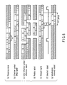
- FIG. 9 shows one transmission symbol of an OFDM. Because a signal component of a guard interval is the same as that of a rear section of an effective symbol, signal components belonging to the guard interval and to the rear section of the effective symbol are indicated, as shown in FIG. 9, as "A" and signal components belonging to other sections are indicated as “B” for simplifying the explanation. To express clearly the fact that the polarities of the signal components indicated by a code A and a code B are inverted with each other, it is defined that the signal components are indicated as "-A" and "-B", respectively. Further, it is defined that the widths of one transmission symbol, of the effective symbol and of the guard interval are indicated as, Ts, Tu and Tg, respectively.
- FIG. 10 is an exemplary view explaining an example of the ISI and the ICI.
- FIG. 10 shows two successive transmission symbols in close-up.
- the addition of a delayed wave (b) of a delay time td (td > Tg) to a desired wave (a) makes the receiver receive a receiving wave (c).
- a conventional receiver cuts out a fast Fourier transform (FFT) period from the receiving wave (c) to perform discrete Fourier transform.
- the cut out FFT period signal (d) seems a signal in which a signal component (e) derived from the same transmission symbol and a signal component (f) derived from the preceding transmission symbol are combined.
- FFT fast Fourier transform
- a continuity of a delay wave component is missing form a section indicated by a dot-line in the signal component (e) derived from the same transmission symbol.
- the missing causes the ICI and further the signal component (f) derived from the preceding transmission causes the ISI.
- the period missing the continuity of the delayed wave component therefrom and the period in which the signal component derived from the preceding transmission exists is the same period during the FFT period. In the present invention, the period in which the signal component of the not desired symbol exists is called "a period subjected to the ISI.”
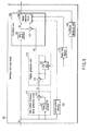
- FIG. 2 is an exemplary block diagram showing a configuration of a receiver for digital modulated signal 20 to which interference removing circuits that will be described in the first embodiment, in a second embodiment and in a third embodiment are applied.
- FIG. 1 is an exemplary block diagram showing a configuration of an interference removing circuit 100 in the first embodiment.
- the first embodiment the following embodiments also go the same
- FIG. 1 shows an example suitable for removing an interference caused by such delayed wave.
- the receiver 20 will be firstly described by referring to FIG. 2.
- a digital complex baseband signal in which a receiving signal is A/D-converted and orthogonally demodulated is input to the receiver 20.
- the removing circuit 100 receives the input digital complex baseband signal and supplies a signal from which the ISI and ICI are removed to an FFT circuit 21.
- the FFT circuit 21 cuts out an FFT period from the signal input in accordance with a symbol synchronous signal generated from a symbol synchronous signal generation unit (not shown) to perform discrete Fourier transform and supplies an obtained baseband signal on a frequency axis to an SP equalizing circuit 22.
- the equalizing circuit 22 waveform-equalizes the signal input having the SP signal included in the input signal as a reference to supply it to a demodulating circuit 23.
- the demodulating circuit 23 demodulates the input signal and reproduces information in the signal obtained in receiving processing to output it as a demodulated output signal.
- the removing circuit 100 comprises a symbol position detector 150 detecting breaks in the transmission symbol from the input signal, a replica generation unit 110 generating a replica signal of a reflected wave from the input signal, a combining unit 140 combining the replica of the reflected wave and the input signal, a coefficient calculation unit 160 estimating the transmission path response from the output of the combining unit 140 to control the property of the replica generation unit 110 and a delay time detector 170 detecting the delay time of the delayed wave from the output of the calculation unit 160.
- the replica generation unit 110 consists of a waveform equalizing unit 120 and a reflected wave component generation unit 130.
- the waveform equalizing unit 120 is composed of an FIR filter 121 which is connected to an output from a subtracter 122 and of which the coefficient is varied by a coefficient calculation unit 160 and the subtracter 122 subtracting the output of the FIR filter 121 from the input signal.
- the component generation unit 130 consists of an FIR filter 131 of which the coefficient is varied by the coefficient calculation unit 160.
- the FIR filter can be composed of, for example, a transversal filter.
- the combining unit 140 includes a symbol position detector 150, a signal cut-out units 141 and 142 each cutting out a part of signals supplied from the replica generation unit 110 on the basis of a detection result from a delay time detector 170, delay circuits 144 and 145 delaying the respective outputs from the cut-out units 141 and 142, a delay circuit 143 delaying the input signal by a prescribed time, and a subtracter 146 and an adder 147 outputting by subtracting and adding the outputs from the delay circuits 144 and 145 from and to the output of the delay circuit 143, respectively.
- the coefficient calculation unit 160 consists of an FFT circuit 161 performing a discrete Fourier transform of the output from the combining 140, a pilot signal extracting unit 162 extracting a pilot signal from the output of the FFT circuit 161, a reference signal generator 163 generating a reference signal equivalent to a pilot signal with not transmission path distortion included therein in synchronization with the extracted pilot signal, a subtracter 164 subtracting the reference signal from the extracted pilot signal, a complex divider 165 diving the output from the subtracter 164 by the reference signal, and an IFFT circuit 166 performing inverse discrete Fourier transform of the subtraction result to output its transform result.
- R( ⁇ ) denotes a frequency characteristic of the known pilot signal inserted by a digital broadcasting transmitting device (not shown)
- S( ⁇ ) denotes a frequency characteristic of the pilot signal included in the receiving signal
- H( ⁇ ) denotes a frequency response of a delayed wave in a transmission path
- the removing circuit 100 operating so as to leave the frequency characteristic of the input signal as it is and remove only the interference component, the coefficient calculation unit 160 receives the frequency characteristic "S( ⁇ )" as it is and the extracting unit 162 can output the "S( ⁇ )".
- the reference signal generator 163 supplies the frequency characteristic "R( ⁇ )" of the known pilot signal then the complex divider 165 outputs "D( ⁇ )" represented by the following equation (2).
- the output "D( ⁇ )" from the complex divider 165 becomes equal to the frequency response "H( ⁇ )" of the delayed wave and the inverse discrete Fourier transform of the output "D( ⁇ )” performed by the IFFT circuit 166 results in an indication of an impulse response of the delayed wave.
- F( ⁇ ) denotes the frequency characteristics of the FIR filter 121, then, the input/output characteristic of the waveform equalizing unit 120 expressed as following equation.
- Z ⁇ Y ⁇ ⁇ F ⁇ ⁇ Z ⁇
- the coefficient of the FIR filter 121 is updated by using the following equation (9).
- C ⁇ k + 1 1 ⁇ ⁇ ⁇ c k + ⁇ ⁇ v k
- v(k) is the output of the coefficient calculation unit 160 of the k-th output (k is positive integer)
- c(k) is the coefficient of the FIR filter 121 and ⁇ is a constant not larger than 1.
- the output from the coefficient calculation unit 160 namely the result from the applying of the inverse discrete Fourier transform by the IFFT circuit 166 is supplied to the delay time detector 170.
- the output from the coefficient calculation unit 160 indicating the impulse response of the delayed wave, for instance, a delay time td of the delayed wave can be obtained from its power peak.
- Delay time information detected by the detector 170 is supplied to the signal cut-out units 141 and 142.
- FIG. 3 is the exemplary view explaining the example of the signal flowing during the operations of the interference removing circuit 100 shown in FIG. 1.
- FIG. 3 shows two successive transmission symbols in close-up.
- the receiving wave (a) to which the delay wave of delay time td (td > Tg) is added to the desired wave is received to be input to the interference removing circuit 100.
- the input receiving wave (a) is input to the symbol position detector 150, the waveform equalizing unit 120 and the combining unit 140.
- the symbol position detector 150 detects the breaks of the symbol of the desired wave to supply the position information to the signal cut-out units 141 and 142.
- a detection method for the breaks of the symbol for instance, utilizing the high correlativity of a part corresponding to the signal parts of the guard interval and the rear part of the effective symbol of the desired wave is a possible approach.
- the equalizing unit 120 equalizes the waveform of the receiving wave (a) on the basis of the filter coefficient supplied from the coefficient calculation unit 160 to supply an equalized signal (b) to the reflected wave component generation unit 130.
- the filter coefficient supplied from the calculation unit 160 being equal to the frequency response "H( ⁇ )" of the delayed wave, giving filter coefficient to the FIR filter 131 and inputting the equalized signal (b) to the FIR filter 131 produces the replica signal of the reflected wave.
- the generation unit 130 supplies a replica signal (c) obtained in such manner to the combining unit 140.
- the receiving wave (a) is input to the delay circuit 143.
- the replica signal (c) is input to the cut-out units 141 and 142.
- the cut-out unit 141 cuts out the period of width Te [partial replica signal 1 (d)] of the part that is the rear end of the transmission symbol preceding the noticed symbol to supply it to the delay circuit 144.
- the width Te denotes the width of the period in which the receiving wave (a) has been affected by the ISI.
- the cut-out unit 142 cuts out the width Te [partial replica signal 2 (e)] of which the rear end is apart from the rear end of the symbol away by Tg from the rear end of the noticed transmission symbol to supply it to the delay circuit 145.
- the partial replica signal 1 (d) obtained in such manner is the replica equivalent to the signal component (f) derived from the preceding transmission symbol described in FIG. 10.
- the partial replica signal 2 (e) is the replica equivalent to the part in which the continuity of the delay wave component described in FIG. 10 has been missed therefrom. Thereby, the combining the receiving wave (a) and these partial replica signals enables removing the ISI and ICI during the FFT period.
- the delay circuits 143, 144 and 145 delay the respective input signals by prescribed time periods to conform the delay of the signals, the subtracter 146 subtracts the partial replica signal 1 (d) from the part that is the head of the FFT period of the noticed transmission symbol of the receiving wave (a), and further, the adder 147 adds the partial replica signal 2 (e) to the part that is the head of the FFT period of the noticed transmission symbol. Then, the combining unit 140 outputs the interference removed output (f) in which the ICI component and the ISI component during the FFT period have been removed from the receiving wave (a) (FFT period is shown in close-up in FIG. 3) is obtained. And the interference removed output (f) is supplied as the output from the FFT circuit 161 and the interference removing circuit 100 to the FFT circuit 21 shown in FIG. 2.
- the combining unit 140 operates to combine a part of the replica signal (c) of the reflected wave in order to remove the ISI and the ICI from the period subjected to the ISI in the receiving wave (a) and to output the receiving wave (a) as it is during a period in which any combination is not performed.
- the affection is restrained in the period with the combination applied therein. So that a new interference is not generated in the period with any combination not performed therein, although the interference is not perfectly removed in the period with the combination applied therein because of errors, but the interference component is reduced, and then, the reception performance is improved as a whole.
- the interference removing circuit 100 operates to reduce the interference while maintaining the transmission path response of the receiving wave (a), the interference removing circuit 100 has advantages such that it can calculate reliability of the demodulation result from a transmission path characteristic appeared in a frequency region after performing FFT and it can apply the conventional technique, as it is, to improve the reception characteristic owing to calculating the reliability.
- the period of the width Te may be determined on the basis of the delay wave with a maximum delay time.
- the period for the combination is not limited to the width Te described above.
- FIG. 4 including the same receiving wave (a), equalized signal (b) and replica signal (c) as those in FIG. 3, the explanation about them will be omitted.
- the partial replica signal 1 (d) in FIG. 4 indicates an aspect to cut out the period including the period of the width Te that is the rear end of the preceding transmission symbol of the notable transmission symbol and expanding the width Te toward the rear and the front by the width Tg from the replica signal (c) of the reflected wave.
- the partial replica signal 2 (e) in FIG. 4 indicates an aspect to cut out the period including the period of the width Te having the part away from the rear end of the notable transmission symbol by the width Tg as a rear end and expanding the width Te toward the rear and the forward by the width Tg from the replica signal (c) of the reflected wave.
- the removing circuit 100 can remove the ICI and the ISI from the FFT period as show by the interference removed output (f). Extending the period for combining up to the end of the transmission symbol produces a possibility to set any part in the transmission symbol as the FFT period and also produces an advantage over obtaining the effect of the present invention. Furthermore, not shown in FIG.
- the front end and the read end of the transmission symbol in the interference removing output (f) become to have identical characteristics, so that S/N improvement effect can be expected by the way to include the signal, in which the period of the width Tg of the front end and the period of the width Tg of the rear end are averaged, to the FFT period.
- the first embodiment has an advantage over increasing the degree of freedom in design. For instance, if it is acceptable that the delay time of the corresponding delayed wave is not longer than 2 X Tg, the removing circuit 100 may generate to combine the partial replica signal 1 (d) and the partial replica signal 2 (e) corresponding to the period of width Tg from the head of the FFT. So that, the removing circuit 100 can be designed to make the width of the period to cut out constant. In this case, not becoming necessary to detect the delay time td, the removing circuit 100 has an advantage of eliminating the delay time detection circuit 170.
- the present invention is not limited to the aforementioned first embodiment.
- a variety of types of modifications based on the first embodiment in accordance with the sprit of the invention can be easily designed, and such case also provides the same effect certainly.
- the replica generation unit 110 is, for example, not always needed to be configured by diving into a wave equalizing unit 120 and the reflected wave component generation unit 130, the FIR filter 121 and FIR filter 131 having been described as different constituent elements so as to facilitate to understand in the first embodiment, the generation unit 110 may combine the two FIR filters 121 and 131 into one FIR filter by utilizing the fact that the two FIR filters receive the same signal and may have the same characteristic.
- the combining unit 140 is configured in such a circuit, for instance, not to perform combining after cutting out the replica signal in advance but appropriately select to output the combination result in which the receiving signal and the replica signal have already being combined over the whole period.
- the estimation method for the transmission path described in this embodiment is one example and other estimation method is available.
- the present invention is also carried out by using a feedfoward-type one. The use of the feedfoward-type one produces the possibility of application of the present invention also to the case for removing the ISI caused by the reflected wave reaches earlier than the desired wave.
- the estimation method described in the embodiment is just one example, and undoubtedly, the other estimation method for the transmission path is useful.
- An algorithm to directly calculate a property of an adaptive filter, as expressed in equation (2), is called a direct analysis-type algorithm for a successive correction-type algorithm such as a least square error method.
- the removing circuit 100 can define the error by means of the waveform equalizing unit 120 to employ the successive correction-type algorithm such as a least square error method. It is just a design matter to determine the type of the algorithm for adoption in implementing the present invention; however, it is no wonder that the direct analysis-type algorithm generally has an advantage of achieving high-speed follow-up to variations in the transmission path response more easily than the successive correction-type algorithm.
- the first embodiment can take a variety of variations also in the generation method and the combining method for the replica signal. And even such methods can certainly extract effective results from the present invention.
- the second embodiment is featured by firstly obtaining the difference between a signal resulting from delaying the receiving wave by the effective symbol period and the receiving wave, then, generates the replica signal on the basis of the difference signal.
- the case in which the interference removing circuit of the second embodiment appropriately selects the result of combination of the receiving wave and the replica signal over the whole period and the receiving wave to output it is also exemplified.
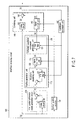
- FIG. 5 is the block diagram showing the configuration of the interference removing circuit in the second embodiment.
- the removing circuit is applied to the receiver for the digital modulated signal 20.
- the removing circuit 100 comprises the symbol position detector 150 detecting breaks in the transmission symbol from the input signal, a inter-symbol difference signal generation circuit 570 outputting the difference between the input signal and the signal resulting from delaying the input signal by the effective symbol period (inter-symbol difference signal), a replica generation unit 510 generating the replica signal of the reflected wave from the inter-symbol difference signal, a combining unit 540 combining the replica signal of the reflected wave and the input signal, the coefficient calculation unit 160 estimating a transmission path response from the output of the combining unit 540 to control a characteristic of the replica generation unit 510 and the delay time detection unit 170 detecting a delay time of a delay wave from the output of the calculation unit 160.
- the difference signal generation circuit 570 consists of a delay circuit 571 delaying the input signal by the effective symbol period and a subtracter 572 subtracting the delay signal from the input signal.
- the replica generation unit 510 is composed of an FIR filter 511 to which the output from a subtracter 512 is connected and of which the coefficient is varied by the calculation unit 160 and the subtracter 512 subtracting the output of the FIR filter 511 from the input signal.
- the combining unit 540 is composed of a delay circuit 541 delaying the input signal by a prescribed time, an adder 542 adding a signal supplied from the replica generation unit 510 to the output from the delay circuit 541 and a signal selection circuit 543 selectively outputs the output from the delay circuit 541 and the output from the adder 542, based on the detection result of the symbol position detector 150 and the delay time detector 170.
- symbol position detector 150 coefficient calculation unit 160 and delay time detector 170 may each have the same configuration and operation as the constituent elements attached the same cords shown in FIG. 1, individual explanations for them will be omitted.
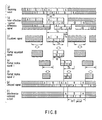
- FIG. 6 shows the exemplary view explaining one example of the signal flowing during the operations of the removing circuit 100 shown in FIG. 5.
- FIG. 6 shows sequencing two transmission symbols in close-up.
- the receiving wave (a) in which the delay wave of delay time td (td > Tg) is added to the desired wave is received to input to the interference removing circuit 100.
- the input receiving wave (a) is input to the symbol position detector 150, the inter-symbol difference signal generation circuit 570 and the combining unit 540.
- the symbol position detector 150 detects the breaks of the desired symbol from the input receiving wave (a) to supply its position information to the signal selection circuit 543.
- the signal generation circuit 570 delays the receiving wave (a) by the time period equivalent to the effective symbol period (period removing the guard interval from the transmission symbol) [(effective symbol delay signal (b)] by means of the delay circuit 571. Then, subtracts the effective symbol delay signal (b) from the input signal through the subtracter 572, and supplies an inter-effective-symbol signal (c) to the replica generation unit 510.
- the guard interval period of the desired wave included in the effective symbol delay signal (b) temporarily coincides with the rear section of the effective symbol having the same signal component as the guard interval of the receiving wave (a), so that the signal components are removed.
- the delay wave goes the same. In showing in a figure, signal components which have cancelled with each other like the inter-effective-symbol difference signal (c) is expressed so as to leave a gap.
- the replica generation unit 510 is an example expressing the replica generation unit 110, described in the first embodiment, by a signal FIR filter and can generate a replica signal (d) of the difference signal from the difference signal (c) to supply it to the combining unit 540 by providing a filter efficient supplied from the calculation unit 160 to the FIR filter 511.
- the replica signal (d) of the difference signal is taken out as an output from the FIR filter 511.
- the generated replica signal (d) of the difference signal is a signal equivalent to a delayed wave component included in the difference signal (c).
- the receiving wave (a) is input to the delay circuit 541.
- the delay circuit 541 delays the receiving wave (a) by the time corresponding to the effective symbol period [delayed signal (e)].
- the adder 542 adds a delayed signal (e) to the replica signal (d) of the difference signal to supply the addition result to the signal selection circuit 543.
- the selection circuit 543 operates so as to selectively output a signal from the adder 542 on the basis of the symbol position information and delay time information during the period of the width Te from the front end of the FFT period and also output the signal from the delay circuit 541 during the period other than the period of the width Te.
- the aspect of the selection can be represented like a selection signal (f).
- the width Te is defined as a width of a period in which the receiving wave (a) is subjected to the ISI.
- the combining unit 540 outputs a result from combing the replica signal (d) of the difference signal in order to remove the ISI and ICI from the receiving wave (a) for the period in which the receiving wave (a) has being subjected to the ISI and operates in order to output the receiving wave (a) as it is for a period other than the above-described period. Even if the foregoing operation occurs an estimation error in estimation of the transmission path response due to temporal variations in noise and the transmission path response and occurs an error in the replica signal (d) of the difference signal, because influence is limited in a period in which the combination has been performed, a new interference is not generated in a period in which the combination has not been performed.
- the period outputting the combination result is not limited to the above-mentioned width Te, and it is needless to say that outputting of the combination result while having a margin by the width Tg at a maximum rear and front sections like the description for the first embodiment produces the same effect.
- the delay circuits 571 and 541 may be configured in a signal delay circuit by aiming that identical signals are input to the two delay circuits 571 and 541 and may each have identical delay times.
- the third embodiment is featured by setting a signal cut-out unit in front of a reflected wave component generation unit. Such a configuration enables the delay time detection circuit to be omitted.
- FIG. 7 is the block diagram showing the configuration of the interference removing circuit 100 in the third embodiment.
- the removing circuit 100 is applied to the receiver for the digital modulated signal 20 shown in FIG. 2.
- the removing circuit 100 comprises the symbol position detector 150 detecting the breaks of the transmission symbol from the input signal, an inter-symbol difference generation circuit 570 outputting the difference (inter-symbol difference signal) between the input signal and a signal resulting from delaying the input signal by the time of the effective symbol period, a replica generation unit 710 generating a partial replica signal of a reflected wave from the inter-symbol difference signal, a combining unit 740 combining the partial replica signal of the reflected wave with the input signal and the coefficient calculation unit 160 estimating the transmission path response from the output of the combining unit 740 to control the property of the replica generation unit 710.
- the replica generation unit 710 is composed of the waveform equalizing unit 120 waveform-equalizing the input inter-symbol difference signal, a signal cut-out unit 711 cutting out a part of the output signal from the equalizing unit 120 and the reflected wave component generation unit 130 generating to output a partial replica signal of the reflected wave from the output of the cut-out unit 711.
- symbol position detector 150 inter-symbol difference signal generation circuit 570, waveform equalizing unit 120, reflected wave component generation unit 130 and coefficient calculation unit 160 may each have the same configuration and operation as the constituent elements with the identical codes shown in FIG. 1 of the first embodiment or shown in FIG. 5 of the second embodiment attached thereto, detailed explanation will be omitted.
- FIG. 8 is the view explaining one example of the signal flowing in operating the interference removing circuit 100 shown in FIG. 7.
- FIG. 8 shows consecutive two transmission symbols in close-up.
- the receiving wave (a) in which the delay wave having the delay time td (td > Tg) is added to the desired wave is received and input to the interference removing circuit 100.
- the input receiving wave (a) is input to the symbol position detector 150, combining unit 570, and combining unit 740.
- the position detector 150 detects the breaks of the desired wave from the input receiving wave (a) to supply the position information to the signal cut-out unit 711 and the signal cut-out unit 742.
- the inter-symbol signal generation circuit 570 generates the effective inter-symbol difference signal (b) from the receiving wave (a) to supply it to the replica generation unit 710.
- the difference signal (b) supplied to the generation unit 710 is input to the waveform equalizing unit 120, and the equalizing unit 120 waveform-equalizes the difference signal (b) on the basis of the filter coefficient supplied from the coefficient calculation unit 160 to supply the equalized signal (c) to the cut-out unit 711.
- the cut-out unit 711 supplies the signal [partial equalized signal (d)] which has been cut out the period of the width Ta from the equalized signal (c) on the basis of the position information of the transmission symbol to the reflected wave component generation unit 130. It is appropriate for the period of the width Ta to be, for instance, a width of Ts/2 by setting a part away from the rear end of the notable transmission symbol by Tg as rear end. In this case, the cut-out unit 711 can produce an effective result to the reflected wave having the delay time not longer than Ts/2.
- the reflected wave component generation unit 130 generates a partial replica signal 1 (e) from the partial equalized signal (d) to supply it to the combining unit 740 by putting the filter coefficient supplied from the coefficient calculation unit 160 to the FIR filter 131.
- the receiving wave (a) is input to the delay circuit 741, and the delay circuit 741 supplies a signal [delayed signal (g)] resulting from delaying the receiving wave (a) by the time equal to the effective symbol period to the adder 743.
- the partial replica signal 1 (e) is input to the cut-out unit 742, and the cut-out unit 742 supplies a signal [partial replica signal 2(f)] by which a period of a width Tb is cut out from the partial replica signal 1 (e) of the reflected wave on the basis of the position information of the transmission symbol.
- the period of the width Tb is suitable, for example, for a period equivalent to the period of the width Ts/2 from the head of the transmission symbol with the delayed signal (g) corresponded thereto.
- the adder 743 adds the input delayed signal (g) to the partial replica signal 2 (f).
- an interference removed output (h) in which the ICI component and the ISI component are removed from the receiving wave (a) is obtained as the output from the combining unit 740 to supply, as the output from the interference removing circuit 100, to the FFT circuit 21 shown in FIG. 2.
- the combining unit 740 operates so that it combines the partial replica signal 1 (e) in the period including a period in which the receiving wave (a) is subjected to the ISI, outputs the result of removing the ISI and ICI, and outputs the receiving wave (a) as it is in the period other than the period including the period.
- the delay circuits 571 and 741 may be configured in a signal delay circuit by aiming that identical signals are input to the two delay circuits 571 and 741 and may each have identical delay times.
- each interference removing circuit receives the receiving wave with the delayed wave of the delay time td (td > Tg) added thereto so as to be described easily
- the present invention is not limited to such a case in which the removing circuit receives a delayed wave of the length exceeding the guard interval length.
- the FFT period receives the ISI resulted from the delay wave of the delay time td (td > Tg/2) and that the applying of the present invention has an effect on such ISI.
- the third embodiment is possible to operate so as to be effective against the reflected wave of the delay time td (Ts/2 > td > 0).
- using the feedforward-type waveform equalizing unit by applying the present invention has an effect also on the case in which the ISI caused by a reflected wave having an arrival time faster than that of a desired wave is expected to remove. Moreover, not being needed to pay an attention to the guard interval length, it is easy to understand that even when receiving an OFDM modulated signal without having the guard interval, the present invention is applicable and effective.
- the present invention is not limited to a receiver for receiving an OFDM modulated signal, and applicable to a receiver for receiving other type of a multi-carrier modulated signal.
- the present invention can be applied to a receiver for digital modulated signal for converting a signal obtained by receiving the multi-carrier modulated signal from a time region into a frequency region by Fourier transform.
- it is suitable for combining the interference removed components generated from the receiving signal on the basis of the transmission path response of the receiving signal with the receiving signal only within a partial period including a period subjected to the ISI among periods to be applied Fourier transform before applying Fourier transform and for doing nothing in the period other than such partial period.
- Such processing is certainly implemented in software processing without using any dedicated hardware and possible to obtain an effect of the present invention similarly.
- the present invention is exemplified in the following aspects.
- the ISI and ICI can be removed by removing interferences in the time region before performing Fourier transform and reception performance is improved.
- the receiver for the digital modulated signal or the receiving method for the same can be provided, respectively.
- the transmission path response of the receiving signal being maintained, the receiver or the receiving method has an advantage such that the conventional technology which can calculate the reliability of the demodulation result from a transmission property appeared in the frequency region after performing Fourier transform and improves the reception property is applicable as it is.
- the transmission path response of the receiving signal being maintained, the receiver or the receiving method has an advantage that the conventional technology which can calculate the reliability of the demodulation result from a transmission property appeared in the frequency region after performing Fourier transform and improves the reception property are applicable as it is.
- the receiver or the receiving method has an advantage that it follows to variations in transmission path response at a high speed easier than a successive correction-type algorithm, by using the direct analysis-type algorithm.
Abstract
Description
- The present invention relates to a receiver for a digital modulated signal and a receiving method for the same, which receives a muti-carrier modulated signal extremely reduced in an inter-symbol interference (hereinafter referred to as ISI) or in an inter-carrier interference (hereinafter referred to as ICI).
- In recent years, a digital modulation method has been widely developed in a transmission of a sound signal and a video signal. In particular, a multi-carrier modulation method has attracted attention in the fact that it has a high resistance to a multi-path interference because it can expand its symbol period length. And then, an orthogonal frequency division multiplexing (OFDM) method and a modulation method derived therefrom have been actively studied.
- Examples of use of OFDM include a terrestrial digital broadcasting. The OFDM is employed for the terrestrial digital broadcasting in Europe and in Japan, because of highly rating the features such that the OFDM has a high resistance to a multi-path interference and high frequency use efficiency. The OFDM is a method for modulating a plurality of carries crossing at right angles with one another by digital data to be transmitted and transmits the digital data by multiplexing those modulated waves. If the number of the carriers to be used is increased to an extent from several-hundred to several-thousand, a width of one symbol becomes extremely wide, so that the OFDM has a feature that it is hardly affected by the muti-path interference. Further, forming a transmission symbol by adding a replica of a signal at a rear section of an effective symbol in front thereof as a guard interval signal, the OFDM becomes possible to disregard the influence of the interference against a multi-path of a delay time not longer than a guard interval length. However, the existence of a multi-path interference of a delay time longer than the guard interval length causes the ISI and the ICI to deteriorate reception performance. The multi-path interference having such a long delay time presents a big problem in implementing a single frequency network (SFN).
- As for a method to solve the problem, a method for canceling the muti-path interference by estimating a transmission path response by use of an adaptive equalizing filter to control a filter coefficient of the adaptive equalizing filter so as to cancel multi-path components has been designed (for instance,
Jpn. Pat. Appln. KOKAI Publications No. 11-298434 No. 2001-292120 - The present invention provides a receiver for a digital modulated signal and a method for the same, which can reduce the ISI or the ICI and improve the reception performance.
- A receiver for a digital modulated signal, which receives a multi-carrier modulated signal and converts a receiving signal from a time region into a frequency region by Fourier transform to demodulate it according to a first aspect of the present invention comprises: a Fourier transformer performing Fourier transform of the receiving signal; and an interference removing circuit disposed at a font stage from the Fourier transformer to reduce an ISI and an ICI of the receiving signal.
- A receiver for a digital modulated signal, which receives a multi-carrier modulated signal and converts a receiving signal from a time region into a frequency region by Fourier transform to demodulate it according to a second aspect of the present invention comprises: a Fourier transformer performing Fourier transform to the receiving signal; and an interference removing circuit disposed at a front stage from the Fourier transformer to reduce an ISI and an ICI of the receiving signal, wherein the removing circuit combines the interference removing components generated from the receiving signal on the basis of a transmission path response only during an appropriate period including a period being interfered from the ISI or the ICI at every period performing Fourier transform and outputs the receiving signal as it is during a period other than the appropriated period.
- A receiving method for a digital modulated signal, which receives a multi-carrier modulated signal and converts a receiving signal from a time region into a frequency region by Fourier transform to demodulate it according to a third aspect of the present invention comprises: reducing an ISI or an ICI of the receiving signal; and performing Fourier transform to the receiving signal in which the interference is reduced.
- This summary of the invention does not necessarily describe all necessary features so that the invention may also be a sub-combination of these described features.
- The invention can be more fully understood from the following detailed description when taken in conjunction with the accompanying drawings, in which:
- FIG. 1 is an exemplary block diagram showing an example of a configuration of an interference removing circuit of a first embodiment that is an embodiment of the present invention;
- FIG. 2 is an exemplary block diagram showing an example of a configuration of a receiver for receiving a digital modulated signal with each of interference removing circuits in a first, a second and a third embodiments that are embodiments of the present invention applied thereto;
- FIG. 3 is an exemplary view explaining an example of a signal flowing during operations of the removing circuit of the first embodiment;
- FIG. 4 is another exemplary view explaining an example of a signal flowing during operations of the removing circuit of the first embodiment;
- FIG. 5 is an exemplary block diagram showing an example of a configuration of an interference removing circuit of a second embodiment that is an example of the present invention;
- FIG. 6 is an exemplary view explaining an example of a signal flowing during operations of the removing circuit of the second embodiment;
- FIG. 7 is an exemplary block diagram showing an example of a configuration of an interference removing circuit of a third embodiment that is an embodiment of the present invention;
- FIG. 8 is an exemplary view explaining an example of a signal flowing during operations of the removing circuit of the third embodiment;
- FIG. 9 is an exemplary view explaining one transmission symbol of OFDM to explain the first embodiment; and
- FIG. 10 is a view explaining an example of an ISI and an ICI to explain the first embodiment.
- The present invention in relation to a receiver for a digital modulated signal, which receives a multi-carrier modulated signal and converts a receiving signal from a time region into a frequency region by Fourier transform to demodulate, is characterized in that the receiver comprises a Fourier transformer performing Fourier transform to the receiving signal, and an interference removing circuit disposed at a front stage from the Fourier transformer to reduce an ISI and an ICI of the receiving signal, wherein the removing circuit combines the interference removing components generated from the receiving signal on the basis of a transmission path response only during an appropriate period including a period being interfered from ISIs or ICIs at every period performing Fourier transform and outputs the receiving signal as it is during a period other than the appropriate period.
- Hereinafter, embodiments of the present invention will be described with reference to embodiments.
- Referring to FIG. 1 to FIG. 4, FIG. 9 and FIG. 10, a first embodiment will be described.
- A first embodiment relates to an Integrated services digital broadcasting for terrestrial (ISDB-T) (other embodiments go the same). In the following explanations, it is presumed that a scattered pilot (hereinafter referred to as SP) carrier that is an amplitude/phase reference is used as a reference signal in estimating a transmission path response.
- The ISI and the ICI will be explained by referring to FIG. 9 and FIG. 10. FIG. 9 shows one transmission symbol of an OFDM. Because a signal component of a guard interval is the same as that of a rear section of an effective symbol, signal components belonging to the guard interval and to the rear section of the effective symbol are indicated, as shown in FIG. 9, as "A" and signal components belonging to other sections are indicated as "B" for simplifying the explanation. To express clearly the fact that the polarities of the signal components indicated by a code A and a code B are inverted with each other, it is defined that the signal components are indicated as "-A" and "-B", respectively. Further, it is defined that the widths of one transmission symbol, of the effective symbol and of the guard interval are indicated as, Ts, Tu and Tg, respectively.
- FIG. 10 is an exemplary view explaining an example of the ISI and the ICI. FIG. 10 shows two successive transmission symbols in close-up. The addition of a delayed wave (b) of a delay time td (td > Tg) to a desired wave (a) makes the receiver receive a receiving wave (c). A conventional receiver cuts out a fast Fourier transform (FFT) period from the receiving wave (c) to perform discrete Fourier transform. The cut out FFT period signal (d) seems a signal in which a signal component (e) derived from the same transmission symbol and a signal component (f) derived from the preceding transmission symbol are combined. As being cleared from FIG. 10, a continuity of a delay wave component is missing form a section indicated by a dot-line in the signal component (e) derived from the same transmission symbol. The missing causes the ICI and further the signal component (f) derived from the preceding transmission causes the ISI. The period missing the continuity of the delayed wave component therefrom and the period in which the signal component derived from the preceding transmission exists is the same period during the FFT period. In the present invention, the period in which the signal component of the not desired symbol exists is called "a period subjected to the ISI."
- FIG. 2 is an exemplary block diagram showing a configuration of a receiver for digital modulated signal 20 to which interference removing circuits that will be described in the first embodiment, in a second embodiment and in a third embodiment are applied. FIG. 1 is an exemplary block diagram showing a configuration of an
interference removing circuit 100 in the first embodiment. To be easily understood, in the first embodiment (the following embodiments also go the same), unless a previous notice is made, the case where a signal in which a delayed wave of one wave having a delay time exceeding a guard interval is added to a desired wave has been receiving will be explained as an example. FIG. 1 shows an example suitable for removing an interference caused by such delayed wave. - The receiver 20 will be firstly described by referring to FIG. 2. A digital complex baseband signal in which a receiving signal is A/D-converted and orthogonally demodulated is input to the receiver 20. The removing
circuit 100 receives the input digital complex baseband signal and supplies a signal from which the ISI and ICI are removed to anFFT circuit 21. TheFFT circuit 21 cuts out an FFT period from the signal input in accordance with a symbol synchronous signal generated from a symbol synchronous signal generation unit (not shown) to perform discrete Fourier transform and supplies an obtained baseband signal on a frequency axis to an SP equalizingcircuit 22. The equalizingcircuit 22 waveform-equalizes the signal input having the SP signal included in the input signal as a reference to supply it to ademodulating circuit 23. Thedemodulating circuit 23 demodulates the input signal and reproduces information in the signal obtained in receiving processing to output it as a demodulated output signal. - Next to this, the
interference removing circuit 100 in the first embodiment will be explained by referring to FIG. 1. The removingcircuit 100 comprises asymbol position detector 150 detecting breaks in the transmission symbol from the input signal, areplica generation unit 110 generating a replica signal of a reflected wave from the input signal, a combiningunit 140 combining the replica of the reflected wave and the input signal, acoefficient calculation unit 160 estimating the transmission path response from the output of the combiningunit 140 to control the property of thereplica generation unit 110 and adelay time detector 170 detecting the delay time of the delayed wave from the output of thecalculation unit 160. - The
replica generation unit 110 consists of awaveform equalizing unit 120 and a reflected wavecomponent generation unit 130. Thewaveform equalizing unit 120 is composed of anFIR filter 121 which is connected to an output from asubtracter 122 and of which the coefficient is varied by acoefficient calculation unit 160 and thesubtracter 122 subtracting the output of theFIR filter 121 from the input signal. Thecomponent generation unit 130 consists of anFIR filter 131 of which the coefficient is varied by thecoefficient calculation unit 160. The FIR filter can be composed of, for example, a transversal filter. - The combining
unit 140 includes asymbol position detector 150, a signal cut-outunits replica generation unit 110 on the basis of a detection result from adelay time detector 170,delay circuits units delay circuit 143 delaying the input signal by a prescribed time, and asubtracter 146 and anadder 147 outputting by subtracting and adding the outputs from thedelay circuits delay circuit 143, respectively. - The
coefficient calculation unit 160 consists of anFFT circuit 161 performing a discrete Fourier transform of the output from the combining 140, a pilotsignal extracting unit 162 extracting a pilot signal from the output of theFFT circuit 161, areference signal generator 163 generating a reference signal equivalent to a pilot signal with not transmission path distortion included therein in synchronization with the extracted pilot signal, asubtracter 164 subtracting the reference signal from the extracted pilot signal, acomplex divider 165 diving the output from thesubtracter 164 by the reference signal, and anIFFT circuit 166 performing inverse discrete Fourier transform of the subtraction result to output its transform result. - Next, operations of the
coefficient calculation unit 160 and thedelay time detector 170 will be explained while explaining the way of thinking for estimation of the transmission path response. - "R(ω)" denotes a frequency characteristic of the known pilot signal inserted by a digital broadcasting transmitting device (not shown), "S(ω)" denotes a frequency characteristic of the pilot signal included in the receiving signal, and "H(ω)" denotes a frequency response of a delayed wave in a transmission path, then, the pilot signal included in the receiving signal is expressed by the following equation (1) and input to the
interference removing circuit 100.
- The removing
circuit 100 operating so as to leave the frequency characteristic of the input signal as it is and remove only the interference component, thecoefficient calculation unit 160 receives the frequency characteristic "S(ω)" as it is and the extractingunit 162 can output the "S(ω)". - Here, the
reference signal generator 163 supplies the frequency characteristic "R(ω)" of the known pilot signal then thecomplex divider 165 outputs "D(ω)" represented by the following equation (2).
- Here, if equation (1) is substituted to the equation (2), the following equation (3) is obtained.

- That is to say, the output "D(ω)" from the
complex divider 165 becomes equal to the frequency response "H(ω)" of the delayed wave and the inverse discrete Fourier transform of the output "D(ω)" performed by theIFFT circuit 166 results in an indication of an impulse response of the delayed wave. - Where "X(ω)" denotes the frequency characteristic of the transmission signal from the digital broadcasting transmitting device, and "Y(ω)" denotes the frequency characteristic of the receiving signal, then, the "Y(ω)" is represented as follows:

- And this output "Y(ω)" is supplied to the
waveform equalizing unit 120 in FIG. 1. Its output is denoted as "Z(ω)". - "F(ω)" denotes the frequency characteristics of the
FIR filter 121, then, the input/output characteristic of thewaveform equalizing unit 120 expressed as following equation.
- Then, the following equation (6) is represented by modifying the equation (5).

- Substituting formula (4) to the equation (6), the following formula (7) is obtained.

- Then, the relationship between the transmitting signal "X(ω)" and the output "Z(ω)" from the
waveform equalizing unit 120 is expressed. - Here, when the result of applying, by the
IFFT circuit 166, inverse discrete Fourier transform to the output "D(ω)" from thecomplex divider 165 is given as the coefficient of theFIR filter 121, namely is set as F(ω) = D(ω), formula (7) is modified as follows:
- Furthermore, substituting formula (3) to formula (8), the following formula is obtained.

- In other words, it becomes possible for the transmitting signal "X(ω)" to be obtained at the output of the
waveform equalizing unit 120 by the above-mentioned operations. - In a state where the
interference removing circuit 100 does not remove an interference or does not remove it sufficiently, the output from the pilotsignal extracting unit 162 possibly includes an error. In this case, the coefficient of theFIR filter 121 is updated by using the following equation (9).
- Where v(k) is the output of the
coefficient calculation unit 160 of the k-th output (k is positive integer), c(k) is the coefficient of theFIR filter 121 and α is a constant not larger than 1. - With repetition of the aforementioned operations, the errors are reduced and the interferences are removed. Setting α as a small value makes the interference removing hardly being affected by noises in the transmission path. In contrast, the temporal variations in the transmission path response requires a large value for the coefficient α.
- The output from the
coefficient calculation unit 160, namely the result from the applying of the inverse discrete Fourier transform by theIFFT circuit 166 is supplied to thedelay time detector 170. As given above, the output from thecoefficient calculation unit 160 indicating the impulse response of the delayed wave, for instance, a delay time td of the delayed wave can be obtained from its power peak. Delay time information detected by thedetector 170 is supplied to the signal cut-outunits - In succession, referring to FIG. 3, the operations of FIG. 1 will be described. FIG. 3 is the exemplary view explaining the example of the signal flowing during the operations of the
interference removing circuit 100 shown in FIG. 1. FIG. 3 shows two successive transmission symbols in close-up. - Firstly, the receiving wave (a) to which the delay wave of delay time td (td > Tg) is added to the desired wave is received to be input to the
interference removing circuit 100. The input receiving wave (a) is input to thesymbol position detector 150, thewaveform equalizing unit 120 and the combiningunit 140. - The
symbol position detector 150 detects the breaks of the symbol of the desired wave to supply the position information to the signal cut-outunits - The equalizing
unit 120 equalizes the waveform of the receiving wave (a) on the basis of the filter coefficient supplied from thecoefficient calculation unit 160 to supply an equalized signal (b) to the reflected wavecomponent generation unit 130. The filter coefficient supplied from thecalculation unit 160 being equal to the frequency response "H(ω)" of the delayed wave, giving filter coefficient to theFIR filter 131 and inputting the equalized signal (b) to theFIR filter 131 produces the replica signal of the reflected wave. Thegeneration unit 130 supplies a replica signal (c) obtained in such manner to the combiningunit 140. - In the combining
unit 140, the receiving wave (a) is input to thedelay circuit 143. The replica signal (c) is input to the cut-outunits unit 141 cuts out the period of width Te [partial replica signal 1 (d)] of the part that is the rear end of the transmission symbol preceding the noticed symbol to supply it to thedelay circuit 144. Here, the width Te denotes the width of the period in which the receiving wave (a) has been affected by the ISI. As shown in FIG. 3, setting the rear part of the transmission symbol to the FFT period, the width Te can be obtained in an equation: Te = td - Tg. The cut-outunit 142 cuts out the width Te [partial replica signal 2 (e)] of which the rear end is apart from the rear end of the symbol away by Tg from the rear end of the noticed transmission symbol to supply it to thedelay circuit 145. The partial replica signal 1 (d) obtained in such manner is the replica equivalent to the signal component (f) derived from the preceding transmission symbol described in FIG. 10. The partial replica signal 2 (e) is the replica equivalent to the part in which the continuity of the delay wave component described in FIG. 10 has been missed therefrom. Thereby, the combining the receiving wave (a) and these partial replica signals enables removing the ISI and ICI during the FFT period. - The
delay circuits subtracter 146 subtracts the partial replica signal 1 (d) from the part that is the head of the FFT period of the noticed transmission symbol of the receiving wave (a), and further, theadder 147 adds the partial replica signal 2 (e) to the part that is the head of the FFT period of the noticed transmission symbol. Then, the combiningunit 140 outputs the interference removed output (f) in which the ICI component and the ISI component during the FFT period have been removed from the receiving wave (a) (FFT period is shown in close-up in FIG. 3) is obtained. And the interference removed output (f) is supplied as the output from theFFT circuit 161 and theinterference removing circuit 100 to theFFT circuit 21 shown in FIG. 2. - That is to say, the combining
unit 140 operates to combine a part of the replica signal (c) of the reflected wave in order to remove the ISI and the ICI from the period subjected to the ISI in the receiving wave (a) and to output the receiving wave (a) as it is during a period in which any combination is not performed. According to such operations, even when an estimation error is made in estimation of a transmission path response due to temporal variations in the noise and the transmission path response to generate an error in the replica signal (c) of the reflected wave, the affection is restrained in the period with the combination applied therein. So that a new interference is not generated in the period with any combination not performed therein, although the interference is not perfectly removed in the period with the combination applied therein because of errors, but the interference component is reduced, and then, the reception performance is improved as a whole. - Operating to reduce the interference while maintaining the transmission path response of the receiving wave (a), the
interference removing circuit 100 has advantages such that it can calculate reliability of the demodulation result from a transmission path characteristic appeared in a frequency region after performing FFT and it can apply the conventional technique, as it is, to improve the reception characteristic owing to calculating the reliability. - In the aforementioned example, having described the delayed wave as one wave, the case in which the receiver is subjected to the ISI caused by a plurality of delayed waves goes the same. In the case of existence of the plurality of delay waves, the period of the width Te may be determined on the basis of the delay wave with a maximum delay time.
- The period for the combination is not limited to the width Te described above.
- Paying attention to the relationship between the replica signal (c) and the interference removing output (f) in FIG. 3 produces easy estimation that a similar effect can be obtained even when the removing
circuit 100 cuts out the partial replica 1 (d) and the partial replica signal 2 (e) with a margin by the width Tg at a maximum at a rear and a front of the transmission symbol for the width Te mentioned above. As an example, the case in which the width Te is cut out wider by the width Tg at the rear and the front of the transmission symbol will be mentioned by referring to FIG. 4. - FIG. 4 including the same receiving wave (a), equalized signal (b) and replica signal (c) as those in FIG. 3, the explanation about them will be omitted. The partial replica signal 1 (d) in FIG. 4 indicates an aspect to cut out the period including the period of the width Te that is the rear end of the preceding transmission symbol of the notable transmission symbol and expanding the width Te toward the rear and the front by the width Tg from the replica signal (c) of the reflected wave. The partial replica signal 2 (e) in FIG. 4 indicates an aspect to cut out the period including the period of the width Te having the part away from the rear end of the notable transmission symbol by the width Tg as a rear end and expanding the width Te toward the rear and the forward by the width Tg from the replica signal (c) of the reflected wave. As cleared by FIG. 4, since the partial replica signal 1 (d) cut out like this and the part indicated by a cord A corresponding to the rear part of the partial replica signal 2 (e) are composed of the same signal components, they are cancelled with each other in combining. Therefore, combining such signal to the receiving wave (a), the removing
circuit 100 can remove the ICI and the ISI from the FFT period as show by the interference removed output (f). Extending the period for combining up to the end of the transmission symbol produces a possibility to set any part in the transmission symbol as the FFT period and also produces an advantage over obtaining the effect of the present invention. Furthermore, not shown in FIG. 3 by omitting, the front end and the read end of the transmission symbol in the interference removing output (f) become to have identical characteristics, so that S/N improvement effect can be expected by the way to include the signal, in which the period of the width Tg of the front end and the period of the width Tg of the rear end are averaged, to the FFT period. - Moreover, extending backward the period for combining is a possible design; the first embodiment has an advantage over increasing the degree of freedom in design. For instance, if it is acceptable that the delay time of the corresponding delayed wave is not longer than 2 X Tg, the removing
circuit 100 may generate to combine the partial replica signal 1 (d) and the partial replica signal 2 (e) corresponding to the period of width Tg from the head of the FFT. So that, the removingcircuit 100 can be designed to make the width of the period to cut out constant. In this case, not becoming necessary to detect the delay time td, the removingcircuit 100 has an advantage of eliminating the delaytime detection circuit 170. - The present invention is not limited to the aforementioned first embodiment. A variety of types of modifications based on the first embodiment in accordance with the sprit of the invention can be easily designed, and such case also provides the same effect certainly. The
replica generation unit 110 is, for example, not always needed to be configured by diving into awave equalizing unit 120 and the reflected wavecomponent generation unit 130, theFIR filter 121 andFIR filter 131 having been described as different constituent elements so as to facilitate to understand in the first embodiment, thegeneration unit 110 may combine the twoFIR filters unit 140 to be configured in such a circuit, for instance, not to perform combining after cutting out the replica signal in advance but appropriately select to output the combination result in which the receiving signal and the replica signal have already being combined over the whole period. The estimation method for the transmission path described in this embodiment is one example and other estimation method is available. Further, having described the embodiment by use of the feedback-type wave equalizing unit, the present invention is also carried out by using a feedfoward-type one. The use of the feedfoward-type one produces the possibility of application of the present invention also to the case for removing the ISI caused by the reflected wave reaches earlier than the desired wave. - The estimation method described in the embodiment is just one example, and undoubtedly, the other estimation method for the transmission path is useful. An algorithm to directly calculate a property of an adaptive filter, as expressed in equation (2), is called a direct analysis-type algorithm for a successive correction-type algorithm such as a least square error method. Not described here, the removing
circuit 100 can define the error by means of thewaveform equalizing unit 120 to employ the successive correction-type algorithm such as a least square error method. It is just a design matter to determine the type of the algorithm for adoption in implementing the present invention; however, it is no wonder that the direct analysis-type algorithm generally has an advantage of achieving high-speed follow-up to variations in the transmission path response more easily than the successive correction-type algorithm. - Moreover, the first embodiment can take a variety of variations also in the generation method and the combining method for the replica signal. And even such methods can certainly extract effective results from the present invention.
- Referring next to FIG. 5 and FIG. 6, a second embodiment will be set forth.
- In particular, another embodiment in which a generation method and a combining method for a replica signal have been changed will be explained. The second embodiment is featured by firstly obtaining the difference between a signal resulting from delaying the receiving wave by the effective symbol period and the receiving wave, then, generates the replica signal on the basis of the difference signal. The case in which the interference removing circuit of the second embodiment appropriately selects the result of combination of the receiving wave and the replica signal over the whole period and the receiving wave to output it is also exemplified.
- FIG. 5 is the block diagram showing the configuration of the interference removing circuit in the second embodiment. The removing circuit is applied to the receiver for the digital modulated signal 20.
- The removing
circuit 100 comprises thesymbol position detector 150 detecting breaks in the transmission symbol from the input signal, a inter-symbol differencesignal generation circuit 570 outputting the difference between the input signal and the signal resulting from delaying the input signal by the effective symbol period (inter-symbol difference signal), areplica generation unit 510 generating the replica signal of the reflected wave from the inter-symbol difference signal, a combiningunit 540 combining the replica signal of the reflected wave and the input signal, thecoefficient calculation unit 160 estimating a transmission path response from the output of the combiningunit 540 to control a characteristic of thereplica generation unit 510 and the delaytime detection unit 170 detecting a delay time of a delay wave from the output of thecalculation unit 160. - The difference
signal generation circuit 570 consists of adelay circuit 571 delaying the input signal by the effective symbol period and asubtracter 572 subtracting the delay signal from the input signal. - The
replica generation unit 510 is composed of anFIR filter 511 to which the output from asubtracter 512 is connected and of which the coefficient is varied by thecalculation unit 160 and thesubtracter 512 subtracting the output of theFIR filter 511 from the input signal. - The combining
unit 540 is composed of adelay circuit 541 delaying the input signal by a prescribed time, anadder 542 adding a signal supplied from thereplica generation unit 510 to the output from thedelay circuit 541 and asignal selection circuit 543 selectively outputs the output from thedelay circuit 541 and the output from theadder 542, based on the detection result of thesymbol position detector 150 and thedelay time detector 170. - Because the
symbol position detector 150,coefficient calculation unit 160 and delaytime detector 170 may each have the same configuration and operation as the constituent elements attached the same cords shown in FIG. 1, individual explanations for them will be omitted. - Successively, the operations of the removing
circuit 100 in FIG. 5 regarding the second embodiment will be described with reference to FIG. 6. FIG. 6 shows the exemplary view explaining one example of the signal flowing during the operations of the removingcircuit 100 shown in FIG. 5. FIG. 6 shows sequencing two transmission symbols in close-up. - Firstly, the receiving wave (a) in which the delay wave of delay time td (td > Tg) is added to the desired wave is received to input to the
interference removing circuit 100. The input receiving wave (a) is input to thesymbol position detector 150, the inter-symbol differencesignal generation circuit 570 and the combiningunit 540. - The
symbol position detector 150 detects the breaks of the desired symbol from the input receiving wave (a) to supply its position information to thesignal selection circuit 543. - The
signal generation circuit 570 delays the receiving wave (a) by the time period equivalent to the effective symbol period (period removing the guard interval from the transmission symbol) [(effective symbol delay signal (b)] by means of thedelay circuit 571. Then, subtracts the effective symbol delay signal (b) from the input signal through thesubtracter 572, and supplies an inter-effective-symbol signal (c) to thereplica generation unit 510. As known from FIG. 6, the guard interval period of the desired wave included in the effective symbol delay signal (b) temporarily coincides with the rear section of the effective symbol having the same signal component as the guard interval of the receiving wave (a), so that the signal components are removed. The delay wave goes the same. In showing in a figure, signal components which have cancelled with each other like the inter-effective-symbol difference signal (c) is expressed so as to leave a gap. - The
replica generation unit 510 is an example expressing thereplica generation unit 110, described in the first embodiment, by a signal FIR filter and can generate a replica signal (d) of the difference signal from the difference signal (c) to supply it to the combiningunit 540 by providing a filter efficient supplied from thecalculation unit 160 to theFIR filter 511. The replica signal (d) of the difference signal is taken out as an output from theFIR filter 511. The generated replica signal (d) of the difference signal is a signal equivalent to a delayed wave component included in the difference signal (c). - In the combining
unit 540, the receiving wave (a) is input to thedelay circuit 541. Thedelay circuit 541 delays the receiving wave (a) by the time corresponding to the effective symbol period [delayed signal (e)]. Theadder 542 adds a delayed signal (e) to the replica signal (d) of the difference signal to supply the addition result to thesignal selection circuit 543. Theselection circuit 543 operates so as to selectively output a signal from theadder 542 on the basis of the symbol position information and delay time information during the period of the width Te from the front end of the FFT period and also output the signal from thedelay circuit 541 during the period other than the period of the width Te. The aspect of the selection can be represented like a selection signal (f). Here, the width Te is defined as a width of a period in which the receiving wave (a) is subjected to the ISI. As shown in FIG. 6, when the rear section of the transmission symbol is defined as the FFT period, the width Te is obtained in an equation: Te = td - Tg. - In other words, the combining
unit 540 outputs a result from combing the replica signal (d) of the difference signal in order to remove the ISI and ICI from the receiving wave (a) for the period in which the receiving wave (a) has being subjected to the ISI and operates in order to output the receiving wave (a) as it is for a period other than the above-described period. Even if the foregoing operation occurs an estimation error in estimation of the transmission path response due to temporal variations in noise and the transmission path response and occurs an error in the replica signal (d) of the difference signal, because influence is limited in a period in which the combination has been performed, a new interference is not generated in a period in which the combination has not been performed. And although the interference cannot be removed completely because of the error in the period in which the combination has been performed, owing to the reduction in the interference component, reception performance is improved. The period outputting the combination result is not limited to the above-mentioned width Te, and it is needless to say that outputting of the combination result while having a margin by the width Tg at a maximum rear and front sections like the description for the first embodiment produces the same effect. - A variety of modifications are easily designed in the second embodiment, and such modifications each have the same effects certainly. For instance, having described that the
delay circuit 571 anddelay circuit 541 as individual constituent elements for easy understanding, thedelay circuits delay circuits - In succession, a third embodiment will be described by referring to FIG. 7 and FIG. 8.
- Other embodiment varying the generation method and combining method for the replica signal will be described. The third embodiment is featured by setting a signal cut-out unit in front of a reflected wave component generation unit. Such a configuration enables the delay time detection circuit to be omitted.
- FIG. 7 is the block diagram showing the configuration of the
interference removing circuit 100 in the third embodiment. The removingcircuit 100 is applied to the receiver for the digital modulated signal 20 shown in FIG. 2. - The removing
circuit 100 comprises thesymbol position detector 150 detecting the breaks of the transmission symbol from the input signal, an inter-symboldifference generation circuit 570 outputting the difference (inter-symbol difference signal) between the input signal and a signal resulting from delaying the input signal by the time of the effective symbol period, areplica generation unit 710 generating a partial replica signal of a reflected wave from the inter-symbol difference signal, a combiningunit 740 combining the partial replica signal of the reflected wave with the input signal and thecoefficient calculation unit 160 estimating the transmission path response from the output of the combiningunit 740 to control the property of thereplica generation unit 710. - The
replica generation unit 710 is composed of thewaveform equalizing unit 120 waveform-equalizing the input inter-symbol difference signal, a signal cut-outunit 711 cutting out a part of the output signal from the equalizingunit 120 and the reflected wavecomponent generation unit 130 generating to output a partial replica signal of the reflected wave from the output of the cut-outunit 711. - A
delay circuit 741 delaying the input signal to a predetermined time, a signal cut-outunit 742 cutting out a part of the partial replica signal of the reflected wave on the basis of the detection result from thedetector 150, and anadder 743 adding to out the output from thedelay circuit 741 and the signal cut-outunit 742 constitute the combiningunit 740. - Because the
symbol position detector 150, inter-symbol differencesignal generation circuit 570,waveform equalizing unit 120, reflected wavecomponent generation unit 130 andcoefficient calculation unit 160 may each have the same configuration and operation as the constituent elements with the identical codes shown in FIG. 1 of the first embodiment or shown in FIG. 5 of the second embodiment attached thereto, detailed explanation will be omitted. - Next to this, operations of FIG. 7 will be set forth by use of FIG. 8. FIG. 8 is the view explaining one example of the signal flowing in operating the
interference removing circuit 100 shown in FIG. 7. FIG. 8 shows consecutive two transmission symbols in close-up. - At first, the receiving wave (a) in which the delay wave having the delay time td (td > Tg) is added to the desired wave is received and input to the
interference removing circuit 100. The input receiving wave (a) is input to thesymbol position detector 150, combiningunit 570, and combiningunit 740. - The
position detector 150 detects the breaks of the desired wave from the input receiving wave (a) to supply the position information to the signal cut-outunit 711 and the signal cut-outunit 742. - The inter-symbol
signal generation circuit 570 generates the effective inter-symbol difference signal (b) from the receiving wave (a) to supply it to thereplica generation unit 710. - The difference signal (b) supplied to the
generation unit 710 is input to thewaveform equalizing unit 120, and the equalizingunit 120 waveform-equalizes the difference signal (b) on the basis of the filter coefficient supplied from thecoefficient calculation unit 160 to supply the equalized signal (c) to the cut-outunit 711. - The cut-out
unit 711 supplies the signal [partial equalized signal (d)] which has been cut out the period of the width Ta from the equalized signal (c) on the basis of the position information of the transmission symbol to the reflected wavecomponent generation unit 130. It is appropriate for the period of the width Ta to be, for instance, a width of Ts/2 by setting a part away from the rear end of the notable transmission symbol by Tg as rear end. In this case, the cut-outunit 711 can produce an effective result to the reflected wave having the delay time not longer than Ts/2. - The reflected wave
component generation unit 130 generates a partial replica signal 1 (e) from the partial equalized signal (d) to supply it to the combiningunit 740 by putting the filter coefficient supplied from thecoefficient calculation unit 160 to theFIR filter 131. - In the combining
unit 740, the receiving wave (a) is input to thedelay circuit 741, and thedelay circuit 741 supplies a signal [delayed signal (g)] resulting from delaying the receiving wave (a) by the time equal to the effective symbol period to theadder 743. The partial replica signal 1 (e) is input to the cut-outunit 742, and the cut-outunit 742 supplies a signal [partial replica signal 2(f)] by which a period of a width Tb is cut out from the partial replica signal 1 (e) of the reflected wave on the basis of the position information of the transmission symbol. The period of the width Tb is suitable, for example, for a period equivalent to the period of the width Ts/2 from the head of the transmission symbol with the delayed signal (g) corresponded thereto. - The
adder 743 adds the input delayed signal (g) to the partial replica signal 2 (f). - As a result, an interference removed output (h) in which the ICI component and the ISI component are removed from the receiving wave (a) is obtained as the output from the combining
unit 740 to supply, as the output from theinterference removing circuit 100, to theFFT circuit 21 shown in FIG. 2. - That is to say, the combining
unit 740 operates so that it combines the partial replica signal 1 (e) in the period including a period in which the receiving wave (a) is subjected to the ISI, outputs the result of removing the ISI and ICI, and outputs the receiving wave (a) as it is in the period other than the period including the period. Even when an estimation error in the estimation of the transmission path response occurs owing to temporal variations in noise and the transmission path response and occurs an error in the partial replica signal 1 (e) of the difference signal, the affection being limited in the period in which the combination has been performed, a new interference does not occur in the period in which the combination has not been performed. Then, although the interference is not removed perfectly due to the error in the period in which the combination has been performed, the interference components are reduced, so that the reception performance is improved. - For the embodiment, a various modifications are easily designed, and even in such modifications, the same effects are certainly produced. For instance, having described that the
delay circuit 571 anddelay circuit 741 as individual constituent elements for easy understanding, thedelay circuits delay circuits - In the first, second and third embodiments, having described the case where each interference removing circuit receives the receiving wave with the delayed wave of the delay time td (td > Tg) added thereto so as to be described easily, the present invention is not limited to such a case in which the removing circuit receives a delayed wave of the length exceeding the guard interval length. For instance, it is easy to understand that when the center of the transmission symbol is determined as the FFT period, the FFT period receives the ISI resulted from the delay wave of the delay time td (td > Tg/2) and that the applying of the present invention has an effect on such ISI. The third embodiment is possible to operate so as to be effective against the reflected wave of the delay time td (Ts/2 > td > 0). Furthermore, as also described in the first embodiment, using the feedforward-type waveform equalizing unit by applying the present invention has an effect also on the case in which the ISI caused by a reflected wave having an arrival time faster than that of a desired wave is expected to remove. Moreover, not being needed to pay an attention to the guard interval length, it is easy to understand that even when receiving an OFDM modulated signal without having the guard interval, the present invention is applicable and effective.
- The present invention is not limited to a receiver for receiving an OFDM modulated signal, and applicable to a receiver for receiving other type of a multi-carrier modulated signal. In view of the aforementioned embodiments, it is easily understood that the present invention can be applied to a receiver for digital modulated signal for converting a signal obtained by receiving the multi-carrier modulated signal from a time region into a frequency region by Fourier transform. In other words, it is suitable for combining the interference removed components generated from the receiving signal on the basis of the transmission path response of the receiving signal with the receiving signal only within a partial period including a period subjected to the ISI among periods to be applied Fourier transform before applying Fourier transform and for doing nothing in the period other than such partial period. Such processing is certainly implemented in software processing without using any dedicated hardware and possible to obtain an effect of the present invention similarly.
- The present invention is exemplified in the following aspects.
- (1) A receiver for a digital modulated signal, which receives a multi-carrier modulated signal and demodulates a receiving signal by converting it from a time region into a frequency region by Fourier transform, comprises a Fourier transformer which performs Fourier transform; and an interference removing circuit which is disposed in a front stage of the Fourier transformer and reduces the ISI or ICI of the receiving signal.
- (2) The receiver described as in (1), wherein the interference moving circuit reduces the interference by applying signal processing to the receiving signal in the time region on the basis of a transmission path response estimated from the receiving signal.
- (3) The receiver described as in either (1) or (2), wherein the interference removing circuit operates so as to reduce the interference while maintaining a transmission path response of the receiving signal.
- (4) A receiver for digital modulated signal, which receives a multi-carrier modulated signal and demodulates a receiving signal by converting it from a time region into a frequency region by Fourier transform, comprises a Fourier transformer which performs Fourier transform; and an interference removing circuit which is disposed in a front stage of the Fourier transformer and reduces ISI or ICI of the receiving signal, wherein the circuit each combines interference removing components generated from the receiving signal with the receiving signal at every period for performing the Fourier transform on the basis of a transmission path response of the receiving signal only in an appropriate period including a period subjected the ISI or ICI and outputs the receiving signal as it is other than the appropriate period.
- (5) The receiver described as in (4), wherein the removing circuit includes a replica generation unit which generates the interference removing component from the receiving signal; a combining unit which combines the interference removing component with the receiving signal; and a coefficient calculation unit which estimates the transmission path response from the receiving signal to control a characteristic of the replica generation unit.
- (6) The receiver described as in (5), wherein the coefficient calculation unit estimates a transmission path response from an output signal of the interference removing circuit
- (7) The receiver described as in any one of (1)-(6), wherein the Fourier transformer performs Fourier transform by fast Fourier transform (FFT).
- (8) The receiver described as in any one of (1)-(7), wherein the multi-carrier modulated signal is an orthogonal frequency division multiplexing (OFDM)-modulated signal.
- (9) The receiver described as in any one of (6)-(8), wherein the transmission path response is estimated by using a direct analysis-type algorithm.
- (10) A receiving method for a digital modulated signal, which receives a multi-carrier modulated signal and demodulates a receiving signal by converting it from a time region into a frequency region by Fourier transform, comprises reducing ISI or ICI on the receiving signal; and performing Fourier transform of the receiving signal reduced in the ISI or the ICI.
- (11) The receiving method described as in (10), wherein the ISI or ICI of the receiving signal is reduced by applying time region processing to the receiving signal on the basis of transmission path response estimated from the receiving signal.
- (12) The receiving method described as in either (10) or (11), wherein the ISI or ICI of the receiving signal is reduced while maintaining a transmission path response of the receiving signal.
- (13) The receiving method described as in (10), further comprise generating an interference removing component from the receiving signal on the basis of a transmission path response of the receiving signal; combining the interference removing component with the receiving signal in an appropriate period including a period subjected to the ISI or the ICI of the receiving signal; and not combining in a period other than the appropriate period.
- (14) The receiving method described as in (13), wherein the transmission path response is estimated from a signal after performing the interference removing.
- (15) The receiving method described as in any one of (10) to (14), wherein the Fourier transform is performed by FFT.
- (16) The receiving method described as in any one of (10) to (15), wherein the multi-carrier modulated signal is an OFDM-modulated signal.
- (17) The receiving method described as in any one of (14) to (16), wherein the transmission path response is estimated by using a direct analysis-type algorithm.
- According to the aforementioned (1), (2) or (10), (11), the ISI and ICI can be removed by removing interferences in the time region before performing Fourier transform and reception performance is improved. As a result, the receiver for the digital modulated signal or the receiving method for the same can be provided, respectively.
- According to the aforementioned (3) or (12), the transmission path response of the receiving signal being maintained, the receiver or the receiving method has an advantage such that the conventional technology which can calculate the reliability of the demodulation result from a transmission property appeared in the frequency region after performing Fourier transform and improves the reception property is applicable as it is.
- According to the foregoing (4) or (13), the transmission path response of the receiving signal being maintained, the receiver or the receiving method has an advantage that the conventional technology which can calculate the reliability of the demodulation result from a transmission property appeared in the frequency region after performing Fourier transform and improves the reception property are applicable as it is.
- According to the above-described (9) or (17), the receiver or the receiving method has an advantage that it follows to variations in transmission path response at a high speed easier than a successive correction-type algorithm, by using the direct analysis-type algorithm.
Claims (17)
- A receiver for digital modulated signal (20), which receives a multi-carrier modulated signal and demodulates a receiving signal by converting it from a time region into a frequency region by Fourier transform, characterized by comprising:a Fourier transformer (21) which performs Fourier transform of the receiving signal; andan interference removing circuit (100) which is disposed in a front stage of the Fourier transformer and reduces an inter-symbol interference or an inter-carrier interference of the receiving signal.
- The receiver according to claim 1, characterized in that the interference moving circuit (100) reduces the interference by applying signal processing to the receiving signal in the time region on the basis of a transmission path response estimated from the receiving signal.
- The receiver according to one of claim 1 and claim 2, characterized in that the interference removing circuit (100) operates so as to reduce the interference while maintaining a transmission path response of the receiving signal.
- A receiver for digital modulated signal (20), which receives a multi-carrier modulated signal and demodulates a receiving signal by converting it from a time region into a frequency region by Fourier transform, characterized by comprising:a Fourier transformer (21) which performs Fourier transform of the receiving signal;and an interference removing circuit (100) which is disposed in a front stage of the Fourier transformer and reduces an inter-symbol interference or an inter-carrier interference of the receiving signal, wherein the removing circuit (100) each combines interference removing component generated from the receiving signal with the receiving signal at every Fourier transform on the basis of a transmission path response of the receiving signal only in an appropriate period including a period subjected to the inter-symbol interference or the inter-carrier interference and outputs the receiving signal as it is other than the appropriate period.
- The receiver according to claim 4, characterized in that the interference removing circuit (100) comprises:a replica generation unit (110) which generates the interference removing component from the receiving signal,a combining unit (140) which combines the interference removing component with the receiving signal, anda coefficient calculation unit (160) which estimates the transmission path response from the receiving signal to control a characteristic of the replica generation unit (110).
- The receiver according to claim 5, characterized in that the coefficient calculation unit (160) estimates a transmission path response from an output signal of the interference removing circuit (100).
- The receiver according to any one of claims 1, 2 and 4 to 6, characterized in that the Fourier transformer (21) performes the Fourier transform by fast Fourier transform (FFT).
- The receiver according to any one of claims 1, 2 and 4 to 6, characterized in that the multi-carrier modulated signal is an orthogonal frequency division multiplexing (OFDM)-modulated signal.
- The receiver according to claim 6, characterized in that the estimation of the transmission path response uses a direct analysis-type algorithm.
- A receiving method for a digital modulated signal, which receives a multi-carrier modulated signal and demodulates a receiving signal by converting it from a time region into a frequency region, characterized by comprising:reducing an inter-symbol interference or an inter-carrier interference of the receiving signal; andperforming Fourier transform of the receiving signal reduced in the inter-symbol interference or the inter-carrier interference.
- The receiving method according to claim 10, characterized in that the inter-symbol interference or the inter-carrier interference of the receiving signal reduces while applying time region processing to the receiving signal on the basis of transmission path response estimated from the receiving signal.
- The receiving method according to one of claim 10 and claim 11, characterized in that the inter-symbol interference or the inter-carrier interference of the receiving signal reduces while maintaining a transmission path response of the receiving signal.
- The receiving method according to claim 10, the inter-symbol interference or the inter-carrier interference of the receiving signal is characterized by comprising:generating an interference removing component from the receiving signal on the basis of a transmission path response of the receiving signal;combining the interference removing component with the receiving signal in an appropriate period including a period subjected to the inter-symbol interference or the inter-carrier interference of the receiving signal; andnot combining the interference removing component in a period other than the appropriate period.
- The receiving method according to claim 13, characterized in that the transmission path response is estimated from a signal after reducing the interference.
- The receiving method according to any one of claims 10, 11, 13 and 14, characterized in that the Fourier transform is performed by FFT.
- The receiving method according to any one of claims 10, 11, 13 and 14, characterized in that the multi-carrier modulated signal is an OFDM-modulated signal.
- The receiving method according to claim 14, characterized in that the transmission path response is estimated by using a direct analysis-type algorithm.
Applications Claiming Priority (1)
| Application Number | Priority Date | Filing Date | Title |
|---|---|---|---|
| JP2005183007A JP5072199B2 (en) | 2005-06-23 | 2005-06-23 | Digital modulation signal receiving apparatus and receiving method thereof |
Publications (2)
| Publication Number | Publication Date |
|---|---|
| EP1737177A2 true EP1737177A2 (en) | 2006-12-27 |
| EP1737177A3 EP1737177A3 (en) | 2013-10-23 |
Family
ID=37075208
Family Applications (1)
| Application Number | Title | Priority Date | Filing Date |
|---|---|---|---|
| EP06013015.0A Withdrawn EP1737177A3 (en) | 2005-06-23 | 2006-06-23 | Receiver for digital modulated signal and receiving method for the same |
Country Status (4)
| Country | Link |
|---|---|
| US (1) | US8345802B2 (en) |
| EP (1) | EP1737177A3 (en) |
| JP (1) | JP5072199B2 (en) |
| CN (1) | CN1885840B (en) |
Cited By (1)
| Publication number | Priority date | Publication date | Assignee | Title |
|---|---|---|---|---|
| US8462900B2 (en) | 2008-02-27 | 2013-06-11 | Panasonic Corporation | Reception device, integrated circuit, and reception method |
Families Citing this family (19)
| Publication number | Priority date | Publication date | Assignee | Title |
|---|---|---|---|---|
| US7844018B2 (en) * | 2007-01-02 | 2010-11-30 | Qualcomm Incorporated | Methods and apparatuses for reducing inter-carrier interference in an OFDM system |
| JP5242924B2 (en) * | 2007-02-26 | 2013-07-24 | Necディスプレイソリューションズ株式会社 | Video display system, video signal transmitter and video display device |
| JP4963723B2 (en) * | 2007-06-19 | 2012-06-27 | シャープ株式会社 | Receiver, receiving method and integrated circuit |
| CN101689954A (en) * | 2007-06-26 | 2010-03-31 | 夏普株式会社 | Receiver and reception method |
| CN101796754A (en) * | 2007-09-05 | 2010-08-04 | 夏普株式会社 | Reception device and reception method |
| US8571136B1 (en) * | 2007-11-21 | 2013-10-29 | University Of South Florida | Adaptive symbol transition method for OFDM-based cognitive radio systems |
| US8139664B2 (en) | 2007-11-28 | 2012-03-20 | Sony Corporation | Reception apparatus, reception method and program |
| JP2009186241A (en) * | 2008-02-04 | 2009-08-20 | Sumitomo Electric Ind Ltd | Receiving device range-finding system, positioning system, computer program, and reception time point determining method |
| KR101138602B1 (en) * | 2008-04-17 | 2012-04-26 | 주식회사 코아로직 | Orthogonal frequency division multiplexingOFDM receiving apparatus and method of minimizing inter symbol interferenceISI using the same the apparatus |
| JP4569695B2 (en) * | 2008-09-19 | 2010-10-27 | ソニー株式会社 | Equalizer, equalization method, program, receiver |
| JP5644475B2 (en) | 2010-02-18 | 2014-12-24 | 富士通株式会社 | Receiver |
| US8655282B2 (en) * | 2010-10-29 | 2014-02-18 | Qualcomm Incorporated | Multiple signal transformation in wireless receivers |
| JP2012204941A (en) * | 2011-03-24 | 2012-10-22 | Toshiba Corp | Receiving device and receiving method |
| US20120295565A1 (en) * | 2011-05-16 | 2012-11-22 | Raytheon Company | System and method for analog interference suppression in pulsed signal processing |
| US8614940B1 (en) | 2012-11-14 | 2013-12-24 | The Aerospace Corporation | Systems and methods for reducing narrow bandwidth interference contained in broad bandwidth signals |
| CN109328434B (en) * | 2016-06-24 | 2021-07-30 | 株式会社索思未来 | Equalizing circuit, receiving circuit and integrated circuit device |
| US9628122B1 (en) | 2016-07-25 | 2017-04-18 | The Aerospace Corporation | Circuits and methods for reducing interference that spectrally overlaps a desired signal based on dynamic gain control and/or equalization |
| US10056675B1 (en) | 2017-08-10 | 2018-08-21 | The Aerospace Corporation | Systems and methods for reducing directional interference based on adaptive excision and beam repositioning |
| US11212015B2 (en) | 2020-05-19 | 2021-12-28 | The Aerospace Corporation | Interference suppression using machine learning |
Family Cites Families (13)
| Publication number | Priority date | Publication date | Assignee | Title |
|---|---|---|---|---|
| JP2934225B1 (en) | 1998-04-06 | 1999-08-16 | 株式会社次世代デジタルテレビジョン放送システム研究所 | OFDM demodulator |
| JP3084368B1 (en) * | 1999-03-30 | 2000-09-04 | 株式会社次世代デジタルテレビジョン放送システム研究所 | OFDM receiver |
| JP4113651B2 (en) * | 2000-04-10 | 2008-07-09 | 日本放送協会 | Digital broadcast receiver |
| US7012968B2 (en) * | 2000-11-30 | 2006-03-14 | Lg Electronics, Inc. | Apparatus for detecting and adjusting transmission power of CDMA system |
| JP2003051802A (en) * | 2001-08-06 | 2003-02-21 | Nippon Hoso Kyokai <Nhk> | Digital reception system |
| CN1488209A (en) | 2001-08-28 | 2004-04-07 | 松下电器产业株式会社 | Multi-pass interference removal apparatus and multi-pass interference removal method |
| US7221958B2 (en) * | 2001-12-12 | 2007-05-22 | Ericsson Inc. | Received signal filtering for enhanced selectivity |
| JP4298320B2 (en) * | 2002-11-08 | 2009-07-15 | 富士通株式会社 | Receiver for OFDM transmission system |
| JP4090331B2 (en) * | 2002-11-20 | 2008-05-28 | 三洋電機株式会社 | Reception method and apparatus |
| US20050002474A1 (en) * | 2003-01-27 | 2005-01-06 | Limberg Allen Leroy | PAM radio signal receiver with phase-tracker succeeding adaptive FIR filtering and preceding adaptive IIR filtering |
| US7209716B2 (en) * | 2003-02-27 | 2007-04-24 | Ntt Docomo, Inc. | Radio communication system, radio station, and radio communication method |
| JP2005260337A (en) * | 2004-03-09 | 2005-09-22 | Renesas Technology Corp | Demodulation circuit and radio communication system |
| JP4421416B2 (en) * | 2004-08-04 | 2010-02-24 | 富士通株式会社 | OFDM receiver |
-
2005
- 2005-06-23 JP JP2005183007A patent/JP5072199B2/en active Active
-
2006
- 2006-06-22 US US11/472,351 patent/US8345802B2/en active Active
- 2006-06-23 CN CN2006100932406A patent/CN1885840B/en active Active
- 2006-06-23 EP EP06013015.0A patent/EP1737177A3/en not_active Withdrawn
Non-Patent Citations (1)
| Title |
|---|
| None * |
Cited By (1)
| Publication number | Priority date | Publication date | Assignee | Title |
|---|---|---|---|---|
| US8462900B2 (en) | 2008-02-27 | 2013-06-11 | Panasonic Corporation | Reception device, integrated circuit, and reception method |
Also Published As
| Publication number | Publication date |
|---|---|
| CN1885840B (en) | 2012-03-21 |
| EP1737177A3 (en) | 2013-10-23 |
| JP2007006067A (en) | 2007-01-11 |
| US20060291375A1 (en) | 2006-12-28 |
| JP5072199B2 (en) | 2012-11-14 |
| CN1885840A (en) | 2006-12-27 |
| US8345802B2 (en) | 2013-01-01 |
Similar Documents
| Publication | Publication Date | Title |
|---|---|---|
| US8345802B2 (en) | Receiver for digital modulated signal and receiving method for the same | |
| EP1746794B1 (en) | Path selection in an OFDM apparatus | |
| JP4961918B2 (en) | OFDM receiving apparatus and OFDM receiving method | |
| EP1523143B1 (en) | Receiving apparatus in OFDM transmission system | |
| JP4523294B2 (en) | Communication device | |
| EP1580948A2 (en) | Receiver | |
| US20040141570A1 (en) | Symbol timing correction circuit, receiver, symbol timing correction, mothed, and demodulation processing method | |
| KR101025698B1 (en) | Ofdm receiver and ofdm receiving method | |
| JP2007202081A (en) | Ofdm demodulator and ofdm demodulation method | |
| JP2006229323A (en) | Digital broadcast receiver with transmission path estimating function | |
| JP4311132B2 (en) | Receiver for OFDM transmission system | |
| CN101133580A (en) | Receiver apparatus | |
| KR19980076494A (en) | Frequency Error Corrector and Method in OFDM Transmission Signals | |
| JP3768108B2 (en) | OFDM receiver | |
| JP4926307B2 (en) | Digital broadcast receiving apparatus and delay profile creating method | |
| JP4149302B2 (en) | Transmission path characteristic estimating apparatus, OFDM signal demodulating apparatus, and wraparound canceller | |
| EP1755300A2 (en) | Synchronisation in multicarrier receivers | |
| JP2010268044A (en) | Receiving device | |
| JP4684308B2 (en) | Demodulator | |
| JP6595208B2 (en) | Transmitter and receiver | |
| JP2007202082A (en) | Ofdm demodulating device and method | |
| JP2003264527A (en) | Device and method for detecting ofdm frequency error, and ofdm receiver | |
| JP3539383B2 (en) | OFDM communication device | |
| JP4279098B2 (en) | Noise reduction circuit and delay profile generation method |
Legal Events
| Date | Code | Title | Description |
|---|---|---|---|
| PUAI | Public reference made under article 153(3) epc to a published international application that has entered the european phase |
Free format text: ORIGINAL CODE: 0009012 |
|
| 17P | Request for examination filed |
Effective date: 20060623 |
|
| AK | Designated contracting states |
Kind code of ref document: A2 Designated state(s): AT BE BG CH CY CZ DE DK EE ES FI FR GB GR HU IE IS IT LI LT LU LV MC NL PL PT RO SE SI SK TR |
|
| AX | Request for extension of the european patent |
Extension state: AL BA HR MK YU |
|
| PUAL | Search report despatched |
Free format text: ORIGINAL CODE: 0009013 |
|
| AK | Designated contracting states |
Kind code of ref document: A3 Designated state(s): AT BE BG CH CY CZ DE DK EE ES FI FR GB GR HU IE IS IT LI LT LU LV MC NL PL PT RO SE SI SK TR |
|
| AX | Request for extension of the european patent |
Extension state: AL BA HR MK RS |
|
| RIC1 | Information provided on ipc code assigned before grant |
Ipc: H04L 25/03 20060101ALI20130913BHEP Ipc: H04L 27/26 20060101AFI20130913BHEP |
|
| AKX | Designation fees paid |
Designated state(s): DE FR GB |
|
| 17Q | First examination report despatched |
Effective date: 20171013 |
|
| STAA | Information on the status of an ep patent application or granted ep patent |
Free format text: STATUS: THE APPLICATION HAS BEEN WITHDRAWN |
|
| 18W | Application withdrawn |
Effective date: 20180223 |