JP5072199B2 - Digital modulation signal receiving apparatus and receiving method thereof - Google Patents
Digital modulation signal receiving apparatus and receiving method thereof Download PDFInfo
- Publication number
- JP5072199B2 JP5072199B2 JP2005183007A JP2005183007A JP5072199B2 JP 5072199 B2 JP5072199 B2 JP 5072199B2 JP 2005183007 A JP2005183007 A JP 2005183007A JP 2005183007 A JP2005183007 A JP 2005183007A JP 5072199 B2 JP5072199 B2 JP 5072199B2
- Authority
- JP
- Japan
- Prior art keywords
- signal
- interference
- period
- received
- replica
- Prior art date
- Legal status (The legal status is an assumption and is not a legal conclusion. Google has not performed a legal analysis and makes no representation as to the accuracy of the status listed.)
- Active
Links
Images


Classifications
-
- H—ELECTRICITY
- H04—ELECTRIC COMMUNICATION TECHNIQUE
- H04L—TRANSMISSION OF DIGITAL INFORMATION, e.g. TELEGRAPHIC COMMUNICATION
- H04L27/00—Modulated-carrier systems
- H04L27/26—Systems using multi-frequency codes
- H04L27/2601—Multicarrier modulation systems
- H04L27/2647—Arrangements specific to the receiver only
-
- H—ELECTRICITY
- H04—ELECTRIC COMMUNICATION TECHNIQUE
- H04L—TRANSMISSION OF DIGITAL INFORMATION, e.g. TELEGRAPHIC COMMUNICATION
- H04L25/00—Baseband systems
- H04L25/02—Details ; arrangements for supplying electrical power along data transmission lines
- H04L25/03—Shaping networks in transmitter or receiver, e.g. adaptive shaping networks
- H04L25/03006—Arrangements for removing intersymbol interference
- H04L25/03012—Arrangements for removing intersymbol interference operating in the time domain
- H04L25/03019—Arrangements for removing intersymbol interference operating in the time domain adaptive, i.e. capable of adjustment during data reception
- H04L25/03038—Arrangements for removing intersymbol interference operating in the time domain adaptive, i.e. capable of adjustment during data reception with a non-recursive structure
-
- H—ELECTRICITY
- H04—ELECTRIC COMMUNICATION TECHNIQUE
- H04L—TRANSMISSION OF DIGITAL INFORMATION, e.g. TELEGRAPHIC COMMUNICATION
- H04L25/00—Baseband systems
- H04L25/02—Details ; arrangements for supplying electrical power along data transmission lines
- H04L25/03—Shaping networks in transmitter or receiver, e.g. adaptive shaping networks
- H04L25/03006—Arrangements for removing intersymbol interference
- H04L25/03821—Inter-carrier interference cancellation [ICI]
-
- H—ELECTRICITY
- H04—ELECTRIC COMMUNICATION TECHNIQUE
- H04L—TRANSMISSION OF DIGITAL INFORMATION, e.g. TELEGRAPHIC COMMUNICATION
- H04L25/00—Baseband systems
- H04L25/02—Details ; arrangements for supplying electrical power along data transmission lines
- H04L25/03—Shaping networks in transmitter or receiver, e.g. adaptive shaping networks
- H04L25/03006—Arrangements for removing intersymbol interference
- H04L2025/0335—Arrangements for removing intersymbol interference characterised by the type of transmission
- H04L2025/03375—Passband transmission
- H04L2025/03414—Multicarrier
-
- H—ELECTRICITY
- H04—ELECTRIC COMMUNICATION TECHNIQUE
- H04L—TRANSMISSION OF DIGITAL INFORMATION, e.g. TELEGRAPHIC COMMUNICATION
- H04L25/00—Baseband systems
- H04L25/02—Details ; arrangements for supplying electrical power along data transmission lines
- H04L25/03—Shaping networks in transmitter or receiver, e.g. adaptive shaping networks
- H04L25/03006—Arrangements for removing intersymbol interference
- H04L2025/03433—Arrangements for removing intersymbol interference characterised by equaliser structure
- H04L2025/03439—Fixed structures
- H04L2025/03445—Time domain
- H04L2025/03471—Tapped delay lines
- H04L2025/03477—Tapped delay lines not time-recursive
Description
本発明は、符号間干渉又はキャリア間干渉の低減が著しいマルチキャリア変調信号を受信するデジタル変調信号受信装置及びその受信方法に関する。 The present invention relates to a digital modulation signal receiving apparatus and a reception method thereof for receiving a multicarrier modulation signal in which intersymbol interference or intercarrier interference is significantly reduced.
近年、音声信号及び映像信号の伝送においてデジタル変調方法の開発が盛んである。特に、マルチキャリア変調方法は符号(シンボル)期間長を長くできることからマルチパス妨害に強いことが注目され、直交周波数分割多重変調(OFDM:Orthogonal Frequency Division Multiplexing )方法やそこから派生した変調方法の研究が盛んである。 In recent years, digital modulation methods have been actively developed for transmission of audio signals and video signals. In particular, the multi-carrier modulation method can be used to increase the code (symbol) period length, so it is noted that it is resistant to multi-path interference. Research on orthogonal frequency division multiplexing (OFDM) methods and modulation methods derived therefrom Is thriving.
OFDMを使用した例としては、地上デジタル放送があげられる。欧州や国内の地上デジタル放送ではマルチパス妨害に強いことや周波数利用効率が高い等の特徴が評価されてOFDMが採用されている。OFDMは、互いに直交する多数のキャリアを伝送するデジタルデータによって変調し、それらの変調波を多重して伝送する方法である。使用するキャリアの数を数百から数千と多くすると1シンボルの幅が極めて長くなるためマルチパス干渉の影響を受け難いという特徴を持っている。更に有効シンボル後部の信号の複製をガードインターバル信号として有効シンボルの前に付加して伝送シンボルを構成することによってガードインターバル長以下の遅延時間のマルチパスに対して干渉の影響を無視できるようになる。しかしながら、ガード期間長を超える遅延時間のマルチパス干渉が存在する場合は、符号間干渉及びキャリア間干渉が生じて受信性能が劣化する。このような長い遅延時間を持つマルチパス干渉は、SFN(Single Frequency Network:単一周波数ネットワーク)を実施する際に大きな問題となってる。 An example of using OFDM is digital terrestrial broadcasting. In Europe and domestic terrestrial digital broadcasting, OFDM has been adopted because of its features such as resistance to multipath interference and high frequency utilization efficiency. OFDM is a method in which a plurality of carriers orthogonal to each other are modulated with digital data and these modulated waves are multiplexed and transmitted. When the number of carriers to be used is increased from several hundred to several thousand, the width of one symbol becomes extremely long, so that it is difficult to be affected by multipath interference. Furthermore, by adding a copy of the signal after the effective symbol as a guard interval signal before the effective symbol to form a transmission symbol, the influence of interference can be ignored for multipaths having a delay time equal to or shorter than the guard interval length. . However, when multipath interference with a delay time exceeding the guard period length exists, intersymbol interference and intercarrier interference occur, and reception performance deteriorates. Multipath interference having such a long delay time is a serious problem when implementing SFN (Single Frequency Network).
この問題を改善する手法として、適応等化フィルタを用いて伝送路応答を推定してマルチパス成分を打ち消すように適応等化フィルタのフィルタ係数を制御することでマルチパス干渉をキャンセルする手法が考案されている(例えば、特許文献1、特許文献2)。しかしながら前述した従来の手法では、雑音や伝送路応答の時間的な変動により伝送路応答の推定に推定誤差があると干渉成分を除去しきれないばかりか遅延波の遅延時間の整数倍の遅延時間を持つマルチパス干渉を新たに付加し、受信性能を大幅に劣化させてしまうという問題があった。
本発明は、符号間干渉やキャリア間干渉を低減させることができ受信性能の改善がはかられたデジタル変調信号受信装置及びその受信方法を提供する。 The present invention provides a digital modulation signal receiving apparatus capable of reducing intersymbol interference and inter-carrier interference and improving reception performance, and a receiving method thereof.
本発明のデジタル変調信号受信装置の一態様は、マルチキャリア変調信号を受信して、この受信信号を復調して出力するためのデジタル変調信号受信装置において、 前記マルチキャリア変調信号に基づくフーリエ変換されていないデジタル複素ベースバンド信号が入力され、このフーリエ変換されていないデジタル複素ベースバンド信号から干渉除去成分を含むレプリカ信号を生成するレプリカ生成部、及び前記レプリカ信号の干渉除去成分と前記デジタル複素ベースバンド信号とを合成する合成部を有する干渉除去回路と、前記合成された信号を時間軸上から周波数軸上の信号に変換して出力するフーリエ変換器と、前記フーリエ変換器によって出力された信号に対して復調処理を行い、復調信号を出力する復調回路とを具備し、希望波よりも到達時間が早い反射波を除去すると共に時間領域で受信信号を連続信号のまま処理することにより、干渉除去できる範囲がガードインターバル以外の信号に限らず、伝送シンボルの前端のTgと後端のTgの期間を加算平均した信号をFFT期間に含むようにしてS/Nを改善することことを特徴としている。
One aspect of the digital modulation signal receiving apparatus of the present invention is a digital modulation signal receiving apparatus for receiving a multicarrier modulation signal, demodulating and outputting the reception signal, and performing Fourier transform based on the multicarrier modulation signal. A replica generation unit that receives a digital complex baseband signal that has not been subjected to Fourier transform and generates a replica signal including an interference cancellation component from the digital complex baseband signal that has not been Fourier-transformed, and an interference cancellation component of the replica signal and the digital complex base An interference cancellation circuit having a synthesis unit for synthesizing the band signal, a Fourier transformer for converting the synthesized signal from a time axis to a signal on the frequency axis and outputting the signal, and a signal output by the Fourier transformer A demodulation circuit that performs demodulation processing and outputs a demodulated signal. By removing the reflected wave with the earlier arrival time and processing the received signal as a continuous signal in the time domain, the range in which interference can be removed is not limited to signals other than the guard interval, but the Tg and rear end of the front end of the transmission symbol. The signal-to-noise ratio is improved by including the signal obtained by averaging the Tg periods in the FFT period .
本発明のデジタル変調信号受信方法の一態様は、請求項1に記載されたデジタル変調信号受信装置を用いて、マルチキャリア変調信号を受信し、フーリエ変換により受信信号を時間領域から周波数領域に変換して復調するデジタル変調信号受信方法において、受信信号の伝送路応答に基づいて受信信号から生成した干渉除去成分を、受信信号の符号間干渉又はキャリア間干渉を受けている期間を含む適当な期間だけに合成し、それ以外の期間は合成しないことを特徴としている。
According to one aspect of the digital modulation signal receiving method of the present invention , a multicarrier modulation signal is received using the digital modulation signal receiving apparatus according to
本発明は、符号間干渉やキャリア間干渉を低減させることができ、受信性能が改善される。 The present invention can reduce intersymbol interference and intercarrier interference, and reception performance is improved.
本発明は、マルチキャリア変調信号を受信して受信した信号をフーリエ変換により時間領域から周波数領域に変換して復調するデジタル変調信号受信装置において、フーリエ変換の前段に符号間干渉又はキャリア間干渉を低減する干渉除去回路を備え、前記干渉除去回路はフーリエ変換する期間毎に符号間干渉又はキャリア間干渉を受けている期間を含む適当な期間だけ受信信号の伝送路応答に基づいて受信信号から生成した干渉除去成分を合成し、それ以外の期間は受信信号をそのまま出力するようにしたことに特徴がある。
以下、実施例を参照して発明の実施の形態を説明する。
The present invention provides a digital modulation signal receiving apparatus that receives and receives a multicarrier modulation signal and converts the received signal from the time domain to the frequency domain by Fourier transform and demodulates the intermodulation interference or intercarrier interference before the Fourier transform. The interference canceling circuit is generated from the received signal based on the transmission line response of the received signal for an appropriate period including the period in which intersymbol interference or intercarrier interference is received every Fourier transform period. It is characterized in that the received interference cancellation components are combined and the received signal is output as it is during the other periods.
Hereinafter, embodiments of the invention will be described with reference to examples.
図1乃至図4、図9及び図10を参照して実施例1を説明する。
実施例1は、ISDB−T(Integrated Services Broadcasting for Terrestrial:地上統合デジタル放送)に関する(他の実施例も同様である)。また、以下の説明において、伝送路応答を推定する際の基準信号として振幅・位相基準であるSP(Scatterd Pilot :スキャッタードパイロット)キャリア(以下、SPという)を使用するものとする。
符号間干渉及びキャリア間干渉について図9、10を用いて説明する。図9は、OFDMの1つの伝送シンボルを示している。ガードインターバル及び有効シンボル後部の信号成分は同じものであるので、本発明では説明が容易なように図9に示すように、ガードインターバル及び有効シンボル後部に属する信号成分を“A”、それ以外に属する信号成分を“B”で表すことにする。また記号A,記号Bで表した信号成分の極性が反転していることを明示する場合には、それぞれ“−A”、“−B”で表すことにする。また1つの伝送シンボルの幅をTs、有効シンボルの幅をTu、ガードインターバルの幅をTgとする。
The first embodiment will be described with reference to FIGS. 1 to 4, 9 and 10.
Example 1 relates to ISDB-T (Integrated Services Broadcasting for Terrestrial) (the same applies to other examples). In the following description, it is assumed that an SP (Scattered Pilot) carrier (hereinafter referred to as SP) that is an amplitude / phase reference is used as a reference signal for estimating a transmission path response.
Intersymbol interference and intercarrier interference will be described with reference to FIGS. FIG. 9 shows one transmission symbol of OFDM. Since the signal components in the guard interval and the rear part of the effective symbol are the same, in the present invention, as shown in FIG. 9, the signal component belonging to the guard interval and the rear part of the effective symbol is “A”, and other than that, as shown in FIG. The signal component to which it belongs is represented by “B”. Further, when it is clearly shown that the polarities of the signal components represented by the symbols A and B are inverted, they are represented by “−A” and “−B”, respectively. In addition, the width of one transmission symbol is Ts, the width of an effective symbol is Tu, and the width of a guard interval is Tg.
図10は、符号間干渉及びキャリア間干渉の一例を説明する図である。図10では連続する2つの伝送シンボルをクローズアップして図示している。希望波(a)に遅延時間td(td>Tg)の遅延波(b)が付加されると受信装置に受信波(c)として受信される。従来の受信装置ではこの受信波(c)からFFT(Fast Fourier Transform)期間を切り出して離散フーリエ変換を行う。この切り出したFFT期間の信号(d)は、同一の伝送シンボルに由来する信号成分(e)と1つ前の伝送シンボルに由来する信号成分(f)を合成した信号であると考えることができる。この図からわかるように同一の伝送シンボルに由来する信号成分(e)は点線で示した部分で遅延波成分の連続性が欠落している。このため、キャリア間干渉(ICI:Inter-Carrier Interference)が引き起こされることになる。さらに1つ前の伝送シンボルに由来する信号成分(f)により符号間干渉(ISI:Inter-Symbol Interference )が引き起こされるのである。前記遅延波成分の連続性が欠落している期間及び1つ前の伝送シンボルに由来する信号成分が存在する期間は、FFT期間中の同一の期間である。本発明ではこのような希望しないシンボルの信号成分が存在する期間を「符号間干渉を受けている期間」と呼ぶ。 FIG. 10 is a diagram for explaining an example of intersymbol interference and intercarrier interference. In FIG. 10, two consecutive transmission symbols are shown in close-up. When a delayed wave (b) having a delay time td (td> Tg) is added to the desired wave (a), the received wave is received as a received wave (c) by the receiver. In the conventional receiving apparatus, an FFT (Fast Fourier Transform) period is cut out from the received wave (c) to perform discrete Fourier transform. The extracted signal (d) in the FFT period can be considered as a signal obtained by synthesizing the signal component (e) derived from the same transmission symbol and the signal component (f) derived from the previous transmission symbol. . As can be seen from this figure, the signal component (e) derived from the same transmission symbol lacks the continuity of the delayed wave component in the portion indicated by the dotted line. For this reason, inter-carrier interference (ICI: Inter-Carrier Interference) is caused. Furthermore, inter-symbol interference (ISI: Inter-Symbol Interference) is caused by the signal component (f) derived from the previous transmission symbol. The period in which the delay wave component lacks continuity and the period in which the signal component derived from the previous transmission symbol exists are the same period in the FFT period. In the present invention, a period in which the signal component of such an undesired symbol exists is referred to as a “period receiving intersymbol interference”.
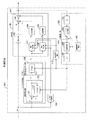
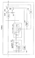
図2は、実施例1、実施例2及び実施例3で説明する干渉除去回路を適用したデジタル変調信号受信装置20の構成を示すブロック図である。図1は、実施例1における干渉除去回路100の構成を示すブロック図である。この実施例(以下の実施例も同様である)では発明の動作を理解し易いように、特に断らない限り受信信号として希望波にガードインターバルを超えた遅延時間を有する1波の遅延波が付加された信号を受信している場合を例として説明する。図1は、このような遅延波による干渉を除去するのに適した一例である。
FIG. 2 is a block diagram illustrating a configuration of a digital modulation
まずデジタル変調信号受信装置20を図2を用いて説明する。図2に示すデジタル変調信号受信装置20には、受信信号がA/D変換されて直交復調されたデジタル複素ベースバンド信号が入力される。入力されたデジタル複素ベースバンド信号は、干渉除去回路100に供給され、干渉除去回路100は、符号間干渉及びキャリア間干渉を除去した信号をFFT回路21に供給する。FFT回路21は図示しないシンボル同期信号発生部で生成されるシンボル同期信号に従って入力された信号からFFT期間を切り出して離散フーリエ変換を行い、得られた周波数軸上のベースバンド信号をSP等化回路22に供給する。SP等化回路22は、入力された信号に含まれるSP信号を基準として入力された信号を波形等化し、復調回路23に供給する。復調回路23は入力された信号を復調処理して、受信処理で得られた信号中の情報を再生し復調出力信号として出力する。
First, the digital modulation
次に、図1を用いてこの実施例における干渉除去回路100を説明する。干渉除去回路100は、入力された信号から伝送シンボルの切れ目を検出するシンボル位置検出器150と、入力された信号から反射波のレプリカ信号を生成するレプリカ生成部110と、反射波のレプリカ信号と入力信号を合成する合成部140と、合成部140の出力から伝送路応答を推定しレプリカ生成部110の特性を制御する係数算出部160と、係数算出部160の出力から遅延波の遅延時間を検出する遅延時間検出器170とから構成されている。
レプリカ生成部110は、波形等化部120と、反射波成分生成部130とから構成される。波形等化部120は、減算器122の出力が接続され係数算出部160により係数を可変されるFIRフィルタ121と、入力信号からFIRフィルタ121の出力を減ずる減算器122とから構成されている。反射波成分生成部130は、係数算出部160により係数を可変されるFIRフィルタ131から構成されている。FIRフィルタは、例えば、トランスバーサルフィルタで構成することができる。
Next, the
The replica generation unit 110 includes a
合成部140は、シンボル位置検出器150と、遅延時間検出器170の検出結果に基づいてレプリカ生成部110から供給された信号からその一部を切り出す信号切出器141、142と、信号切出器141、142の出力をそれぞれ所定時間遅延させる遅延回路144、145と、入力信号を所定時間遅延させる遅延回路143と、遅延回路143の出力に遅延回路144、145の出力をそれぞれ減算、加算して出力する減算器146と加算器147とから構成される。
係数算出部160は、合成部140の出力を離散フーリエ変換するFFT回路161と、その出力からパイロット信号を抽出するパイロット信号抽出器162と、抽出したパイロット信号に同期して伝送路歪がないときのパイロット信号に相当する基準信号を発生する基準信号発生器163と、抽出したパイロット信号から基準信号を減算する減算器164とその出力を基準信号で除算する複素除算器165と除算結果を逆離散フーリエ変換して出力するIFFT回路166から構成されている。
The
The
次に伝送路応答の推定の考え方を説明しながら係数算出部160及び遅延時間検出器170の動作について説明する。
図示しないデジタル放送送信装置で挿入する既知のパイロット信号の周波数特性を“R(ω)”とし、受信信号に含まれるパイロット信号の周波数特性を“S(ω)”とおく。伝送路における遅延波の周波数応答を“H(ω)”とすると、受信信号に含まれるパイロット信号は、
S(ω)=(1+H(ω))R(ω)…(1)
として、干渉除去回路100に入力される。干渉除去回路100は、入力された信号の周波数特性はそのままに、干渉成分のみを取り除くように動作するので、係数算出部160には“S(ω)”がそのまま供給され、パイロット信号抽出器162の出力として“S(ω)”を得ることができる。
Next, operations of the
A frequency characteristic of a known pilot signal inserted by a digital broadcast transmitting apparatus (not shown) is set to “R (ω)”, and a frequency characteristic of a pilot signal included in the received signal is set to “S (ω)”. If the frequency response of the delayed wave in the transmission path is “H (ω)”, the pilot signal included in the received signal is
S (ω) = (1 + H (ω)) R (ω) (1)
Is input to the
ここで基準信号発生器163から既知のパイロット信号の周波数特性“R(ω)”を供給すると複素除算器165の出力“D(ω)”は、
D(ω)=(S(ω)−R(ω))÷R(ω)=S(ω)÷R(ω)−1
…(2)
となる。ここで式(2)に式(1)を代入すると、
D(ω)=H(ω)…(3)
が導出される。すなわち、複素除算器165の出力“D(ω)”は遅延波の周波数応答“H(ω)”に等しくなり、それをIFFT回路166で逆離散変換した結果は、遅延波のインパルス応答を表すことになる。
また、デジタル放送送信装置の送信信号の周波数特性を“X(ω)”、受信信号の周波数特性を“Y(ω)”とおくと、
Y(ω)=(1+H(ω))X(ω)…(4)
で表すことができる。この信号が図1の波形等化部120に供給される。その出力信号を“Z(ω)”とする。
When the frequency characteristic “R (ω)” of the known pilot signal is supplied from the
D (ω) = (S (ω) −R (ω)) ÷ R (ω) = S (ω) ÷ R (ω) −1
... (2)
It becomes. When substituting equation (1) into equation (2),
D (ω) = H (ω) (3)
Is derived. That is, the output “D (ω)” of the
Further, if the frequency characteristic of the transmission signal of the digital broadcast transmission apparatus is “X (ω)” and the frequency characteristic of the reception signal is “Y (ω)”,
Y (ω) = (1 + H (ω)) X (ω) (4)
Can be expressed as This signal is supplied to the
FIRフィルタ121の周波数特性を“F(ω)”とおくと、波形等化部120の入出力特性は、
Z(ω)=Y(ω)−F(ω)Z(ω)…(5)
であるから、これを変形して、
Z(ω)=Y(ω)÷(1+F(ω))…(6)
で表すことができる。式(6)に式(4)を代入すると、
Z(ω)=((1+H(ω))÷(1+F(ω)))X(ω)…(7)
となり、送信信号“X(ω)”と波形等化部120の出力“Z(ω)”の関係が表現される。
ここで複素除算器165の出力“D(ω)”をIFFT回路166で逆離散変換した結果をFIRフィルタ121の係数として与える、すなわちF(ω)=D(ω)とすると、式(7)は、
Z(ω)=((1+H(ω))÷(1+D(ω)))X(ω)…(8)
となり、さらに式(8)に式(3)を代入すると、
Z(ω)=X(ω)…(8)
が得られる。
When the frequency characteristic of the
Z (ω) = Y (ω) −F (ω) Z (ω) (5)
So, transform this,
Z (ω) = Y (ω) ÷ (1 + F (ω)) (6)
Can be expressed as Substituting equation (4) into equation (6),
Z (ω) = ((1 + H (ω)) ÷ (1 + F (ω))) X (ω) (7)
Thus, the relationship between the transmission signal “X (ω)” and the output “Z (ω)” of the
Here, if the output “D (ω)” of the
Z (ω) = ((1 + H (ω)) ÷ (1 + D (ω))) X (ω) (8)
And further substituting equation (3) into equation (8),
Z (ω) = X (ω) (8)
Is obtained.
すなわち、上記動作により波形等化部120の出力に送信信号“X(ω)”が得られることになる。
なお、干渉除去回路が干渉除去を行っていない場合又は干渉除去が十分でない状態では、パイロット信号抽出器162の出力には誤差が含まれることになる。この場合、次式を用いてFIRフィルタ121の係数を更新する。
c(k+1)=c(k)+α×v(k)…(9)
ここで、v(k)は、k回目(kは正の整数)の係数算出部160の出力、c(k)は、FIRフィルタ121の係数、αは、1以下の定数である。
上記動作を繰り返すことで誤差が低減されるように動作し、干渉除去が行われる。なおαを小さくすれば伝送路の雑音の影響を受け難くなる。逆に、伝送路応答に時間的な変動がある場合にはαを大きくとるとよい。
That is, the transmission signal “X (ω)” is obtained at the output of the
Note that when the interference cancellation circuit does not perform interference cancellation or when interference cancellation is not sufficient, the output of the
c (k + 1) = c (k) + α × v (k) (9)
Here, v (k) is the output of the k-th (k is a positive integer)
By repeating the above operation, the operation is performed so that the error is reduced, and interference removal is performed. If α is made smaller, it will be less susceptible to the effects of transmission line noise. Conversely, if there is a temporal variation in the transmission line response, α should be increased.
また、係数算出部160の出力、すなわちIFFT回路166で逆離散変換した結果は、遅延時間検出器170に供給される。前述のように係数算出部160の出力は、遅延波のインパルス応答を表すので、例えば、その電力ピークから遅延波の遅延時間tdを知ることができる。そこで検出した遅延時間情報を信号切出器141と信号切出器142に供給する。
次に、図3を参照して図1の動作を説明する。図3は、図1に示した干渉除去回路が動作している時に流れている信号の一例を説明する図である。図3では連続する2つの伝送シンボルをクローズアップして図示している。
まず希望波に遅延時間td(td>Tg)の遅延波が付加された受信波(a)が受信され、干渉除去回路100に入力される。入力された受信波(a)は、シンボル位置検出器150と波形等化部120と合成部140に入力される。
シンボル位置検出器150は、入力された受信波(a)から希望波のシンボルの切れ目を検出してその位置情報を信号切出器141、142に供給する。シンボルの切れ目の検出方法としては、例えば、希望波のガードインターバルと有効シンボル後部の信号部分に相当する部分の相関が高いことを利用すればよい。
Further, the output of the
Next, the operation of FIG. 1 will be described with reference to FIG. FIG. 3 is a diagram for explaining an example of a signal that flows when the interference cancellation circuit shown in FIG. 1 is operating. In FIG. 3, two consecutive transmission symbols are shown in close-up.
First, a received wave (a) obtained by adding a delayed wave having a delay time td (td> Tg) to a desired wave is received and input to the
The
波形等化部120は、係数算出部160から供給されるフィルタ係数に基づいて受信波(a)に対して波形等化を行い等化信号(b)を反射波成分生成部130に供給する。係数算出部160から供給されるフィルタ係数は、遅延波の周波数応答“H(ω)”に等しいので、このフィルタ係数をFIRフィルタ131に与え、等化信号(b)をFIRフィルタ131に入力すると反射波のレプリカ信号を得ることができる。反射波成分生成部130は、このようにして得られる反射波のレプリカ信号(c)を合成部140に供給する。
The
合成部140では受信波(a)が遅延回路143に入力される。またレプリカ信号(c)が信号切出器141と信号切出器142に入力される。信号切出器141は、シンボルの位置情報と遅延時間情報に基づいて反射波のレプリカ信号(c)から注目する伝送シンボルの1つ前の伝送シンボルの後端にあたる部分を幅Teの期間(部分レプリカ信号1(d))を切り出して遅延回路144に供給する。ここで幅Teは、受信波(a)において符号間干渉を受けている期間の幅とする。図示したように伝送シンボルの後部をFFT期間とする場合には、Te=td−Tgで求められる。信号切出器142は、シンボルの位置情報と遅延時間情報に基づいて反射波のレプリカ信号(c)から注目する伝送シンボルの後端からTgだけ離れた部分を後端とした幅Teの期間(部分レプリカ信号2(e))を切り出して遅延回路145に供給する。このようにして得られた部分レプリカ信号1(d)は、図10で説明した1つ前の伝送シンボルに由来する信号成分(f)に相当するレプリカである。また部分レプリカ信号2(e)は、図10で説明した遅延波成分の連続性が欠落した部分に相当するレプリカである。よって受信波(a)とこれらの部分レプリカ信号を合成すればFFT期間における符号間干渉及びキャリア間干渉を取り除くことができる。
In the
そこで遅延回路143、144、145で入力された信号をそれぞれ所定時間だけ遅延させて信号間の遅延を合わせ、減算器146で受信波(a)の注目する伝送シンボルのFFT期間の先頭に あたる部分から部分レプリカ信号1(d)を減算し、さらに加算器147で注目する伝送シンボルのFFT期間の先頭にあたる部分に部分レプリカ信号2(e)を加算するように動作させる。すると合成部140の出力として受信波(a)からFFT期間内のキャリア間干渉成分及び符号間干渉成分が取り除かれた干渉除去出力(f)(図3ではFFT期間をクローズアップして図示している)が得られ、FFT回路161及び干渉除去回路の出力として図2に示したFFT回路21に供給される。
Therefore, the signals input by the
すなわち、合成部140は、受信波(a)において符号間干渉を受けている期間から符号間干渉及びキャリア間干渉を取り除くように反射波のレプリカ信号(c)の一部を合成し、合成しない期間は受信波(a)をそのまま出力するように動作する。この動作により、雑音や伝送路応答の時間的な変動により伝送路応答の推定に推定誤差が生じて反射波のレプリカ信号(c)に誤差が生じた場合であっても、その影響は、合成した期間に限定されるため、合成しなかった期間に新たな妨害を発生させることはなく、合成した期間内では誤差により干渉は完全には除去されないものの干渉成分が低減されることで、全体として受信性能が改善される。
また受信波(a)の伝送路応答を維持したまま干渉を低減するように動作するので、FFT後の周波数領域に現れる伝送路特性から復調結果の信頼性を算出することができ、その信頼性を算出して受信特性を改善するという従来技術をそのまま適用することができるという利点がある。
That is, the
Further, since the operation is performed to reduce the interference while maintaining the transmission path response of the received wave (a), the reliability of the demodulation result can be calculated from the transmission path characteristics appearing in the frequency domain after the FFT. There is an advantage that the conventional technique of improving the reception characteristic by calculating the above can be applied as it is.
なお、上記の例では遅延波が1波として説明したが複数の遅延波により符号間干渉を受けている場合も同様に実施できる。複数の遅延波がある場合は、最大の遅延時間を持つ遅延波に基づいて幅Teの期間を決めるとよい。
また合成する期間は上記で説明した幅Teに限られるものではない。
図3のレプリカ信号(c)と干渉除去出力(f)の関係に注目してみると、部分レプリカ信号1(d)と部分レプリカ信号2(e)は、上記で説明した幅Teに対し、前後に最大で幅Tgだけ余裕を持って切り出しても同様の効果が得られることが容易に推測される。例として前後に幅Tgだけ広く切り出す場合を図4で説明する。
In the above example, the delay wave has been described as one wave, but the same can be applied to the case where intersymbol interference is received by a plurality of delay waves. When there are a plurality of delay waves, the period of the width Te may be determined based on the delay wave having the maximum delay time.
Further, the synthesis period is not limited to the width Te described above.
When attention is paid to the relationship between the replica signal (c) and the interference removal output (f) in FIG. 3, the partial replica signal 1 (d) and the partial replica signal 2 (e) are equal to the width Te described above. It can be easily estimated that the same effect can be obtained even if the front and rear are cut out with a margin of the maximum width Tg. As an example, a case where the front and rear are cut out by a width Tg will be described with reference to FIG.
図4は、受信波(a)、等化信号(b)、レプリカ信号(c)が図3と同じであるので説明は省略する。図4の部分レプリカ信号1(d)は、反射波のレプリカ信号(c)から注目する伝送シンボルの1つ前の伝送シンボルの後端にあたる幅Teの期間を含み前後Tgだけ広げた期間を切り出した様子を示している。図4の部分レプリカ信号2(e)は、反射波のレプリカ信号(c)から注目する伝送シンボルの後端からTgだけ離れた部分を後端とした幅Teの期間を含み前後Tgだけ広げた期間を切り出した様子を示している。図4から分かるように、このようにして切り出した部分レプリカ信号1(d)と部分レプリカ信号2(e)の後部にあたる記号Aで表される部分は、同一の信号成分からなるので合成する際に互いに相殺される。よってこのような信号を受信波(a)に合成しても干渉除去出力(f)で示すように、FFT期間内からキャリア間干渉成分及び符号間干渉成分を取り除くことができる。このように合成する期間を伝送シンボルの端まで拡大すると伝送シンボル内のどの部分をFFT期間としてもよくなり、この発明による効果が得られるようになるという利点がある。更に図示は省略するが干渉除去出力(f)中の伝送シンボルの前端と後端が同じ特性になることから、前端の幅Tgの期間と後端のTgの期間を加算平均した信号をFFT期間に含む様にすればS/N改善効果が期待できる。 In FIG. 4, the received wave (a), the equalized signal (b), and the replica signal (c) are the same as those in FIG. The partial replica signal 1 (d) in FIG. 4 is extracted from the reflected wave replica signal (c) by including a period of width Te corresponding to the rear end of the transmission symbol immediately before the transmission symbol of interest and extending it by the front and rear Tg. It shows the state. The partial replica signal 2 (e) in FIG. 4 is expanded by the front and rear Tg including the period of the width Te with the portion separated from the rear end of the transmission symbol of interest by Tg from the replica signal (c) of the reflected wave as the rear end. It shows how the period is cut out. As can be seen from FIG. 4, the portion represented by the symbol A, which is the rear portion of the partial replica signal 1 (d) and the partial replica signal 2 (e) cut out in this way, is composed of the same signal component, so Offset each other. Therefore, even when such a signal is combined with the received wave (a), the inter-carrier interference component and the inter-symbol interference component can be removed from the FFT period as indicated by the interference removal output (f). When the combining period is extended to the end of the transmission symbol in this way, any part in the transmission symbol may be used as the FFT period, and the advantage of the present invention can be obtained. Further, although not shown, since the front end and the rear end of the transmission symbol in the interference cancellation output (f) have the same characteristics, a signal obtained by averaging the period of the width Tg of the front end and the period of Tg of the rear end is an FFT period. If included, an S / N improvement effect can be expected.
また合成する期間を後ろに広げてもよいので設計の自由度が広がるという利点がある。例えば、対応する遅延波の遅延時間が2×Tg以下でよいのであれば、FFT期間の先頭から幅Tgの期間に対応する部分レプリカ信号1(d)と部分レプリカ信号1(e)を生成して合成すればよいので、切り出す幅を一定として設計することができる。この場合遅延時間tdを検出する必要がなくなるので遅延時間検出回路170を不要にすることができるという利点がある。
In addition, since the synthesis period may be extended backward, there is an advantage that the degree of freedom of design is expanded. For example, if the delay time of the corresponding delayed wave may be 2 × Tg or less, the partial replica signal 1 (d) and the partial replica signal 1 (e) corresponding to the period of the width Tg from the beginning of the FFT period are generated. Therefore, the width to be cut out can be designed to be constant. In this case, there is an advantage that the delay
本発明は、この実施例のものに限定されるものではない。本発明の要旨を鑑みれば実施例を元にした様々な変形が容易に考えられるし、その場合でも同様の効果を得られることは勿論である。例えば、レプリカ生成部110は、必ずしも波形等化部120と反射波成分生成部130とに分けて構成する必要は無いので、前記実施例においてFIRフィルタ121とFIRフィルタ131は分かり易いように別々の構成要素として説明したが、2つのFIRフィルタが同じ信号が入力され同一の特性でよいことを利用して1つのFIRフィルタで構成してもよい。また合成部140は、同様の動作を実現できるならば、例えば、あらかじめレプリカ信号を切り出しておいてから合成するのではなく、受信波とレプリカ信号を全期間に渡って合成しておいた結果と受信波とを適宜選択して出力するような回路で構成することができるのは容易に推測される。またこの実施例において説明した伝送路の推定方法は1つの例であり、他の伝送路の推定手法を用いてもよい。更には波形等化部120は、フィードバック型の波形等化器を用いて説明したが、フィードフォワード型の波形等化器を用いても発明を実施できることは勿論である。フィードフォワード型の波形等化器を用いることで、希望波よりも到達時間の早い反射波による符号間干渉を除去したい場合にも本発明を適応することが可能になる。
The present invention is not limited to this embodiment. In view of the gist of the present invention, various modifications based on the embodiments can be easily considered, and even in that case, the same effect can be obtained. For example, since the replica generation unit 110 does not necessarily have to be configured separately from the
また本実施例において説明した伝送路の推定方法はごく一例であり、他の伝送路の推定手法を用いてもよいのは勿論である。式(2)のように直接的に適応フィルタの特性を算出するアルゴリズムを最小二乗誤差法などの逐次修正型のアルゴリズムに対して直接解法型アルゴリズムと呼ぶ。ここでは説明しないが波形等化部120で誤差を定義して最小二乗誤差法などの逐次修正型のアルゴリズムを適用してもよい。本発明を実施するにあたりいずれのアルゴリズムを採用するかは設計事項であるが、直接解法型アルゴリズムは一般に逐次型のアルゴリズムよりも伝送路応答の変動に高速追従させ易いという利点がある。
さらにはレプリカ信号の作成方法や合成方法にも様々なバリエーションを取りうる。そしてそのような実施方法でも本発明による効果を得ることができるのは勿論である。
Further, the transmission path estimation method described in the present embodiment is only an example, and it is needless to say that other transmission path estimation methods may be used. An algorithm that directly calculates the characteristics of the adaptive filter as expressed by equation (2) is called a direct solution type algorithm for a sequential correction type algorithm such as the least square error method. Although not described here, an error may be defined by the
Furthermore, various variations can be taken in the method of creating and synthesizing the replica signal. Of course, the effect of the present invention can be obtained even by such an implementation method.
次に、図5及び図6を参照して実施例2を説明する。
具体的にレプリカ信号の作成方法や合成方法を変えた他の実施例を説明する。この実施例では、先に受信波を有効シンボル期間だけ遅延させた信号と受信波との差をとってから、その差信号を元にレプリカ信号を作成することを特徴としている。また受信波とレプリカ信号を全期間に渡って合成した結果と受信波とを適宜選択して出力する場合としても例示している。
図5は、実施例2における干渉除去回路の構成を示すブロック図である。この干渉除去回路は、図2に示したデジタル変調信号受信装置20に適用される。
干渉除去回路は、入力された信号から伝送シンボルの切れ目を検出するシンボル位置検出器150と、入力された信号とそれを有効シンボル期間の時間だけ遅延させた信号との差(シンボル間差信号)を出力するシンボル間差信号生成回路570と、シンボル間差信号から反射波のレプリカ信号を生成するレプリカ生成部510と、反射波のレプリカ信号と入力信号を合成する合成部540と、合成部540の出力から伝送路応答を推定しレプリカ生成部510の特性を制御する係数算出部160と、係数算出部160の出力から遅延波の遅延時間を検出する遅延時間検出器170とから構成されている。
Next, Example 2 will be described with reference to FIGS.
Specifically, another embodiment in which a replica signal creation method and synthesis method are changed will be described. This embodiment is characterized in that a replica signal is created based on a difference between a signal obtained by previously delaying a received wave by an effective symbol period and a received wave. Further, the case where the result of combining the received wave and the replica signal over the entire period and the received wave are appropriately selected and output is also illustrated.
FIG. 5 is a block diagram illustrating the configuration of the interference cancellation circuit according to the second embodiment. This interference canceling circuit is applied to the digital modulation
The interference cancellation circuit detects a difference between the input signal and a signal obtained by delaying the input signal by a time of an effective symbol period (inter-symbol difference signal). The symbol difference
シンボル間差信号生成回路570は、入力信号を有効シンボル期間だけ遅延させる遅延回路571と、入力信号から遅延信号を減ずる減算器572とから構成される。
レプリカ生成部510は、減算器512の出力が接続され係数算出部160により係数を可変されるFIRフィルタ511と、入力信号からFIRフィルタ511の出力を減ずる減算器512とから構成される。
合成部540は、入力信号を所定時間遅延させる遅延回路541と、遅延回路541の出力にレプリカ生成部510から供給された信号を加算する加算器542と、シンボル位置検出器150と遅延時間検出器170の検出結果に基づいて遅延回路541の出力と加算器542の出力を選択して出力する信号選択回路543から構成される。
シンボル位置検出器150と係数算出部160及び遅延時間検出器170は実施例1で図1に示した同じ符号を付した構成要素と同じ構成、同じ動作でよいので個々の説明は省略する。
The inter-symbol difference
The replica generation unit 510 includes an
The combining
The
次に本実施例における図5の動作について図6を参照して説明する。図6は、図5に示した干渉除去回路が動作している時に流れている信号の一例を説明する図である。図6では連続する2つの伝送シンボルをクローズアップして図示している。
まず希望波に遅延時間td(td>Tg)の遅延波が付加された受信波(a)が受信され、干渉除去回路に入力される。入力された受信波(a)は、シンボル位置検出器150とシンボル間差信号生成回路570と合成部540に入力される。
シンボル位置検出器150は、入力された受信波(a)から希望波のシンボルの切れ目を検出してその位置情報を信号選択回路543に供給する。
Next, the operation of FIG. 5 in the present embodiment will be described with reference to FIG. FIG. 6 is a diagram for explaining an example of signals flowing when the interference cancellation circuit shown in FIG. 5 is operating. In FIG. 6, two consecutive transmission symbols are shown in close-up.
First, a received wave (a) obtained by adding a delayed wave having a delay time td (td> Tg) to a desired wave is received and input to an interference cancellation circuit. The input received wave (a) is input to the
The
シンボル間差信号生成回路570は、受信波(a)を遅延回路571で有効シンボル期間(伝送シンボルからガードインターバルを除いた期間)に相当する時間だけ遅延させ(有効シンボル遅延信号(b))、減算器572で入力信号から有効シンボル遅延信号(b)を減じて、有効シンボル間差信号(c)をレプリカ生成部510に供給する。図6からわかるように受信波(a)に含まれる希望波のガードインターバル期間と、有効シンボル遅延信号(b)のガードインターバルと同じ信号成分を持つ有効シンボルの後部が時間的に一致することになるので、減算することで取り除かれる。遅延波についても同様である。図示する際には有効シンボル間差信号(c)のごとく打ち消しあった信号成分は、隙間を開けて表現することにする。
The inter-symbol difference
レプリカ生成部510は、実施例1で説明したレプリカ生成部110をFIRフィルタ1つで表現した例であり、レプリカ係数算出部160から供給されるフィルタ係数をFIRフィルタ511に与えることで、有効シンボル間差信号(c)から差信号のレプリカ信号(d)を生成して合成部540に供給することができる。差信号のレプリカ信号(d)は、FIRフィルタ511の出力として取り出される。ここで生成する差信号のレプリカ信号(d)は、有効シンボル間差信号(c) に含まれる遅延波成分に相当する信号である。
合成部540では受信波(a)が遅延回路541に入力され、遅延回路541は受信波(a)を有効シンボル期間に相当する時間だけ遅延させる(遅延信号(e))。加算器542は、遅延信号(e)と差信号のレプリカ信号(d)とを加算して信号選択回路543に供給する。信号選択回路543は、シンボルの位置情報と遅延時間情報に基づいて、FFT期間の前端から幅Teの期間は加算器542から信号を出力し、それ以外の期間は遅延回路541からの信号を選択して出力するように動作する。この選択の様子は、選択信号(f)のように表現できる。ここで幅Teは、受信波(a)において符号間干渉を受けている期間の幅とする。図示したように伝送シンボルの後部をFFT期間とした場合には、Te=td−Tgで求められる。
The replica generation unit 510 is an example in which the replica generation unit 110 described in the first embodiment is expressed by one FIR filter. By supplying the filter coefficient supplied from the replica
In the combining
すなわち、合成部540は、受信波(a)において符号間干渉を受けている期間は符号間干渉及びキャリア間干渉を取り除くように差信号のレプリカ信号(d)を合成した結果を出力し、それ以外の期間は、受信波(a)をそのまま出力するように動作する。この動作により、雑音や伝送路応答の時間的な変動により伝送路応答の推定に推定誤差が生じて差信号のレプリカ信号(d)に誤差が生じた場合であっても、その影響は合成した期間に限定されるため、合成しなかった期間に新たな妨害を発生させることはなく、合成した期間内では誤差により干渉は完全には除去されないものの干渉成分が低減されることにより受信性能が改善される。また合成した結果を出力する期間は、上記で説明した幅Teに限られるものではなく実施例1の説明と同様に前後に最大で幅Tgだけ余裕を持って合成結果を出力しても同様の効果が得られることは勿論である。
また本実施例においても様々な変形が容易に考えられるし、その場合でも同様の効果を得られることは勿論である。例えば、遅延回路571と遅延回路541は分かり易いように別々の構成要素として説明したが、2つの遅延回路が同じ信号が入力され同じ遅延時間でよいことに着目して1つの遅延回路で構成してもよい。
That is, the combining
Also, in this embodiment, various modifications can be easily considered, and even in this case, the same effect can be obtained. For example, the
次に、図7、図8を用いて実施例3を説明する。
レプリカ信号の作成方法や合成方法を変えた他の実施例を説明する。この実施例では、信号切出器を反射波成分生成部の前に設けたことに特徴である。このように構成することで遅延時間検出回路を不要とすることができる。
図7は本実施例における干渉除去回路の構成を示すブロック図である。本干渉除去回路は図2に示したデジタル変調信号受信装置20に適用される。
干渉除去回路は、入力された信号から伝送シンボルの切れ目を検出するシンボル位置検出器150と、入力された信号とそれを有効シンボル期間の時間だけ遅延させた信号との差(シンボル間差信号)を出力するシンボル間差信号生成回路570と、シンボル間差信号から反射波の部分レプリカ信号を生成するレプリカ生成部710と、反射波の部分レプリカ信号と入力信号を合成する合成部740と、合成部740の出力から伝送路応答を推定しレプリカ生成部510の特性を制御する係数算出部160とから構成されている。
レプリカ生成部710は、入力されたシンボル間差信号を波形等化する波形等化部120と、波形等化部120の出力信号の一部を切り出す信号切出器711と、信号切出器711の出力から反射波の部分レプリカ信号を生成して出力する反射波成分生成部130とから構成される。
Next, Example 3 will be described with reference to FIGS.
Another embodiment in which the replica signal creation method and synthesis method are changed will be described. This embodiment is characterized in that a signal extractor is provided in front of the reflected wave component generator. With this configuration, the delay time detection circuit can be eliminated.
FIG. 7 is a block diagram showing the configuration of the interference cancellation circuit in this embodiment. This interference canceling circuit is applied to the digital modulation
The interference cancellation circuit detects a difference between the input signal and a signal obtained by delaying the input signal by a time of an effective symbol period (inter-symbol difference signal). A symbol difference
The
合成部740は、入力信号を所定時間遅延させる遅延回路741と、シンボル位置検出器150の検出結果に基づいて反射波の部分レプリカ信号からその一部を切り出す信号切出器742と、遅延回路741の出力と信号切出器742の出力を加算して出力する加算器743とから構成される。
シンボル位置検出器150、シンボル間差信号生成回路570、波形等化部120、反射波成分生成部130及び係数算出部160は、実施例1における図1又は実施例2における図5に示した同じ符号を付した構成要素と同じ構成、同様の動作でよいので詳細な説明は省略する。
次に本実施例における図7の動作について図8を用いて説明する。図8は、図7に示した干渉除去回路が動作している時に流れている信号の一例を説明する図である。図8では連続する2つの伝送シンボルをクローズアップして図示している。
まず希望波に遅延時間td(td>Tg)の遅延波が付加された受信波(a)が受信され、干渉除去回路に入力される。入力された受信波(a)は、シンボル位置検出器150とシンボル間差信号生成回路570と合成部740に入力される。
The
The
Next, the operation of FIG. 7 in the present embodiment will be described with reference to FIG. FIG. 8 is a diagram illustrating an example of a signal that flows when the interference cancellation circuit illustrated in FIG. 7 is operating. In FIG. 8, two consecutive transmission symbols are shown in close-up.
First, a received wave (a) obtained by adding a delayed wave having a delay time td (td> Tg) to a desired wave is received and input to an interference cancellation circuit. The input received wave (a) is input to the
シンボル位置検出器150は、入力された受信波(a)から希望波のシンボルの切れ目を検出してその位置情報を信号切出器711と信号切出器742に供給する。
シンボル間差信号生成回路570は、受信波(a)から有効シンボル間差信号(b)を生成し、レプリカ生成部710に供給する。
レプリカ生成部710に供給された有効シンボル間差信号(b)は、波形等化部120に入力され、波形等化部120は、係数算出部160から供給されるフィルタ係数に基づいて有効シンボル間差信号(b)に対して波形等化を行い、等化信号(c)を信号切出器711に供給する。
信号切出器711は、シンボルの位置情報に基づいて等化信号(c)から幅Taの期間を切り出した信号(部分等化信号(d))を反射波成分生成部130に供給する。幅Taの期間は、例えば、注目する伝送シンボルの後端からTgだけ離れた部分を後端とし、Ts/2の幅とするのが適当である。この場合、遅延時間がTs/2以下の反射波に対して効果を得ることができる。
The
The inter-symbol difference
The effective inter-symbol difference signal (b) supplied to the
The
反射波成分生成部130は、係数算出部160から供給されるフィルタ係数をFIRフィルタ131に与えることで、部分等化信号(d)から部分レプリカ信号1(e)を生成して合成部740に供給する。
合成部740では受信波(a)が遅延回路741に入力され、遅延回路741は受信波(a)を有効シンボル期間に相当する時間だけ遅延させた信号(遅延信号(g))を加算器743に供給する。また部分レプリカ信号1(e)が信号切出器742に入力され、信号切出器742は、シンボルの位置情報に基づいて反射波の部分レプリカ信号1(e)から幅Tbの期間を切り出した信号(部分レプリカ信号2(e))を加算器743に供給する。幅Tbの期間は、例えば、遅延信号(g)の対応する伝送シンボルの先頭から幅Ts/2の期間に相当する期間とするのが適当である。
加算器743は、入力された遅延信号(g)と部分レプリカ信号2(e)を加算する。この結果、合成部740の出力として受信波(a)からキャリア間干渉成分及び符号間干渉成分が取り除かれた干渉除去出力(h)が得られ、干渉除去回路の出力として図2に示したFFT回路21に供給される。
The reflected wave component generation unit 130 gives the filter coefficient supplied from the
In the combining
The
すなわち、合成部740は、受信波(a)の符号間干渉を受けている期間を含む期間では部分レプリカ信号1(e)を合成して符号間干渉及びキャリア間干渉を取り除いた結果を出力し、それ以外の期間では受信波(a)をそのまま出力するように動作する。この動作により、雑音や伝送路応答の時間的な変動により伝送路応答の推定に推定誤差が生じて差信号の部分レプリカ信号1(e)に誤差が生じた場合であっても、その影響は合成した期間に限定されるため、合成しなかった期間に新たな妨害を発生させることはなく、合成した期間内では誤差により干渉は完全には除去されないものの干渉成分が低減されることで受信性能が改善される。
また、この実施例においても様々な変形が容易に考えられるし、その場合でも同様の効果を得られることは勿論である。例えば、遅延回路571と遅延回路741は、分かり易いように別々の構成要素として説明したが、2つの遅延回路が同じ信号が入力され同じ遅延時間でよいことに着目して1つの遅延回路で構成してもよい。
That is, the combining
Also, in this embodiment, various modifications can be easily considered, and even in this case, the same effect can be obtained. For example, the
また、上記の実施例1,2,3において、説明し易いように遅延時間td(td>Tg)の遅延波が付加された受信波を受信する場合について説明したが、本発明はこのようなガードインターバル長を超える遅延波を受信する場合に限定されるものではない。例えば、伝送シンボルの中央をFFT期間とした場合は、遅延時間td(td>Tg/2)の遅延波によりFFT期間が符号間干渉を受けるし、本発明を適応して効果が得られることは容易に理解できるであろう。また実施例3は遅延時間td(Ts/2>td>0)の反射波に対して効果が得られるように動作可能である。更に実施例1でも説明したように、フィードフォワード型の波形等化器を用いれば、希望波よりも到達時間の早い反射波による符号間干渉を除去したい場合にも本発明を適応して効果が得られるのである。更にはガードインターバル長にこだわる必要はないのでガードインターバルを設けないOFDM信号を受信する場合にも本発明を適用でき、効果が得られることは容易に理解できるであろう。
また、本発明は、OFDMを受信する受信装置に限定されるものではなく、他の種類のマルチキャリア変調信号を受信する受信装置にも適用することができる。前記実施例を鑑みれば、マルチキャリア変調信号を受信して受信した信号をフーリエ変換により時間領域から周波数領域に変換して復調するデジタル変調信号受信装置に本発明を適用することができることは容易に理解できるであろう。すなわちフーリエ変換の前にフーリエ変換する期間のうち符号間干渉を受けている期間を含む一部の期間だけに受信信号の伝送路応答に基づいて受信信号から生成した干渉除去成分を合成し、それ以外の期間には何もしないようにすればよい。このような処理は、専用のハードウェアを用いなくともソフトウェア処理でも実施できることは勿論であり、同様に本発明の効果を得ることができる。
In the first, second, and third embodiments, the case where a reception wave to which a delay wave having a delay time td (td> Tg) is added has been described for ease of explanation. The present invention is not limited to the case of receiving a delayed wave exceeding the guard interval length. For example, when the center of a transmission symbol is an FFT period, the FFT period is subject to intersymbol interference due to a delay wave having a delay time td (td> Tg / 2), and the effect can be obtained by applying the present invention. It will be easy to understand. Further, the third embodiment can operate so as to obtain an effect on the reflected wave having the delay time td (Ts / 2>td> 0). Further, as described in the first embodiment, if a feedforward type waveform equalizer is used, the present invention can be applied and effective even when it is desired to remove intersymbol interference caused by a reflected wave having an arrival time earlier than the desired wave. It is obtained. Furthermore, since it is not necessary to pay attention to the guard interval length, it can be easily understood that the present invention can be applied to the case where an OFDM signal without a guard interval is received and the effect is obtained.
Further, the present invention is not limited to a receiving apparatus that receives OFDM, but can also be applied to receiving apparatuses that receive other types of multicarrier modulation signals. In view of the above-described embodiment, it is easy to apply the present invention to a digital modulation signal receiving apparatus that receives and receives a multicarrier modulation signal and converts the received signal from the time domain to the frequency domain by Fourier transform and demodulates it. You can understand. That is, the interference cancellation component generated from the received signal is synthesized based on the transmission path response of the received signal only during a part of the period including the period in which intersymbol interference is received among the period of Fourier transform before the Fourier transform. Do nothing during other periods. Such processing can be performed by software processing without using dedicated hardware, and the effects of the present invention can be obtained in the same manner.
本発明は、以下のような態様が例示される。
(1) マルチキャリア変調信号を受信して、フーリエ変換により受信信号を時間領域から周波数領域に変換して復調するデジタル変調信号受信装置において、フーリエ変換より前段に符号間干渉又はキャリア間干渉を低減する干渉除去手段を有することを特徴としたデジタル変調信号受信装置。(2) 前記干渉除去手段は前記受信信号から推定される伝送路応答に基づいて前記受信信号に時間領域で信号処理を施して干渉を低減することを特徴とした(1)のデジタル変調信号受信装置。(3) 前記干渉除去手段は前記受信信号の伝送路応答を維持したまま干渉を低減するように動作することを特徴とした(1)又は(2)のデジタル変調信号受信装置。
The following aspects of the present invention are exemplified.
(1) In a digital modulation signal receiving apparatus that receives a multicarrier modulation signal and demodulates the received signal from the time domain to the frequency domain by Fourier transform, the intersymbol interference or intercarrier interference is reduced before the Fourier transform. An apparatus for receiving a digital modulation signal, characterized by comprising interference canceling means. (2) The digitally modulated signal reception according to (1), wherein the interference canceling means performs signal processing in the time domain on the received signal based on a transmission path response estimated from the received signal to reduce interference. apparatus. (3) The digitally modulated signal receiver according to (1) or (2), wherein the interference canceling unit operates to reduce interference while maintaining a transmission path response of the received signal.
(4) マルチキャリア変調信号を受信して、フーリエ変換により受信信号を時間領域から周波数領域に変換して復調するデジタル変調信号受信装置において、フーリエ変換の前段に符号間干渉又はキャリア間干渉を低減する干渉除去手段をそなえ、前記干渉除去手段はフーリエ変換する期間ごとに符号間干渉又はキャリア間干渉を受けている期間を含む適当な期間だけに受信信号の伝送路応答に基づいて受信信号から生成した干渉除去成分を合成し、それ以外の期間は受信信号をそのまま出力するようにしたことを特徴とするデジタル変調信号受信装置。(5) 前記干渉除去手段は、受信信号から干渉除去成分を生成するレプリカ生成手段と、干渉除去成分と受信信号を合成する合成手段と、受信信号から伝送路応答を推定しレプリカ生成手段の特性を制御する制御手段を備えることを特徴とする(4)のデジタル変調信号受信装置。(6) 前記制御手段は、前記干渉除去手段の出力信号から伝送路応答を推定することを特徴とする(5)のデジタル変調信号受信装置。(7) 前記フーリエ変換をFFTで行うことを特徴とする(1)〜(6)のデジタル変調信号受信装置。 (4) In a digital modulation signal receiving apparatus that receives a multi-carrier modulation signal, demodulates the received signal from the time domain to the frequency domain by Fourier transform, and reduces intersymbol interference or inter-carrier interference before the Fourier transform. The interference canceling means is generated from the received signal based on the transmission line response of the received signal only during an appropriate period including the period receiving intersymbol interference or intercarrier interference every Fourier transform period. A digital modulation signal receiving apparatus characterized in that the interference cancellation components are combined and the received signal is output as it is during other periods. (5) The interference canceling means includes a replica generating means for generating an interference canceling component from the received signal, a combining means for combining the interference canceling component and the received signal, and a characteristic of the replica generating means by estimating a transmission line response from the received signal. (4) The digital modulation signal receiving apparatus according to (4), further comprising control means for controlling (6) The digital modulation signal receiving apparatus according to (5), wherein the control means estimates a transmission path response from the output signal of the interference removal means. (7) The digitally modulated signal receiver according to (1) to (6), wherein the Fourier transform is performed by FFT.
(8) マルチキャリア変調信号を受信して、フーリエ変換により受信信号を時間領域から周波数領域に変換して復調するデジタル変調信号受信方法において、フーリエ変換をする前に符号間干渉又はキャリア間干渉を低減することを特徴としたデジタル変調信号受信方法。(9) 前記受信信号から推定される伝送路応答に基づいて前記受信信号に時間領域処理を施して干渉を低減することを特徴とした請求項第8項記載のデジタル変調信号受信方法。(10) 前記受信信号の伝送路応答を維持したまま干渉を低減することを特徴とした(8)又は(9)のデジタル変調信号受信方法。
(8) In a digital modulation signal receiving method for receiving a multicarrier modulation signal and demodulating the received signal from the time domain to the frequency domain by Fourier transform, intersymbol interference or intercarrier interference is performed before Fourier transform. A method for receiving a digital modulation signal, characterized in that it is reduced. (9) The digital modulation signal receiving method according to
(11) マルチキャリア変調信号を受信して、フーリエ変換により受信信号を時間領域から周波数領域に変換して復調するデジタル変調信号受信方法において、受信信号の伝送路応答に基づいて受信信号から生成した干渉除去成分を、受信信号の符号間干渉又はキャリア間干渉を受けている期間を含む適当な期間だけに合成し、それ以外の期間は合成しないことを特徴とするデジタル変調信号受信方法。(12) 前記デジタル変調信号受信方法は、干渉除去後の信号から伝送路応答を推定することを特徴とする(11)のデジタル変調信号受信方法。(13) 前記フーリエ変換をFFTで行うことを特徴とする(1)〜(12)のデジタル変調信号受信装置又はデジタル変調信号受信方法。(14) 前記マルチキャリア変調信号がOFDMであることを特徴とする(1)〜(13)のデジタル変調信号受信装置又はデジタル変調信号受信方法。(15) 直接解法アルゴリズムを用いることを特徴とする(1)〜(14)のデジタル変調信号受信装置又はデジタル変調信号受信方法。 (11) In a digital modulation signal receiving method for receiving a multicarrier modulation signal and demodulating the received signal by transforming it from the time domain to the frequency domain by Fourier transform, it is generated from the received signal based on the transmission path response of the received signal A method for receiving a digital modulated signal, wherein the interference cancellation component is synthesized only during an appropriate period including a period during which inter-symbol interference or inter-carrier interference is received in the received signal, and is not synthesized during other periods. (12) The digital modulation signal reception method according to (11), wherein the digital modulation signal reception method estimates a transmission path response from the signal after interference cancellation. (13) The digital modulation signal receiving apparatus or digital modulation signal receiving method according to (1) to (12), wherein the Fourier transform is performed by FFT. (14) The digital modulation signal receiving apparatus or digital modulation signal receiving method according to (1) to (13), wherein the multicarrier modulation signal is OFDM. (15) The digital modulation signal receiving apparatus or digital modulation signal receiving method according to any one of (1) to (14), wherein a direct solution algorithm is used.
上記(1)、(2)又は(8)、(9)によれば、フーリエ変換より前に時間領域で干渉除去を行うことで符号間干渉やキャリア間干渉を除去することができ、受信性能の改善がはかられる。その結果、追従性の向上とキャンセル可能な遅延時間の拡大とを両立するデジタル変調信号受信装置が得られる。(3)又は(10)によれば、受信信号の伝送路応答が維持されるので、フーリエ変換後の周波数領域に現れる伝送路特性から復調結果の信頼性を算出することができ、その信頼性を算出して受信特性を改善するという従来技術をそのまま適用することができるという利点がある。 According to the above (1), (2), (8), and (9), it is possible to remove intersymbol interference and intercarrier interference by performing interference removal in the time domain before Fourier transform, and reception performance. Can be improved. As a result, it is possible to obtain a digital modulation signal receiving apparatus that achieves both improvement in followability and expansion of cancelable delay time. According to (3) or (10), since the transmission path response of the received signal is maintained, the reliability of the demodulation result can be calculated from the transmission path characteristics appearing in the frequency domain after Fourier transform. There is an advantage that the conventional technique of improving the reception characteristic by calculating the above can be applied as it is.
(4)又は(11)によれば、受信信号の伝送路応答が維持されるので、フーリエ変換後の周波数領域に現れる伝送路特性から復調結果の信頼性を算出することができ、その信頼性を算出して受信特性を改善するという従来技術をそのまま適用することができるという利点がある。(15)によれば、直接解法アルゴリズムを用いることで逐次型アルゴリズムよりも伝送路応答の変動に高速追従させやすいという利点がある。 According to (4) or (11), since the transmission path response of the received signal is maintained, the reliability of the demodulation result can be calculated from the transmission path characteristics appearing in the frequency domain after Fourier transform. There is an advantage that the conventional technique of improving the reception characteristic by calculating the above can be applied as it is. According to (15), there is an advantage that it is easy to follow the fluctuation of the transmission line response at a higher speed than the sequential algorithm by using the direct solution algorithm.
20…デジタル変調信号受信装置、21…FFT回路、22…SP等化回路、23…復調回路、100…干渉除去回路、110…レプリカ生成部、120…波形等化部、121…FIRフィルタ、122…減算器、130…反射波成分生成部、131…FIRフィルタ、140…合成部、141…信号切出器、142…信号切出器、144…遅延回路、145…遅延回路、146…減算器、147…加算器、150…シンボル位置検出器、160…係数算出部、161…FFT回路、162…パイロット信号抽出器、163…基準信号発生器、164…減算器、165…複素除算器、166…IFFT回路、170…遅延時間検出器。
DESCRIPTION OF
Claims (2)
Priority Applications (4)
| Application Number | Priority Date | Filing Date | Title |
|---|---|---|---|
| JP2005183007A JP5072199B2 (en) | 2005-06-23 | 2005-06-23 | Digital modulation signal receiving apparatus and receiving method thereof |
| US11/472,351 US8345802B2 (en) | 2005-06-23 | 2006-06-22 | Receiver for digital modulated signal and receiving method for the same |
| EP06013015.0A EP1737177A3 (en) | 2005-06-23 | 2006-06-23 | Receiver for digital modulated signal and receiving method for the same |
| CN2006100932406A CN1885840B (en) | 2005-06-23 | 2006-06-23 | Receiver for digital modulated signal and receiving method for the same |
Applications Claiming Priority (1)
| Application Number | Priority Date | Filing Date | Title |
|---|---|---|---|
| JP2005183007A JP5072199B2 (en) | 2005-06-23 | 2005-06-23 | Digital modulation signal receiving apparatus and receiving method thereof |
Publications (2)
| Publication Number | Publication Date |
|---|---|
| JP2007006067A JP2007006067A (en) | 2007-01-11 |
| JP5072199B2 true JP5072199B2 (en) | 2012-11-14 |
Family
ID=37075208
Family Applications (1)
| Application Number | Title | Priority Date | Filing Date |
|---|---|---|---|
| JP2005183007A Active JP5072199B2 (en) | 2005-06-23 | 2005-06-23 | Digital modulation signal receiving apparatus and receiving method thereof |
Country Status (4)
| Country | Link |
|---|---|
| US (1) | US8345802B2 (en) |
| EP (1) | EP1737177A3 (en) |
| JP (1) | JP5072199B2 (en) |
| CN (1) | CN1885840B (en) |
Families Citing this family (20)
| Publication number | Priority date | Publication date | Assignee | Title |
|---|---|---|---|---|
| US7844018B2 (en) * | 2007-01-02 | 2010-11-30 | Qualcomm Incorporated | Methods and apparatuses for reducing inter-carrier interference in an OFDM system |
| JP5242924B2 (en) * | 2007-02-26 | 2013-07-24 | Necディスプレイソリューションズ株式会社 | Video display system, video signal transmitter and video display device |
| JP4963723B2 (en) * | 2007-06-19 | 2012-06-27 | シャープ株式会社 | Receiver, receiving method and integrated circuit |
| US20100183094A1 (en) * | 2007-06-26 | 2010-07-22 | Kazuyuki Shimezawa | Reception device and reception method |
| JP5030312B2 (en) * | 2007-09-05 | 2012-09-19 | シャープ株式会社 | Receiver, receiving method and integrated circuit |
| US8571136B1 (en) * | 2007-11-21 | 2013-10-29 | University Of South Florida | Adaptive symbol transition method for OFDM-based cognitive radio systems |
| US8139664B2 (en) | 2007-11-28 | 2012-03-20 | Sony Corporation | Reception apparatus, reception method and program |
| JP2009186241A (en) * | 2008-02-04 | 2009-08-20 | Sumitomo Electric Ind Ltd | Receiving device range-finding system, positioning system, computer program, and reception time point determining method |
| CN101971536B (en) | 2008-02-27 | 2015-10-21 | 松下电器产业株式会社 | Receiving system, integrated circuit and method of reseptance |
| KR101138602B1 (en) * | 2008-04-17 | 2012-04-26 | 주식회사 코아로직 | Orthogonal frequency division multiplexingOFDM receiving apparatus and method of minimizing inter symbol interferenceISI using the same the apparatus |
| JP4569695B2 (en) * | 2008-09-19 | 2010-10-27 | ソニー株式会社 | Equalizer, equalization method, program, receiver |
| JP5644475B2 (en) | 2010-02-18 | 2014-12-24 | 富士通株式会社 | Receiver |
| US8655282B2 (en) * | 2010-10-29 | 2014-02-18 | Qualcomm Incorporated | Multiple signal transformation in wireless receivers |
| JP2012204941A (en) * | 2011-03-24 | 2012-10-22 | Toshiba Corp | Receiving device and receiving method |
| US20120295565A1 (en) * | 2011-05-16 | 2012-11-22 | Raytheon Company | System and method for analog interference suppression in pulsed signal processing |
| US8614940B1 (en) | 2012-11-14 | 2013-12-24 | The Aerospace Corporation | Systems and methods for reducing narrow bandwidth interference contained in broad bandwidth signals |
| WO2017221427A1 (en) * | 2016-06-24 | 2017-12-28 | 株式会社ソシオネクスト | Equalization circuit, reception circuit and integrated circuit device |
| US9628122B1 (en) | 2016-07-25 | 2017-04-18 | The Aerospace Corporation | Circuits and methods for reducing interference that spectrally overlaps a desired signal based on dynamic gain control and/or equalization |
| US10056675B1 (en) | 2017-08-10 | 2018-08-21 | The Aerospace Corporation | Systems and methods for reducing directional interference based on adaptive excision and beam repositioning |
| US11212015B2 (en) | 2020-05-19 | 2021-12-28 | The Aerospace Corporation | Interference suppression using machine learning |
Family Cites Families (13)
| Publication number | Priority date | Publication date | Assignee | Title |
|---|---|---|---|---|
| JP2934225B1 (en) | 1998-04-06 | 1999-08-16 | 株式会社次世代デジタルテレビジョン放送システム研究所 | OFDM demodulator |
| JP3084368B1 (en) * | 1999-03-30 | 2000-09-04 | 株式会社次世代デジタルテレビジョン放送システム研究所 | OFDM receiver |
| JP4113651B2 (en) * | 2000-04-10 | 2008-07-09 | 日本放送協会 | Digital broadcast receiver |
| US7012968B2 (en) * | 2000-11-30 | 2006-03-14 | Lg Electronics, Inc. | Apparatus for detecting and adjusting transmission power of CDMA system |
| JP2003051802A (en) * | 2001-08-06 | 2003-02-21 | Nippon Hoso Kyokai <Nhk> | Digital reception system |
| EP1422850A4 (en) | 2001-08-28 | 2006-04-05 | Matsushita Electric Ind Co Ltd | Multi-pass interference removal apparatus and multi-pass interference removal method |
| US7221958B2 (en) * | 2001-12-12 | 2007-05-22 | Ericsson Inc. | Received signal filtering for enhanced selectivity |
| JP4298320B2 (en) * | 2002-11-08 | 2009-07-15 | 富士通株式会社 | Receiver for OFDM transmission system |
| JP4090331B2 (en) * | 2002-11-20 | 2008-05-28 | 三洋電機株式会社 | Reception method and apparatus |
| US20050002474A1 (en) * | 2003-01-27 | 2005-01-06 | Limberg Allen Leroy | PAM radio signal receiver with phase-tracker succeeding adaptive FIR filtering and preceding adaptive IIR filtering |
| US7209716B2 (en) * | 2003-02-27 | 2007-04-24 | Ntt Docomo, Inc. | Radio communication system, radio station, and radio communication method |
| JP2005260337A (en) * | 2004-03-09 | 2005-09-22 | Renesas Technology Corp | Demodulation circuit and radio communication system |
| JP4421416B2 (en) * | 2004-08-04 | 2010-02-24 | 富士通株式会社 | OFDM receiver |
-
2005
- 2005-06-23 JP JP2005183007A patent/JP5072199B2/en active Active
-
2006
- 2006-06-22 US US11/472,351 patent/US8345802B2/en active Active
- 2006-06-23 CN CN2006100932406A patent/CN1885840B/en active Active
- 2006-06-23 EP EP06013015.0A patent/EP1737177A3/en not_active Withdrawn
Also Published As
| Publication number | Publication date |
|---|---|
| US8345802B2 (en) | 2013-01-01 |
| EP1737177A2 (en) | 2006-12-27 |
| CN1885840B (en) | 2012-03-21 |
| EP1737177A3 (en) | 2013-10-23 |
| CN1885840A (en) | 2006-12-27 |
| US20060291375A1 (en) | 2006-12-28 |
| JP2007006067A (en) | 2007-01-11 |
Similar Documents
| Publication | Publication Date | Title |
|---|---|---|
| JP5072199B2 (en) | Digital modulation signal receiving apparatus and receiving method thereof | |
| EP1523143B1 (en) | Receiving apparatus in OFDM transmission system | |
| JP4523294B2 (en) | Communication device | |
| US7912118B2 (en) | Hybrid domain block equalizer | |
| JP4034957B2 (en) | Receiver | |
| KR101025698B1 (en) | Ofdm receiver and ofdm receiving method | |
| KR101603342B1 (en) | Receiving apparatus, receiving method, and recording medium | |
| JP4311132B2 (en) | Receiver for OFDM transmission system | |
| JPWO2004100413A1 (en) | Demodulator and demodulation method | |
| JP2004153831A (en) | Receiving apparatus | |
| JP4173460B2 (en) | Digital broadcast receiver | |
| CN101133580A (en) | Receiver apparatus | |
| JP2002141846A (en) | Adaptive receiver | |
| KR100213100B1 (en) | Frequency error corrector for orthogonal frequency division multiplexing and method therefor | |
| JP2934225B1 (en) | OFDM demodulator | |
| JP4780161B2 (en) | Receiving device, receiving method, and program | |
| JP3768194B2 (en) | Apparatus and method for recovering symbol timing of orthogonal frequency division multiplexing receiver | |
| KR100849799B1 (en) | Ofdm receiver co-using time and frequency domain equalizing and time domain equalizer | |
| US8139664B2 (en) | Reception apparatus, reception method and program | |
| JP4877765B2 (en) | Wireless device | |
| Hao | Decision feedback frequency offset estimation and tracking for general ICI self-cancellation based OFDM systems | |
| EP1755300B1 (en) | Synchronisation in multicarrier receivers | |
| JP2001308820A (en) | Device for receiving orthogonal frequency division multiple signal | |
| JP5331583B2 (en) | Multipath equalizer | |
| JP2005167594A (en) | Signal generator and signal generating method |
Legal Events
| Date | Code | Title | Description |
|---|---|---|---|
| A621 | Written request for application examination |
Free format text: JAPANESE INTERMEDIATE CODE: A621 Effective date: 20080610 |
|
| A977 | Report on retrieval |
Free format text: JAPANESE INTERMEDIATE CODE: A971007 Effective date: 20100817 |
|
| A131 | Notification of reasons for refusal |
Free format text: JAPANESE INTERMEDIATE CODE: A131 Effective date: 20101027 |
|
| A521 | Written amendment |
Free format text: JAPANESE INTERMEDIATE CODE: A523 Effective date: 20101225 |
|
| A131 | Notification of reasons for refusal |
Free format text: JAPANESE INTERMEDIATE CODE: A131 Effective date: 20110708 |
|
| A521 | Written amendment |
Free format text: JAPANESE INTERMEDIATE CODE: A523 Effective date: 20110906 |
|
| A131 | Notification of reasons for refusal |
Free format text: JAPANESE INTERMEDIATE CODE: A131 Effective date: 20120403 |
|
| A521 | Written amendment |
Free format text: JAPANESE INTERMEDIATE CODE: A523 Effective date: 20120509 |
|
| A131 | Notification of reasons for refusal |
Free format text: JAPANESE INTERMEDIATE CODE: A131 Effective date: 20120611 |
|
| A521 | Written amendment |
Free format text: JAPANESE INTERMEDIATE CODE: A523 Effective date: 20120612 |
|
| TRDD | Decision of grant or rejection written | ||
| A01 | Written decision to grant a patent or to grant a registration (utility model) |
Free format text: JAPANESE INTERMEDIATE CODE: A01 Effective date: 20120709 |
|
| A01 | Written decision to grant a patent or to grant a registration (utility model) |
Free format text: JAPANESE INTERMEDIATE CODE: A01 |
|
| A61 | First payment of annual fees (during grant procedure) |
Free format text: JAPANESE INTERMEDIATE CODE: A61 Effective date: 20120821 |
|
| R151 | Written notification of patent or utility model registration |
Ref document number: 5072199 Country of ref document: JP Free format text: JAPANESE INTERMEDIATE CODE: R151 |
|
| FPAY | Renewal fee payment (event date is renewal date of database) |
Free format text: PAYMENT UNTIL: 20150831 Year of fee payment: 3 |