EP1734591A1 - Dispositif émetteur de rayonnement optique et procédé de manufacture d'un tel dispositif - Google Patents
Dispositif émetteur de rayonnement optique et procédé de manufacture d'un tel dispositif Download PDFInfo
- Publication number
- EP1734591A1 EP1734591A1 EP05425430A EP05425430A EP1734591A1 EP 1734591 A1 EP1734591 A1 EP 1734591A1 EP 05425430 A EP05425430 A EP 05425430A EP 05425430 A EP05425430 A EP 05425430A EP 1734591 A1 EP1734591 A1 EP 1734591A1
- Authority
- EP
- European Patent Office
- Prior art keywords
- layer
- electro
- active means
- mirror
- region
- Prior art date
- Legal status (The legal status is an assumption and is not a legal conclusion. Google has not performed a legal analysis and makes no representation as to the accuracy of the status listed.)
- Granted
Links
- 230000005855 radiation Effects 0.000 title claims abstract description 43
- 230000003287 optical effect Effects 0.000 title claims abstract description 33
- 238000000034 method Methods 0.000 title claims description 34
- 238000004519 manufacturing process Methods 0.000 title claims description 11
- 230000005684 electric field Effects 0.000 claims abstract description 21
- 239000000463 material Substances 0.000 claims abstract description 16
- 239000000758 substrate Substances 0.000 claims abstract description 13
- 239000004065 semiconductor Substances 0.000 claims abstract description 10
- 230000002093 peripheral effect Effects 0.000 claims abstract description 9
- VYPSYNLAJGMNEJ-UHFFFAOYSA-N Silicium dioxide Chemical group O=[Si]=O VYPSYNLAJGMNEJ-UHFFFAOYSA-N 0.000 claims description 47
- 239000010703 silicon Substances 0.000 claims description 28
- 229910052710 silicon Inorganic materials 0.000 claims description 26
- 238000002161 passivation Methods 0.000 claims description 25
- 229910021420 polycrystalline silicon Inorganic materials 0.000 claims description 23
- 229920005591 polysilicon Polymers 0.000 claims description 23
- 239000000377 silicon dioxide Substances 0.000 claims description 23
- 235000012239 silicon dioxide Nutrition 0.000 claims description 20
- 238000005086 pumping Methods 0.000 claims description 18
- 238000000151 deposition Methods 0.000 claims description 10
- 238000001465 metallisation Methods 0.000 claims description 10
- 229910052691 Erbium Inorganic materials 0.000 claims description 8
- 229910052581 Si3N4 Inorganic materials 0.000 claims description 6
- UYAHIZSMUZPPFV-UHFFFAOYSA-N erbium Chemical compound [Er] UYAHIZSMUZPPFV-UHFFFAOYSA-N 0.000 claims description 6
- HQVNEWCFYHHQES-UHFFFAOYSA-N silicon nitride Chemical compound N12[Si]34N5[Si]62N3[Si]51N64 HQVNEWCFYHHQES-UHFFFAOYSA-N 0.000 claims description 5
- 229910052771 Terbium Inorganic materials 0.000 claims description 2
- 229910052769 Ytterbium Inorganic materials 0.000 claims description 2
- 230000005670 electromagnetic radiation Effects 0.000 claims description 2
- 238000009413 insulation Methods 0.000 claims description 2
- 230000001590 oxidative effect Effects 0.000 claims description 2
- GZCRRIHWUXGPOV-UHFFFAOYSA-N terbium atom Chemical compound [Tb] GZCRRIHWUXGPOV-UHFFFAOYSA-N 0.000 claims description 2
- NAWDYIZEMPQZHO-UHFFFAOYSA-N ytterbium Chemical compound [Yb] NAWDYIZEMPQZHO-UHFFFAOYSA-N 0.000 claims description 2
- 239000011810 insulating material Substances 0.000 claims 6
- 238000005530 etching Methods 0.000 claims 5
- 239000010410 layer Substances 0.000 description 169
- XUIMIQQOPSSXEZ-UHFFFAOYSA-N Silicon Chemical compound [Si] XUIMIQQOPSSXEZ-UHFFFAOYSA-N 0.000 description 24
- 238000002310 reflectometry Methods 0.000 description 18
- FRIKWZARTBPWBN-UHFFFAOYSA-N [Si].O=[Si]=O Chemical compound [Si].O=[Si]=O FRIKWZARTBPWBN-UHFFFAOYSA-N 0.000 description 8
- 238000005516 engineering process Methods 0.000 description 8
- 230000008021 deposition Effects 0.000 description 7
- 230000003647 oxidation Effects 0.000 description 7
- 238000007254 oxidation reaction Methods 0.000 description 7
- 238000001312 dry etching Methods 0.000 description 5
- 229910008062 Si-SiO2 Inorganic materials 0.000 description 4
- 229910006403 Si—SiO2 Inorganic materials 0.000 description 4
- 230000015556 catabolic process Effects 0.000 description 4
- 229910052814 silicon oxide Inorganic materials 0.000 description 4
- 239000002159 nanocrystal Substances 0.000 description 3
- IJGRMHOSHXDMSA-UHFFFAOYSA-N Atomic nitrogen Chemical compound N#N IJGRMHOSHXDMSA-UHFFFAOYSA-N 0.000 description 2
- 229910002601 GaN Inorganic materials 0.000 description 2
- JMASRVWKEDWRBT-UHFFFAOYSA-N Gallium nitride Chemical compound [Ga]#N JMASRVWKEDWRBT-UHFFFAOYSA-N 0.000 description 2
- 238000000137 annealing Methods 0.000 description 2
- 238000004891 communication Methods 0.000 description 2
- 230000001066 destructive effect Effects 0.000 description 2
- 239000003989 dielectric material Substances 0.000 description 2
- 230000000694 effects Effects 0.000 description 2
- -1 erbium ions Chemical class 0.000 description 2
- 238000010438 heat treatment Methods 0.000 description 2
- 230000003993 interaction Effects 0.000 description 2
- 239000002086 nanomaterial Substances 0.000 description 2
- 238000004151 rapid thermal annealing Methods 0.000 description 2
- 238000011160 research Methods 0.000 description 2
- 238000001039 wet etching Methods 0.000 description 2
- GYHNNYVSQQEPJS-UHFFFAOYSA-N Gallium Chemical compound [Ga] GYHNNYVSQQEPJS-UHFFFAOYSA-N 0.000 description 1
- UFHFLCQGNIYNRP-UHFFFAOYSA-N Hydrogen Chemical compound [H][H] UFHFLCQGNIYNRP-UHFFFAOYSA-N 0.000 description 1
- 229910052782 aluminium Inorganic materials 0.000 description 1
- XAGFODPZIPBFFR-UHFFFAOYSA-N aluminium Chemical compound [Al] XAGFODPZIPBFFR-UHFFFAOYSA-N 0.000 description 1
- 229910021417 amorphous silicon Inorganic materials 0.000 description 1
- 230000005540 biological transmission Effects 0.000 description 1
- 238000005229 chemical vapour deposition Methods 0.000 description 1
- 239000011248 coating agent Substances 0.000 description 1
- 238000000576 coating method Methods 0.000 description 1
- 229910052681 coesite Inorganic materials 0.000 description 1
- 239000004020 conductor Substances 0.000 description 1
- 229910052906 cristobalite Inorganic materials 0.000 description 1
- 238000000280 densification Methods 0.000 description 1
- 238000013461 design Methods 0.000 description 1
- 238000009826 distribution Methods 0.000 description 1
- 238000000295 emission spectrum Methods 0.000 description 1
- 230000005284 excitation Effects 0.000 description 1
- 239000000835 fiber Substances 0.000 description 1
- 229910052733 gallium Inorganic materials 0.000 description 1
- 239000002784 hot electron Substances 0.000 description 1
- 239000001257 hydrogen Substances 0.000 description 1
- 229910052739 hydrogen Inorganic materials 0.000 description 1
- 229910052738 indium Inorganic materials 0.000 description 1
- APFVFJFRJDLVQX-UHFFFAOYSA-N indium atom Chemical compound [In] APFVFJFRJDLVQX-UHFFFAOYSA-N 0.000 description 1
- 238000009434 installation Methods 0.000 description 1
- 230000010354 integration Effects 0.000 description 1
- 150000002500 ions Chemical class 0.000 description 1
- 239000007769 metal material Substances 0.000 description 1
- 229910044991 metal oxide Inorganic materials 0.000 description 1
- 150000004706 metal oxides Chemical class 0.000 description 1
- 150000004767 nitrides Chemical class 0.000 description 1
- 229910052757 nitrogen Inorganic materials 0.000 description 1
- 230000005693 optoelectronics Effects 0.000 description 1
- 238000012545 processing Methods 0.000 description 1
- 239000011241 protective layer Substances 0.000 description 1
- 230000006798 recombination Effects 0.000 description 1
- 238000005215 recombination Methods 0.000 description 1
- 230000000630 rising effect Effects 0.000 description 1
- SBEQWOXEGHQIMW-UHFFFAOYSA-N silicon Chemical compound [Si].[Si] SBEQWOXEGHQIMW-UHFFFAOYSA-N 0.000 description 1
- 238000004513 sizing Methods 0.000 description 1
- 238000001228 spectrum Methods 0.000 description 1
- 229910052682 stishovite Inorganic materials 0.000 description 1
- 229910052905 tridymite Inorganic materials 0.000 description 1
- 229910052720 vanadium Inorganic materials 0.000 description 1
Images



Classifications
-
- H—ELECTRICITY
- H10—SEMICONDUCTOR DEVICES; ELECTRIC SOLID-STATE DEVICES NOT OTHERWISE PROVIDED FOR
- H10H—INORGANIC LIGHT-EMITTING SEMICONDUCTOR DEVICES HAVING POTENTIAL BARRIERS
- H10H20/00—Individual inorganic light-emitting semiconductor devices having potential barriers, e.g. light-emitting diodes [LED]
- H10H20/80—Constructional details
- H10H20/81—Bodies
- H10H20/816—Bodies having carrier transport control structures, e.g. highly-doped semiconductor layers or current-blocking structures
- H10H20/8162—Current-blocking structures
-
- H—ELECTRICITY
- H10—SEMICONDUCTOR DEVICES; ELECTRIC SOLID-STATE DEVICES NOT OTHERWISE PROVIDED FOR
- H10H—INORGANIC LIGHT-EMITTING SEMICONDUCTOR DEVICES HAVING POTENTIAL BARRIERS
- H10H20/00—Individual inorganic light-emitting semiconductor devices having potential barriers, e.g. light-emitting diodes [LED]
- H10H20/80—Constructional details
- H10H20/81—Bodies
- H10H20/814—Bodies having reflecting means, e.g. semiconductor Bragg reflectors
- H10H20/8142—Bodies having reflecting means, e.g. semiconductor Bragg reflectors forming resonant cavity structures
-
- H—ELECTRICITY
- H10—SEMICONDUCTOR DEVICES; ELECTRIC SOLID-STATE DEVICES NOT OTHERWISE PROVIDED FOR
- H10H—INORGANIC LIGHT-EMITTING SEMICONDUCTOR DEVICES HAVING POTENTIAL BARRIERS
- H10H20/00—Individual inorganic light-emitting semiconductor devices having potential barriers, e.g. light-emitting diodes [LED]
- H10H20/80—Constructional details
- H10H20/862—Resonant cavity structures
Definitions
- the present invention relates to optical radiation emitting devices and, more particularly, a resonant cavity optical radiation emitting device.
- RCLED Resonant Cavity Light Emitting Diode
- the U.S. document -A-2003/0209714 describes a RCLED comprising an active layer consisting of one or more quantum well layers QW containing gallium (Ga), indium (In) and nitrogen (N).
- the quantum well layer is inserted into a resonant cavity consisting of a first mirror of reflecting metallic material which has also the function of electric contact and a second mirror being formed by a plurality of pairs of semiconductor layers having different refraction indexes.
- the materials used for the second mirror are the aluminum and gallium nitride (AlGaN) and the gallium nitride both with a high N-type doping.
- This RCLED device is an electric pumping one and hence it provides the application of an electric current passing through the two conductive mirrors thus causing the optical radiation emission as a consequence of a recombination of charges opposite in sign being formed in the active means.
- VCSEL devices can be used alternatively to the RCLED devices, which exploit two conductive mirrors forming a resonant cavity into which an active means that may have a population inversion therein is inserted, for example a laser. Even in this case, the electric pumping is carried out by the electrons passing through the mirrors until they reach the active means.
- the optical radiation generation is monochromatic and consistent, as a consequence of the optical population inversion in the active means, as it is well-known to those skilled in the art.
- VCSEL VCSEL
- the mirrors are manufactured such as not to have the same reflectivity and, particularly, one of the two mirrors is capable of transmitting a part of the radiation to the outside.
- a mirror may have an ideally total reflectivity (99-100%) whereas the second one may have a 90% reflectivity, such that the light emission is not symmetric, but, preferably, one-sided.
- the object of the present invention is to provide a device for emitting optical radiation, of the electric pumping type of an active means, with a structure being alternative to the ones of the known type and which, for example, can be also manufactured by materials being different from the ones currently used.
- the active means to be used is, preferably, of the SRO type, i.e. silicon dioxide (SiO 2 ) enriched with silicon Si (Silicon Rich Oxide, SRO).
- the manufacturing method provides a technology based on the use of silicon and silicon dioxide (Si-based technology).
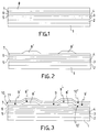
- a first layer of silicon dioxide 2 with a thickness d 2 and a refraction index n 2 is thermally raised preferably on a silicon support substrate 1.
- this first layer can be also obtained not by rising but by means of any deposition technique known by those skilled in the field for the silicon integration.
- a first not doped silicon layer 3 having a refraction index n 3 and a thickness d 3 is deposited on the first dioxide layer 2.
- a second silicon dioxide layer 4 of a thickness d 4 and a refraction index n 4 is thus deposited on the first not doped silicon layer 3.
- a second silicon layer 5 having a refraction index n 5 and a thickness d 5 is deposited on the second silicon dioxide layer 4.
- a third silicon dioxide layer 6 having a refraction index n 6 and a thickness d 6 is deposited on the second silicon layer 5.
- This sequence can be repeated several times thus increasing the reflectivity of the lower mirror consisting of a variable number of pairs of silicon/silicon dioxide with a suitable thickness and a refraction index.
- a first electro-conductive layer 7 provided, according to the described example, with doped polysilicon (preferably, with a doping of the type N+) is deposited on this third silicon dioxide layer 6.
- the doping may be obtained by doping the amorphous Si layer either in the deposition step or in a subsequent installation step.
- This material has a refraction index n 7 and is deposited until it reaches a thickness d 7 .
- a dielectric material layer 8 is then deposited on the doped polysilicon layer 7, as a passivation silicon oxide, i.e. having the function of an electric insulator between portions of the device.
- This passivation layer 8 (having, for example, a thickness of 10000 ⁇ ) is known to skilled operators, in other applications, as VAPOX when it is obtained by means of a chemical vapor deposition.
- a VAPOX layer being chemically vapor deposited has a large amount of hydrogen therein which is, advantageously, ejected by means of densification, i.e. a heat treatment at about 1100°C for a period of about 60 minutes.
- a typical photolithographic process is then carried out (comprising a first defining step for a photomask and a second photo-wet etching step) in order to obtain a dielectric region 8' from the dielectric layer VAPOX 8, as illustrated in the example from Fig. 2, of a toroidal base (this characteristic is not visible from the figure) and a substantially trapezoidal section.
- the substantially trapezoidal section is due to the use of a wet etching, and hence isotropic, allowing tilted walls to be engraved.
- the main function of the dielectric region 8' will be discussed while describing the operation mode of the device 100, the manufacturing method of which is being described.
- a secondary function of the dielectric region 8' is the insulation of the device 100 from other optoelectronic devices which can be integrated on the same substrate 1.
- a deposition step of an active means layer 10 having a first surface 10' and a second surface 10", being opposite to the first one, which morphologically follows the contour of the structure illustrated in Fig. 2 is then carried out.
- the first surface 10' is in contact with the first electro-conductive layer 7, in a side region 9' and in a first region 9, being substantially defined within the dielectric region 8', and in contact with the dielectric region 8' in a second region 8".
- the active means layer 10 has a refraction index n 10 and is deposited until it reaches a thickness d 10 .
- the active means layer which can be used, besides the already mentioned SRO, may be silicon dioxide doped with rare earths such as, for example, Terbium (Tb), Ytterbium (Yb) or Erbium (Eb).
- rare earths such as, for example, Terbium (Tb), Ytterbium (Yb) or Erbium (Eb).
- Tb Terbium
- Yb Ytterbium
- Eb Erbium
- a second electro-conductive layer 11 manufactured, for example, from doped polysilicon N+, is then deposited above the second surface 10" of the active means layer 10.
- This material has a refraction index n 11 and is deposited until it reaches a thickness d 11 .
- the two polysilicon layers may also have a different doping to which respective refraction indexes and respective thicknesses correspond.
- the doping of one of the two polysilicon layers can be also of the type P+. It is important that at least one of the two polysilicon layers 7 and 11 should be obtained by a doping of the type N+.
- a fourth silicon dioxide layer 12, having a refraction index n 12 and a thickness d 12 is deposited on the second doped polysilicon layer 11.
- a third non-doped silicon layer 13 having a refraction index n 13 and a thickness d 13 is deposited on this fourth silicon dioxide layer 12.
- the deposition sequence can be repeated, thus obtaining a mirror with a suitable reflectivity, with regard to the applications of interest, and in any case with a reflectivity which is lower than the one of the lower mirror, the manufacturing of which has been described above.
- the deposition of a passivation oxide layer is provided on the latter, as it will be described herein below.
- a typical photolithographic process comprising a first defining step for a photomask and a second photo-dry etching step for removing side portions of the layers 12 and 13 thus leaving a first multi-layer structure 16 unchanged being formed by the pile of said layers substantially aligned with the first region 9 and part of the dielectric region 8' is followed (figure 5).
- the use of a dry etching of the anisotropic type allows the multi-layer structure to be defined by substantially vertical sidewalls.
- a photolithographic process is then carried out in which a photomask is defined and a photo-dry etching is carried out so as to remove further side portions of the layers 10 and 11 in order to obtain a second multi-layer structure 17 formed by the pile of said layers aligned with almost all the whole part of the dielectric region 8" and more extended relative to the first multi-layer structure 16, such as illustrated in Fig. 6.
- a subsequent photolithographic process comprises the definition of a photomask the contour of which exposes the first polysilicon layer 7 to a dry etching step, following which peripheral portions of the first layer 7 are removed, thus obtaining the shape shown in Fig. 7 leaving a peripheral portion of the layer 6 uncovered.
- a fifth oxide layer 19 forming a passivation layer having a refraction index n 19 and a thickness d 19 is deposited on the structure from Fig. 7.
- This layer has the function of a passivation layer and is a part of the upper mirror.
- An annealing step at a temperature ranging between 750°C and 1100°C or, alternatively, a rapid thermal annealing (RTA) step is then followed in order to activate the polysilicon doping at a temperature of about 1000°C for a period of about 60 seconds.
- RTA rapid thermal annealing
- the selection of the heat treatment which needs to be used between the two of them depends on the desired active means to be activated. For example, in the case of SRO, an annealing at 1100°C is carried out.
- a first groove 19' and a second groove 19" are engraved in the oxide layer 19, for example simultaneously, by means of a single photolithographic process, due to the thickness uniformity of the layer 19.
- the first groove 19' extends in depth up to the first polysilicon layer 7 and is, for example, outside the dielectric region 8', thus surrounding the latter.
- the second groove 19" extends in depth up to the second non-doped polysilicon layer 11, thus surrounding the first multi-layer structure 16, such as shown in Fig. 9.
- a deposition step of electro-conductive material such as, for example, a metallization 20 is provided.
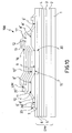
- Fig. 10 shows the structure of the RCLED device 100 obtained by means of the "Si-based technology" method described above.
- the substrate 1 is the support of the device 100, whereas the first silicon dioxide layer 2 may preferably have such characteristics as to insulate the same device from the substrate 1.
- the layers 2 to 7 provide a multi-layer lower mirror DM comprising a plurality of pairs of silicon-silicon dioxide layers, Si-SiO 2 , such as, for example, the layer pairs 2-3, 4-5, 6-7.
- the layers 11, 12, 13 and 19 provide a multi-layer upper mirror UM comprising a plurality of pairs of silicon-silicon dioxide layers, such as, for example, the layer pair 11-12 and, in the provided cases, the pair 13-19, or 11-19, for low-reflectivity mirrors.
- the two lower DM and upper UM mirrors, each of which including at least a dioxide layer, are dielectric mirrors.
- the active means layer 10 included between the lower mirror DM and the upper mirror UM defines a resonant cavity for the device 100 suitable to resonate at the emission wavelength ⁇ 0 .
- the two upper UM and lower DM mirrors have different reflectivities.
- the upper mirror UM from which the optical radiation output is provided has a reflectivity which is lower than the one of the other mirror.
- the lower mirror DM has a nominal reflectivity of 99-100% whereas the upper mirror UM has a reflectivity of 90% thus allowing the optical radiation reflecting through the latter to be transmitted of about 10%.
- the different reflectivity of the two mirrors can be obtained by manufacturing them with a different number of pairs of silicon-silicon dioxide.
- the lower mirror DM comprises two pairs whereas the upper mirror UM comprises a single pair.
- the number of layers for each of the mirrors can be increased.
- the number of these pairs of silicon-silicon dioxide will be suitably fixed according to the device applications and based on the specifications thereof such as, for example, length, directivity, monochromatic aspect of the light beam.
- both the mirrors UM and DM can be provided comprising more than one pair of silicon-silicon dioxide layers it is also possible, as in the described example, that one or both the mirrors may include a single pair of silicon-silicon dioxide layers.
- the passivation layer may have such characteristics as to be considered as comprised in the upper mirror UM and yet maintaining the function of a layer for insulating and starting the definition of the electric contacts.
- the passivation oxide layer 19 has such a refraction index n 19 and layer thickness d 19 as that the relation (2) is valid.
- one of the mirrors may further include a single pair of silicon-silicon dioxide layers in which the silicon dioxide layer is the same layer providing the passivation, such as the passivation oxide layer 19 and the polysilicon layer 11 provides the plate. Therefore, in this embodiment the second polysilicon layer 11 has the double function of a conductive layer and a first layer for a dielectric mirror.
- the Si-based technology is particularly advantageous because it allows mirrors with a high reflectivity to be obtained by using a limited number of pairs Si-SiO 2 . This is due to the fact that the pair Si-SiO 2 has a high jump in the refraction index between the two layers and hence a high reflectivity.
- the silicon nitride can be used in the place of the silicon dioxide, thus obtaining one or more pairs of silicon-silicon nitride.
- the observance of the relations (1) and (2) entails that for the radiation generated by the active means having the emission wavelength ⁇ 0 there is a constructive interference among the beam being reflected at each interface among adjacent layers having a different refraction index. For any wavelength different from ⁇ 0 the beams suffer a destructive interference ad hence they do not substantially allow that the optical radiation emitted by the active means of the device 100 can be detected outside the latter.
- the first 7 and second 11 electro-conductive layers allow to apply a pumping electric signal which can be supplied thereto by means of the first 20' and second 20" metallic regions of the metallization 20 to the active means layer 10, due to their electrical conductivity characteristics.
- first 7 and second 11 electro-conductive layers are obtained by a doping increasing the electrical conductivity thereof and are suitable to originate, if provided with an electric signal, a mutual current passage to which the generation of a respective electric field, the field lines of which substantially have a direction that is transversal to the plane of the two layers 7 and 11, corresponds.
- the first layer 7 and the second layer 11 being electro-conductive can be defined as electrical plates being opposite to each other and separate from the active means layer 10 in which the propagation of a substantially uniform electric occurs.
- a non-sufficient doping of the two conductive layers 7 and 11 entails a non-uniform propagation of the electric field between the two plates.
- a recommended doping is, for example, higher than 10 17 cm -3 .
- the dielectric region 8' increases the distance between the first 7 and second 11 electro-conductive layers.
- the first 7 and second 11 electro-conductive layers are separated at the second region 8" and hence they are spaced from the dielectric region 8' and the active means layer 10.
- the first 7 and second 11 electro-conductive layers are only separated by the active means layer 10, thus being closer to each other compared to what may occur at the second region 8". Accordingly, under the same voltage applied to the first 7 and second 11 electro-conductive layers the electric field, in the portion of the active means layer 10 corresponding to the first region 9, is higher than the one located at the second region 8". Therefore, the generation of an electric current (i.e.
- an electron passage) for exciting the same active means is facilitated in this portion of the active means layer directly facing the first 7 and second 11 electro-conductive layers.
- the dielectric region 8' allows the force lines of the electric field to be conveyed outside the dielectric region 8' and hence to the first region 9.
- the portion of the active means layer 10 corresponding to the first region 9 defines a main area generating the radiation, indicated in the figures with a dashed contour and a reference number 30.
- first 7 and second 11 electro-conductive layers have such particular optical characteristics as to ensure the required constructive interference to the upper and lower mirrors.
- the first multi-layer structure 16 has a sufficient width suitable to ensure that the main radiation area 30 is entirely included between the upper mirror UM and the lower mirror DM.
- n 10 ⁇ d 10 m ⁇ ⁇ 0 / 2 wherein m is an integral and positive numerical value.
- the active means layer 10 being in contact with the polysilicon layers 7 and 11 (which are, in turn, in contact with the mirrors DM and UM), changes the distribution of the energy bands of the layers included in the resonant cavity.
- the active means layer 10 causes a discontinuity, i.e. a fault in the resonant cavity energy band, due to which a decrease in the reflectivity of the mirrors UM and DM estimated at the wavelength ⁇ 0 occurs.
- the first 20' and second 20" metallic regions defined during the metallization process 20 have the function of electric contacts allowing the active means layer 10 to be supplied with the pumping electric signal being suitably generated.
- the first metallic region 20' is in contact with the first electro-conductive layer 7 whereas the second metallic region 20" is in contact with the second electro-conductive layer 11.
- Both the first 20' and second 20" have, for example, an annular base, and more precisely the ring of the first metallic region 20' is outer than the one of the second metallic region 20".
- the pumping electric signal is, preferably, either a continuous or alternating potential difference (PD) applied to the first 7 and second 11 electro-conductive layers which entails a passage of the electric current and a generation of a corresponding substantially uniform electric field in the active means layer 10, i.e. with field lines being substantially transversal to the plane defined by the two layers 7 and 11.
- Typical values of this potential difference are 25-30 V or 50-60 V, as a result of the type of application and the type of device used and the type of active means.
- the pumping current electrons collide with the nanocrystals provided in the active means 10 thus generating electron-hole pairs which emit photons by recombining with one another in the nanocrystal, i.e. optical radiation.
- the generated optical radiation is spread within the cavity defined by the upper mirror UM and the lower mirror DM substantially at the main radiation area 30. Following these reflections within the cavity, destructive interferences and constructive interferences bringing to the selection of the radiation with the wavelength ⁇ 0 occur.
- a part of this radiation leaks from the upper mirror UM in the form of a beam passing through the portion of the passivation oxide layer 19 facing the radiation area 30 being substantially orthogonal to the latter.
- the presence of the resonant cavity allows a selected wavelength ⁇ 0 and high-directivity optical radiation to be obtained.
- the RCLED device 100 has a high-efficiency emission, due to the electric pumping directly on the active means layer 10.
- the invention described above can be also implemented for manufacturing a device of the VCSEL type which, as already said above, is a laser source.
- This VCSEL device can be structurally similar to the one described above and shown in Fig. 10, unless the active means layer 10 is such as to provide an optical population inversion subsequent to an electric pumping. In this case, the number of the pairs providing the dielectric mirrors requires to be suitably examined such as to obtain a suitable Q-factor.
- active means which are assumed to be suitable to give rise to a population inversion are either SRO doped with Erbium or a MQW comprising nanometric Si-SiO 2 layers.
- An active means including SRO doped with erbium is described in the article by M.E. Castagna et al. mentioned above.
- SRO is doped with Erbium
- the SRO nanocrystals are excited by the collision of hot electrons.
- the nanostructure exciting time is of some ⁇ s.
- the excitation is thus transferred to the level I 11/2 of the Erbium ion near the nanostructure, and hence the I 13/2 level forming the metastable level with a decay time in the order of the ms, is excited by means of a rapid decay. Therefore, a population inversion occurs between the I 13/2 level and the I 15/2 level, which is the basic level for the Er ion.
- the VCSEL of the known type using layers of materials of the III-V group as an active means are also called quantum cascade lasers.
- the MQW is included with nanometric layers of SiO 2 and Si being doped degenerate N+ (conduction band Fermi level).
- N+ conduction band Fermi level
- the device 100 in accordance with the invention (both of the RCLED type, and the VCSEL type) is particularly suitable for applications in the optical interconnections as an optical radiation source to be launched, for example, in optical waveguides either of the integrate or fiber technology type.
- the device of the invention can be employed for generating electromagnetic radiations with wavelengths ranging between 540 nm and 980 nm or 1540 nm.
- the RCLED device can be employed, for example, in applications of the IrDA type (Infrared Data Association), i.e. in the infrared communications in which, for example, an emission wavelength may be 850 nm.
- IrDA Infrared Data Association
- the most important required characteristics are the absolute power, the total efficiency and the low costs.
- the width of the emission spectrum and the luminosity are less important characteristics.
- a resonant cavity is useful to be preferably provided with so-called low-reflectivity upper mirrors. In order to obtain this decrease in the reflectivity, the number of layers included in the upper mirror requires to be reduced.
- the upper mirror UM instead of consisting of such pairs of silicon-silicon dioxide as to ensure even a reflectivity of 98%, consists of a single polysilicon layer, for example the first doped polysilicon layer N+ 7, for pumping the active means, whereas the silicon dioxide layer may be the coating oxide layer, for example the passivation layer 19.
- a device 200 similar to the one 100 described above but obtained by a different method is shown.
- the embodiment from Fig. 11 shows by way of example the case where the upper mirror UM comprises a single pair of layers such as the second polysilicon layer 11 and the passivation oxide layer 19.
- the device 200 from Fig. 11 is provided with a region 80' for insulating and defining the active area (i.e. the flat region taken up by the active means 10) obtained in a manner which is different from the one 8' from Fig. 10, instead of the oxide region 8' of the device 100.
- the active means layer 10 is provided by being arranged above the first layer 7, after the first polysilicon layer 7 has been formed.
- the active means used is, preferably, SRO, i.e. silicon oxide having an excess of silicon.
- a silicon nitride protective layer (not shown in the figure) is formed above a part of the free surface of the active means 10. Particularly, this silicon nitride layer is arranged above a central area of the active means 10 so as to protect the part of the active means which will be involved in the generation of the optical radiation.
- the dielectric defining the active area is obtained by subjecting the active means layer 10 to an oxidation process being carried out at such a temperature and period as to allow the substantially total oxidation of the exceeding silicon, but without oxidizing the first doped polysilicon layer 7 situated on the lower mirror DM.
- a stoichiometric oxide region (without exceeding silicon) 80' is increased in the nitride non-protected areas to the detriment of the exceeding silicon being found in the SRO layer, which is typically nearly around 40%.
- This oxidation technique is commonly employed for forming the so-called isolating LOCOS (LOCal Oxidation of Silicon) within the scope of the Si-based technology.
- the SRO active means 10 (shown in Fig. 11 with black dots), only takes up the central region and is defined by the stoichiometric oxide 80'. It shall be noted that due to the oxidation process the stoichiometric oxide 80' increases in thickness relative to the SRO active means 10, thus being in any case connected to the latter by slight sloping walls.
- the stoichiometric oxide 80' is a dielectric region having a function which is similar to the one of the dielectric region 8' described with reference to the device 100.
- This method is particularly advantageous because it allows a structure (being formed by the active means 10 and the insulating region 80') having an only slightly corrugated shape to be obtained. This allows the subsequent layers of the device 200 to be deposited on this structure so that they have substantially uniform thicknesses. Moreover, the use of the oxidation process reduces the number of the processing steps of the photolithographic type.
- the electric field lines are much thicker at the active means 10, because the latter, on the other hand, has a lower thickness and breakdown.
- the proposed device and its respective method for manufacturing are suitable to solve the object of the present invention.
- the conveying of the electric field to the main radiation area 30, which can be carried out due to the presence of the dielectric region 8', allows to reduce the passage of the electric current 8 associated to the electric field and hence to reduce the generation of optical radiation between portions of the plates not facing the upper mirror UM.
- the optical radiation generated in portions of the active means layer 10 not facing the upper mirror UM is disadvantageous. In fact, this radiation does not suffer from the suitable reflections within the resonant cavity, thus causing an emission of optical radiation to the outside, having characteristics which are different from the one emitted at the main area 30.
- the use of the dielectric region 8' (similarly to the one 80') allows a particularly uniform optical radiation generation and emission in terms of power, wavelength and spectrum width to be obtained in the main area 30.
- the shape of the first rib 16 and the shape of the second electro-conductive layer 7 cause the interaction between the two plates to be reduced to a minimum outside the dielectric region 8' so as to have electric field lines which are insignificant relative to the main radiation area 30. This allows to reduce the possible occurrence of the resonance of the device due to the interaction between the first and second metallic regions in the case where an electric field is present outside the dielectric region 8'. Similar remarks are also valid for the device 200 from Fig. 11.
Landscapes
- Semiconductor Lasers (AREA)
Priority Applications (2)
| Application Number | Priority Date | Filing Date | Title |
|---|---|---|---|
| EP05425430.5A EP1734591B1 (fr) | 2005-06-16 | 2005-06-16 | Dispositif émetteur de rayonnement optique et procédé de manufacture d'un tel dispositif |
| US11/422,264 US7829904B2 (en) | 2005-06-16 | 2006-06-05 | Optical radiation emitting device and method of manufacturing same |
Applications Claiming Priority (1)
| Application Number | Priority Date | Filing Date | Title |
|---|---|---|---|
| EP05425430.5A EP1734591B1 (fr) | 2005-06-16 | 2005-06-16 | Dispositif émetteur de rayonnement optique et procédé de manufacture d'un tel dispositif |
Publications (2)
| Publication Number | Publication Date |
|---|---|
| EP1734591A1 true EP1734591A1 (fr) | 2006-12-20 |
| EP1734591B1 EP1734591B1 (fr) | 2013-05-22 |
Family
ID=35262140
Family Applications (1)
| Application Number | Title | Priority Date | Filing Date |
|---|---|---|---|
| EP05425430.5A Expired - Lifetime EP1734591B1 (fr) | 2005-06-16 | 2005-06-16 | Dispositif émetteur de rayonnement optique et procédé de manufacture d'un tel dispositif |
Country Status (2)
| Country | Link |
|---|---|
| US (1) | US7829904B2 (fr) |
| EP (1) | EP1734591B1 (fr) |
Cited By (3)
| Publication number | Priority date | Publication date | Assignee | Title |
|---|---|---|---|---|
| ITTO20080781A1 (it) * | 2008-10-23 | 2010-04-24 | St Microelectronics Srl | Dispositivo emettitore di radiazione ottica a cavita' risonante e processo di fabbricazione del dispositivo |
| ITTO20080941A1 (it) * | 2008-12-17 | 2010-06-18 | St Microelectronics Srl | Procedimento di fabbricazione di un dispositivo emettitore di radiazione ottica a cavita' risonante |
| JP2011135031A (ja) * | 2009-11-26 | 2011-07-07 | Ricoh Co Ltd | 面発光レーザ素子、面発光レーザアレイ、光走査装置及び画像形成装置 |
Families Citing this family (7)
| Publication number | Priority date | Publication date | Assignee | Title |
|---|---|---|---|---|
| JP5515767B2 (ja) * | 2009-05-28 | 2014-06-11 | 株式会社リコー | 面発光レーザ素子の製造方法、面発光レーザ素子、面発光レーザアレイ、光走査装置及び画像形成装置 |
| US8106421B2 (en) * | 2009-08-21 | 2012-01-31 | University Of Seoul Industry Cooperation Foundation | Photovoltaic devices |
| IT1396818B1 (it) * | 2009-11-19 | 2012-12-14 | St Microelectronics Srl | Dispositivo elettroluminescente pompabile elettricamente ad emissione laterale, integrato in una guida d'onda passiva per generare luce o amplificare un segnale e procedimento di fabbricazione. |
| US9256027B2 (en) | 2012-07-02 | 2016-02-09 | Stmicroelectronics S.R.L. | Integrated optoelectronic device and system with waveguide and manufacturing process thereof |
| ITTO20120583A1 (it) | 2012-07-02 | 2014-01-03 | St Microelectronics Srl | Dispositivo optoelettronico integrato con guida d'onda e relativo procedimento di fabbricazione |
| TWI540753B (zh) * | 2013-07-30 | 2016-07-01 | 隆達電子股份有限公司 | 發光二極體結構 |
| US10132934B2 (en) | 2014-09-17 | 2018-11-20 | Stmicroelectronics S.R.L. | Integrated detection device, in particular detector of particles such as particulates or alpha particles |
Citations (6)
| Publication number | Priority date | Publication date | Assignee | Title |
|---|---|---|---|---|
| US5493577A (en) | 1994-12-21 | 1996-02-20 | Sandia Corporation | Efficient semiconductor light-emitting device and method |
| US5726462A (en) * | 1996-02-07 | 1998-03-10 | Sandia Corporation | Semiconductor structures having electrically insulating and conducting portions formed from an AlSb-alloy layer |
| US5818863A (en) * | 1996-01-30 | 1998-10-06 | France Telecom | Laser-emitting component having an injection zone of limited width |
| US5848086A (en) * | 1996-12-09 | 1998-12-08 | Motorola, Inc. | Electrically confined VCSEL |
| US5877509A (en) | 1997-11-14 | 1999-03-02 | Stanford University | Quantum well exciton-polariton light emitting diode |
| US20030209714A1 (en) | 2000-10-12 | 2003-11-13 | General Electric Company | Solid state lighting device with reduced form factor including led with directional emission and package with microoptics |
Family Cites Families (10)
| Publication number | Priority date | Publication date | Assignee | Title |
|---|---|---|---|---|
| US5724374A (en) * | 1996-08-19 | 1998-03-03 | Picolight Incorporated | Aperture comprising an oxidized region and a semiconductor material |
| US6075804A (en) * | 1998-01-28 | 2000-06-13 | Picolight Incorporated | Semiconductor device having an oxide defined aperture |
| JPH11307882A (ja) * | 1998-02-17 | 1999-11-05 | Fuji Xerox Co Ltd | 面発光型半導体レ―ザ、面発光型半導体レ―ザアレイ、及び面発光型半導体レ―ザの製造方法 |
| US6556607B1 (en) * | 2000-06-23 | 2003-04-29 | Picolight, Incorporated | Temperature compensated lasers |
| US6639932B1 (en) * | 2001-03-16 | 2003-10-28 | Coretek, Inc. | Vertical-cavity surface-emitting laser (VCSEL) with cavity compensated gain |
| US20020150130A1 (en) * | 2001-04-16 | 2002-10-17 | Coldren Larry A. | Tunable VCSEL assembly |
| WO2005029655A2 (fr) * | 2003-09-18 | 2005-03-31 | Nanosource Inc. | Laser a cavite verticale emettant par la surface (vcsel) confine en mode epitaxial et procede de production associe |
| JP4602692B2 (ja) * | 2004-04-23 | 2010-12-22 | 株式会社リコー | 面発光レーザ及び光伝送システム |
| ITTO20080781A1 (it) * | 2008-10-23 | 2010-04-24 | St Microelectronics Srl | Dispositivo emettitore di radiazione ottica a cavita' risonante e processo di fabbricazione del dispositivo |
| IT1395244B1 (it) * | 2008-12-17 | 2012-09-05 | St Microelectronics Srl | Procedimento di fabbricazione di un dispositivo emettitore di radiazione ottica a cavita' risonante |
-
2005
- 2005-06-16 EP EP05425430.5A patent/EP1734591B1/fr not_active Expired - Lifetime
-
2006
- 2006-06-05 US US11/422,264 patent/US7829904B2/en not_active Expired - Fee Related
Patent Citations (6)
| Publication number | Priority date | Publication date | Assignee | Title |
|---|---|---|---|---|
| US5493577A (en) | 1994-12-21 | 1996-02-20 | Sandia Corporation | Efficient semiconductor light-emitting device and method |
| US5818863A (en) * | 1996-01-30 | 1998-10-06 | France Telecom | Laser-emitting component having an injection zone of limited width |
| US5726462A (en) * | 1996-02-07 | 1998-03-10 | Sandia Corporation | Semiconductor structures having electrically insulating and conducting portions formed from an AlSb-alloy layer |
| US5848086A (en) * | 1996-12-09 | 1998-12-08 | Motorola, Inc. | Electrically confined VCSEL |
| US5877509A (en) | 1997-11-14 | 1999-03-02 | Stanford University | Quantum well exciton-polariton light emitting diode |
| US20030209714A1 (en) | 2000-10-12 | 2003-11-13 | General Electric Company | Solid state lighting device with reduced form factor including led with directional emission and package with microoptics |
Non-Patent Citations (1)
| Title |
|---|
| CASTAGNA M E ET AL: "Si-based resonant cavity light-emitting devices", PROCEEDINGS OF THE SPIE - THE INTERNATIONAL SOCIETY FOR OPTICAL ENGINEERING SPIE-INT. SOC. OPT. ENG USA, vol. 5366, no. 1, 2004, pages 26 - 35, XP002354134, ISSN: 0277-786X * |
Cited By (4)
| Publication number | Priority date | Publication date | Assignee | Title |
|---|---|---|---|---|
| ITTO20080781A1 (it) * | 2008-10-23 | 2010-04-24 | St Microelectronics Srl | Dispositivo emettitore di radiazione ottica a cavita' risonante e processo di fabbricazione del dispositivo |
| US8981400B2 (en) | 2008-10-23 | 2015-03-17 | Stmicroelectronics S.R.L. | Resonant cavity optical radiation emission device and process for manufacturing same |
| ITTO20080941A1 (it) * | 2008-12-17 | 2010-06-18 | St Microelectronics Srl | Procedimento di fabbricazione di un dispositivo emettitore di radiazione ottica a cavita' risonante |
| JP2011135031A (ja) * | 2009-11-26 | 2011-07-07 | Ricoh Co Ltd | 面発光レーザ素子、面発光レーザアレイ、光走査装置及び画像形成装置 |
Also Published As
| Publication number | Publication date |
|---|---|
| US20060284200A1 (en) | 2006-12-21 |
| US7829904B2 (en) | 2010-11-09 |
| EP1734591B1 (fr) | 2013-05-22 |
Similar Documents
| Publication | Publication Date | Title |
|---|---|---|
| US8111729B2 (en) | Multi-wavelength hybrid silicon laser array | |
| Deppe et al. | Low-threshold vertical-cavity surface-emitting lasers based on oxide-confinement and high contrast distributed Bragg reflectors | |
| US6697403B2 (en) | Light-emitting device and light-emitting apparatus using the same | |
| EP1734591B1 (fr) | Dispositif émetteur de rayonnement optique et procédé de manufacture d'un tel dispositif | |
| US7809039B2 (en) | Light-emitting device and manufacturing method of the same | |
| US7645626B2 (en) | Multiple GaInNAs quantum wells for high power applications | |
| JP2002504754A (ja) | 光送信機及び光受信機を有するコンポーネント | |
| US9450375B2 (en) | High-power diode laser and method for producing a high-power diode laser | |
| CN101809832A (zh) | 光电子器件 | |
| US20080014667A1 (en) | Modifying the optical properties of a nitride optoelectronic device | |
| US7006545B2 (en) | Semiconductor laser device and optical fiber amplifier using the same | |
| Major Jr et al. | High power, high efficiency antiguide laser arrays | |
| US6542527B1 (en) | Vertical cavity surface emitting laser | |
| CN121035762B (zh) | 一种低发散角窄线宽高功率半导体激光器 | |
| CN111342341B (zh) | 一种激光器结构及其制备方法和应用 | |
| US7151282B2 (en) | Light emitting diode | |
| US20100014549A1 (en) | Surface Emitting Semiconductor Body with Vertical Emission Direction and Stabilized Emission Wavelength | |
| US20100151603A1 (en) | Method of manufacturing a resonant cavity optical radiation emitting device | |
| Coffa et al. | Feasibility analysis of laser action in erbium-doped silicon waveguides | |
| US8981400B2 (en) | Resonant cavity optical radiation emission device and process for manufacturing same | |
| US7778300B2 (en) | Optically pumped semiconductor device | |
| Joyner et al. | A multifrequency waveguide grating laser by selective area epitaxy | |
| Steckl et al. | GaAs quantum well distributed Bragg reflection laser with AlGaAs/GaAs superlattice gratings fabricated by focused ion beam mixing | |
| US11228160B2 (en) | AlGaInPAs-based semiconductor laser device and method for producing same | |
| TWI818580B (zh) | 半導體元件的製造方法 |
Legal Events
| Date | Code | Title | Description |
|---|---|---|---|
| PUAI | Public reference made under article 153(3) epc to a published international application that has entered the european phase |
Free format text: ORIGINAL CODE: 0009012 |
|
| AK | Designated contracting states |
Kind code of ref document: A1 Designated state(s): AT BE BG CH CY CZ DE DK EE ES FI FR GB GR HU IE IS IT LI LT LU MC NL PL PT RO SE SI SK TR |
|
| AX | Request for extension of the european patent |
Extension state: AL BA HR LV MK YU |
|
| RIN1 | Information on inventor provided before grant (corrected) |
Inventor name: MONACO, MARIANTONIETTA Inventor name: MUSCARA', ANNA Inventor name: CASTAGNA, MARIA Inventor name: COFFA, SALVATORE |
|
| 17P | Request for examination filed |
Effective date: 20070531 |
|
| AKX | Designation fees paid |
Designated state(s): DE FR GB IT |
|
| 17Q | First examination report despatched |
Effective date: 20071121 |
|
| RAP1 | Party data changed (applicant data changed or rights of an application transferred) |
Owner name: STMICROELECTRONICS SRL |
|
| RAP1 | Party data changed (applicant data changed or rights of an application transferred) |
Owner name: STMICROELECTRONICS SRL |
|
| REG | Reference to a national code |
Ref country code: DE Ref legal event code: R079 Ref document number: 602005039674 Country of ref document: DE Free format text: PREVIOUS MAIN CLASS: H01L0033000000 Ipc: H01L0033140000 |
|
| GRAP | Despatch of communication of intention to grant a patent |
Free format text: ORIGINAL CODE: EPIDOSNIGR1 |
|
| RIC1 | Information provided on ipc code assigned before grant |
Ipc: H01L 33/14 20100101AFI20121005BHEP Ipc: H01L 33/46 20100101ALI20121005BHEP Ipc: H01L 33/10 20100101ALI20121005BHEP |
|
| GRAS | Grant fee paid |
Free format text: ORIGINAL CODE: EPIDOSNIGR3 |
|
| GRAA | (expected) grant |
Free format text: ORIGINAL CODE: 0009210 |
|
| RIN1 | Information on inventor provided before grant (corrected) |
Inventor name: MUSCARA', ANNA Inventor name: MONACO, MARIANTONIETTA Inventor name: COFFA, SALVATORE Inventor name: CASTAGNA, MARIA |
|
| AK | Designated contracting states |
Kind code of ref document: B1 Designated state(s): DE FR GB IT |
|
| RAP1 | Party data changed (applicant data changed or rights of an application transferred) |
Owner name: STMICROELECTRONICS S.R.L. |
|
| REG | Reference to a national code |
Ref country code: GB Ref legal event code: FG4D |
|
| RIN1 | Information on inventor provided before grant (corrected) |
Inventor name: COFFA, SALVATORE Inventor name: MONACO, MARIANTONIETTA Inventor name: CASTAGNA, MARIA Inventor name: MUSCARA', ANNA |
|
| REG | Reference to a national code |
Ref country code: DE Ref legal event code: R096 Ref document number: 602005039674 Country of ref document: DE Effective date: 20130718 |
|
| PGFP | Annual fee paid to national office [announced via postgrant information from national office to epo] |
Ref country code: DE Payment date: 20130627 Year of fee payment: 9 |
|
| PG25 | Lapsed in a contracting state [announced via postgrant information from national office to epo] |
Ref country code: IT Free format text: LAPSE BECAUSE OF FAILURE TO SUBMIT A TRANSLATION OF THE DESCRIPTION OR TO PAY THE FEE WITHIN THE PRESCRIBED TIME-LIMIT Effective date: 20130522 |
|
| PLBE | No opposition filed within time limit |
Free format text: ORIGINAL CODE: 0009261 |
|
| REG | Reference to a national code |
Ref country code: FR Ref legal event code: ST Effective date: 20140228 |
|
| STAA | Information on the status of an ep patent application or granted ep patent |
Free format text: STATUS: NO OPPOSITION FILED WITHIN TIME LIMIT |
|
| GBPC | Gb: european patent ceased through non-payment of renewal fee |
Effective date: 20130822 |
|
| 26N | No opposition filed |
Effective date: 20140225 |
|
| PG25 | Lapsed in a contracting state [announced via postgrant information from national office to epo] |
Ref country code: FR Free format text: LAPSE BECAUSE OF NON-PAYMENT OF DUE FEES Effective date: 20130722 |
|
| REG | Reference to a national code |
Ref country code: DE Ref legal event code: R097 Ref document number: 602005039674 Country of ref document: DE Effective date: 20140225 |
|
| PG25 | Lapsed in a contracting state [announced via postgrant information from national office to epo] |
Ref country code: GB Free format text: LAPSE BECAUSE OF NON-PAYMENT OF DUE FEES Effective date: 20130822 |
|
| REG | Reference to a national code |
Ref country code: DE Ref legal event code: R119 Ref document number: 602005039674 Country of ref document: DE |
|
| REG | Reference to a national code |
Ref country code: DE Ref legal event code: R119 Ref document number: 602005039674 Country of ref document: DE Effective date: 20150101 |
|
| PG25 | Lapsed in a contracting state [announced via postgrant information from national office to epo] |
Ref country code: DE Free format text: LAPSE BECAUSE OF NON-PAYMENT OF DUE FEES Effective date: 20150101 |