EP1733362B1 - Cooking range - Google Patents
Cooking range Download PDFInfo
- Publication number
- EP1733362B1 EP1733362B1 EP05726080.4A EP05726080A EP1733362B1 EP 1733362 B1 EP1733362 B1 EP 1733362B1 EP 05726080 A EP05726080 A EP 05726080A EP 1733362 B1 EP1733362 B1 EP 1733362B1
- Authority
- EP
- European Patent Office
- Prior art keywords
- user interface
- microprocessor
- exponential curve
- digital
- digitized
- Prior art date
- Legal status (The legal status is an assumption and is not a legal conclusion. Google has not performed a legal analysis and makes no representation as to the accuracy of the status listed.)
- Active
Links
Images


Classifications
-
- G—PHYSICS
- G08—SIGNALLING
- G08B—SIGNALLING OR CALLING SYSTEMS; ORDER TELEGRAPHS; ALARM SYSTEMS
- G08B5/00—Visible signalling systems, e.g. personal calling systems, remote indication of seats occupied
- G08B5/22—Visible signalling systems, e.g. personal calling systems, remote indication of seats occupied using electric transmission; using electromagnetic transmission
-
- F—MECHANICAL ENGINEERING; LIGHTING; HEATING; WEAPONS; BLASTING
- F24—HEATING; RANGES; VENTILATING
- F24C—DOMESTIC STOVES OR RANGES ; DETAILS OF DOMESTIC STOVES OR RANGES, OF GENERAL APPLICATION
- F24C7/00—Stoves or ranges heated by electric energy
- F24C7/08—Arrangement or mounting of control or safety devices
- F24C7/082—Arrangement or mounting of control or safety devices on ranges, e.g. control panels, illumination
- F24C7/085—Arrangement or mounting of control or safety devices on ranges, e.g. control panels, illumination on baking ovens
-
- F—MECHANICAL ENGINEERING; LIGHTING; HEATING; WEAPONS; BLASTING
- F24—HEATING; RANGES; VENTILATING
- F24C—DOMESTIC STOVES OR RANGES ; DETAILS OF DOMESTIC STOVES OR RANGES, OF GENERAL APPLICATION
- F24C7/00—Stoves or ranges heated by electric energy
- F24C7/08—Arrangement or mounting of control or safety devices
- F24C7/082—Arrangement or mounting of control or safety devices on ranges, e.g. control panels, illumination
- F24C7/086—Arrangement or mounting of control or safety devices on ranges, e.g. control panels, illumination touch control
-
- G—PHYSICS
- G08—SIGNALLING
- G08B—SIGNALLING OR CALLING SYSTEMS; ORDER TELEGRAPHS; ALARM SYSTEMS
- G08B5/00—Visible signalling systems, e.g. personal calling systems, remote indication of seats occupied
-
- H—ELECTRICITY
- H05—ELECTRIC TECHNIQUES NOT OTHERWISE PROVIDED FOR
- H05B—ELECTRIC HEATING; ELECTRIC LIGHT SOURCES NOT OTHERWISE PROVIDED FOR; CIRCUIT ARRANGEMENTS FOR ELECTRIC LIGHT SOURCES, IN GENERAL
- H05B6/00—Heating by electric, magnetic or electromagnetic fields
- H05B6/64—Heating using microwaves
- H05B6/6435—Aspects relating to the user interface of the microwave heating apparatus
-
- F—MECHANICAL ENGINEERING; LIGHTING; HEATING; WEAPONS; BLASTING
- F24—HEATING; RANGES; VENTILATING
- F24C—DOMESTIC STOVES OR RANGES ; DETAILS OF DOMESTIC STOVES OR RANGES, OF GENERAL APPLICATION
- F24C7/00—Stoves or ranges heated by electric energy
- F24C7/08—Arrangement or mounting of control or safety devices
- F24C7/082—Arrangement or mounting of control or safety devices on ranges, e.g. control panels, illumination
- F24C7/083—Arrangement or mounting of control or safety devices on ranges, e.g. control panels, illumination on tops, hot plates
Definitions
- the present invention relates to appliances and more particularly to an interactive informational interface display on ranges, stoves and other appliances.
- EP 1 272 007 discloses a display unit provided on a panel, displays a control for each burner of a cover, and a selector on the panel selects a power level for actuating the selected burner.
- a processor selectively actuates each of the burner, in response to sequential manipulation of the indicia, and deactivates the selectively actuated burner, in response to manipulation of either of the indicia.
- EP 1 203 914 discloses The operating and display unit has an operating and display field provided with touch-control elements for selection of individual cooking zones within the cooking field and operating elements for setting the cooking parameters, with a respective display associated with each touch-control element.
- the latter are arranged in 2 rows each containing 3 columns, with a further option position for a touch-control selection element or a touch-control setting element.
- WO 97/50168 discloses an apparatus for supplying regulated voltage d.c. electrical power to an LED array and includes a rectifier responsive to a.c power for generating rectified d.c. power and a power factor correcting and voltage regulating buck/boost switchmode converter responsive to the rectified d.c. power for generating regulated voltage d.c. power to illuminate the LED array.
- DE 44 14 825 discloses a food processor with a mixing vessel and a drive mechanism for an agitator in the mixing vessel, the lower region of which can be heated. As an improvement on a kitchen appliance of this type, it is proposed that the heating should be made dependent on the rate at which the temperature rises.
- US 6 255 960 discloses A system and method for allowing a user to program characteristics of at least one light emitting diode (LED) in order to convey information about the operational status of an appliance, such as a printer.
- the user of the printer selects one of a plurality of display mode options for the LED for a particular operational status condition of the printer. For each display mode option, there is a range of parameters that can be programmed by the user.
- Present invention provides a cooking range that has an informational display that disappears, at least partially, when not in use.
- a cooking range that includes: a user interface having a plurality of touch pad buttons further comprising an informational display area; a microprocessor-based fader electronic control system further comprising: a digitized exponential curve; a time-stepping algorithm to read data from the exponential curve; a pulse width modulated output signal generated by the microprocessor and controlled by the time-stepped algorithm; a digital to analog circuit driven by the pulse-width modulated output signal; an LED array located behind the user interface and driven by the digital to analog circuit; and, wherein the LED fader electronic control system receives an input from the user interface and further processes the information to reduce or increase at least a portion of the light intensity of the LED array.
- the method includes providing a user interface having a plurality of touch pad buttons and an informational display area, an electronic control system comprising a digitized exponential curve, a microprocessor based time-stepped algorithm to process data from the digitized exponential curve, a pulse width modulated out put digital signal generated by the microprocessor based on the data received from the time-stepped algorithm, a digital to analog circuit to receive the pulse width modulated output signal, and an at least one light-emitting diode; inputting a signal to the user interface; reading the digitized data from the digitized exponential curve; transmitting the data to the output of the microprocessor; modifying the frequency of the pulse-width modulated signal; transmitting the pulse-width modulated signal to the digital to analog circuit; applying a voltage to the output of the digital to analog circuit; and, adjusting the light intensity of the at least one light-emitting diode
- FIG. 1 shows a front view of a typical range 10 that incorporates a disappearing interface system in accordance with this invention.
- the present invention may be utilized on any other sort of device.
- the invention may be utilized on other types of appliances, such as large or small appliances.
- large appliances include washers, dryers, refrigerators, and freezers.
- small appliances includes, toasters, coffee makers, and microwave ovens.
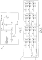
- FIG. 3 is a top level diagram showing communication between the user interface 12 and a light emitting diode (LED) fader electronic control system 30.
- the disappearing interface system consists of a user interface 12 and the LED fader electro nic control system
- the example user interface 12 further includes an informational display area 14 and black tinted glass 16.
- the example informational display area 14 displays touch sensitive areas 18 used for providing user input to operate the range 10.
- the user interface 12 communicates with the electronic control system of the range 10 to perform basic operations (e.g. cooking, baking, roasting, etc.) commonly known in the art and will not be further described herein.
- the example informational display area 14 also displays information providing areas, such as a clock 20, and other information such as oven temperature, minutes remaining until cooking is complete, etc.
- the touch sensitive areas 18 may have various constructions, configurations, and operation techniques.
- buttons For simplicity, the touch sensitive areas are simply referred to as "buttons.” However, it is to be appreciated that touch alone may be sufficient to effect operation and that physical movement of the buttons may not occur.
- the black tinted glass 16 is used to hide the components of the disappearing interface system when the disappearing interface system is inactive as will be described further below. In other words, the black tinted glass 16 will appear to be a plain black glass when the disappearing interface system is inactive as shown in FIG. 1 . Thus, a clear, uncluttered appearance is provided.
- the example LED fader electronic control system 30 is a microprocessor-based control system.
- an output from a digitized exponential curve 32 is provided to a microprocessor that performs the functions of a time -stepping algorithm 34, and providing a pulse width modulated (PWM) output signal 36.
- PWM pulse width modulated
- the PWM signal is provided to a digital to analog conversion circuit (D/A circuit) 38, whose output is provided to an LED array 40.
- D/A circuit digital to analog conversion circuit
- the microprocessor performs the time-stepping software routine that utilizes the digitized data from the digitized exponential curve 32 to generate the PWM output signal 36.
- the funct ion digitized exponential curve 36 may be provided by any suitable components(s), operations(s), etc. such as a provision of information from a memory or an algorithm being performed.
- the D/A circuit 38 in turn drives the light intensities of the LED light array 40.
- the intensity of the LED light array 40 is a function of the PWM signal 36 frequency generated by the microprocessor.
- the human eye detects magnitude of light in a nonlinear manner.
- a nonlinear fading effect is utilized to give the appearance that the LED light array 40 has a changing (e.g., increase or decrease) intensity in a smooth linear fashion.
- the digitized exponential curve 32 such as the one shown in FIG. 5 , provides this effect.
- the exponential curve of FIG. 5 is for purposes of illustration only and is not intended to limit the scope of the invention. Any type of table, equation, graph etc. depicting a rate of increase or decrease such as a linear rate, exponential rate, logarithmic rate, etc. can be used in the present invention.
- any time interval or exponential rate can be used in the present invention. As the time increases from 0 seconds to 4 seconds the corresponding normalized count value increases at an exponential rate of x 3 .
- the digitized exponential curve 32 itself, is an indication of the increase or decrease in light intensity of the LED array 40.
- the time-stepping algorithm 34 reads the data from the digitized exponential curve 32 (e.g., FIG. 5 ) and provides information for use in providing the PWM signal 36 output by the microprocessor. The time-stepping algorithm does this by incrementally stepping through the time data points on the digitized exponential curve 32 as time increases from 0 seconds to 4 seconds. The time-stepping algorithm 34 then reads the corresponding normalized count value and provides this value to the PWM signal 36. The value of the normalized count determines the frequency of the PWM signal 36, which in turn determines the intensity of the LED array 40 as will be described in further detail below.
- the PWM output signal 36 is generated by the microprocessor and drives the D/A circuit 38 which in turn drives the LED array 40.
- the frequency of the PWM signal 36 is a function of the normalized count value from the digitized exponential curve 32. As the normalized count increases the frequency of the PWM signal 36 increases and as the normalized count decreases the frequency of the PWM signal 36 decreases.
- the PWM signal 36 shown in FIG. 6 has a duty cycle of 50%. This means that an energizing voltage is provided 50% of the time. The period indicates the cycling.
- the ON-OFF cycling, and specifically the frequency/period of the cycling is employed to achieve a fading effect within the LED array 40.
- the D/A circuit 38 receives the PWM signal 36 from the microprocessor. It is to be appreciated that Fig. 7 shows one example of the D/A circuit 38 that is useful within the present invention and is not intended to limit the scope of the invention. Further, Fig. 7 shows specific circuitry values. It should be appreciated that the overall shown example is not a limitation on the present invention, and specific circuitry values are not a limitation on the present invention. It is contemplated that many other circuit configurations, D/A circuits, circuit values, etc. can be employed within the scope of the present invention.
- the PWM signal 36 is first applied to a capacitor C1, which operates as coupling device. It provides for a percentage of ON input. Specifically, when the input provided to the capacitor is a pulsing signal a varying voltage will occur at the downstream side (i.e., right side as viewed in Fig. 7 ) of the capacitor C1. When a pulsing signal ceases to be applied to the capacitor C1, the voltage at the downstream side is quickly drawn down to zero volts (e.g., ground) through a resistor R5.
- a voltage is applied to a first transistor Q1 (i.e., at a base of the transmitter, left pin of the transmitter as viewed in fig. 7 ).
- Such voltage from capacitor C1 via resistor R5 can selectively (i.e., ON-OFF toggling) cause activation of the transistor Q1.
- the voltage at the collector of the transistor Q1 i.e., the top pin of the transistor as shown in Fig. 7
- is a chopped voltage which is a changing fraction of the voltage source (e.g., 15 volts) provided through a resistor R1.
- a capacitor C2 is connected between the collector of the transistor Q1 and ground. Another point to note is that, because the voltage applied to the capacitor C1 is a square wave, the output voltage from the transistor Q1 would otherwise "flicker" at the rate equal to the frequency of the PWM signal 36. This flickering should not be permitted to translate into flickering at the LED array 40. As such, the capacitor C2 is added to average the voltage caused by Q1 and create an analog voltage that is proportional to the frequency of the PWM signal 36.
- a transistor Q2 has a base (i.e., bottom pin as viewed in Fig. 7 ) connected to the collector of the transistor Q1 and the capacitor C2, thus receiving the smoothed voltage, via a resistor R3.
- the analog voltage i.e., from transistor Q1 and capacitor C2 controls the transistor Q2.
- the transistor Q2 is also connected (i.e., at the emitter, left pin as viewed in Fig. 7 ) to the voltage source.
- An output signal from the transistor Q2 is provided at the collector (right pin as viewed in Fig. 7 ). It should be noted that the transistor Q2 is not operated as merely an ON-OFF toggle switch, which would merely provide effectively all (e.g., 14.3 volts) or none of the supply voltage.
- the transistor Q2 is operated in its transition range for a time-significant duration such that the voltage output (i.e., voltage output at the right pin as shown in Fig. 7 ) of the transistor varies as a function of the changing pulse signal input to the D/A circuit 38 (i.e., at the capacitor C1). As such, the transistor is significantly operated in the range that is less than a full ON state.
- the last capacitor C3 is connected to the output (i.e., right pin) of the transistor Q2 and provided a noise reduction function on the output signal. Therefore, the voltage applied to the LED array 40 can be controlled by varying the frequency of the PWM signal 36. This feature can be referred to as fading in the LED array 40.
- the voltage applied to the LED array 40 can also be controlled to fade out the LED array 40.
- the operation of the D/A conversion circuit 38 is very similar to that described above.
- a reduction of normalized counts is employed instead of an increase of counts.
- the curve shown in FIG. 5 can be used in a reverse progression or even a corresponding reversal curve could be used.
- the LED array 40 as shown is for purposes of illustration only and is not intended to limit the scope of the invention.
- the LED fader electronic control system 30 can be applied to a single LED 42 or a group of LED's 46 as in the present invention.
- the LED array as shown utilizes two drive line connections 44 to drive the entire array in order to reduce the number of overall connections. It should be noted that any number of drive connections may be used as commonly known in the art.
- each LED 42 or group of related LEDs 46 can be ON/OFF controlled via a switching arrangement (e.g., a transistor) controlled by a microprocessor such as the example shown in FIG. 8A .
- a switching arrangement e.g., a transistor
- the varying voltage which is provided by the D/A circuit 38 is permitted to cause activation (i.e., an ON state) of a specific LED 42 or group of LEDs 46 based upon control by the microprocessor and the associated switching arrangement.
- the ON state for a specific LED or group of LEDs 46 is based upon a varying voltage (i.e., either increasing or decreasing), the light intensity of a specific LED 42 or group of LEDs 46 varies accordingly.
- the ON/OFF switching arrangement shown in FIG. 8A is for purposes of illustration. Any type of switching arrangement commonly known in the art such as a path to ground circuit can be used in the present invention.
- FIG. 1 shows the informational display 14 in the sleep mode. In this mode the LED array 40 is off and the informational display 14 is blank or in other words has disappeared.
- a touch-sensitive portion e.g., a button
- the time-stepped algorithm 34 steps through the data provided by the digitized exponential curve 32. As the time-stepped algorithm 34 reads the data it sends a corresponding normalized count value to the output of the PWM signal 36. The value of the normalized count determines the frequency of the PWM signal 36. The higher the normalized count the higher the frequency of the PWM signal 36 and the lower the normalized count the lower the frequency.
- the PWM signal 36 in turn drives the D/A circuit 38 as described above.
- the voltage applied to the LED array 40 is controlled by varying the frequency of the PWM signal 36.
- the frequency of the PWM signal 36 increases the applied voltage to the LED array 40 increases and subsequently the light intensity of the LED array 40 also increases. Therefore, as time progresses from the time the user activates the disappearing interface system the normalized count value increases which increases the frequency of the PWM signal 36 which increases the voltage applied to the D/A circuit 38 which increases the light intensity of the LED array 40.
- the informational display will increase in intensity until the LED array 40 is at full intensity.
- FIG. 2 shows the informational display 14 after the user has activated the disappearing interface system.
- the frequency of the PWM signal 36 decreases the applied voltage to the LED array 40 decreases and subsequently the light intensity of the LED array 40 also decreases. Then the intensity of the LED array 40 will decrease to a value corresponding to the value of the PWM signal 36 duty cycle as described above.
- a decreased intensity state e.g., sleep mode
- any suitable approach may be used.
- the time-stepped algorithm 34 reads the data from the digitized curve 32 in a manner opposite of that described above. Therefore, as the time of inactivity increases, the normalized count value will decrease thus decreasing the frequency of the PWM signal 36 which decreases the applied voltage to the D/A circuit 38 which ultimately decreases the light intensity of the LED array 40 (i.e., fade out).
- the progression i.e., fade out
- a touch e.g., an enter sleep mode button
- the disappearing interface system contains several modes of operation.
- the modes include a sleep mode, an informational sleep mode, an active mode, active sleep mode, and an active mode with context sensitive touch pad buttons active.
- FIG. 1 shows the disappearing interface system in the sleep mode. In this mode the entire informational display area 14 is blank or in other words has disappeared (i.e., faded out).
- FIG. 9 shows the disappearing interface system in the informational sleep mode.
- the informational display area 14 displays limited information and the remaining display area 14 remains blank.
- the information displayed is the clock 20.
- FIG. 10 shows the disappearing interface system in the active mode. In this mode all the information on the informational display area 14 is visible.
- FIG. 11 shows the disappearing interface system in the active/sleep mode.
- the range 10 In this mode the range 10 is operating however a large portion of the informational display area 14 is blank or has disappeared.
- the only information displayed on the informational display area 14 are those range functions that are currently in use.
- the informational display area 14, in addition to the clock 20, also shows the convection bake touch pad button 22, the oven temperature 24, and the cancel touch pad button 26 illuminated. This means that the range is currently operating in a convection bake mode at a temperature of 170 degrees. The remaining portion of the informational display area 14 has disappeared because there has been no input activity from the user.
- FIG. 12 shows the disappearing interface system in the active mode with context sensitive touch pad buttons active.
- the context sensitive touch pad buttons have the ability to change color or illuminate with a greater intensity than the rest of the display area 14.
- the cancel touch pad button 26 will change from the color blue when the cancel button is not available to red when the cancel button is available.
- the present invention as described above illustrates how the disappearing interface system operates after a period of inactivity.
- the disappearing function of the disappearing interface system can be manually controlled by the user by activating an input through the user interface 12.
- the user activates the appropriate input through the user interface 12, all or a portion of the informational display area 14 will disappear.
Landscapes
- Engineering & Computer Science (AREA)
- Physics & Mathematics (AREA)
- Mechanical Engineering (AREA)
- Chemical & Material Sciences (AREA)
- General Engineering & Computer Science (AREA)
- Combustion & Propulsion (AREA)
- Electromagnetism (AREA)
- Human Computer Interaction (AREA)
- General Physics & Mathematics (AREA)
- Control Of Indicators Other Than Cathode Ray Tubes (AREA)
- Circuit Arrangement For Electric Light Sources In General (AREA)
- Cookers (AREA)
- Electric Ovens (AREA)
- Control Of El Displays (AREA)
- Audible And Visible Signals (AREA)
Description
- This application claims the benefit of
U.S. Provisional Patent Application Serial No. 60/558,270 filed March 31, 2004 - The present invention relates to appliances and more particularly to an interactive informational interface display on ranges, stoves and other appliances.
- The use of electronic displays on appliances and more specifically on ranges has become fairly commonplace. Furthermore, the use of an interactive interface (e.g., a touch screen) on appliances such as a range has also become commonplace. However, the presence of graphics such as text and buttons displayed on these electronic displays can add a cluttered appearance to the appliance. Therefore, it is desirable to have an electronic information display that turns off or disappears entirely or at least partially after a period of inactivity.
-
U.S. Patent No. 5,239,152 , incorporated herein by reference, discloses one example of a touch sensor panel with hidden graphic mode. -
EP 1 272 007 -
EP 1 203 914 -
WO 97/50168 -
DE 44 14 825 discloses a food processor with a mixing vessel and a drive mechanism for an agitator in the mixing vessel, the lower region of which can be heated. As an improvement on a kitchen appliance of this type, it is proposed that the heating should be made dependent on the rate at which the temperature rises. -
US 6 255 960 discloses A system and method for allowing a user to program characteristics of at least one light emitting diode (LED) in order to convey information about the operational status of an appliance, such as a printer. The user of the printer selects one of a plurality of display mode options for the LED for a particular operational status condition of the printer. For each display mode option, there is a range of parameters that can be programmed by the user. - Present invention provides a cooking range that has an informational display that disappears, at least partially, when not in use.
- In accordance with the present invention provides a cooking range that includes: a user interface having a plurality of touch pad buttons further comprising an informational display area; a microprocessor-based fader electronic control system further comprising: a digitized exponential curve; a time-stepping algorithm to read data from the exponential curve; a pulse width modulated output signal generated by the microprocessor and controlled by the time-stepped algorithm; a digital to analog circuit driven by the pulse-width modulated output signal; an LED array located behind the user interface and driven by the digital to analog circuit; and, wherein the LED fader electronic control system receives an input from the user interface and further processes the information to reduce or increase at least a portion of the light intensity of the LED array.
- In accordance with present invention provides a method of activating and deactivating the light intensity of a disappearing interface system on a cooking range display. The method includes providing a user interface having a plurality of touch pad buttons and an informational display area, an electronic control system comprising a digitized exponential curve, a microprocessor based time-stepped algorithm to process data from the digitized exponential curve, a pulse width modulated out put digital signal generated by the microprocessor based on the data received from the time-stepped algorithm, a digital to analog circuit to receive the pulse width modulated output signal, and an at least one light-emitting diode; inputting a signal to the user interface; reading the digitized data from the digitized exponential curve; transmitting the data to the output of the microprocessor; modifying the frequency of the pulse-width modulated signal; transmitting the pulse-width modulated signal to the digital to analog circuit; applying a voltage to the output of the digital to analog circuit; and, adjusting the light intensity of the at least one light-emitting diode.
-
-
FIG. 1 is a front view of a typical range that incorporates an example disappearing user interface system in accordance with this invention, with the user interface in one operational mode; -
FIG. 2 is an enlarged front view of a portion of the range ofFig. 1 and shows the user interface in another operational mode; -
FIG. 3 is a top level communication diagram indicating communication from the user interface ofFIG. 2 to a LED fader electronic control system; -
FIG.4 is an example functional block diagram of the LED fader electronic control system; -
FIG. 5 is an example graph of a digitized exponential curve used within the LED fader electronic control system ofFIG. 4 ; -
FIG. 6 is an example a pulse width modulated output signal provided within the LED fader electronic control system; -
FIG. 7 is a schematic of an example digital to analog conversion circuit within the LED fader electronic control system; -
FIG. 8 is a schematic of an example LED array portion within the disappearing user interface system shown inFIGS. 1 and 2 ; -
FIG. 8A is a schematic of an example LED array group within the LED array portion shown inFIG. 8 . -
FIG. 9 is an enlarged front view of the user interface of the range ofFig. 1 , with the interface in another operational mode that can be termed an informational sleep mode; -
FIG. 10 is a view similar toFig. 9 , but shows the interface in another operational mode that can be termed an active mode; -
FIG. 11 is a view similar toFig. 9 , but shows the interface in another operational mode that can be termed an active/sleep mode; and -
FIG. 12 is a view similar toFig. 9 , but shows the interface in the active mode with context sensitive touch pad buttons activated. - DESCRIPTION OF AN EXAMPLE EMBODIMENT
- Referring now to the drawings, which are for purposes of illustrating an example not part of the invention only and not for purposes of limiting the same,
FIG. 1 shows a front view of atypical range 10 that incorporates a disappearing interface system in accordance with this invention. It is to be appreciated that the present invention may be utilized on any other sort of device. For example, the invention may be utilized on other types of appliances, such as large or small appliances. Examples of large appliances include washers, dryers, refrigerators, and freezers. Example of small appliances includes, toasters, coffee makers, and microwave ovens. - An example of a
user interface 12 of the disappearing interface system is shown inFig. 2 .FIG. 3 is a top level diagram showing communication between theuser interface 12 and a light emitting diode (LED) faderelectronic control system 30. As such, in the shown example, the disappearing interface system consists of auser interface 12 and the LED fader electro nic control system - Referring to
FIGS. 1 and 2 , theexample user interface 12 further includes aninformational display area 14 and black tintedglass 16. The exampleinformational display area 14 displays touchsensitive areas 18 used for providing user input to operate therange 10. As such, theuser interface 12 communicates with the electronic control system of therange 10 to perform basic operations (e.g. cooking, baking, roasting, etc.) commonly known in the art and will not be further described herein. The exampleinformational display area 14 also displays information providing areas, such as aclock 20, and other information such as oven temperature, minutes remaining until cooking is complete, etc. It is to be appreciated that the touchsensitive areas 18 may have various constructions, configurations, and operation techniques. For simplicity, the touch sensitive areas are simply referred to as "buttons." However, it is to be appreciated that touch alone may be sufficient to effect operation and that physical movement of the buttons may not occur. The black tintedglass 16 is used to hide the components of the disappearing interface system when the disappearing interface system is inactive as will be described further below. In other words, the blacktinted glass 16 will appear to be a plain black glass when the disappearing interface system is inactive as shown inFIG. 1 . Thus, a clear, uncluttered appearance is provided. - Referring to
FIGS. 4-8 , the example LED faderelectronic control system 30 is a microprocessor-based control system. In the shown example, an output from a digitizedexponential curve 32 is provided to a microprocessor that performs the functions of a time -stepping algorithm 34, and providing a pulse width modulated (PWM)output signal 36. In turn, the PWM signal is provided to a digital to analog conversion circuit (D/A circuit) 38, whose output is provided to anLED array 40. In operation, the microprocessor performs the time-stepping software routine that utilizes the digitized data from the digitizedexponential curve 32 to generate thePWM output signal 36. It is to be appreciated that the funct ion digitizedexponential curve 36 may be provided by any suitable components(s), operations(s), etc. such as a provision of information from a memory or an algorithm being performed. The D/A circuit 38 in turn drives the light intensities of theLED light array 40. The intensity of theLED light array 40 is a function of thePWM signal 36 frequency generated by the microprocessor. Each component of the LED faderelectronic control system 30 will now be described in more detail. - The human eye detects magnitude of light in a nonlinear manner. As such, in one example, a nonlinear fading effect is utilized to give the appearance that the
LED light array 40 has a changing (e.g., increase or decrease) intensity in a smooth linear fashion. The digitizedexponential curve 32, such as the one shown inFIG. 5 , provides this effect. It should be noted that the exponential curve ofFIG. 5 is for purposes of illustration only and is not intended to limit the scope of the invention. Any type of table, equation, graph etc. depicting a rate of increase or decrease such as a linear rate, exponential rate, logarithmic rate, etc. can be used in the present invention. Furthermore, any time interval or exponential rate can be used in the present invention. As the time increases from 0 seconds to 4 seconds the corresponding normalized count value increases at an exponential rate of x3. The digitizedexponential curve 32, itself, is an indication of the increase or decrease in light intensity of theLED array 40. - The time-stepping
algorithm 34 reads the data from the digitized exponential curve 32 (e.g.,FIG. 5 ) and provides information for use in providing thePWM signal 36 output by the microprocessor. The time-stepping algorithm does this by incrementally stepping through the time data points on the digitizedexponential curve 32 as time increases from 0 seconds to 4 seconds. The time-steppingalgorithm 34 then reads the corresponding normalized count value and provides this value to thePWM signal 36. The value of the normalized count determines the frequency of thePWM signal 36, which in turn determines the intensity of theLED array 40 as will be described in further detail below. - Referring to
FIG. 6 , as previously mentioned, thePWM output signal 36 is generated by the microprocessor and drives the D/A circuit 38 which in turn drives theLED array 40. The frequency of thePWM signal 36 is a function of the normalized count value from the digitizedexponential curve 32. As the normalized count increases the frequency of thePWM signal 36 increases and as the normalized count decreases the frequency of thePWM signal 36 decreases. ThePWM signal 36 shown inFIG. 6 has a duty cycle of 50%. This means that an energizing voltage is provided 50% of the time. The period indicates the cycling. As will be appreciated further below, the ON-OFF cycling, and specifically the frequency/period of the cycling, is employed to achieve a fading effect within theLED array 40. - Referring to
FIG. 7 , the D/A circuit 38 receives thePWM signal 36 from the microprocessor. It is to be appreciated thatFig. 7 shows one example of the D/A circuit 38 that is useful within the present invention and is not intended to limit the scope of the invention. Further,Fig. 7 shows specific circuitry values. It should be appreciated that the overall shown example is not a limitation on the present invention, and specific circuitry values are not a limitation on the present invention. It is contemplated that many other circuit configurations, D/A circuits, circuit values, etc. can be employed within the scope of the present invention. - Within the D/
A circuit 38, thePWM signal 36 is first applied to a capacitor C1, which operates as coupling device. It provides for a percentage of ON input. Specifically, when the input provided to the capacitor is a pulsing signal a varying voltage will occur at the downstream side (i.e., right side as viewed inFig. 7 ) of the capacitor C1. When a pulsing signal ceases to be applied to the capacitor C1, the voltage at the downstream side is quickly drawn down to zero volts (e.g., ground) through a resistor R5. - During receipt of the pulsing input, a voltage is applied to a first transistor Q1 (i.e., at a base of the transmitter, left pin of the transmitter as viewed in
fig. 7 ). Such voltage from capacitor C1 via resistor R5 can selectively (i.e., ON-OFF toggling) cause activation of the transistor Q1. As can be appreciated, with selective activation of the transistor Q1, the voltage at the collector of the transistor Q1 (i.e., the top pin of the transistor as shown inFig. 7 ) is a chopped voltage, which is a changing fraction of the voltage source (e.g., 15 volts) provided through a resistor R1. In order to provide a smoothing effect to the otherwise chopped voltage, a capacitor C2 is connected between the collector of the transistor Q1 and ground. Another point to note is that, because the voltage applied to the capacitor C1 is a square wave, the output voltage from the transistor Q1 would otherwise "flicker" at the rate equal to the frequency of thePWM signal 36. This flickering should not be permitted to translate into flickering at theLED array 40. As such, the capacitor C2 is added to average the voltage caused by Q1 and create an analog voltage that is proportional to the frequency of thePWM signal 36. - A transistor Q2 has a base (i.e., bottom pin as viewed in
Fig. 7 ) connected to the collector of the transistor Q1 and the capacitor C2, thus receiving the smoothed voltage, via a resistor R3. As such, the analog voltage (i.e., from transistor Q1 and capacitor C2) controls the transistor Q2. The transistor Q2 is also connected (i.e., at the emitter, left pin as viewed inFig. 7 ) to the voltage source. An output signal from the transistor Q2 is provided at the collector (right pin as viewed inFig. 7 ). It should be noted that the transistor Q2 is not operated as merely an ON-OFF toggle switch, which would merely provide effectively all (e.g., 14.3 volts) or none of the supply voltage. Instead, the transistor Q2 is operated in its transition range for a time-significant duration such that the voltage output (i.e., voltage output at the right pin as shown inFig. 7 ) of the transistor varies as a function of the changing pulse signal input to the D/A circuit 38 (i.e., at the capacitor C1). As such, the transistor is significantly operated in the range that is less than a full ON state. The last capacitor C3 is connected to the output (i.e., right pin) of the transistor Q2 and provided a noise reduction function on the output signal. Therefore, the voltage applied to theLED array 40 can be controlled by varying the frequency of thePWM signal 36. This feature can be referred to as fading in theLED array 40. - It is to be appreciated that the voltage applied to the
LED array 40 can also be controlled to fade out theLED array 40. For such a function the operation of the D/A conversion circuit 38 is very similar to that described above. However, a reduction of normalized counts is employed instead of an increase of counts. For example, the curve shown inFIG. 5 can be used in a reverse progression or even a corresponding reversal curve could be used. - Referring to
FIG. 8 , theLED array 40 as shown is for purposes of illustration only and is not intended to limit the scope of the invention. The LED faderelectronic control system 30 can be applied to asingle LED 42 or a group of LED's 46 as in the present invention. In addition, the LED array as shown utilizes twodrive line connections 44 to drive the entire array in order to reduce the number of overall connections. It should be noted that any number of drive connections may be used as commonly known in the art. - It is to be appreciated that each LED 42 or group of
related LEDs 46 can be ON/OFF controlled via a switching arrangement (e.g., a transistor) controlled by a microprocessor such as the example shown inFIG. 8A . As such, the varying voltage, which is provided by the D/A circuit 38 is permitted to cause activation (i.e., an ON state) of aspecific LED 42 or group ofLEDs 46 based upon control by the microprocessor and the associated switching arrangement. Of course, because the ON state for a specific LED or group ofLEDs 46 is based upon a varying voltage (i.e., either increasing or decreasing), the light intensity of aspecific LED 42 or group ofLEDs 46 varies accordingly. It is appreciated that the ON/OFF switching arrangement shown inFIG. 8A is for purposes of illustration. Any type of switching arrangement commonly known in the art such as a path to ground circuit can be used in the present invention. - Operation of the example LED fader
electronic control system 30 will now be described.FIG. 1 shows theinformational display 14 in the sleep mode. In this mode theLED array 40 is off and theinformational display 14 is blank or in other words has disappeared. When the user touches a touch-sensitive portion (e.g., a button) of theuser interface 12 the time-steppedalgorithm 34 steps through the data provided by the digitizedexponential curve 32. As the time-steppedalgorithm 34 reads the data it sends a corresponding normalized count value to the output of thePWM signal 36. The value of the normalized count determines the frequency of thePWM signal 36. The higher the normalized count the higher the frequency of thePWM signal 36 and the lower the normalized count the lower the frequency. ThePWM signal 36 in turn drives the D/A circuit 38 as described above. As previously mentioned, the voltage applied to theLED array 40 is controlled by varying the frequency of thePWM signal 36. As the frequency of thePWM signal 36 increases the applied voltage to theLED array 40 increases and subsequently the light intensity of theLED array 40 also increases. Therefore, as time progresses from the time the user activates the disappearing interface system the normalized count value increases which increases the frequency of thePWM signal 36 which increases the voltage applied to the D/A circuit 38 which increases the light intensity of theLED array 40. Furthermore, when the user activates the disappearing interface system, the informational display will increase in intensity until theLED array 40 is at full intensity.FIG. 2 shows theinformational display 14 after the user has activated the disappearing interface system. - Conversely, as the frequency of the
PWM signal 36 decreases the applied voltage to theLED array 40 decreases and subsequently the light intensity of theLED array 40 also decreases. Then the intensity of theLED array 40 will decrease to a value corresponding to the value of thePWM signal 36 duty cycle as described above. - Along the lines of how a decreased intensity state (e.g., sleep mode) is achieved, it is to be noted that any suitable approach may be used. For example, after a predetermined period of inactivity the time-stepped
algorithm 34 reads the data from the digitizedcurve 32 in a manner opposite of that described above. Therefore, as the time of inactivity increases, the normalized count value will decrease thus decreasing the frequency of thePWM signal 36 which decreases the applied voltage to the D/A circuit 38 which ultimately decreases the light intensity of the LED array 40 (i.e., fade out). Also, it is possible that the progression (i.e., fade out) is initiated via a touch (e.g., an enter sleep mode button). - Referring to
FIGS. 1 and9-12 the disappearing interface system contains several modes of operation. The modes include a sleep mode, an informational sleep mode, an active mode, active sleep mode, and an active mode with context sensitive touch pad buttons active. -
FIG. 1 shows the disappearing interface system in the sleep mode. In this mode the entireinformational display area 14 is blank or in other words has disappeared (i.e., faded out). -
FIG. 9 shows the disappearing interface system in the informational sleep mode. In this mode theinformational display area 14 displays limited information and the remainingdisplay area 14 remains blank. In the example shown inFIG. 9 the information displayed is theclock 20. -
FIG. 10 shows the disappearing interface system in the active mode. In this mode all the information on theinformational display area 14 is visible. -
FIG. 11 shows the disappearing interface system in the active/sleep mode. In this mode therange 10 is operating however a large portion of theinformational display area 14 is blank or has disappeared. The only information displayed on theinformational display area 14 are those range functions that are currently in use. For example, inFIG. 11 theinformational display area 14, in addition to theclock 20, also shows the convection bake touch pad button 22, theoven temperature 24, and the canceltouch pad button 26 illuminated. This means that the range is currently operating in a convection bake mode at a temperature of 170 degrees. The remaining portion of theinformational display area 14 has disappeared because there has been no input activity from the user. -
FIG. 12 shows the disappearing interface system in the active mode with context sensitive touch pad buttons active. In this mode, depending on the state of therange 10, the context sensitive touch pad buttons have the ability to change color or illuminate with a greater intensity than the rest of thedisplay area 14. For example, the canceltouch pad button 26 will change from the color blue when the cancel button is not available to red when the cancel button is available. - The present invention as described above illustrates how the disappearing interface system operates after a period of inactivity. However, it should be noted that the disappearing function of the disappearing interface system can be manually controlled by the user by activating an input through the
user interface 12. When the user activates the appropriate input through theuser interface 12, all or a portion of theinformational display area 14 will disappear.
Claims (2)
- A cooking range (10) comprising:a user interface (12) having a plurality of touch pad buttons (18) further comprising an informational display area (14);a microprocessor-based fader electronic control system (30) further comprising:a digitized exponential curve (32);a time-stepping algorithm (34) to read data from the exponential curve;a pulse width modulated output signal (36) generated by the microprocessor and controlled by the time-stepped algorithm;a digital to analog circuit (38) driven by the pulse-width modulated output signal;an LED array (40) located behind the user interface (12) and driven by the digital to analog circuit (38); and,wherein the LED fader electronic control system receives an input from the user interface (12) and further processes the information to reduce or increase at least a portion of the light intensity of the LED array (40).
- A method of activating and deactivating the light intensity of a disappearing interface system on a cocking range display comprising the steps of:providing a user interface (12) having a plurality of touch pad buttons (18) and an informational display area (14), an electronic control system comprising a digitized exponential curve (32), a microprocessor based time-stepped algorithm (34) to process data from the digitized exponential curve, a pulse width modulated output digital signal (36) generated by the microprocessor based on the data received from the time-stepped algorithm, a digital to analog circuit (38) to receive the pulse modulated output signal, and an at least one light-emitting diode;inputting a signal to the user interface;reading the digitized data from the digitized exponential curve;transmitting the data to the output of the microprocessor;modifying the frequency of the pulse-width modulated signal;applying a voltage to the output of the digital to analog circuit; and,adjusting the light intensity of the at least one light-emitting diode (40,42,46).
Applications Claiming Priority (3)
| Application Number | Priority Date | Filing Date | Title |
|---|---|---|---|
| US55827004P | 2004-03-31 | 2004-03-31 | |
| US10/872,670 US7499003B2 (en) | 2004-03-31 | 2004-06-21 | Disappearing interface system |
| PCT/US2005/009654 WO2005098774A2 (en) | 2004-03-31 | 2005-03-23 | Disappearing interface system |
Publications (3)
| Publication Number | Publication Date |
|---|---|
| EP1733362A2 EP1733362A2 (en) | 2006-12-20 |
| EP1733362A4 EP1733362A4 (en) | 2018-01-24 |
| EP1733362B1 true EP1733362B1 (en) | 2019-07-10 |
Family
ID=35125755
Family Applications (1)
| Application Number | Title | Priority Date | Filing Date |
|---|---|---|---|
| EP05726080.4A Active EP1733362B1 (en) | 2004-03-31 | 2005-03-23 | Cooking range |
Country Status (10)
| Country | Link |
|---|---|
| US (2) | US7499003B2 (en) |
| EP (1) | EP1733362B1 (en) |
| JP (2) | JP5215659B2 (en) |
| KR (1) | KR101198573B1 (en) |
| CN (1) | CN101288109B (en) |
| AU (1) | AU2005229914B2 (en) |
| BR (1) | BRPI0509535A (en) |
| CA (1) | CA2561579C (en) |
| NZ (1) | NZ549875A (en) |
| WO (1) | WO2005098774A2 (en) |
Families Citing this family (36)
| Publication number | Priority date | Publication date | Assignee | Title |
|---|---|---|---|---|
| JP2007333372A (en) * | 2006-05-16 | 2007-12-27 | Matsushita Electric Ind Co Ltd | Heater, and furniture and wall body incorporating the same |
| CN101491157B (en) * | 2006-07-27 | 2012-01-18 | 松下电器产业株式会社 | Heating cooker |
| ES2610026T3 (en) * | 2006-11-22 | 2017-04-25 | Panasonic Corporation | Heating cooking |
| US20090206070A1 (en) * | 2007-05-04 | 2009-08-20 | Matthew Ortner | Electronic Control For Range |
| US20090129048A1 (en) * | 2007-11-20 | 2009-05-21 | Mitac Technology Corp. | Brightness adjustable keyboard illuminating module of electronic device |
| DE102007058382A1 (en) * | 2007-12-05 | 2009-06-10 | BSH Bosch und Siemens Hausgeräte GmbH | Household appliance, in particular dishwasher |
| US20090178427A1 (en) * | 2008-01-10 | 2009-07-16 | Electrolux Home Products, Inc. | Wine cooler with internal lighting |
| JP4816686B2 (en) * | 2008-06-06 | 2011-11-16 | ソニー株式会社 | Scan driver circuit |
| IT1392704B1 (en) * | 2008-07-02 | 2012-03-16 | Glem Gas S P A | PERFECTED KITCHEN OVEN |
| KR101538705B1 (en) * | 2009-01-29 | 2015-07-22 | 삼성전자주식회사 | System and method for controlling function of portable terminal |
| US9595960B2 (en) * | 2010-05-04 | 2017-03-14 | Whirlpool Corporation | Dead-front user interface |
| EP2392859B1 (en) * | 2010-05-05 | 2017-03-29 | Electrolux Home Products Corporation N.V. | Cooktop-interface, cooktop-panel, cooking device and method of operating a cooktop-interface |
| EP2390576B1 (en) * | 2010-05-28 | 2016-08-31 | Electrolux Home Products Corporation N.V. | User interface, appliance of household or industrial type and arrangement of appliances |
| US10409851B2 (en) | 2011-01-31 | 2019-09-10 | Microsoft Technology Licensing, Llc | Gesture-based search |
| US10444979B2 (en) | 2011-01-31 | 2019-10-15 | Microsoft Technology Licensing, Llc | Gesture-based search |
| CN103999028B (en) * | 2011-05-23 | 2018-05-15 | 微软技术许可有限责任公司 | Invisible control |
| US10984337B2 (en) | 2012-02-29 | 2021-04-20 | Microsoft Technology Licensing, Llc | Context-based search query formation |
| US8937636B2 (en) | 2012-04-20 | 2015-01-20 | Logitech Europe S.A. | Using previous selection information in a user interface having a plurality of icons |
| US9021371B2 (en) | 2012-04-20 | 2015-04-28 | Logitech Europe S.A. | Customizing a user interface having a plurality of top-level icons based on a change in context |
| US8928726B2 (en) | 2012-04-20 | 2015-01-06 | Logitech Europe S.A. | Videoconferencing system with context sensitive wake features |
| US9007308B2 (en) * | 2012-08-03 | 2015-04-14 | Google Inc. | Adaptive keyboard lighting |
| US9465375B2 (en) | 2013-03-08 | 2016-10-11 | Volkswagen Ag | Sliding hard keys |
| US10306711B2 (en) * | 2013-05-17 | 2019-05-28 | Bemon, LLC | Microwave oven with dual doors |
| KR101479175B1 (en) * | 2013-08-19 | 2015-01-06 | 주식회사 리홈쿠첸 | Elecreic range |
| CN104698869A (en) * | 2015-03-02 | 2015-06-10 | 胡和萍 | Control panel of refrigerated dryer |
| US9528696B2 (en) * | 2015-05-12 | 2016-12-27 | Haier U.S. Appliance Solutions, Inc. | Appliance with dead front user interface |
| US10782863B2 (en) | 2015-07-17 | 2020-09-22 | Samsung Electronics Co., Ltd. | Control interface |
| US9971322B2 (en) | 2015-07-22 | 2018-05-15 | Haier Us Appliance Solutions, Inc. | Lock-out operation for appliances |
| DE102018106708A1 (en) * | 2018-03-21 | 2019-09-26 | Pilz Gmbh & Co. Kg | Device and method for controlling a plurality of optical display elements of at least one electronic device |
| US10851487B2 (en) | 2018-06-28 | 2020-12-01 | Midea Group Co., Ltd. | Appliance with context-sensitive fixed-position user interface |
| WO2020051036A1 (en) | 2018-09-05 | 2020-03-12 | The Gillette Company Llc | Modulating an illumination level of a user interface luminous element |
| WO2020185098A1 (en) * | 2019-03-11 | 2020-09-17 | Project X51 Limited | Illuminated charging connector or device and electronic device or system operable based on packaging status |
| CN110080661B (en) * | 2019-04-30 | 2020-11-24 | 广东美的厨房电器制造有限公司 | Household electrical appliance |
| US10548193B1 (en) | 2019-06-28 | 2020-01-28 | Haier Us Appliance Solutions, Inc. | Appliance illumination with zero standby power |
| ES2936617T3 (en) * | 2019-07-16 | 2023-03-21 | Electrolux Appliances AB | Household appliance and control procedure of a household appliance |
| JP7447520B2 (en) * | 2020-02-06 | 2024-03-12 | ヤマハ株式会社 | Instrument display device and display switching method for instrument display device |
Citations (1)
| Publication number | Priority date | Publication date | Assignee | Title |
|---|---|---|---|---|
| US6614419B1 (en) * | 1999-09-08 | 2003-09-02 | Honeywell International Inc. | User interface for use in a multifunctional display (MFD) |
Family Cites Families (28)
| Publication number | Priority date | Publication date | Assignee | Title |
|---|---|---|---|---|
| US3787666A (en) * | 1971-10-19 | 1974-01-22 | Nicolet Instrument Corp | Information display system |
| US4204204A (en) * | 1978-05-25 | 1980-05-20 | General Electric Company | On/off switch arrangements for a touch control bar graph device |
| US4372054A (en) * | 1981-02-02 | 1983-02-08 | Emhart Industries, Inc. | Method and means for programming the operation of an apparatus |
| JPS6243016A (en) * | 1985-08-21 | 1987-02-25 | 富士ゼロックス株式会社 | Input unit for copying machine or the like |
| JPH01273922A (en) * | 1988-04-25 | 1989-11-01 | Matsushita Electric Ind Co Ltd | Liquid crystal display device for electric range |
| US5239152A (en) | 1990-10-30 | 1993-08-24 | Donnelly Corporation | Touch sensor panel with hidden graphic mode |
| US5293152A (en) * | 1992-02-10 | 1994-03-08 | Bussin George N | Vehicle ostacle detector and alarm system |
| JP2966637B2 (en) * | 1992-04-09 | 1999-10-25 | 株式会社東芝 | Cooker |
| DE4414825A1 (en) | 1994-04-28 | 1995-11-02 | Vorwerk Co Interholding | Food processor with a mixing vessel and a drive for an agitator in the mixing vessel |
| US5493183A (en) * | 1994-11-14 | 1996-02-20 | Durel Corporation | Open loop brightness control for EL lamp |
| DE19527826C2 (en) * | 1995-07-29 | 2002-05-08 | Ego Elektro Geraetebau Gmbh | Radiant cooking unit |
| JP2778937B2 (en) * | 1995-10-17 | 1998-07-23 | 株式会社東芝 | Cooker |
| US5661645A (en) | 1996-06-27 | 1997-08-26 | Hochstein; Peter A. | Power supply for light emitting diode array |
| US6897624B2 (en) * | 1997-08-26 | 2005-05-24 | Color Kinetics, Incorporated | Packaged information systems |
| US6016038A (en) * | 1997-08-26 | 2000-01-18 | Color Kinetics, Inc. | Multicolored LED lighting method and apparatus |
| US6133844A (en) * | 1998-12-21 | 2000-10-17 | Lexmark International, Inc. | System and method for programming an operator panel LED for printer |
| US6198080B1 (en) * | 1999-08-05 | 2001-03-06 | General Electric Company | Glass touch cooktop dual element and bridge burner control |
| JP2001125710A (en) * | 1999-10-27 | 2001-05-11 | Sanyo Electric Co Ltd | Operation display device |
| FR2803049B1 (en) * | 1999-12-22 | 2003-08-15 | Legrand Sa | DEVICE FOR CONTROLLING AN APPARATUS SUITABLE FOR TAKING A SELECTED LEVEL AMONG A RANGE OF LEVELS, METHOD FOR CONTROLLING A ROLLING SHUTTER USING SUCH A DEVICE AND USER MODULE FOR SUCH A DEVICE |
| JP4318370B2 (en) * | 2000-02-25 | 2009-08-19 | パナソニック株式会社 | Mobile phone equipment |
| JP2001326569A (en) * | 2000-05-16 | 2001-11-22 | Toshiba Corp | Led driving circuit and optical transmission module |
| JP2002123240A (en) * | 2000-10-12 | 2002-04-26 | Nikon Corp | Display device |
| DE10054953B4 (en) | 2000-11-06 | 2006-05-04 | AEG Hausgeräte GmbH | Basic layout and its use for a control and display unit of a cooktop and method for producing a control and display unit for cooktops |
| JP3603780B2 (en) * | 2000-11-28 | 2004-12-22 | 日本電気株式会社 | Control method of portable terminal and LED for backlight |
| US20020190057A1 (en) * | 2001-06-19 | 2002-12-19 | Bsh Home Appliances Corporation | Cooktop control |
| JP2004235498A (en) * | 2003-01-31 | 2004-08-19 | Anden | Light emitting diode controller |
| JP4001030B2 (en) * | 2003-02-24 | 2007-10-31 | 松下電器産業株式会社 | Cooker |
| US6873262B2 (en) * | 2003-05-29 | 2005-03-29 | Maytag Corporation | Maintaining illumination intensity of a light emitting diode in a domestic appliance |
-
2004
- 2004-06-21 US US10/872,670 patent/US7499003B2/en not_active Expired - Fee Related
-
2005
- 2005-03-23 NZ NZ549875A patent/NZ549875A/en not_active IP Right Cessation
- 2005-03-23 CN CN200580009887XA patent/CN101288109B/en not_active Expired - Fee Related
- 2005-03-23 BR BRPI0509535-2A patent/BRPI0509535A/en not_active Application Discontinuation
- 2005-03-23 WO PCT/US2005/009654 patent/WO2005098774A2/en active Application Filing
- 2005-03-23 EP EP05726080.4A patent/EP1733362B1/en active Active
- 2005-03-23 CA CA2561579A patent/CA2561579C/en not_active Expired - Fee Related
- 2005-03-23 JP JP2007506247A patent/JP5215659B2/en not_active Expired - Fee Related
- 2005-03-23 AU AU2005229914A patent/AU2005229914B2/en not_active Ceased
- 2005-03-23 KR KR1020067020129A patent/KR101198573B1/en not_active IP Right Cessation
-
2009
- 2009-02-23 US US12/390,921 patent/US8223131B2/en active Active
-
2010
- 2010-08-27 JP JP2010190990A patent/JP5450318B2/en not_active Expired - Fee Related
Patent Citations (1)
| Publication number | Priority date | Publication date | Assignee | Title |
|---|---|---|---|---|
| US6614419B1 (en) * | 1999-09-08 | 2003-09-02 | Honeywell International Inc. | User interface for use in a multifunctional display (MFD) |
Also Published As
| Publication number | Publication date |
|---|---|
| US7499003B2 (en) | 2009-03-03 |
| AU2005229914B2 (en) | 2010-05-13 |
| WO2005098774A2 (en) | 2005-10-20 |
| EP1733362A4 (en) | 2018-01-24 |
| CN101288109A (en) | 2008-10-15 |
| EP1733362A2 (en) | 2006-12-20 |
| KR101198573B1 (en) | 2012-11-06 |
| CN101288109B (en) | 2012-05-30 |
| JP5450318B2 (en) | 2014-03-26 |
| AU2005229914A1 (en) | 2005-10-20 |
| US20090179864A1 (en) | 2009-07-16 |
| CA2561579C (en) | 2011-04-19 |
| JP5215659B2 (en) | 2013-06-19 |
| CA2561579A1 (en) | 2005-10-20 |
| JP2010271038A (en) | 2010-12-02 |
| NZ549875A (en) | 2009-03-31 |
| WO2005098774A3 (en) | 2007-07-12 |
| JP2007531163A (en) | 2007-11-01 |
| US20050237217A1 (en) | 2005-10-27 |
| BRPI0509535A (en) | 2007-09-18 |
| KR20070007116A (en) | 2007-01-12 |
| US8223131B2 (en) | 2012-07-17 |
Similar Documents
| Publication | Publication Date | Title |
|---|---|---|
| EP1733362B1 (en) | Cooking range | |
| AU2017248267B2 (en) | Appliance with electrovibration user feedback in a touch panel interface | |
| CN105051460B (en) | Cooking hob and its operating method including user interface | |
| US6940049B2 (en) | Heating element temperature control for a cooking appliance | |
| JP2015104419A (en) | Rice cooker | |
| US20160320068A1 (en) | Cooktop user interface | |
| US20140130684A1 (en) | Oven with various features, including boost heating and preheat status | |
| EP1694098A2 (en) | Oven control and method of controlling an oven | |
| KR101274393B1 (en) | Electric oven and method for controlling the same | |
| CN211880630U (en) | Automatic heating device of control | |
| JPH10220777A (en) | Heating cooker | |
| JP3706000B2 (en) | Cooker | |
| JPH04222319A (en) | Display device for electric cooker | |
| JP6370424B2 (en) | Cooker | |
| EP3767181B1 (en) | Household appliance and method for controlling a household appliance | |
| CN210931012U (en) | Food processor display circuit, food processor host and food processor | |
| KR100395942B1 (en) | Back Lighting device for Graphic LED | |
| KR20010011410A (en) | Microwave oven having a menu selection key | |
| CN113939690A (en) | Control unit for a household appliance and method for controlling a household appliance | |
| KR20060040771A (en) | Lamp of microwave range and method for controlling thereof | |
| JP2004039375A (en) | Cooker | |
| CN113867555A (en) | Household electrical appliance | |
| CN112539422A (en) | Gas stove control method and device and gas stove | |
| JPH05302721A (en) | Heating cooker | |
| JP2017205544A (en) | rice cooker |
Legal Events
| Date | Code | Title | Description |
|---|---|---|---|
| PUAI | Public reference made under article 153(3) epc to a published international application that has entered the european phase |
Free format text: ORIGINAL CODE: 0009012 |
|
| AK | Designated contracting states |
Kind code of ref document: A2 Designated state(s): AT BE BG CH CY CZ DE DK EE ES FI FR GB GR HU IE IS IT LI LT LU MC NL PL PT RO SE SI SK TR |
|
| AX | Request for extension of the european patent |
Extension state: AL BA HR LV MK YU |
|
| RIN1 | Information on inventor provided before grant (corrected) |
Inventor name: HUGHES, JAMES Inventor name: MCCOY, ROBERT Inventor name: RUDOLPH, JOHN, R. Inventor name: DOWNING, FRANK Inventor name: FISHER, GARY Inventor name: DONOHO, MAUREEN |
|
| DAX | Request for extension of the european patent (deleted) | ||
| PUAK | Availability of information related to the publication of the international search report |
Free format text: ORIGINAL CODE: 0009015 |
|
| RIC1 | Information provided on ipc code assigned before grant |
Ipc: G08B 5/22 20060101AFI20070803BHEP Ipc: G09G 3/16 20060101ALI20070803BHEP |
|
| 17P | Request for examination filed |
Effective date: 20080114 |
|
| RBV | Designated contracting states (corrected) |
Designated state(s): AT BE BG CH CY CZ DE DK EE ES FI FR GB GR HU IE IS IT LI LT LU MC NL PL PT RO SE SI SK TR |
|
| RAP1 | Party data changed (applicant data changed or rights of an application transferred) |
Owner name: ELECTROLUX HOME PRODUCTS, INC. |
|
| A4 | Supplementary search report drawn up and despatched |
Effective date: 20180102 |
|
| RIC1 | Information provided on ipc code assigned before grant |
Ipc: G08B 5/22 20060101AFI20171219BHEP Ipc: H05B 6/12 20060101ALI20171219BHEP Ipc: G09G 3/16 20060101ALI20171219BHEP Ipc: F24C 7/08 20060101ALI20171219BHEP |
|
| STAA | Information on the status of an ep patent application or granted ep patent |
Free format text: STATUS: EXAMINATION IS IN PROGRESS |
|
| 17Q | First examination report despatched |
Effective date: 20180807 |
|
| GRAP | Despatch of communication of intention to grant a patent |
Free format text: ORIGINAL CODE: EPIDOSNIGR1 |
|
| STAA | Information on the status of an ep patent application or granted ep patent |
Free format text: STATUS: GRANT OF PATENT IS INTENDED |
|
| RIC1 | Information provided on ipc code assigned before grant |
Ipc: H05B 6/64 20060101ALI20190103BHEP Ipc: G08B 5/22 20060101AFI20190103BHEP Ipc: G09G 3/16 20060101ALI20190103BHEP Ipc: H05B 6/12 20060101ALI20190103BHEP Ipc: F24C 7/08 20060101ALI20190103BHEP |
|
| INTG | Intention to grant announced |
Effective date: 20190204 |
|
| GRAS | Grant fee paid |
Free format text: ORIGINAL CODE: EPIDOSNIGR3 |
|
| GRAA | (expected) grant |
Free format text: ORIGINAL CODE: 0009210 |
|
| STAA | Information on the status of an ep patent application or granted ep patent |
Free format text: STATUS: THE PATENT HAS BEEN GRANTED |
|
| AK | Designated contracting states |
Kind code of ref document: B1 Designated state(s): AT BE BG CH CY CZ DE DK EE ES FI FR GB GR HU IE IS IT LI LT LU MC NL PL PT RO SE SI SK TR |
|
| REG | Reference to a national code |
Ref country code: GB Ref legal event code: FG4D |
|
| REG | Reference to a national code |
Ref country code: CH Ref legal event code: EP Ref country code: AT Ref legal event code: REF Ref document number: 1154374 Country of ref document: AT Kind code of ref document: T Effective date: 20190715 |
|
| REG | Reference to a national code |
Ref country code: DE Ref legal event code: R096 Ref document number: 602005056020 Country of ref document: DE |
|
| REG | Reference to a national code |
Ref country code: IE Ref legal event code: FG4D |
|
| REG | Reference to a national code |
Ref country code: NL Ref legal event code: MP Effective date: 20190710 |
|
| REG | Reference to a national code |
Ref country code: LT Ref legal event code: MG4D |
|
| REG | Reference to a national code |
Ref country code: AT Ref legal event code: MK05 Ref document number: 1154374 Country of ref document: AT Kind code of ref document: T Effective date: 20190710 |
|
| PG25 | Lapsed in a contracting state [announced via postgrant information from national office to epo] |
Ref country code: FI Free format text: LAPSE BECAUSE OF FAILURE TO SUBMIT A TRANSLATION OF THE DESCRIPTION OR TO PAY THE FEE WITHIN THE PRESCRIBED TIME-LIMIT Effective date: 20190710 Ref country code: PT Free format text: LAPSE BECAUSE OF FAILURE TO SUBMIT A TRANSLATION OF THE DESCRIPTION OR TO PAY THE FEE WITHIN THE PRESCRIBED TIME-LIMIT Effective date: 20191111 Ref country code: LT Free format text: LAPSE BECAUSE OF FAILURE TO SUBMIT A TRANSLATION OF THE DESCRIPTION OR TO PAY THE FEE WITHIN THE PRESCRIBED TIME-LIMIT Effective date: 20190710 Ref country code: BG Free format text: LAPSE BECAUSE OF FAILURE TO SUBMIT A TRANSLATION OF THE DESCRIPTION OR TO PAY THE FEE WITHIN THE PRESCRIBED TIME-LIMIT Effective date: 20191010 Ref country code: NL Free format text: LAPSE BECAUSE OF FAILURE TO SUBMIT A TRANSLATION OF THE DESCRIPTION OR TO PAY THE FEE WITHIN THE PRESCRIBED TIME-LIMIT Effective date: 20190710 Ref country code: AT Free format text: LAPSE BECAUSE OF FAILURE TO SUBMIT A TRANSLATION OF THE DESCRIPTION OR TO PAY THE FEE WITHIN THE PRESCRIBED TIME-LIMIT Effective date: 20190710 Ref country code: SE Free format text: LAPSE BECAUSE OF FAILURE TO SUBMIT A TRANSLATION OF THE DESCRIPTION OR TO PAY THE FEE WITHIN THE PRESCRIBED TIME-LIMIT Effective date: 20190710 |
|
| PG25 | Lapsed in a contracting state [announced via postgrant information from national office to epo] |
Ref country code: IS Free format text: LAPSE BECAUSE OF FAILURE TO SUBMIT A TRANSLATION OF THE DESCRIPTION OR TO PAY THE FEE WITHIN THE PRESCRIBED TIME-LIMIT Effective date: 20191110 Ref country code: GR Free format text: LAPSE BECAUSE OF FAILURE TO SUBMIT A TRANSLATION OF THE DESCRIPTION OR TO PAY THE FEE WITHIN THE PRESCRIBED TIME-LIMIT Effective date: 20191011 Ref country code: ES Free format text: LAPSE BECAUSE OF FAILURE TO SUBMIT A TRANSLATION OF THE DESCRIPTION OR TO PAY THE FEE WITHIN THE PRESCRIBED TIME-LIMIT Effective date: 20190710 |
|
| PG25 | Lapsed in a contracting state [announced via postgrant information from national office to epo] |
Ref country code: TR Free format text: LAPSE BECAUSE OF FAILURE TO SUBMIT A TRANSLATION OF THE DESCRIPTION OR TO PAY THE FEE WITHIN THE PRESCRIBED TIME-LIMIT Effective date: 20190710 |
|
| PG25 | Lapsed in a contracting state [announced via postgrant information from national office to epo] |
Ref country code: EE Free format text: LAPSE BECAUSE OF FAILURE TO SUBMIT A TRANSLATION OF THE DESCRIPTION OR TO PAY THE FEE WITHIN THE PRESCRIBED TIME-LIMIT Effective date: 20190710 Ref country code: DK Free format text: LAPSE BECAUSE OF FAILURE TO SUBMIT A TRANSLATION OF THE DESCRIPTION OR TO PAY THE FEE WITHIN THE PRESCRIBED TIME-LIMIT Effective date: 20190710 Ref country code: RO Free format text: LAPSE BECAUSE OF FAILURE TO SUBMIT A TRANSLATION OF THE DESCRIPTION OR TO PAY THE FEE WITHIN THE PRESCRIBED TIME-LIMIT Effective date: 20190710 Ref country code: PL Free format text: LAPSE BECAUSE OF FAILURE TO SUBMIT A TRANSLATION OF THE DESCRIPTION OR TO PAY THE FEE WITHIN THE PRESCRIBED TIME-LIMIT Effective date: 20190710 |
|
| PGFP | Annual fee paid to national office [announced via postgrant information from national office to epo] |
Ref country code: DE Payment date: 20200320 Year of fee payment: 16 |
|
| PG25 | Lapsed in a contracting state [announced via postgrant information from national office to epo] |
Ref country code: SK Free format text: LAPSE BECAUSE OF FAILURE TO SUBMIT A TRANSLATION OF THE DESCRIPTION OR TO PAY THE FEE WITHIN THE PRESCRIBED TIME-LIMIT Effective date: 20190710 Ref country code: IS Free format text: LAPSE BECAUSE OF FAILURE TO SUBMIT A TRANSLATION OF THE DESCRIPTION OR TO PAY THE FEE WITHIN THE PRESCRIBED TIME-LIMIT Effective date: 20200224 Ref country code: CZ Free format text: LAPSE BECAUSE OF FAILURE TO SUBMIT A TRANSLATION OF THE DESCRIPTION OR TO PAY THE FEE WITHIN THE PRESCRIBED TIME-LIMIT Effective date: 20190710 |
|
| REG | Reference to a national code |
Ref country code: DE Ref legal event code: R097 Ref document number: 602005056020 Country of ref document: DE |
|
| PGFP | Annual fee paid to national office [announced via postgrant information from national office to epo] |
Ref country code: FR Payment date: 20200319 Year of fee payment: 16 |
|
| PLBE | No opposition filed within time limit |
Free format text: ORIGINAL CODE: 0009261 |
|
| STAA | Information on the status of an ep patent application or granted ep patent |
Free format text: STATUS: NO OPPOSITION FILED WITHIN TIME LIMIT |
|
| PG2D | Information on lapse in contracting state deleted |
Ref country code: IS |
|
| 26N | No opposition filed |
Effective date: 20200603 |
|
| PG25 | Lapsed in a contracting state [announced via postgrant information from national office to epo] |
Ref country code: SI Free format text: LAPSE BECAUSE OF FAILURE TO SUBMIT A TRANSLATION OF THE DESCRIPTION OR TO PAY THE FEE WITHIN THE PRESCRIBED TIME-LIMIT Effective date: 20190710 |
|
| PGFP | Annual fee paid to national office [announced via postgrant information from national office to epo] |
Ref country code: IT Payment date: 20200318 Year of fee payment: 16 |
|
| PG25 | Lapsed in a contracting state [announced via postgrant information from national office to epo] |
Ref country code: MC Free format text: LAPSE BECAUSE OF FAILURE TO SUBMIT A TRANSLATION OF THE DESCRIPTION OR TO PAY THE FEE WITHIN THE PRESCRIBED TIME-LIMIT Effective date: 20190710 |
|
| REG | Reference to a national code |
Ref country code: CH Ref legal event code: PL |
|
| REG | Reference to a national code |
Ref country code: BE Ref legal event code: MM Effective date: 20200331 |
|
| PG25 | Lapsed in a contracting state [announced via postgrant information from national office to epo] |
Ref country code: LU Free format text: LAPSE BECAUSE OF NON-PAYMENT OF DUE FEES Effective date: 20200323 |
|
| PG25 | Lapsed in a contracting state [announced via postgrant information from national office to epo] |
Ref country code: IE Free format text: LAPSE BECAUSE OF NON-PAYMENT OF DUE FEES Effective date: 20200323 Ref country code: CH Free format text: LAPSE BECAUSE OF NON-PAYMENT OF DUE FEES Effective date: 20200331 Ref country code: LI Free format text: LAPSE BECAUSE OF NON-PAYMENT OF DUE FEES Effective date: 20200331 |
|
| PG25 | Lapsed in a contracting state [announced via postgrant information from national office to epo] |
Ref country code: BE Free format text: LAPSE BECAUSE OF NON-PAYMENT OF DUE FEES Effective date: 20200331 |
|
| GBPC | Gb: european patent ceased through non-payment of renewal fee |
Effective date: 20200323 |
|
| PG25 | Lapsed in a contracting state [announced via postgrant information from national office to epo] |
Ref country code: GB Free format text: LAPSE BECAUSE OF NON-PAYMENT OF DUE FEES Effective date: 20200323 |
|
| REG | Reference to a national code |
Ref country code: DE Ref legal event code: R119 Ref document number: 602005056020 Country of ref document: DE |
|
| PG25 | Lapsed in a contracting state [announced via postgrant information from national office to epo] |
Ref country code: FR Free format text: LAPSE BECAUSE OF NON-PAYMENT OF DUE FEES Effective date: 20210331 Ref country code: DE Free format text: LAPSE BECAUSE OF NON-PAYMENT OF DUE FEES Effective date: 20211001 |
|
| PG25 | Lapsed in a contracting state [announced via postgrant information from national office to epo] |
Ref country code: IT Free format text: LAPSE BECAUSE OF NON-PAYMENT OF DUE FEES Effective date: 20210323 |
|
| PG25 | Lapsed in a contracting state [announced via postgrant information from national office to epo] |
Ref country code: CY Free format text: LAPSE BECAUSE OF FAILURE TO SUBMIT A TRANSLATION OF THE DESCRIPTION OR TO PAY THE FEE WITHIN THE PRESCRIBED TIME-LIMIT Effective date: 20190710 |