EP1732365A2 - Circuit et méthode pour détecter le facteur de forme d' un courant à travers une lampe ou d' une tension aux bornes d' une lampe - Google Patents
Circuit et méthode pour détecter le facteur de forme d' un courant à travers une lampe ou d' une tension aux bornes d' une lampe Download PDFInfo
- Publication number
- EP1732365A2 EP1732365A2 EP06011752A EP06011752A EP1732365A2 EP 1732365 A2 EP1732365 A2 EP 1732365A2 EP 06011752 A EP06011752 A EP 06011752A EP 06011752 A EP06011752 A EP 06011752A EP 1732365 A2 EP1732365 A2 EP 1732365A2
- Authority
- EP
- European Patent Office
- Prior art keywords
- lamp
- circuit arrangement
- circuit
- crest factor
- subcircuit
- Prior art date
- Legal status (The legal status is an assumption and is not a legal conclusion. Google has not performed a legal analysis and makes no representation as to the accuracy of the status listed.)
- Withdrawn
Links
Images
Classifications
-
- H—ELECTRICITY
- H05—ELECTRIC TECHNIQUES NOT OTHERWISE PROVIDED FOR
- H05B—ELECTRIC HEATING; ELECTRIC LIGHT SOURCES NOT OTHERWISE PROVIDED FOR; CIRCUIT ARRANGEMENTS FOR ELECTRIC LIGHT SOURCES, IN GENERAL
- H05B41/00—Circuit arrangements or apparatus for igniting or operating discharge lamps
- H05B41/14—Circuit arrangements
- H05B41/26—Circuit arrangements in which the lamp is fed by power derived from dc by means of a converter, e.g. by high-voltage dc
- H05B41/28—Circuit arrangements in which the lamp is fed by power derived from dc by means of a converter, e.g. by high-voltage dc using static converters
- H05B41/282—Circuit arrangements in which the lamp is fed by power derived from dc by means of a converter, e.g. by high-voltage dc using static converters with semiconductor devices
- H05B41/285—Arrangements for protecting lamps or circuits against abnormal operating conditions
- H05B41/2858—Arrangements for protecting lamps or circuits against abnormal operating conditions for protecting the lamp against abnormal operating conditions
-
- H—ELECTRICITY
- H05—ELECTRIC TECHNIQUES NOT OTHERWISE PROVIDED FOR
- H05B—ELECTRIC HEATING; ELECTRIC LIGHT SOURCES NOT OTHERWISE PROVIDED FOR; CIRCUIT ARRANGEMENTS FOR ELECTRIC LIGHT SOURCES, IN GENERAL
- H05B41/00—Circuit arrangements or apparatus for igniting or operating discharge lamps
- H05B41/14—Circuit arrangements
- H05B41/36—Controlling
- H05B41/38—Controlling the intensity of light
- H05B41/39—Controlling the intensity of light continuously
- H05B41/392—Controlling the intensity of light continuously using semiconductor devices, e.g. thyristor
- H05B41/3921—Controlling the intensity of light continuously using semiconductor devices, e.g. thyristor with possibility of light intensity variations
Definitions
- the invention relates to a circuit arrangement for detecting a crest factor of a lamp current or a lamp burning voltage of an electric lamp. Furthermore, the invention relates to a method for detecting such a crest factor. Moreover, the invention also relates to an electric ballast having a circuit arrangement for detecting a crest factor mentioned above and a method for operating an electric lamp with an electronic ballast, in which a crest factor is detected according to the above-mentioned method.
- an oscillation can typically develop in the lower area of the dimming area, in particular in the lower third of the dimming area, which results from the interplay of the lamp characteristic curve, resonant circuit and regulation.
- This area which is also referred to as the "frequency inversion” area, is particularly noticeable during a startup phase of amalgam lamps. Under extreme ambient temperatures, such a "frequency reversal" range is also observed with mercury lamps.
- This oscillation causes a strong modulation of the lamp current with frequencies of 30 Hz to 10 kHz and is usually not recognizable as optical instability. However, the high crest factor of the lamp current caused thereby can cause severe damage to the electric lamp as well as a life-shortening effect.
- the present invention is therefore based on the object to provide a circuit arrangement for detecting a crest factor of a lamp current or a lamp burning voltage of an electric lamp and a method for detecting such a crest factor, by which or can be prevented that a high-powered electric lamp Crest factor is operated. Furthermore, it is an object of the invention to provide an electronic ballast having a circuit arrangement for detecting a crest factor of an electric lamp, and to provide a method for operating an electric lamp with an electronic ballast, with the damaging influence of too high a crest factor can be prevented to an electric lamp and a reliable and safe operation of the electric lamp can be made possible.
- This object is achieved by a circuit arrangement for detecting a crest factor of a lamp current or a lamp voltage of an electric lamp, which has the features of claim 1 and a method for detecting such a crest factor, which has the features of claim 16.
- this object is also achieved by an electronic ballast having the features of claim 12, and a method for operating an electric lamp having the features of claim 18, solved.
- a circuit arrangement for detecting a crest factor of an electric lamp is designed both for detecting a lamp current crest factor and a lamp burn voltage crest factor.
- the circuit arrangement has a first subcircuit, wherein this first subcircuit is designed to determine an averaged value from an input signal applied to the circuit arrangement.
- the circuit arrangement comprises a second subcircuit which is designed to determine a maximum value from the input signal applied to the circuit arrangement is.
- the circuit arrangement has a comparator circuit, wherein the comparator circuit is designed to generate an output signal in the form of a comparison signal.
- the comparator signal which can be generated by the comparator circuit can be generated from the output signal of the first subcircuit which characterizes the averaged value and an output signal of the second subcircuit which characterizes the maximum permissible crest factor.
- the output signal of the second subcircuit can be generated taking into account the signal characterizing the maximum value of the input signal.
- the first subcircuit is designed as a low-pass circuit.
- the low-pass circuit comprises in a preferred embodiment, a resistor and a capacitor, which are electrically connected to a first circuit node of the first sub-circuit.
- the capacitor may be connected to a second electrical connection to ground potential.
- an output of the first subcircuit is electrically connected to a first input of the comparator circuit and an output of the second subcircuit is electrically connected to a second input of the comparator circuit.
- the output signals of the first and the second subcircuit are thus applied to different inputs of the comparator circuit, which is advantageously designed as a comparator.
- the second subcircuit is advantageously electrically connected to a first input terminal of the circuit arrangement and in a preferred embodiment comprises a diode and a capacitor, which are electrically connected to a first circuit node of the second subcircuit.
- the second subcircuit is preferably designed for scaling the signal which characterizes the maximum permissible crest factor and for specifying a time constant for this signal which characterizes this maximum permissible crest factor.
- the second subcircuit has two resistors. It can thus be made possible that the signal which characterizes the peak value of the crest factor or the maximum permissible crest factor can be generated and, in particular, provided at the second input of the comparator circuit for a relatively long period of time by adjusting the time constant in a variable and flexible manner for a relatively long period of time ,
- a third subcircuit may be provided in a preferred manner, this third subcircuit being designed for processing and rectification of the input signal which is applied to the circuit arrangement.
- the third subcircuit has an output which is advantageously electrically connected to an input of the first subcircuit.
- the third subcircuit preferably comprises at least two diodes and a resistor.
- the third subcircuit can be designed to be relatively simple and inexpensive, and a very well prepared and rectified input signal can be provided for further processing.
- the crest factor of the lamp current or the lamp burning voltage of the electric lamp is at least partially digitally detectable.
- a microprocessor is provided in which at least one of the operations that can be carried out in the subcircuits and / or the comparator circuit can be carried out digitally.
- the comparison signal of the comparator circuit for setting the crest factor can be provided.
- the circuit arrangement is thus designed such that the comparison signal generated by the comparator circuit can be transmitted as an output signal of the circuit arrangement to further units that are provided for the operation and adjustment of an electric lamp, and thus an accurate and secure setting of the crest factor of a lamp current or a Lamp burning voltage can be carried out.
- a safe operation of the electric lamp can be carried out in a low-cost manner.
- Another aspect of the invention relates to an electronic ballast for an electric lamp, which has a circuit arrangement according to the invention or an advantageous embodiment of the circuit arrangement according to the invention. It can thereby be achieved that the operation and setting of fluorescent lamps designed as electric lamps, which are electrically connected to electronic ballasts, can be performed safely. In particular, when dimming these fluorescent lamps thus a damaging or Lebensdauerverkürzender influence can be prevented by a "frequency reversal" area, since the occurrence of high crest factors of the lamp current or the lamp burning voltage can be avoided.
- the circuit arrangement arranged in the electronic ballast is electrically connected to a first terminal with a first lamp filament.
- the circuit arrangement with this input is also electrically connected to a half-bridge inverter.
- the electrical connection of the circuit arrangement in the electronic ballast is such that a crest factor can be accurately detected in a simple and reliable manner.
- the circuit arrangement in the electronic ballast preferably has an output which is electrically connected to a control unit of the electronic ballast.
- the comparison signal which is provided as an output signal from the circuit arrangement, can thus be transmitted directly to this control unit for further processing and evaluation and can be provided for setting the lamp parameters and thus also the crest factor of the electric lamp.
- the electronic ballast for setting and operation with a fluorescent lamp in particular an amalgam lamp or a mercury lamp, is electrically connected. Especially with these lamps safe operation can thus be performed without too high a crest factor of the lamp current or the lamp burning voltage.
- a first method step an averaged value is determined from an input signal applied to the circuit arrangement by means of a first subcircuit. Furthermore, a maximum value from this input signal applied to the circuit arrangement is determined by means of a second subcircuit. Out of that the maximum value Characterizing signal is determined by the second subcircuit, a maximum allowable Crest composition characterizing output signal or generated. From the output signal of the first subcircuit, which characterizes the averaged value and an output signal of the second subcircuit, which characterizes the maximum permissible crest factor, a comparison of these two signals is carried out in a further method step.
- the comparison signal generated by the comparison is provided as an output signal of the circuit arrangement.
- a simple and low-effort and exact detection of a crest factor of the lamp current or the lamp burning voltage can be carried out.
- the comparison signal generated in the method according to the invention can then be used as an information signal for further adjustment and control of Lampenparametem such that the operation of an electric lamp with a high crest factor of the lamp current or the lamp burning voltage can be prevented.
- the input signal is conditioned and rectified prior to determining the averaged value.
- Another aspect of the invention relates to a method for operating an electric lamp, which is electrically connected to an electronic ballast, wherein in this inventive method for operating the electric lamp, a crest factor of a lamp voltage or a lamp current according to a method of the invention described above for detecting such Crest Factors is detected. It can thereby be achieved that the operation and adjustment of the electric lamp can be performed safely and reliably.
- circuit arrangement according to the invention and the electronic ballast according to the invention are, insofar as transferable, as inventive embodiments of the invention for detecting a crest factor of a lamp voltage or a lamp current of an electric lamp, as well as the inventive method for operating an electric lamp.
- a crest factor of the lamp current or the lamp burning voltage with a suitable circuit arrangement which in a preferred manner in a arranged electronic ballast, determined based on a measurement of the lamp current or the lamp burning voltage.
- the determined crest factor is compared with a permissible maximum value, wherein when the maximum value is exceeded by the determined value of the crest factor, a power of the electric lamp can be increased until the permissible maximum value is fallen below again.
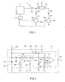
- FIGS. 1 and 2 identical or functionally identical elements are given the same reference numerals.
- FIG. 1 shows a schematic representation of an electronic ballast 1.
- the electronic ballast 1 is electrically connected to an electric lamp, which is formed in the embodiment shown as a fluorescent lamp 2.
- the electronic ballast 1 has a half-bridge inverter 11, which is electrically connected to an output with an inductance 12.
- the inductor 12 is further electrically connected to a first lamp filament 21 of the fluorescent lamp 2.
- the inductor 12 also has an electrical connection to a capacitor, which in the exemplary embodiment as a starting capacitor 13a is formed on.
- the ignition capacitor 13a may also be formed as an element of a voltage divider circuit for lamp voltage measurement, which may also be implemented as a resistor divider circuit.
- the electronic ballast 1 comprises a circuit arrangement 14a according to the invention for detecting a crest factor of a lamp burning voltage, which is electrically connected to a first input 141 to the first lamp filament 21 via the ignition capacitor 13a.
- a signal characterizing the lamp burning voltage is transmitted.
- a further capacitor which in the exemplary embodiment is designed as a half-bridge capacitor 13b, is connected to a second lamp filament 22.
- the half-bridge capacitor 13b has an electrical connection to ground potential. It should be noted that in the first embodiment, a circuit 14b is not present.
- the circuit arrangement 14a has a first output 142, which is electrically connected to a control unit 19.
- the circuit 14a is electrically connected to a second output at ground potential.
- the control unit 19 is also electrically connected to an output to an input of the half-bridge inverter 11.
- the circuit arrangement 14a according to the invention is thus designed to detect the crest factor of the lamp firing voltage.
- the second exemplary embodiment of the electronic ballast 1 according to the invention which is likewise shown in FIG. 1, will be explained in more detail below.
- the circuit arrangement 14a is not formed.
- the ignition capacitor 13a is guided to ground potential.
- the circuit arrangement 14b for detecting the crest factor of the lamp current is formed in the second exemplary embodiment.
- the circuit arrangement 14b is electrically connected with a first input 143 to the half-bridge capacitor 13b.
- the circuit arrangement 14b also has a first output 144 in the second exemplary embodiment, which is electrically connected to the control unit 19, wherein a second output of the circuit arrangement 14b is at ground potential.
- an electronic ballast 1 according to the invention either according to the first embodiment or realized according to the second embodiment.
- a realization in which both the signal paths from the inductance 12 via the ignition capacitor 13a via the circuit arrangement 14a to the control unit 19 and additionally the signal path from the second lamp coil 22 via the half-bridge capacitor 13b via the circuit arrangement 14b to the control unit 19 is realized is not provided ,
- FIG. 2 shows a detailed illustration of a circuit arrangement 14a or 14b according to the invention for detecting a crest factor of a lamp burning voltage or a lamp current.
- the circuit arrangement 14b for detecting the crest factor of the lamp current is considered in more detail below.
- the circuit arrangement 14b according to the invention has a first subcircuit 15, which is designed to determine an averaged value of the lamp current from an input signal applied to the circuit arrangement 14b via the input terminal 143.
- the first subcircuit 15 is formed in the embodiment as a low-pass circuit and has a resistor 151 and a capacitor 152.
- the resistor 151 is electrically connected at a first end to an input 15b of the first subcircuit 15 and at a second end to a circuit node of the first subcircuit 15.
- the capacitor 152 is also connected to the circuit node of the first subcircuit 15 and also has a second electrical connection to ground potential.
- the circuit arrangement 14b comprises a second subcircuit 16, which in the exemplary embodiment is designed to determine a maximum permissible value of the lamp current from the input signal applied to the circuit arrangement 14b.
- the second subcircuit 16 has an input 16b, which is electrically connected to the input terminal 143 of the circuit arrangement 14b.
- the second subcircuit 16 has a diode 161 and a capacitor 162.
- the diode 161 is connected with its anode to the input 16b of the second sub-circuit 16. With its cathode, the diode 161 is electrically connected to a first circuit node of the second sub-circuit 16.
- the second subcircuit 16 moreover has two resistors 163, 164 which are used for scaling the signal and for specifying a time constant for this signal, which is the maximum permissible value Crest factor characterized, is formed.
- the resistor 164 is connected to ground potential and connected to a second circuit node of the second subcircuit 16.
- the first resistor 163 is connected between the two circuit nodes of the second subcircuit 16.
- the first subcircuit 15 is connected to an output 15a to a first input 17a of a comparator circuit 17.
- An output 16a of the second subcircuit 16 is electrically connected to a second input 17b of this comparator circuit 17.
- the comparator circuit 17 is formed in the embodiment as a comparator.
- the circuit arrangement 14b in the illustrated embodiment comprises a third subcircuit 18, which is designed for processing and rectifying the input signal which is present at the input 143.
- the third subcircuit comprises a first diode 181 and a second diode 182.
- the first diode 181 is guided with its anode to ground potential, wherein it is connected with its cathode to a first circuit node of the third subcircuit.
- the second diode 182 is guided with its anode at the first circuit node and with its cathode to a second circuit node of the third subcircuit 18.
- the third subcircuit 18 also detects a resistor 183, which is electrically connected to the second circuit node and to ground potential.
- an output 18a of the third subcircuit 18 is electrically connected to the input 15b of the first subcircuit 15.
- the input signal applied to the input 143 is thus transmitted to the third sub-circuit 18 for conditioning and rectification.
- the rectified by this third sub-circuit 18 and processed input signal is then transmitted to the first sub-circuit 15, in which a signal is generated which characterizes the averaged value of the lamp current.
- the input signal applied to the input 143 is transmitted to the second subcircuit 16, in which a maximum permissible value is determined and in which an output signal is generated which characterizes the maximum permissible crest factor.
- the comparison signal generated by the comparator of the comparator circuit 17 is provided as an output signal of the circuit arrangement 14b at the output 144 and transmitted to the control unit 19.
- this control unit 19 is then a scheme with regard to a Setpoint of the crest factor of the lamp current is performed and transmit a corresponding signal to the half-bridge inverter 11.
- the subcircuits 15, 16 and 18 and / or the comparator circuit 17 are designed as digital circuits, thereby enabling digital detection of the processes respectively performed in the subcircuits.
- the sub-circuits 15, 16 and 18 and the comparator circuit 17 are implemented in a microprocessor and the entire detection of the crest factor, as carried out in the circuit 14b, takes place in a digital manner. This means that averaging, peak detection, scaling, timing, and threshold comparison are performed on a digital basis.
- the circuit arrangement 14a is analogous to the circuit arrangement 14b.
Applications Claiming Priority (1)
| Application Number | Priority Date | Filing Date | Title |
|---|---|---|---|
| DE102005027012A DE102005027012A1 (de) | 2005-06-10 | 2005-06-10 | Schaltungsanordnung und Verfahren zum Erfassen eines Crestfaktors eines Lampenstroms oder einer Lampenbrennspannung einer elektrischen Lampe |
Publications (2)
| Publication Number | Publication Date |
|---|---|
| EP1732365A2 true EP1732365A2 (fr) | 2006-12-13 |
| EP1732365A3 EP1732365A3 (fr) | 2007-10-24 |
Family
ID=36992021
Family Applications (1)
| Application Number | Title | Priority Date | Filing Date |
|---|---|---|---|
| EP06011752A Withdrawn EP1732365A3 (fr) | 2005-06-10 | 2006-06-07 | Circuit et méthode pour détecter le facteur de forme d' un courant à travers une lampe ou d' une tension aux bornes d' une lampe |
Country Status (5)
| Country | Link |
|---|---|
| US (1) | US7355356B2 (fr) |
| EP (1) | EP1732365A3 (fr) |
| CN (1) | CN1956617A (fr) |
| CA (1) | CA2549808A1 (fr) |
| DE (1) | DE102005027012A1 (fr) |
Cited By (1)
| Publication number | Priority date | Publication date | Assignee | Title |
|---|---|---|---|---|
| WO2008083855A1 (fr) | 2007-01-11 | 2008-07-17 | Osram Gesellschaft mit beschränkter Haftung | Procédé pour déterminer un facteur de crête d'un courant de lampe d'une lampe électrique |
Families Citing this family (2)
| Publication number | Priority date | Publication date | Assignee | Title |
|---|---|---|---|---|
| JP5380138B2 (ja) * | 2009-04-06 | 2014-01-08 | 本田技研工業株式会社 | 系統連系インバータ |
| DE102009023884A1 (de) * | 2009-06-04 | 2011-01-27 | Osram Gesellschaft mit beschränkter Haftung | Elektronisches Vorschaltgerät und Verfahren zum Betreiben mindestens einer Entladungslampe |
Citations (6)
| Publication number | Priority date | Publication date | Assignee | Title |
|---|---|---|---|---|
| US3502983A (en) * | 1968-11-20 | 1970-03-24 | Bell Telephone Labor Inc | Signal peak-to-average ratio detector |
| US5220276A (en) * | 1991-06-11 | 1993-06-15 | Keithley Corporation | Crest factor measurement device |
| US5363020A (en) * | 1993-02-05 | 1994-11-08 | Systems And Service International, Inc. | Electronic power controller |
| WO2000040058A1 (fr) * | 1998-12-29 | 2000-07-06 | Koninklijke Philips Electronics N.V. | Ballast electronique pour intensite variable comportant un seul etage de convertisseur a reaction |
| WO2002019779A1 (fr) * | 2000-08-28 | 2002-03-07 | Koninklijke Philips Electronics N.V. | Dispositif de circuit |
| WO2004028206A2 (fr) * | 2002-09-19 | 2004-04-01 | International Rectifier Corporation | Circuit de commande cfl adaptatif |
Family Cites Families (2)
| Publication number | Priority date | Publication date | Assignee | Title |
|---|---|---|---|---|
| EP1164819B1 (fr) * | 2000-06-15 | 2004-02-11 | City University of Hong Kong | Ballast réducteur eléctronique |
| JP4244747B2 (ja) * | 2002-11-08 | 2009-03-25 | ウシオ電機株式会社 | 高圧放電ランプ点灯装置 |
-
2005
- 2005-06-10 DE DE102005027012A patent/DE102005027012A1/de not_active Withdrawn
-
2006
- 2006-06-07 EP EP06011752A patent/EP1732365A3/fr not_active Withdrawn
- 2006-06-08 CA CA002549808A patent/CA2549808A1/fr not_active Abandoned
- 2006-06-09 CN CNA200610149512XA patent/CN1956617A/zh active Pending
- 2006-06-09 US US11/449,838 patent/US7355356B2/en active Active
Patent Citations (6)
| Publication number | Priority date | Publication date | Assignee | Title |
|---|---|---|---|---|
| US3502983A (en) * | 1968-11-20 | 1970-03-24 | Bell Telephone Labor Inc | Signal peak-to-average ratio detector |
| US5220276A (en) * | 1991-06-11 | 1993-06-15 | Keithley Corporation | Crest factor measurement device |
| US5363020A (en) * | 1993-02-05 | 1994-11-08 | Systems And Service International, Inc. | Electronic power controller |
| WO2000040058A1 (fr) * | 1998-12-29 | 2000-07-06 | Koninklijke Philips Electronics N.V. | Ballast electronique pour intensite variable comportant un seul etage de convertisseur a reaction |
| WO2002019779A1 (fr) * | 2000-08-28 | 2002-03-07 | Koninklijke Philips Electronics N.V. | Dispositif de circuit |
| WO2004028206A2 (fr) * | 2002-09-19 | 2004-04-01 | International Rectifier Corporation | Circuit de commande cfl adaptatif |
Cited By (1)
| Publication number | Priority date | Publication date | Assignee | Title |
|---|---|---|---|---|
| WO2008083855A1 (fr) | 2007-01-11 | 2008-07-17 | Osram Gesellschaft mit beschränkter Haftung | Procédé pour déterminer un facteur de crête d'un courant de lampe d'une lampe électrique |
Also Published As
| Publication number | Publication date |
|---|---|
| US7355356B2 (en) | 2008-04-08 |
| EP1732365A3 (fr) | 2007-10-24 |
| US20060279231A1 (en) | 2006-12-14 |
| DE102005027012A1 (de) | 2006-12-14 |
| CN1956617A (zh) | 2007-05-02 |
| CA2549808A1 (fr) | 2006-12-10 |
Similar Documents
| Publication | Publication Date | Title |
|---|---|---|
| EP0422255B1 (fr) | Ballast électronique | |
| EP0876742B1 (fr) | Procede et circuit de commande electronique pour la regulation des caracteristiques de fonctionnement de lampes a decharge | |
| DE60205830T2 (de) | Vorschaltgerät mit effizienter Elektroden-Vorheizung und Lampenfehlerschutz | |
| DE19900153A1 (de) | Integrierte Gate-Treiberschaltung | |
| EP2377372B1 (fr) | Méthode, appareil et système d'éclairage | |
| DE69911376T2 (de) | Verfahren und anordnung zum betreiben von elektronischen vorschaltgeräten für entladungslampen hoher intensität | |
| DE102004039421B4 (de) | Vorschaltgerät einer Entladungslampe und Verfahren zum Ansteuern einer Entladungsleuchte | |
| EP2258149B1 (fr) | Détection du type d'une lampe hid par un ballast pour lampes multiples et système d'éclairage | |
| EP1901591B1 (fr) | Allumage de lampes à décharge dans des conditions environnementales variables | |
| EP1732365A2 (fr) | Circuit et méthode pour détecter le facteur de forme d' un courant à travers une lampe ou d' une tension aux bornes d' une lampe | |
| EP1424881B1 (fr) | Dispositif et méthode pour commander une lampe fluorescente | |
| EP1276355B1 (fr) | Circuit ballast pour determiner la puissance de préchauffage | |
| DE60122192T2 (de) | Schaltungsanordnung | |
| EP2274960B1 (fr) | Procédé et agencement de circuits pour faire fonctionner au moins une lampe à décharge | |
| EP1992203B1 (fr) | Ballasst électronique et procédé de fonctionnement d'une lampe électrique | |
| WO2008128577A1 (fr) | Circuiterie pour l'allumage et l'utilisation d'une lampe à décharge | |
| EP2208401B1 (fr) | Ballast électronique et procédé pour faire fonctionner au moins une première et une deuxième lampes à décharge | |
| DE102020103921B4 (de) | Betriebsvorrichtung und Verfahren zum Betreiben einer Leuchtmittelanordnung | |
| DE102004037389A1 (de) | Verfahren zur Ansteuerung einer eine Leuchtstofflampe aufweisenden Last zur Optimierung des Zündvorganges | |
| EP3580824B1 (fr) | Circuit de limitation du courant d'appel pour un bloc d'alimentation | |
| EP3195698B1 (fr) | Ballast électronique et procédé de commande d'une charge | |
| DE10127135B4 (de) | Dimmbares elektronisches Vorschaltgerät | |
| DE102005018763A1 (de) | Betriebsgeräte mit Auswertung der Lampentemperatur bei der Lampenregelung | |
| WO2008083855A1 (fr) | Procédé pour déterminer un facteur de crête d'un courant de lampe d'une lampe électrique | |
| DE102009053617A1 (de) | Elektronisches Vorschaltgerät und Verfahren zum Betreiben mindestens einer Entladungslampe |
Legal Events
| Date | Code | Title | Description |
|---|---|---|---|
| PUAI | Public reference made under article 153(3) epc to a published international application that has entered the european phase |
Free format text: ORIGINAL CODE: 0009012 |
|
| AK | Designated contracting states |
Kind code of ref document: A2 Designated state(s): AT BE BG CH CY CZ DE DK EE ES FI FR GB GR HU IE IS IT LI LT LU LV MC NL PL PT RO SE SI SK TR |
|
| AX | Request for extension of the european patent |
Extension state: AL BA HR MK YU |
|
| PUAL | Search report despatched |
Free format text: ORIGINAL CODE: 0009013 |
|
| AK | Designated contracting states |
Kind code of ref document: A3 Designated state(s): AT BE BG CH CY CZ DE DK EE ES FI FR GB GR HU IE IS IT LI LT LU LV MC NL PL PT RO SE SI SK TR |
|
| AX | Request for extension of the european patent |
Extension state: AL BA HR MK YU |
|
| AKX | Designation fees paid | ||
| STAA | Information on the status of an ep patent application or granted ep patent |
Free format text: STATUS: THE APPLICATION IS DEEMED TO BE WITHDRAWN |
|
| 18D | Application deemed to be withdrawn |
Effective date: 20080425 |
|
| REG | Reference to a national code |
Ref country code: DE Ref legal event code: 8566 |